US5796276A - High-side-driver gate drive circuit - Google Patents
High-side-driver gate drive circuit Download PDFInfo
- Publication number
- US5796276A US5796276A US08/366,781 US36678194A US5796276A US 5796276 A US5796276 A US 5796276A US 36678194 A US36678194 A US 36678194A US 5796276 A US5796276 A US 5796276A
- Authority
- US
- United States
- Prior art keywords
- current
- circuit
- gate
- error amplifier
- source
- Prior art date
- Legal status (The legal status is an assumption and is not a legal conclusion. Google has not performed a legal analysis and makes no representation as to the accuracy of the status listed.)
- Expired - Lifetime
Links
Images


Classifications
-
- H—ELECTRICITY
- H03—ELECTRONIC CIRCUITRY
- H03K—PULSE TECHNIQUE
- H03K17/00—Electronic switching or gating, i.e. not by contact-making and –breaking
- H03K17/06—Modifications for ensuring a fully conducting state
- H03K17/063—Modifications for ensuring a fully conducting state in field-effect transistor switches
Definitions
- the present invention relates to integrated circuits for driving half-bridge and/or H-bridge circuits, and particularly to power integrated circuits which include power transistors on-chip.
- One of the most basic power circuit configurations is a bridge circuit, in which pull-up and pull-down transistors selectably pull a load node in opposite directions.
- a related common structure is the H-bridge circuit, in which each of two connections to a load is connected to a half-bridge circuit. (This is particularly useful for motor control, since current can be driven through the load in either of two opposite directions.)
- N-channel power FETs e.g. VDMOS devices
- Vs will be a "raw" external power supply voltage, which provides the high-current drive for the power transistors.
- Vdd will be a reduced and filtered voltage (e.g. 5 V) which powers the logic elements.
- Vcp will be a boosted voltage, typically 15 Volts higher than the system supply Vs, i.e. about 28 V above ground in a vehicular system. However, in some cases Vcp may be as low as Vs+7 V or as high as Vs+22 V.
- This boosted voltage is used to give the FETs a large gate overdrive voltage in their on-state, and thereby permits the on-state resistance of the FETs to be reduced. Moreover, when such a boosted voltage is used, the pull-up and pull-down transistors can both be NMOS, without any need for power PMOS or PNP devices.
- the gate voltage is normally supplied by a current source from Vcp (to prevent an excessively sharp turn-on transient, with resulting glitch problems).
- the overdrive voltage Vcp is normally generated on-chip by a charge pump. However, this can cause a problem: suppose that one of the low side drivers on one leg is shorted to ground. The source of the high side driver on that side will therefore be pulled down; and therefore, because of the gate protection circuit, the gate of the high side driver will follow; and therefore the boosted-voltage supply line, which supplies the gate voltages, can be overloaded and pulled down well below its specified range.
- Some chips include a protection circuit which monitors the charge pump voltage and disables the chip under low Vcp conditions. Without such a protection, some of the transistors may be shifted into their analog range of operation, which may increase their heat dissipation to the point where they are destroyed.
- the conventional solution to this problem is simply to provide multiple separate charge pumps (one for each transistor). This requires increased area for the diode-capacitor chains (and particularly for the isolation between them).
- the present application provides a different innovative solution, which avoids the need for paralleled charge pumps.
- a current-mode differential error amplifier is used to regulate the current sourced to the gate.
- a current path is provided from the gate to the source of the power device, and a constant current is provided to the gate.
- a variable current source is also provided, and this current source is controlled by the output of the error amplifier.
- a voltage offset (avalanche breakdown diode) is interposed between the gate and source of the high-side driver; this ensures that the feedback loop will operate in a bistable mode, which avoids instability problems.
- the maximum current is chosen, for a given target power device, to give the desired slew rate for charging the gate.
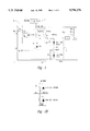
- FIG. 1 is a very high-level schematic drawing which conceptually shows some principles of the invention.
- FIGS. 2a-2b is a simplified schematic view of an innovative high-side gate drive circuit as provided by the present invention.
- FIG. 3A is a block diagram view of a complete smart-power integrated circuit which uses the circuit of FIG. 2, and FIG. 3B is a more detailed schematic of this integrated circuit.
- FIG. 4 is a more detailed schematic of the block H-BRIDGE in FIG. 3B.
- FIG. 5 shows a further detail of the GATE -- DRIVE block in FIG. 4, showing how the driver logic controls both a DRIVER -- HI circuit and a DRIVER -- LO circuit.
- FIG. 1 is a conceptual diagram which shows important principles of the invention.
- a circuit 9 represents a driver circuit, several of which can be coupled to one pumped voltage circuit.
- Voltage VCP is a pumped voltage 32, derived from pumping the battery voltage through charge pump 7, e.g. about 15 V above battery voltage in this example.
- a current source I OFFSET , I 18 provides a constant current from Vcp to the gate 20 of the high side driver transistor. (In the presently preferred embodiment, I OFFSET is twice as much as I REF .) This current will maintain diode Z at its breakdown voltage (about 10 V in this example) after the power transistor gate has been fully charged up.
- Diode Z sinks current from the high side driver's gate to the output terminal 22. This current is monitored, and provides one input I 14 to the current-controlled differential error amplifier EA. The other input is provided by a current mirror I 12 of the reference current I REF , I 10 , (as long as switch ON/OFF 26 has not been activated to remove this current input from the error amplifier). The error amplifier accordingly provides a current I VARIABLE , I 16 (also sourced from V CP ) to the gate terminal.
- the basic control loop attempts to regulate I VARIABLE so that the negative current input to the error amplifier is equal to I REF .
- the control loop When the control loop is first turned on, no gate-source current will flow, and the error amplifier will therefore turn on I VARIABLE to charge the gate rapidly (with about 500 ⁇ A, in the presently preferred embodiment). If the source of the high side driver is pulled down, the current through the diode Z will become large, and the current supplied to the negative input of the error amplifier will therefore be larger than I REF . I VARIABLE will therefore be off, and the boosted supply line V CP will be loaded only by I OFFSET and not by I VARIABLE .
- FIG. 2A shows a sample implementation (which is currently preferred) of the innovative circuit 5, represented in FIG. 1.
- Input VBG is a precision voltage from a bandgap reference, and provides a constant current through bipolar Q0 (about 20 microamps, in the presently preferred embodiment). This current is mirrored over to PMOS current source M104. The current from M104 ( ⁇ 10 ⁇ A) is divided between transistor M9 and Q1. Q1 is on the receiving end of a current mirror, so M9 receives a current which is defined by a differencing relationship. The importance of this relationship will now be discussed in greater detail.
- Transistor M9 is a diode connected VDMOS to ground, and serves as the input to current mirror M9/M8.
- M8 drives the mirrored current onto PMOS M107, which is a diode-connected P-channel which is then mirrored onto M108.
- M108 is a very large P-channel (40 times the size of M107), which supplies approximately half a milliamp during the charging phase of the output device. That current provides the supply current for the Q101/Q102 mirror.
- the current differencing amplifier is hard-on. It is slewed to one end of its operation, with the drain of M104 up at nearly 5 volts, and all the current from M104 going into M9 and being mirrored up to supply the maximum current to the gate to pass through the output device. In this state, Q102 is totally off.
- M109 supplies 20 microamps, and when this target condition is reached, M109 causes the current differencing amplifier to slew from the hard-on mode of operation over the opposite (hard-off) mode of operation, and the collector of Q1 will fall to zero (i.e. Q1 will saturate).
- Vcp the load on Vcp is limited to 20 microamps, which means that the other gate control circuits are not disrupted.
- the transient current used to charge the gate capacitance of the high side driver at turn-on is about half milliamp (500 ⁇ A), and the trickle current from the charge pump into the circuit is about 40 microamps (current drawn by the current mirror and the two zeners).
- the charge pump can supply about 200 microamps. In a single H-bridge, two transistors will be on at the same time; but the output capacitor of the charge pump lets it supply increased current transiently.
- the transistor gate is charged up, at turn-on, in about four microseconds; but of course this can be readily changed by changing the charge pump's storage capacitor size, or by changing the power transistor's dimensions.
- FIG. 2A also shows other circuitry which is used in the presently preferred embodiment.
- Q100 is a large PNP (18 times the minimum area), which is used for shorting out the gate to source of the output device at turn-off. (At turn-off the regulated current input to mirror M4/M5 is bypassed by M0.)
- the body diodes of the VDMOS power devices pass the inductive current. Switches M0, M1, and M2 just turn on current sources to turn it from one mode to the other, i.e. from on to off or vice versa.
- FIG. 2B shows the gate driving output 20 and circuit output 22 of FIG. 2A coupled to a driver transistor system.
- the high side driver is connected between the battery voltage and the output 22, while the low side driver is connected between the output and ground 24.
- the circuit for driving the low side driver power device is not shown, and is known in the art.
- FIG. 3A is a block diagram view of a complete smart-power integrated circuit which uses the circuit of FIG. 2.
- This sample embodiment is a stepper motor driver circuit, which incorporates all the necessary power and logic functions to drive a two phase bipolar stepper motor in half-step or full-step mode with an output current in excess of 0.75 A.
- Notable features of this chip include the provision of: two h-bridge drivers; internal waveform generation; short-circuit (shorted load) and thermal protection; and open-circuit (open load) detection.
- the pin function/assignments are as follows:
- FIG. 3B is a more detailed schematic of the integrated circuit of FIG. 3A. Note that two H-bridge circuits H-BRIDGE are shown. These are controlled by block CONTROL -- LOGIC, which also provides a fault-detection signal FAULT off-chip.
- Block CHARGE -- PUMP provides the pumped voltage V CP
- block UVOV which is connected to receive the battery voltage V S , pumped voltage V CP , and power ground PGND detects undervoltage and overvoltage conditions.
- Block INPUT -- BUFFER provides a serial interface.
- the OVER -- TEMPERATURE, BANDGAP, and DELAY25 blocks provide the overtemperature detection, a bandgap voltage reference, and a delay line respectively.
- FIG. 4 is a more detailed schematic of the block H-BRIDGE in FIG. 3B.
- the basic bridge circuit includes large n-channel VDMOS drivers MHA, MHB, MLA, and MLA, connected to form two half-bridge circuits MHA/MLA (driving terminal OUTA) and MHB/MLB (driving terminal OUTB).
- the logic at lower right detects open and short conditions.
- FIG. 5 shows further detail of the GATE -- DRIVE block in FIG. 4, showing how the driver logic DRIVER -- LOGIC controls both a DRIVER -- HI circuit and a DRIVER -- LO circuit.
- FIG. 2 is a detailed view of the DRIVER -- HI circuit.
- a method for driving a gate drive output connection for controlling a voltage-controlled semiconductor power switching device, comprising the steps of: (a.) operating a differential current-mode error amplifier which compares the current passed externally from a gate terminal to a first source/drain terminal of the switching device with a reference current; and (b.) providing a variable current to the gate of the power switching device, through a current source which is controlled by the output of said error amplifier; (c.) wherein said error amplifier is connected to increase said variable current when said current passed externally from gate to said first source/drain terminal of the switching device becomes less than said reference current; whereby when said error amplifier and reference current are turned on while said gate is discharged, said error amplifier increases said variable current to a maximum value.
- a method for driving a gate drive output connection for controlling a voltage-controlled semiconductor power switching device, comprising the steps of: (a.) operating a differential current-mode error amplifier which compares the current passed externally from a gate terminal to a first source/drain terminal of the switching device with a reference current; and (b.) providing a variable current to the gate of the power switching device, through a current source which is controlled by the output of said error amplifier; (c.) wherein said error amplifier is connected to increase said variable current when said current passed externally from gate to said first source/drain terminal of the switching device becomes less than said reference current; (d.) providing a constant offset current to the gate of the power switching device, and providing a voltage offset between the gate and source of the power switching device; whereby when said error amplifier and reference current are turned on while said gate is discharged, said error amplifier increases said variable current to a maximum value.
- a method for driving a gate drive output connection for controlling a voltage-controlled semiconductor power switching device, comprising the steps of: (a.) providing a reference current; (b.) diverting a portion of said reference current into at least a first circuit branch, said first circuit branch drawing an amount of current which is dependent on the voltage of the gate drive output; (c.) connecting the remaining portion of said reference current to drive a second circuit branch which is operatively connected to provide current to the gate drive output in dependence on the remaining portion of said reference current.
- a method for driving a gate drive output connection for controlling a voltage-controlled semiconductor power switching device, comprising the steps of: (a.) providing a reference current; (b.) diverting a portion of said reference current into at least a first circuit branch, said first circuit branch drawing an amount of current which is dependent on the voltage of the gate drive output, and which is zero unless the gate drive output exceeds a predetermined minimum voltage; (c.) connecting the remaining portion of said reference current to drive a second circuit branch which is operatively connected to provide current to the gate drive output in dependence on the remaining portion of said reference current.
- a method for driving a gate drive output connection for controlling a voltage-controlled semiconductor power switching device, comprising the steps of: (a.) providing a reference current; (b.) diverting a portion of said reference current into at least a first circuit branch, said first circuit branch drawing an amount of current which is dependent on the voltage of the gate drive output; (c.) connecting the remaining portion of said reference current to drive a second circuit branch which is operatively connected, through feedback circuitry, to provide current to the gate drive output in dependence on the remaining portion of said reference current, wherein said feedback circuitry imposes a divergence relation to reach one of only two stable steady-state conditions.
- a method for controlling a plurality of bridge circuits which each include pull-up and pull-down power transistors operatively connected in series comprising the steps of: I.) generating a pumped voltage, in a single charge-pumping circuit, which is more extreme than any power supply voltage; and II.) operating each of a plurality of gate drive circuits, all powered by said pumped voltage from said single charge-pumping circuit, with the steps of (a.) providing a reference current; (b.) diverting a portion of said reference current into at least a first circuit branch, said first circuit branch drawing an amount of current which is dependent on the voltage of the gate drive output; and (c.) connecting the remaining portion of said reference current to drive a second circuit branch which is operatively connected to provide current to the gate drive output in dependence on the remaining portion of said reference current; whereby if any one of said gate drive circuits is driving a high-side driver transistor whose source is shorted to ground, the charge-p
- an integrated circuit for controlling a plurality of power transistors comprising: a plurality of gate driving circuits, each connected to provide a gate voltage to at least one respective one of said respective power transistors; wherein at least one of said gate driving circuits comprises a differential error amplifier which is connected to receive, as differential inputs, a reference current, and a current corresponding to the current passed externally from a gate terminal to a first source/drain terminal of the switching device; a variable current source, connected to provide current to the gate of the power switching device, in dependence on the output of said error amplifier; a constant current source, connected to provide a constant current to the gate of the respective power transistor; and a voltage source interposed between gate and source of the respective power transistor; wherein said error amplifier is connected to increase said variable current when said reference current becomes greater than the other input to said error amplifier.
- An integrated H-bridge driver circuit comprising: a plurality of gate driving circuits, each connected to provide a gate voltage to at least one respective one of said respective power transistors; wherein at least one of said gate driving circuits comprises first and second bridge circuits, each including a pull-up transistor and a pull-down transistor with an output node therebetween, said output nodes of said first and second bridge circuits providing first and second respective load connections; a differential error amplifier which is connected to receive, as differential inputs, a reference current, and a current corresponding to the current passed externally from a gate terminal to a first source/drain terminal of the switching device; and a variable current source, connected to provide current to the gate of the power switching device, in dependence on the output of said error amplifier; wherein said error amplifier is connected to increase said variable current when said reference current becomes greater than the other input to said error amplifier.
- An integrated bridge circuit comprising a voltage augmenting circuit connected to receive a first supply voltage and generate an augmented voltage which not in the range of said first and second supply voltages, inclusive; high-side and low-side power field-effect transistors connected in series between said first and second supply voltages, and an output connection intermediate between said transistors; wherein said power transistors are both operatively connected to receive a gate voltage from respective gate driving circuits which are both driven by said augmented voltage; and wherein at least one said gate driving circuit includes a differential error amplifier which is connected to receive, as differential inputs, a reference current, and a current corresponding to the current passed externally from a gate terminal to a first source/drain terminal of the switching device; and a variable current source, connected to provide current to the gate of the power switching device, in dependence on the output of said error amplifier; wherein said error amplifier is connected to increase said variable current when said reference current becomes greater than the other input to said error amplifier.
- FIGS. 2-5) can be modified in a tremendous variety of ways.
- some circuit elements can be repositioned, or additional stages can be inserted.
- FET devices can be replaced by bipolars or vice versa. (Bipolars, however, do tend to provide greater headroom in current mirrors.)
- the power transistors being controlled can optionally be discrete rather than integrated.
- the power field-effect transistors being controlled can optionally be replaced by other analogous device structures, such as IGBTs, voltage-controlled thyristors, etc.
- the invention is particularly applicable to devices having a current-supplied capacitive gate.
- the disclosed circuit can be used with more or fewer bridge circuits; in particular, the advantages of the invention are increase when more bridge circuits or independent switching circuits are present on the chip.
- the invention is expected to be even more applications for three-phase motor drivers, where three H-bridge switches are used to drive three windings.
- the basic idea of the innovative current differencing amplifier can be done in many ways.
- the configuration and connections of the differential error amplifier could be shifted in a wide variety of ways, and/or the offset contribution could be added using other circuit elements.
Abstract
A high-side gate driving circuit, where a current-mode differential error amplifier is used to regulate the current sourced to the gate. A current path is provided from the gate to the source of the power device, and a constant current is provided to the gate. A variable current source is also provided, and this current source is controlled by the output of the error amplifier. Preferably a voltage offset (avalanche breakdown diode) is interposed between the gate and source of the high-side driver; this ensures that the feedback loop will operate in a bistable mode, which avoids instability problems.
Description
The present invention relates to integrated circuits for driving half-bridge and/or H-bridge circuits, and particularly to power integrated circuits which include power transistors on-chip.
One of the most basic power circuit configurations is a bridge circuit, in which pull-up and pull-down transistors selectably pull a load node in opposite directions. A related common structure is the H-bridge circuit, in which each of two connections to a load is connected to a half-bridge circuit. (This is particularly useful for motor control, since current can be driven through the load in either of two opposite directions.) In power integrated circuits, such drivers are commonly implemented with N-channel power FETs (e.g. VDMOS devices).
In smart power chips there will often be several relevant power supply voltages (in addition to ground). Vs will be a "raw" external power supply voltage, which provides the high-current drive for the power transistors. (For example, in automotive systems this will typically be 13 V nominal, with a large variation due to poor regulation.) Vdd will be a reduced and filtered voltage (e.g. 5 V) which powers the logic elements. Vcp will be a boosted voltage, typically 15 Volts higher than the system supply Vs, i.e. about 28 V above ground in a vehicular system. However, in some cases Vcp may be as low as Vs+7 V or as high as Vs+22 V. (This boosted voltage is used to give the FETs a large gate overdrive voltage in their on-state, and thereby permits the on-state resistance of the FETs to be reduced. Moreover, when such a boosted voltage is used, the pull-up and pull-down transistors can both be NMOS, without any need for power PMOS or PNP devices.)
When one of the transistors is turned on, the gate voltage is normally supplied by a current source from Vcp (to prevent an excessively sharp turn-on transient, with resulting glitch problems).
The overdrive voltage Vcp is normally generated on-chip by a charge pump. However, this can cause a problem: suppose that one of the low side drivers on one leg is shorted to ground. The source of the high side driver on that side will therefore be pulled down; and therefore, because of the gate protection circuit, the gate of the high side driver will follow; and therefore the boosted-voltage supply line, which supplies the gate voltages, can be overloaded and pulled down well below its specified range.
If the boosted-voltage supply line is shared among multiple gate drive circuits, this can cause problems. Some chips (as in the presently preferred embodiment) include a protection circuit which monitors the charge pump voltage and disables the chip under low Vcp conditions. Without such a protection, some of the transistors may be shifted into their analog range of operation, which may increase their heat dissipation to the point where they are destroyed.
The conventional solution to this problem is simply to provide multiple separate charge pumps (one for each transistor). This requires increased area for the diode-capacitor chains (and particularly for the isolation between them). However, the present application provides a different innovative solution, which avoids the need for paralleled charge pumps.
In the present invention, a current-mode differential error amplifier is used to regulate the current sourced to the gate. A current path is provided from the gate to the source of the power device, and a constant current is provided to the gate. A variable current source is also provided, and this current source is controlled by the output of the error amplifier. Preferably a voltage offset (avalanche breakdown diode) is interposed between the gate and source of the high-side driver; this ensures that the feedback loop will operate in a bistable mode, which avoids instability problems. The maximum current is chosen, for a given target power device, to give the desired slew rate for charging the gate.
The disclosed inventions will be described with reference to the accompanying drawings, which show important sample embodiments of the invention and which are incorporated in the specification hereof by reference, wherein:
FIG. 1 is a very high-level schematic drawing which conceptually shows some principles of the invention.
FIGS. 2a-2b is a simplified schematic view of an innovative high-side gate drive circuit as provided by the present invention.
FIG. 3A is a block diagram view of a complete smart-power integrated circuit which uses the circuit of FIG. 2, and FIG. 3B is a more detailed schematic of this integrated circuit.
FIG. 4 is a more detailed schematic of the block H-BRIDGE in FIG. 3B.
FIG. 5 shows a further detail of the GATE-- DRIVE block in FIG. 4, showing how the driver logic controls both a DRIVER-- HI circuit and a DRIVER-- LO circuit.
The numerous innovative teachings of the present application will be described with particular reference to the presently preferred embodiment (by way of example, and not of limitation), in which:
FIG. 1 is a conceptual diagram which shows important principles of the invention. A circuit 9 represents a driver circuit, several of which can be coupled to one pumped voltage circuit. Voltage VCP is a pumped voltage 32, derived from pumping the battery voltage through charge pump 7, e.g. about 15 V above battery voltage in this example. A current source IOFFSET, I18, provides a constant current from Vcp to the gate 20 of the high side driver transistor. (In the presently preferred embodiment, IOFFSET is twice as much as IREF.) This current will maintain diode Z at its breakdown voltage (about 10 V in this example) after the power transistor gate has been fully charged up.
Diode Z sinks current from the high side driver's gate to the output terminal 22. This current is monitored, and provides one input I14 to the current-controlled differential error amplifier EA. The other input is provided by a current mirror I12 of the reference current IREF, I10, (as long as switch ON/OFF 26 has not been activated to remove this current input from the error amplifier). The error amplifier accordingly provides a current IVARIABLE, I16 (also sourced from VCP) to the gate terminal.
Thus, the basic control loop attempts to regulate IVARIABLE so that the negative current input to the error amplifier is equal to IREF. When the control loop is first turned on, no gate-source current will flow, and the error amplifier will therefore turn on IVARIABLE to charge the gate rapidly (with about 500 μA, in the presently preferred embodiment). If the source of the high side driver is pulled down, the current through the diode Z will become large, and the current supplied to the negative input of the error amplifier will therefore be larger than IREF. IVARIABLE will therefore be off, and the boosted supply line VCP will be loaded only by IOFFSET and not by IVARIABLE.
FIG. 2A shows a sample implementation (which is currently preferred) of the innovative circuit 5, represented in FIG. 1.
Input VBG is a precision voltage from a bandgap reference, and provides a constant current through bipolar Q0 (about 20 microamps, in the presently preferred embodiment). This current is mirrored over to PMOS current source M104. The current from M104 (≠10 μA) is divided between transistor M9 and Q1. Q1 is on the receiving end of a current mirror, so M9 receives a current which is defined by a differencing relationship. The importance of this relationship will now be discussed in greater detail.
If the loop had no external constraints on it, it would try to regulate the loop such that M104 drain and Q2 collector current were almost the same (M9 carrying 1/20 of the current on the zeners, i.e. divided by the gain of the feedback path). Note that the output of PNP current mirror Q101/Q102 is mirrored (and doubled) to drive Q1; so consider what drives the input side (Q102) of the Q11/Q102 mirror: Q102 is connected, through zener (or avalanche) diodes D1 and D2, to the source (low) side of the high-side driver transistor. These two zener diodes have about 5.5 volts breakdown each, which (with a Vbe drop) defines a limit of about 12 volts maximum gate-source voltage on the output device.
Transistor M9 is a diode connected VDMOS to ground, and serves as the input to current mirror M9/M8. M8 drives the mirrored current onto PMOS M107, which is a diode-connected P-channel which is then mirrored onto M108. M108 is a very large P-channel (40 times the size of M107), which supplies approximately half a milliamp during the charging phase of the output device. That current provides the supply current for the Q101/Q102 mirror.
Thus Q102 only turns on (and the error amplifier loop only turns on) once the gate-source voltage of the power device has risen to something like 12 Volts.
One potential problem with this current differencing amplifier is that you have stability issues because it is a control loop, and there's no high impedance node to hang a stabilizing capacitor from. (However, it is preferable not to use such a capacitor anyway, because of the area consumption.) The present invention avoids this problem, since the current differencing amplifier loop only operates in two states: it is either hard-on or hard-off.
During charging of the power device, the current differencing amplifier is hard-on. It is slewed to one end of its operation, with the drain of M104 up at nearly 5 volts, and all the current from M104 going into M9 and being mirrored up to supply the maximum current to the gate to pass through the output device. In this state, Q102 is totally off.
Now suppose that the error amplifier gets to the point where it would like to regulate (i.e. M104 passing 10 microamps, the Q1 collector passing 10 microamps, Q2's collector passing 5 microamps, Q101 and Q102 passing 5 microamps each, so that a total current of 10 microamps is being supplied from Vcp by M108). M109 supplies 20 microamps, and when this target condition is reached, M109 causes the current differencing amplifier to slew from the hard-on mode of operation over the opposite (hard-off) mode of operation, and the collector of Q1 will fall to zero (i.e. Q1 will saturate).
Thus the effect of the offset contribution, caused by M109 constantly supplying 20 microamps into the gate of the output device, is to prevent the current differencing amplifier from ever staying in its analog range. Hence no stability issues appear (except transiently during turn on, and oscillation during this transient period is not really important). If the gate-source capacitance of the output device ever becomes discharged for some reason, the current differencing amplifier will immediately act to charge it back up again.
Now, consider the implication of this for the operating condition discussed in the Background section above. When the source of the high side driver is shorted to ground, the gate of the output device is pulled to 12 volts above ground 24 (by the opposed transistor Q102 and diodes D1 and D2). But with the innovative circuit of FIG. 2, because the current differencing amplifier is still slewed in its "off" state, the only current to be supplied to the circuit via M109 will be 20 microamps.
Thus, even under worst conditions, the load on Vcp is limited to 20 microamps, which means that the other gate control circuits are not disrupted.
In the presently preferred embodiment, the transient current used to charge the gate capacitance of the high side driver at turn-on is about half milliamp (500 μA), and the trickle current from the charge pump into the circuit is about 40 microamps (current drawn by the current mirror and the two zeners). The charge pump can supply about 200 microamps. In a single H-bridge, two transistors will be on at the same time; but the output capacitor of the charge pump lets it supply increased current transiently.
In the presently preferred embodiment, the transistor gate is charged up, at turn-on, in about four microseconds; but of course this can be readily changed by changing the charge pump's storage capacitor size, or by changing the power transistor's dimensions.
FIG. 2A also shows other circuitry which is used in the presently preferred embodiment. Q100 is a large PNP (18 times the minimum area), which is used for shorting out the gate to source of the output device at turn-off. (At turn-off the regulated current input to mirror M4/M5 is bypassed by M0.) The body diodes of the VDMOS power devices pass the inductive current. Switches M0, M1, and M2 just turn on current sources to turn it from one mode to the other, i.e. from on to off or vice versa.
FIG. 2B shows the gate driving output 20 and circuit output 22 of FIG. 2A coupled to a driver transistor system. The high side driver is connected between the battery voltage and the output 22, while the low side driver is connected between the output and ground 24. The circuit for driving the low side driver power device is not shown, and is known in the art.
FIG. 3A is a block diagram view of a complete smart-power integrated circuit which uses the circuit of FIG. 2. This sample embodiment is a stepper motor driver circuit, which incorporates all the necessary power and logic functions to drive a two phase bipolar stepper motor in half-step or full-step mode with an output current in excess of 0.75 A. Notable features of this chip include the provision of: two h-bridge drivers; internal waveform generation; short-circuit (shorted load) and thermal protection; and open-circuit (open load) detection.
The pin function/assignments, in this sample embodiment, are as follows:
______________________________________ PIN NAME FUNCTION ______________________________________ 1 PGND Power Ground (Return For VS1) 2 OUT1A Motor Drive H-Bridge 1, Output A 3 VS1 Switched Battery Power Supply Input 1 4 OUT1B Motor Drive H-Bridge 1,Output B 5 VCP Charge Pump Capacitor 6 VDD 5v Logic Power Supply Input 7 OUT2B Motor Drive H-Bridge 2, Output A 8 VS2 Switched Battery Power Supply Input 2 9 OUT2A Motor Drive H-Bridge 2, Output B 10 PGND Power Ground (Return For VS2) 11 PGND Power Ground (Return For VS2) 12 SGND Signal Ground (Return For VDD) 13 FAULT Over-current/Open-load/Over-temperature Fault Indicator Logic Output (Active High) 14 SMODE Step Mode Logic Input - Full or Half Step (Logic High = Full-step, Logic Low = Half-step) 15 SCLK Motor Control Logic Clock Input (Internal Logic Clocked on Rising Edge) 16 EN2 H-Bridge 2 Enable Logic Input (Active High) 17 EN1 H-Bridge 1 Enable Logic Input (Active High) 18 DIR Motor Direction Logic Input 19 RESET Reset Logic input (Active Low) 20 PGND Power Ground (Return For VS1) ______________________________________
The absolute maximum ratings of this device, in this sample embodiment, are as follows:
______________________________________
Symbol Parameter        Value         Unit
______________________________________
Vs     Switched Battery Supply
                        -0.3 . . . 45 VDC
       Voltage
Vs     Switched Battery Supply
                        -1.5          V
       Voltage Negative
       Transient
       (100 mS + 100Ω
       Source Impedance)
Vdd    Logic Power Supply
                        -0.3 . . . 7.0
                                      VDC
Vin    Logic Input Voltage
                        -0.3 . . . Vdd + 0.5
                                      VDC
Tj     Junction Temperature
                        -40 . . . 150 °C.
Tst    Storage Temperature
                        -65 . . . 150 °C.
Pd     Power Dissipation
                        Limited Internally
                                      W
Iout   Maximum Output Current
                        0.75          A
Continuous
       Limited Inter-   A
Non-Repetitive
       nally
______________________________________
FIG. 3B is a more detailed schematic of the integrated circuit of FIG. 3A. Note that two H-bridge circuits H-BRIDGE are shown. These are controlled by block CONTROL-- LOGIC, which also provides a fault-detection signal FAULT off-chip. Block CHARGE-- PUMP provides the pumped voltage VCP, and block UVOV, which is connected to receive the battery voltage VS, pumped voltage VCP, and power ground PGND detects undervoltage and overvoltage conditions. Block INPUT-- BUFFER provides a serial interface. The OVER-- TEMPERATURE, BANDGAP, and DELAY25 blocks provide the overtemperature detection, a bandgap voltage reference, and a delay line respectively.
FIG. 4 is a more detailed schematic of the block H-BRIDGE in FIG. 3B. The basic bridge circuit includes large n-channel VDMOS drivers MHA, MHB, MLA, and MLA, connected to form two half-bridge circuits MHA/MLA (driving terminal OUTA) and MHB/MLB (driving terminal OUTB). The logic at lower right detects open and short conditions.
FIG. 5 shows further detail of the GATE-- DRIVE block in FIG. 4, showing how the driver logic DRIVER-- LOGIC controls both a DRIVER-- HI circuit and a DRIVER-- LO circuit. (FIG. 2 is a detailed view of the DRIVER-- HI circuit.)
According to a disclosed class of innovative embodiments, there is provided: A method for driving a gate drive output connection, for controlling a voltage-controlled semiconductor power switching device, comprising the steps of: (a.) operating a differential current-mode error amplifier which compares the current passed externally from a gate terminal to a first source/drain terminal of the switching device with a reference current; and (b.) providing a variable current to the gate of the power switching device, through a current source which is controlled by the output of said error amplifier; (c.) wherein said error amplifier is connected to increase said variable current when said current passed externally from gate to said first source/drain terminal of the switching device becomes less than said reference current; whereby when said error amplifier and reference current are turned on while said gate is discharged, said error amplifier increases said variable current to a maximum value.
According to another disclosed class of innovative embodiments, there is provided: A method for driving a gate drive output connection, for controlling a voltage-controlled semiconductor power switching device, comprising the steps of: (a.) operating a differential current-mode error amplifier which compares the current passed externally from a gate terminal to a first source/drain terminal of the switching device with a reference current; and (b.) providing a variable current to the gate of the power switching device, through a current source which is controlled by the output of said error amplifier; (c.) wherein said error amplifier is connected to increase said variable current when said current passed externally from gate to said first source/drain terminal of the switching device becomes less than said reference current; (d.) providing a constant offset current to the gate of the power switching device, and providing a voltage offset between the gate and source of the power switching device; whereby when said error amplifier and reference current are turned on while said gate is discharged, said error amplifier increases said variable current to a maximum value.
According to another disclosed class of innovative embodiments, there is provided: A method for driving a gate drive output connection, for controlling a voltage-controlled semiconductor power switching device, comprising the steps of: (a.) providing a reference current; (b.) diverting a portion of said reference current into at least a first circuit branch, said first circuit branch drawing an amount of current which is dependent on the voltage of the gate drive output; (c.) connecting the remaining portion of said reference current to drive a second circuit branch which is operatively connected to provide current to the gate drive output in dependence on the remaining portion of said reference current.
According to another disclosed class of innovative embodiments, there is provided: A method for driving a gate drive output connection, for controlling a voltage-controlled semiconductor power switching device, comprising the steps of: (a.) providing a reference current; (b.) diverting a portion of said reference current into at least a first circuit branch, said first circuit branch drawing an amount of current which is dependent on the voltage of the gate drive output, and which is zero unless the gate drive output exceeds a predetermined minimum voltage; (c.) connecting the remaining portion of said reference current to drive a second circuit branch which is operatively connected to provide current to the gate drive output in dependence on the remaining portion of said reference current.
According to another disclosed class of innovative embodiments, there is provided: A method for driving a gate drive output connection, for controlling a voltage-controlled semiconductor power switching device, comprising the steps of: (a.) providing a reference current; (b.) diverting a portion of said reference current into at least a first circuit branch, said first circuit branch drawing an amount of current which is dependent on the voltage of the gate drive output; (c.) connecting the remaining portion of said reference current to drive a second circuit branch which is operatively connected, through feedback circuitry, to provide current to the gate drive output in dependence on the remaining portion of said reference current, wherein said feedback circuitry imposes a divergence relation to reach one of only two stable steady-state conditions.
According to another disclosed class of innovative embodiments, there is provided: A method for controlling a plurality of bridge circuits which each include pull-up and pull-down power transistors operatively connected in series, comprising the steps of: I.) generating a pumped voltage, in a single charge-pumping circuit, which is more extreme than any power supply voltage; and II.) operating each of a plurality of gate drive circuits, all powered by said pumped voltage from said single charge-pumping circuit, with the steps of (a.) providing a reference current; (b.) diverting a portion of said reference current into at least a first circuit branch, said first circuit branch drawing an amount of current which is dependent on the voltage of the gate drive output; and (c.) connecting the remaining portion of said reference current to drive a second circuit branch which is operatively connected to provide current to the gate drive output in dependence on the remaining portion of said reference current; whereby if any one of said gate drive circuits is driving a high-side driver transistor whose source is shorted to ground, the charge-pumping circuit will not thereby be overloaded.
According to another disclosed class of innovative embodiments, there is provided: an integrated circuit for controlling a plurality of power transistors, comprising: a plurality of gate driving circuits, each connected to provide a gate voltage to at least one respective one of said respective power transistors; wherein at least one of said gate driving circuits comprises a differential error amplifier which is connected to receive, as differential inputs, a reference current, and a current corresponding to the current passed externally from a gate terminal to a first source/drain terminal of the switching device; a variable current source, connected to provide current to the gate of the power switching device, in dependence on the output of said error amplifier; a constant current source, connected to provide a constant current to the gate of the respective power transistor; and a voltage source interposed between gate and source of the respective power transistor; wherein said error amplifier is connected to increase said variable current when said reference current becomes greater than the other input to said error amplifier.
According to another disclosed class of innovative embodiments, there is provided: An integrated H-bridge driver circuit, comprising: a plurality of gate driving circuits, each connected to provide a gate voltage to at least one respective one of said respective power transistors; wherein at least one of said gate driving circuits comprises first and second bridge circuits, each including a pull-up transistor and a pull-down transistor with an output node therebetween, said output nodes of said first and second bridge circuits providing first and second respective load connections; a differential error amplifier which is connected to receive, as differential inputs, a reference current, and a current corresponding to the current passed externally from a gate terminal to a first source/drain terminal of the switching device; and a variable current source, connected to provide current to the gate of the power switching device, in dependence on the output of said error amplifier; wherein said error amplifier is connected to increase said variable current when said reference current becomes greater than the other input to said error amplifier.
According to another disclosed class of innovative embodiments, there is provided: An integrated bridge circuit, comprising a voltage augmenting circuit connected to receive a first supply voltage and generate an augmented voltage which not in the range of said first and second supply voltages, inclusive; high-side and low-side power field-effect transistors connected in series between said first and second supply voltages, and an output connection intermediate between said transistors; wherein said power transistors are both operatively connected to receive a gate voltage from respective gate driving circuits which are both driven by said augmented voltage; and wherein at least one said gate driving circuit includes a differential error amplifier which is connected to receive, as differential inputs, a reference current, and a current corresponding to the current passed externally from a gate terminal to a first source/drain terminal of the switching device; and a variable current source, connected to provide current to the gate of the power switching device, in dependence on the output of said error amplifier; wherein said error amplifier is connected to increase said variable current when said reference current becomes greater than the other input to said error amplifier.
As will be recognized by those skilled in the art, the innovative concepts described in the present application can be modified and varied over a tremendous range of applications, and accordingly the scope of patented subject matter is not limited by any of the specific exemplary teachings given. For example, as will be obvious to those of ordinary skill in the art, other circuit elements can be added to, or substituted into, the specific circuit topologies shown. Accordingly, it should be understood that the modifications and variations suggested below and above are merely illustrative. These examples may help to show some of the scope of the inventive concepts, but these examples do not nearly exhaust the full scope of variations in the disclosed novel concepts.
For example, the preferred implementation (of FIGS. 2-5) can be modified in a tremendous variety of ways. For example, some circuit elements can be repositioned, or additional stages can be inserted. In some cases FET devices can be replaced by bipolars or vice versa. (Bipolars, however, do tend to provide greater headroom in current mirrors.)
For another example, the power transistors being controlled can optionally be discrete rather than integrated.
For another example, the power field-effect transistors being controlled can optionally be replaced by other analogous device structures, such as IGBTs, voltage-controlled thyristors, etc. In particular, the invention is particularly applicable to devices having a current-supplied capacitive gate.
For example, the disclosed circuit can be used with more or fewer bridge circuits; in particular, the advantages of the invention are increase when more bridge circuits or independent switching circuits are present on the chip. For example, the invention is expected to be even more applications for three-phase motor drivers, where three H-bridge switches are used to drive three windings.
The basic idea of the innovative current differencing amplifier can be done in many ways. For example, the configuration and connections of the differential error amplifier could be shifted in a wide variety of ways, and/or the offset contribution could be added using other circuit elements.
As will be recognized by those skilled in the art, the innovative concepts described in the present application can be modified and varied over a tremendous range of applications, and accordingly the scope of patented subject matter is not limited by any of the specific exemplary teachings given.
Claims (27)
1. A method for driving a gate terminal of a high side driver power switching device, comprising the steps of
(a.) operating a differential current-mode error amplifier which compares a reference current with a passing current passed from said gate terminal to a source terminal of said switching device;
(b.) providing a variable current to said gate terminal of said switching device, through a current source which is controlled by the output of said error amplifier; and
(c.) increasing said variable current when said passing current becomes less than said reference current.
2. The method of claim 1, wherein said variable current is drawn from a higher voltage supply than the potential of the source terminal or a drain terminal of the switching device.
3. The method of claim 1, wherein said error amplifier is connected to said current source to increase said variable current in a nonlinear dependence on said passing current.
4. The method of claim 1, wherein said reference current is diverted from said error amplifier when the switching device is turned off.
5. A method for driving a gate terminal of a high side driver power transistor, comprising the steps of:
(a.) operating a differential current-mode error amplifier which compares a reference current with a passing current passed from said gate terminal to a source terminal of said power transistor;
(b.) providing a variable current to said gate terminal of said power transistor, through a current source which is controlled by the output of said error amplifier;
(c.) increasing said variable current when said passing current becomes less than said reference current;
(d.) providing a constant offset current to said gate terminal of the power transistor;
(e.) providing a voltage offset between said gate terminal and source terminal of the power transistor; and
(f.) decreasing said variable current when said passing current becomes greater than said reference current.
6. The method of claim 5, wherein said variable current and said constant offset current are both drawn from a higher voltage supply than the potential of the source terminal or a drain terminal of the power transistor.
7. The method of claim 5, wherein said variable current is drawn from a higher voltage supply than the potential of the source terminal or a drain terminal of the power transistor.
8. The method of claim 5, wherein said error amplifier causes an increase to said variable current in a nonlinear dependence on said passing current.
9. The method of claim 5, wherein said reference current is diverted from said error amplifier when the power transistor is turned off.
10. A method for controlling a plurality of bridge circuits which each include pull-up and pull-down power transistors operatively connected in series, comprising the steps of:
I.) generating, in a single charge-pumping circuit, a pumped voltage higher than any power supply voltage in a circuit that implements the method for controlling; and
II.) operating each of a plurality of power transistors, all powered by said pumped voltage from said single charge-pumping circuit, with the steps of
(a.) providing a reference current;
(b.) diverting a portion of said reference current into a first circuit branch, said first circuit branch drawing an amount of current which is dependent on the voltage of an output to the power transistors;
(c.) connecting the remaining portion of said reference current to drive a second circuit branch which is operatively connected to provide current to the output to the power transistors in dependence on the remaining portion of said reference current; and
(d.) preventing the charge-pumping circuit from overload if any of the power transistors are shorted to ground.
11. The method of claim 10, wherein said step (c.) provides current to the output to the power transistors from a boosted supply voltage which is higher than the positive supply voltage of any source or drain of the power transistors.
12. The method of claim 10, wherein said step (a.) provides a constant bandgap-referenced reference current.
13. An integrated circuit for controlling a plurality of power switching devices, comprising:
a plurality of gate driving circuits, each connected to provide a gate voltage to at least one respective one of said power switching devices;
wherein at least one of said gate driving circuits comprises
a differential error amplifier which is connected to receive, as different inputs, a reference current, and a second current flowing from a gate terminal to a source terminal of said respective one of the power switching devices;
a variable current source, connected to provide a variable current to the gate of said respective one of the power switching devices, in dependence on the output of said error amplifier;
a constant current source, connected to provide a constant current to the gate of said respective one of said power switching devices; and
a voltage source interposed between the gate and source of said respective one of said power switching devices;
wherein said error amplifier is connected to said variable current source to increase said variable current when said second current becomes smaller than said reference current.
14. The circuit of claim 13, wherein said variable current source is connected to a higher voltage supply than the potential of the terminals of the power switching devices.
15. The circuit of claim 13, wherein said error amplifier is connected to said variable current source to increase said variable current in a nonlinear dependence on said second current.
16. The circuit of claim 13, wherein said reference current is diverted from said error amplifier when the power switching device is turned off.
17. The circuit of claim 13, wherein said reference current is a constant bandgap-referenced reference current.
18. An integrated H-bridge driver circuit, comprising:
a plurality of gate driving circuits, each connected to provide a gate voltage to at least one respective one of a plurality of power transistors;
wherein at least one of said gate driving circuits comprises
first and second bridge circuits, each including a pull-up power transistor and a pull-down power transistor with an output node therebetween, said output nodes of said first and second bridge circuits providing first and second respective load connections;
a differential error amplifier connected to receive, as differential inputs, a reference current, and a second current flowing from a gate terminal to a source terminal of said respective one of the power transistors, said error amplifier connected to a variable current source to increase a variable current provided to the gate of the pull-up power transistor in dependence on the output of said error amplifier when said second current becomes smaller than said reference current.
19. The circuit of claim 18, wherein said variable current source is connected to a higher voltage supply than the potential of the source terminal or drain terminal of any power transistor said H-bridge driver circuit.
20. The circuit of claim 18, wherein said error amplifier is connected to said variable current source to increase said variable current in a nonlinear dependence on said second current.
21. The circuit of claim 18, wherein said reference current is diverted from said error amplifier when the respective power transistor is turned off.
22. The circuit of claim 18, wherein said reference current is a constant bandgap-referenced reference current.
23. An integrated bridge circuit, comprising:
a voltage augmenting circuit connected to receive a first supply voltage and generate an augmented voltage which has a voltage value outside of the values between said first supply voltage and a second supply voltage, inclusive;
a high-side power transistor and a low-side power transistor connected in series between said first and second supply voltages, and an output connection intermediate between said transistors;
said high-side power transistor operatively connected to receive a gate voltage from a gate driving circuit which is driven by said augmented voltage;
wherein said gate driving circuit includes
a variable current source connected to provide a variable current to the gate terminal of one of the power transistors; and
a differential error amplifier which is connected to receive, as differential inputs, a reference current, and a second current, corresponding to the current flowing from a gate terminal to a source terminal of the one of the power transistors, said error amplifier connected to increase said variable current when said second current becomes smaller than said reference current.
24. The circuit of claim 23, wherein said variable current source is connected to a higher voltage supply than the potential of any source terminal or drain terminal of the power transistors.
25. The circuit of claim 23, wherein said error amplifier is connected to said variable current source to increase said variable current in a nonlinear dependence on said second current.
26. The circuit of claim 23, wherein said reference current is diverted from said error amplifier when the high-side power transistor is turned off.
27. The circuit of claim 23, wherein said reference current is a constant bandgap-referenced reference current.
Priority Applications (1)
| Application Number | Priority Date | Filing Date | Title |
|---|---|---|---|
| US08/366,781 US5796276A (en) | 1994-12-30 | 1994-12-30 | High-side-driver gate drive circuit |
Applications Claiming Priority (1)
| Application Number | Priority Date | Filing Date | Title |
|---|---|---|---|
| US08/366,781 US5796276A (en) | 1994-12-30 | 1994-12-30 | High-side-driver gate drive circuit |
Publications (1)
| Publication Number | Publication Date |
|---|---|
| US5796276A true US5796276A (en) | 1998-08-18 |
Family
ID=23444468
Family Applications (1)
| Application Number | Title | Priority Date | Filing Date |
|---|---|---|---|
| US08/366,781 Expired - Lifetime US5796276A (en) | 1994-12-30 | 1994-12-30 | High-side-driver gate drive circuit |
Country Status (1)
| Country | Link |
|---|---|
| US (1) | US5796276A (en) |
Cited By (63)
| Publication number | Priority date | Publication date | Assignee | Title |
|---|---|---|---|---|
| US5847946A (en) * | 1997-12-15 | 1998-12-08 | Pericom Semiconductor Corp. | Voltage booster with pulsed initial charging and delayed capacitive boost using charge-pumped delay line |
| US5929664A (en) * | 1997-09-22 | 1999-07-27 | Alleven; Gary W. | Methods, circuits and devices for improving crossover performance and/or monotonicity, and applications of the same in a universal serial bus (USB) low speed output driver |
| US5936390A (en) * | 1997-03-14 | 1999-08-10 | Motorola, Inc. | Control circuit |
| US5963066A (en) * | 1997-03-31 | 1999-10-05 | Mitsubishi Denki Kabushiki Kaisha | Semiconductor device which drives low-voltage driven switching device, using low-voltage direct current power source, a diode and a capacitor |
| US5963081A (en) * | 1996-08-30 | 1999-10-05 | U.S. Philips Corporation | Circuit arrangement having at least two signal paths |
| US5977734A (en) * | 1998-09-09 | 1999-11-02 | Stmicroelectronics, Inc. | Circuit and method for determining optimal phase combination for startup of a polyphase DC motor |
| US6054880A (en) * | 1997-04-24 | 2000-04-25 | Sgs-Thomson Microelectronics S.A. | Circuit with high-voltage output stage |
| US6109481A (en) * | 1996-07-10 | 2000-08-29 | Material Sciences Corporation | Powder atomizer |
| US6124750A (en) * | 1997-12-22 | 2000-09-26 | Cypress Semiconductor Corp. | Current sensing gated current source for delay reduction in a universal serial bus (USB) low speed output driver |
| US6137279A (en) * | 1999-08-18 | 2000-10-24 | Sigmatel, Inc. | Adjustable power control module and applications thereof |
| US6191625B1 (en) * | 1998-03-03 | 2001-02-20 | Infineon Technologies Ag | Balanced loss driver circuit including high-side/low-side MOS switches |
| US6275078B1 (en) * | 2000-02-04 | 2001-08-14 | Stmicroelectronics, Inc. | Self-adjustable impendance line driver |
| US6281821B1 (en) * | 1997-09-30 | 2001-08-28 | Jason P. Rhode | Digital-to-analog converter with power up/down transient suppression and automatic rate switching |
| US6320337B1 (en) * | 1999-10-06 | 2001-11-20 | Rohm Co., Ltd. | Control drive circuit and control drive method |
| WO2002025456A2 (en) * | 2000-08-28 | 2002-03-28 | Rambus, Inc. | Current-mode bus line driver having increased output impedance |
| US6369621B1 (en) * | 2001-03-29 | 2002-04-09 | Texas Instruments Incorporated | Voltage/current mode TIA/EIA-644 compliant fast LVDS driver with output current limit |
| US6392473B1 (en) | 2000-01-11 | 2002-05-21 | Visteon Global Tech., Inc. | Voltage protection and biasing circuit |
| US6414535B1 (en) * | 1995-02-06 | 2002-07-02 | Mitsubishi Denki Kabushiki Kaisha | Semiconductor device realizing internal operational factor corresponding to an external operational factor stably regardless of fluctuation of external operational factor |
| DE10218329C1 (en) * | 2002-04-24 | 2003-08-07 | Infineon Technologies Ag | Control circuit for inductive load with control of series semiconductor switch circuit coupled to load dependent on load current |
| EP1469574A1 (en) * | 2003-04-17 | 2004-10-20 | Dialog Semiconductor GmbH | H-bridge driver with CMOS circuits |
| US20050168203A1 (en) * | 2004-01-29 | 2005-08-04 | Enpirion, Incorporated | Driver for a power converter and a method of driving a switch thereof |
| US7046050B1 (en) * | 2004-01-02 | 2006-05-16 | Sauer-Danfoss Inc. | High side NFET gate driving circuit |
| US20070194812A1 (en) * | 2005-03-11 | 2007-08-23 | Francesco Gatta | Line regulator with high bandwidth (bw) and high power supply rejection ratio (psrr) and wide range of output current |
| US20070210777A1 (en) * | 2006-03-06 | 2007-09-13 | Cervera Pedro A | Controller for a power converter and method of operating the same |
| US20070285951A1 (en) * | 2006-06-10 | 2007-12-13 | Freescale Semiconductor, Inc. | Switching circuit and a method of driving a load |
| US20080018366A1 (en) * | 2006-07-20 | 2008-01-24 | Enpirion, Inc. | Driver for switch and a method of driving the same |
| US20080094114A1 (en) * | 2006-10-20 | 2008-04-24 | Mirmira Ramarao Dwarakanath | Controller including a sawtooth generator and method of operating the same |
| US20080116955A1 (en) * | 2006-11-22 | 2008-05-22 | Cheng-Sung Chen | Driving circuit |
| US20090167267A1 (en) * | 2007-12-27 | 2009-07-02 | Mirmira Ramarao Dwarakanath | Power Converter with Monotonic Turn-On for Pre-Charged Output Capacitor |
| US20090261791A1 (en) * | 2008-04-16 | 2009-10-22 | Lopata Douglas D | Power Converter with Power Switch Operable in Controlled Current Mode |
| US20090284236A1 (en) * | 2007-10-17 | 2009-11-19 | Advantest Corporation | Constant current source apparatus |
| US7653123B1 (en) | 2004-09-24 | 2010-01-26 | Cypress Semiconductor Corporation | Dynamic data rate using multiplicative PN-codes |
| US7689724B1 (en) | 2002-08-16 | 2010-03-30 | Cypress Semiconductor Corporation | Apparatus, system and method for sharing data from a device between multiple computers |
| US20100127644A1 (en) * | 2008-11-24 | 2010-05-27 | Gilbert Fregoso | Solid State Relay Controller |
| US7765344B2 (en) | 2002-09-27 | 2010-07-27 | Cypress Semiconductor Corporation | Apparatus and method for dynamically providing hub or host operations |
| US20110057633A1 (en) * | 2009-09-07 | 2011-03-10 | Renesas Electronics Corporation | Load driving circuit |
| US20110095742A1 (en) * | 2008-04-16 | 2011-04-28 | Douglas Dean Lopata | Power Converter with Controller Operable in Selected Modes of Operation |
| US20110101933A1 (en) * | 2008-04-16 | 2011-05-05 | Douglas Dean Lopata | Power Converter with Controller Operable in Selected Modes of Operation |
| US20110101934A1 (en) * | 2008-04-16 | 2011-05-05 | Douglas Dean Lopata | Power Converter with Controller Operable in Selected Modes of Operation |
| US20110298727A1 (en) * | 2010-06-07 | 2011-12-08 | Marduke Yousefpor | Touch-display crosstalk |
| US8258852B2 (en) | 2010-11-18 | 2012-09-04 | Hong Kong Applied Science And Technology Research Institute Co., Ltd. | Bootstrapped high-side driver control without static DC current for driving a motor bridge circuit |
| CN103401544A (en) * | 2013-07-03 | 2013-11-20 | 西安电子科技大学 | Driving circuit for charge management chip external high-voltage N-channel metal oxide semiconductor (NMOS) transistor |
| US20130314020A1 (en) * | 2012-05-28 | 2013-11-28 | Rohm Co., Ltd. | Bridge output circuit, motor driving device using the same, and electronic apparatus |
| US8599891B2 (en) | 2011-03-21 | 2013-12-03 | Soreq Nuclear Research Center | Laser diode driver |
| US8686698B2 (en) | 2008-04-16 | 2014-04-01 | Enpirion, Inc. | Power converter with controller operable in selected modes of operation |
| US8698463B2 (en) | 2008-12-29 | 2014-04-15 | Enpirion, Inc. | Power converter with a dynamically configurable controller based on a power conversion mode |
| US8867295B2 (en) | 2010-12-17 | 2014-10-21 | Enpirion, Inc. | Power converter for a memory module |
| US8970260B1 (en) * | 2013-11-21 | 2015-03-03 | Nxp B.V. | Output drivers |
| US20150069937A1 (en) * | 2012-11-01 | 2015-03-12 | Renesas Electronics Corporation | Semiconductor device |
| US9246390B2 (en) | 2008-04-16 | 2016-01-26 | Enpirion, Inc. | Power converter with controller operable in selected modes of operation |
| US9299691B2 (en) | 2012-11-30 | 2016-03-29 | Enpirion, Inc. | Semiconductor device including alternating source and drain regions, and respective source and drain metallic strips |
| CN106160423A (en) * | 2015-04-07 | 2016-11-23 | 意法半导体(中国)投资有限公司 | Driver for low emission switch actuator |
| US9509217B2 (en) | 2015-04-20 | 2016-11-29 | Altera Corporation | Asymmetric power flow controller for a power converter and method of operating the same |
| US9548714B2 (en) | 2008-12-29 | 2017-01-17 | Altera Corporation | Power converter with a dynamically configurable controller and output filter |
| US20170214342A1 (en) * | 2014-07-24 | 2017-07-27 | Renesas Electronics Europe Gmbh | Circuit for controlling slew rate of a high-side switching element |
| US9742404B2 (en) | 2015-01-13 | 2017-08-22 | Silicon Works Co., Ltd. | Level shifter circuit with improved time response and control method thereof |
| TWI657643B (en) * | 2017-11-23 | 2019-04-21 | 晶豪科技股份有限公司 | Power stage circuit with current charge reduction |
| US10298219B2 (en) | 2014-11-26 | 2019-05-21 | Silicon Works Co., Ltd. | Pass switch circuit with improved time response characteristics and method of controlling same |
| US10361732B1 (en) * | 2018-10-10 | 2019-07-23 | Nxp Usa, Inc. | Fault detection in a low voltage differential signaling (LVDS) system |
| US10461730B1 (en) * | 2018-09-07 | 2019-10-29 | Infineon Technologies Austria Ag | Adaptive multi-level gate driver |
| US10469066B1 (en) * | 2018-07-27 | 2019-11-05 | Texas Instruments Incorporated | Trickle charge control |
| WO2020047119A1 (en) * | 2018-08-28 | 2020-03-05 | Efficient Power Conversion Corporation | Gan driver using active pre-driver with feedback |
| US10819237B1 (en) * | 2019-05-06 | 2020-10-27 | Texas Instruments Incorporated | Gate voltage plateau completion circuit for DC/DC switching converters |
Citations (16)
| Publication number | Priority date | Publication date | Assignee | Title |
|---|---|---|---|---|
| US4381484A (en) * | 1981-06-01 | 1983-04-26 | Motorola, Inc. | Transistor current source |
| US4639661A (en) * | 1985-09-03 | 1987-01-27 | Advanced Micro Devices, Inc. | Power-down arrangement for an ECL circuit |
| US4786856A (en) * | 1987-03-12 | 1988-11-22 | Tektronix, Inc. | Temperature compensated current source |
| US4857864A (en) * | 1987-06-05 | 1989-08-15 | Kabushiki Kaisha Toshiba | Current mirror circuit |
| US4896297A (en) * | 1987-10-23 | 1990-01-23 | Mitsubishi Denki Kabushiki Kaisha | Circuit for generating a boosted signal for a word line |
| US4906056A (en) * | 1987-04-14 | 1990-03-06 | Mitsubishi Denki Kabushiki Kaisha | High speed booster circuit |
| US4980576A (en) * | 1988-07-22 | 1990-12-25 | Sgs-Thomson Microelectronics S.R.L. | Inductance and capacitance charge pump circuit for driving power MOS transistor bridges |
| US5093585A (en) * | 1991-03-25 | 1992-03-03 | Motorola, Inc. | Current biasing for I2 L circuits |
| US5258662A (en) * | 1992-04-06 | 1993-11-02 | Linear Technology Corp. | Micropower gate charge pump for power MOSFETS |
| US5267201A (en) * | 1990-04-06 | 1993-11-30 | Mosaid, Inc. | High voltage boosted word line supply charge pump regulator for DRAM |
| US5343141A (en) * | 1992-06-09 | 1994-08-30 | Cherry Semiconductor Corporation | Transistor overcurrent protection circuit |
| US5352942A (en) * | 1991-01-29 | 1994-10-04 | Kabushiki Kaisha Toshiba | Gate array semiconductor circuit device, input circuit, output circuit and voltage lowering circuit |
| US5365118A (en) * | 1992-06-04 | 1994-11-15 | Linear Technology Corp. | Circuit for driving two power mosfets in a half-bridge configuration |
| US5376832A (en) * | 1992-03-12 | 1994-12-27 | Sgs-Thomson Microelectronics S.R.L. | MOS half-bridge drive circuit, particularly for power MOS half-bridges |
| US5422587A (en) * | 1993-01-29 | 1995-06-06 | Sgs-Thomson Microelectronics S.R.L. | Driving circuit for a field effect transistor in a final semibridge stage |
| US5434533A (en) * | 1992-04-06 | 1995-07-18 | Mitsubishi Denki Kabushiki Kaisha | Reference voltage generating circuit temperature-compensated without addition of manufacturing step and semiconductor device using the same |
-
1994
- 1994-12-30 US US08/366,781 patent/US5796276A/en not_active Expired - Lifetime
Patent Citations (16)
| Publication number | Priority date | Publication date | Assignee | Title |
|---|---|---|---|---|
| US4381484A (en) * | 1981-06-01 | 1983-04-26 | Motorola, Inc. | Transistor current source |
| US4639661A (en) * | 1985-09-03 | 1987-01-27 | Advanced Micro Devices, Inc. | Power-down arrangement for an ECL circuit |
| US4786856A (en) * | 1987-03-12 | 1988-11-22 | Tektronix, Inc. | Temperature compensated current source |
| US4906056A (en) * | 1987-04-14 | 1990-03-06 | Mitsubishi Denki Kabushiki Kaisha | High speed booster circuit |
| US4857864A (en) * | 1987-06-05 | 1989-08-15 | Kabushiki Kaisha Toshiba | Current mirror circuit |
| US4896297A (en) * | 1987-10-23 | 1990-01-23 | Mitsubishi Denki Kabushiki Kaisha | Circuit for generating a boosted signal for a word line |
| US4980576A (en) * | 1988-07-22 | 1990-12-25 | Sgs-Thomson Microelectronics S.R.L. | Inductance and capacitance charge pump circuit for driving power MOS transistor bridges |
| US5267201A (en) * | 1990-04-06 | 1993-11-30 | Mosaid, Inc. | High voltage boosted word line supply charge pump regulator for DRAM |
| US5352942A (en) * | 1991-01-29 | 1994-10-04 | Kabushiki Kaisha Toshiba | Gate array semiconductor circuit device, input circuit, output circuit and voltage lowering circuit |
| US5093585A (en) * | 1991-03-25 | 1992-03-03 | Motorola, Inc. | Current biasing for I2 L circuits |
| US5376832A (en) * | 1992-03-12 | 1994-12-27 | Sgs-Thomson Microelectronics S.R.L. | MOS half-bridge drive circuit, particularly for power MOS half-bridges |
| US5258662A (en) * | 1992-04-06 | 1993-11-02 | Linear Technology Corp. | Micropower gate charge pump for power MOSFETS |
| US5434533A (en) * | 1992-04-06 | 1995-07-18 | Mitsubishi Denki Kabushiki Kaisha | Reference voltage generating circuit temperature-compensated without addition of manufacturing step and semiconductor device using the same |
| US5365118A (en) * | 1992-06-04 | 1994-11-15 | Linear Technology Corp. | Circuit for driving two power mosfets in a half-bridge configuration |
| US5343141A (en) * | 1992-06-09 | 1994-08-30 | Cherry Semiconductor Corporation | Transistor overcurrent protection circuit |
| US5422587A (en) * | 1993-01-29 | 1995-06-06 | Sgs-Thomson Microelectronics S.R.L. | Driving circuit for a field effect transistor in a final semibridge stage |
Non-Patent Citations (2)
| Title |
|---|
| Wurzburg, "Ideas for Design", Electronics Design 19, Sep. 13, 1975. |
| Wurzburg, Ideas for Design , Electronics Design 19, Sep. 13, 1975. * |
Cited By (110)
| Publication number | Priority date | Publication date | Assignee | Title |
|---|---|---|---|---|
| US6414535B1 (en) * | 1995-02-06 | 2002-07-02 | Mitsubishi Denki Kabushiki Kaisha | Semiconductor device realizing internal operational factor corresponding to an external operational factor stably regardless of fluctuation of external operational factor |
| US6109481A (en) * | 1996-07-10 | 2000-08-29 | Material Sciences Corporation | Powder atomizer |
| US5963081A (en) * | 1996-08-30 | 1999-10-05 | U.S. Philips Corporation | Circuit arrangement having at least two signal paths |
| US5936390A (en) * | 1997-03-14 | 1999-08-10 | Motorola, Inc. | Control circuit |
| US5963066A (en) * | 1997-03-31 | 1999-10-05 | Mitsubishi Denki Kabushiki Kaisha | Semiconductor device which drives low-voltage driven switching device, using low-voltage direct current power source, a diode and a capacitor |
| US6054880A (en) * | 1997-04-24 | 2000-04-25 | Sgs-Thomson Microelectronics S.A. | Circuit with high-voltage output stage |
| US5929664A (en) * | 1997-09-22 | 1999-07-27 | Alleven; Gary W. | Methods, circuits and devices for improving crossover performance and/or monotonicity, and applications of the same in a universal serial bus (USB) low speed output driver |
| US6281821B1 (en) * | 1997-09-30 | 2001-08-28 | Jason P. Rhode | Digital-to-analog converter with power up/down transient suppression and automatic rate switching |
| US5847946A (en) * | 1997-12-15 | 1998-12-08 | Pericom Semiconductor Corp. | Voltage booster with pulsed initial charging and delayed capacitive boost using charge-pumped delay line |
| US6124750A (en) * | 1997-12-22 | 2000-09-26 | Cypress Semiconductor Corp. | Current sensing gated current source for delay reduction in a universal serial bus (USB) low speed output driver |
| US6191625B1 (en) * | 1998-03-03 | 2001-02-20 | Infineon Technologies Ag | Balanced loss driver circuit including high-side/low-side MOS switches |
| US5977734A (en) * | 1998-09-09 | 1999-11-02 | Stmicroelectronics, Inc. | Circuit and method for determining optimal phase combination for startup of a polyphase DC motor |
| US6137279A (en) * | 1999-08-18 | 2000-10-24 | Sigmatel, Inc. | Adjustable power control module and applications thereof |
| US6320337B1 (en) * | 1999-10-06 | 2001-11-20 | Rohm Co., Ltd. | Control drive circuit and control drive method |
| US6392473B1 (en) | 2000-01-11 | 2002-05-21 | Visteon Global Tech., Inc. | Voltage protection and biasing circuit |
| US6275078B1 (en) * | 2000-02-04 | 2001-08-14 | Stmicroelectronics, Inc. | Self-adjustable impendance line driver |
| WO2002025456A2 (en) * | 2000-08-28 | 2002-03-28 | Rambus, Inc. | Current-mode bus line driver having increased output impedance |
| WO2002025456A3 (en) * | 2000-08-28 | 2003-02-27 | Rambus Inc | Current-mode bus line driver having increased output impedance |
| US6618786B1 (en) | 2000-08-28 | 2003-09-09 | Rambus Inc. | Current-mode bus line driver having increased output impedance |
| US6369621B1 (en) * | 2001-03-29 | 2002-04-09 | Texas Instruments Incorporated | Voltage/current mode TIA/EIA-644 compliant fast LVDS driver with output current limit |
| DE10218329C1 (en) * | 2002-04-24 | 2003-08-07 | Infineon Technologies Ag | Control circuit for inductive load with control of series semiconductor switch circuit coupled to load dependent on load current |
| US7689724B1 (en) | 2002-08-16 | 2010-03-30 | Cypress Semiconductor Corporation | Apparatus, system and method for sharing data from a device between multiple computers |
| US7765344B2 (en) | 2002-09-27 | 2010-07-27 | Cypress Semiconductor Corporation | Apparatus and method for dynamically providing hub or host operations |
| EP1469574A1 (en) * | 2003-04-17 | 2004-10-20 | Dialog Semiconductor GmbH | H-bridge driver with CMOS circuits |
| US20040207453A1 (en) * | 2003-04-17 | 2004-10-21 | Dialog Semiconductor Gmbh | 32V H-bridge driver with CMOS circuits |
| US6847237B2 (en) * | 2003-04-17 | 2005-01-25 | Dialog Semiconductor Gmbh | 32V H-bridge driver with CMOS circuits |
| US20050127859A1 (en) * | 2003-04-17 | 2005-06-16 | Dialog Semiconductor Gmbh | 32V H-bridge driver with CMOS circuits |
| US6977533B2 (en) * | 2003-04-17 | 2005-12-20 | Dialog Semiconductor Gmbh | 32V H-bridge driver with CMOS circuits |
| US7046050B1 (en) * | 2004-01-02 | 2006-05-16 | Sauer-Danfoss Inc. | High side NFET gate driving circuit |
| US20050168203A1 (en) * | 2004-01-29 | 2005-08-04 | Enpirion, Incorporated | Driver for a power converter and a method of driving a switch thereof |
| US7710093B2 (en) | 2004-01-29 | 2010-05-04 | Enpirion, Inc. | Driver for a power converter and a method of driving a switch thereof |
| US7330017B2 (en) * | 2004-01-29 | 2008-02-12 | Enpirion, Inc. | Driver for a power converter and a method of driving a switch thereof |
| US7653123B1 (en) | 2004-09-24 | 2010-01-26 | Cypress Semiconductor Corporation | Dynamic data rate using multiplicative PN-codes |
| US7573322B2 (en) * | 2005-03-11 | 2009-08-11 | Broadcom Corporation | Line regulator with high bandwidth (BW) and high power supply rejection ratio (PSRR) and wide range of output current |
| US20070194812A1 (en) * | 2005-03-11 | 2007-08-23 | Francesco Gatta | Line regulator with high bandwidth (bw) and high power supply rejection ratio (psrr) and wide range of output current |
| US9748840B2 (en) | 2006-03-06 | 2017-08-29 | Altera Corporation | Controller for a power converter and method of operating the same |
| US8736241B2 (en) | 2006-03-06 | 2014-05-27 | Enpirion, Inc. | Controller for a power converter and method of operating the same |
| US8013580B2 (en) | 2006-03-06 | 2011-09-06 | Enpirion, Inc. | Controller for a power converter and method of operating the same |
| US20070210777A1 (en) * | 2006-03-06 | 2007-09-13 | Cervera Pedro A | Controller for a power converter and method of operating the same |
| US7521907B2 (en) | 2006-03-06 | 2009-04-21 | Enpirion, Inc. | Controller for a power converter and method of operating the same |
| US20090212751A1 (en) * | 2006-03-06 | 2009-08-27 | Pedro Alou Cervera | Controller for a Power Converter and Method of Operating The Same |
| US7564275B2 (en) * | 2006-06-10 | 2009-07-21 | Freescale Semiconductor, Inc. | Switching circuit and a method of driving a load |
| US20070285951A1 (en) * | 2006-06-10 | 2007-12-13 | Freescale Semiconductor, Inc. | Switching circuit and a method of driving a load |
| US20080018366A1 (en) * | 2006-07-20 | 2008-01-24 | Enpirion, Inc. | Driver for switch and a method of driving the same |
| US7893676B2 (en) | 2006-07-20 | 2011-02-22 | Enpirion, Inc. | Driver for switch and a method of driving the same |
| US20080094114A1 (en) * | 2006-10-20 | 2008-04-24 | Mirmira Ramarao Dwarakanath | Controller including a sawtooth generator and method of operating the same |
| US7948280B2 (en) | 2006-10-20 | 2011-05-24 | Enpirion, Inc. | Controller including a sawtooth generator and method of operating the same |
| US20080116955A1 (en) * | 2006-11-22 | 2008-05-22 | Cheng-Sung Chen | Driving circuit |
| US7554367B2 (en) * | 2006-11-22 | 2009-06-30 | System General Corp. | Driving circuit |
| US20090284236A1 (en) * | 2007-10-17 | 2009-11-19 | Advantest Corporation | Constant current source apparatus |
| US7952342B2 (en) * | 2007-10-17 | 2011-05-31 | Advantest Corporation | Constant current source apparatus |
| US20090167267A1 (en) * | 2007-12-27 | 2009-07-02 | Mirmira Ramarao Dwarakanath | Power Converter with Monotonic Turn-On for Pre-Charged Output Capacitor |
| US7876080B2 (en) | 2007-12-27 | 2011-01-25 | Enpirion, Inc. | Power converter with monotonic turn-on for pre-charged output capacitor |
| US20110101933A1 (en) * | 2008-04-16 | 2011-05-05 | Douglas Dean Lopata | Power Converter with Controller Operable in Selected Modes of Operation |
| US9246390B2 (en) | 2008-04-16 | 2016-01-26 | Enpirion, Inc. | Power converter with controller operable in selected modes of operation |
| US20110095742A1 (en) * | 2008-04-16 | 2011-04-28 | Douglas Dean Lopata | Power Converter with Controller Operable in Selected Modes of Operation |
| US20110101934A1 (en) * | 2008-04-16 | 2011-05-05 | Douglas Dean Lopata | Power Converter with Controller Operable in Selected Modes of Operation |
| US20100156374A1 (en) * | 2008-04-16 | 2010-06-24 | Lopata Douglas D | Power Converter with Power Switch Operable in Controlled Current Mode |
| US20100141228A1 (en) * | 2008-04-16 | 2010-06-10 | Lopata Douglas D | Power Converter with Power Switch Operable in Controlled Current Mode |
| US20090261791A1 (en) * | 2008-04-16 | 2009-10-22 | Lopata Douglas D | Power Converter with Power Switch Operable in Controlled Current Mode |
| US7679342B2 (en) | 2008-04-16 | 2010-03-16 | Enpirion, Inc. | Power converter with power switch operable in controlled current mode |
| US8154261B2 (en) | 2008-04-16 | 2012-04-10 | Enpirion, Inc. | Power converter with power switch operable in controlled current mode |
| US8692532B2 (en) | 2008-04-16 | 2014-04-08 | Enpirion, Inc. | Power converter with controller operable in selected modes of operation |
| US8686698B2 (en) | 2008-04-16 | 2014-04-01 | Enpirion, Inc. | Power converter with controller operable in selected modes of operation |
| US8283901B2 (en) | 2008-04-16 | 2012-10-09 | Enpirion, Inc. | Power converter with power switch operable in controlled current mode |
| US8410769B2 (en) | 2008-04-16 | 2013-04-02 | Enpirion, Inc. | Power converter with controller operable in selected modes of operation |
| US8541991B2 (en) | 2008-04-16 | 2013-09-24 | Enpirion, Inc. | Power converter with controller operable in selected modes of operation |
| US20100127644A1 (en) * | 2008-11-24 | 2010-05-27 | Gilbert Fregoso | Solid State Relay Controller |
| US8213137B2 (en) * | 2008-11-24 | 2012-07-03 | Gilbert Fregoso | Solid state relay controller |
| US9548714B2 (en) | 2008-12-29 | 2017-01-17 | Altera Corporation | Power converter with a dynamically configurable controller and output filter |
| US8698463B2 (en) | 2008-12-29 | 2014-04-15 | Enpirion, Inc. | Power converter with a dynamically configurable controller based on a power conversion mode |
| US20110057633A1 (en) * | 2009-09-07 | 2011-03-10 | Renesas Electronics Corporation | Load driving circuit |
| US20110298727A1 (en) * | 2010-06-07 | 2011-12-08 | Marduke Yousefpor | Touch-display crosstalk |
| US9335870B2 (en) * | 2010-06-07 | 2016-05-10 | Apple Inc. | Touch-display crosstalk |
| US8258852B2 (en) | 2010-11-18 | 2012-09-04 | Hong Kong Applied Science And Technology Research Institute Co., Ltd. | Bootstrapped high-side driver control without static DC current for driving a motor bridge circuit |
| US8867295B2 (en) | 2010-12-17 | 2014-10-21 | Enpirion, Inc. | Power converter for a memory module |
| US9627028B2 (en) | 2010-12-17 | 2017-04-18 | Enpirion, Inc. | Power converter for a memory module |
| US8599891B2 (en) | 2011-03-21 | 2013-12-03 | Soreq Nuclear Research Center | Laser diode driver |
| US20130314020A1 (en) * | 2012-05-28 | 2013-11-28 | Rohm Co., Ltd. | Bridge output circuit, motor driving device using the same, and electronic apparatus |
| US9024558B2 (en) * | 2012-05-28 | 2015-05-05 | Rohm Co., Ltd. | Bridge output circuit, motor driving device using the same, and electronic apparatus |
| US9941832B2 (en) | 2012-11-01 | 2018-04-10 | Renesas Electronics Corporation | Semiconductor device |
| US9559629B2 (en) * | 2012-11-01 | 2017-01-31 | Renesas Electronics Corporation | Semiconductor device including an H-bridge circuit for driving a motor |
| US20150069937A1 (en) * | 2012-11-01 | 2015-03-12 | Renesas Electronics Corporation | Semiconductor device |
| US9299691B2 (en) | 2012-11-30 | 2016-03-29 | Enpirion, Inc. | Semiconductor device including alternating source and drain regions, and respective source and drain metallic strips |
| US9553081B2 (en) | 2012-11-30 | 2017-01-24 | Enpirion, Inc. | Semiconductor device including a redistribution layer and metallic pillars coupled thereto |
| US9443839B2 (en) | 2012-11-30 | 2016-09-13 | Enpirion, Inc. | Semiconductor device including gate drivers around a periphery thereof |
| CN103401544B (en) * | 2013-07-03 | 2016-05-25 | 西安电子科技大学 | For the drive circuit of charging management chip external high pressure NMOS pipe |
| CN103401544A (en) * | 2013-07-03 | 2013-11-20 | 西安电子科技大学 | Driving circuit for charge management chip external high-voltage N-channel metal oxide semiconductor (NMOS) transistor |
| US8970260B1 (en) * | 2013-11-21 | 2015-03-03 | Nxp B.V. | Output drivers |
| US10381960B2 (en) * | 2014-07-24 | 2019-08-13 | Renesas Electronics Europe Gmbh | Circuit for controlling slew rate of a high-side switching element |
| US20170214342A1 (en) * | 2014-07-24 | 2017-07-27 | Renesas Electronics Europe Gmbh | Circuit for controlling slew rate of a high-side switching element |
| US10298219B2 (en) | 2014-11-26 | 2019-05-21 | Silicon Works Co., Ltd. | Pass switch circuit with improved time response characteristics and method of controlling same |
| US9742404B2 (en) | 2015-01-13 | 2017-08-22 | Silicon Works Co., Ltd. | Level shifter circuit with improved time response and control method thereof |
| CN106160423B (en) * | 2015-04-07 | 2019-06-14 | 意法半导体(中国)投资有限公司 | Driver for low emission switch adjuster |
| CN106160423B9 (en) * | 2015-04-07 | 2019-08-06 | 意法半导体(中国)投资有限公司 | driver for low-emission switching regulator |
| CN106160423A (en) * | 2015-04-07 | 2016-11-23 | 意法半导体(中国)投资有限公司 | Driver for low emission switch actuator |
| US10084380B2 (en) | 2015-04-20 | 2018-09-25 | Altera Corporation | Asymmetric power flow controller for a power converter and method of operating the same |
| US9509217B2 (en) | 2015-04-20 | 2016-11-29 | Altera Corporation | Asymmetric power flow controller for a power converter and method of operating the same |
| TWI657643B (en) * | 2017-11-23 | 2019-04-21 | 晶豪科技股份有限公司 | Power stage circuit with current charge reduction |
| US10469066B1 (en) * | 2018-07-27 | 2019-11-05 | Texas Instruments Incorporated | Trickle charge control |
| US10763843B2 (en) | 2018-07-27 | 2020-09-01 | Texas Instruments Incorporated | Trickle charge control |
| WO2020047119A1 (en) * | 2018-08-28 | 2020-03-05 | Efficient Power Conversion Corporation | Gan driver using active pre-driver with feedback |
| TWI716980B (en) * | 2018-08-28 | 2021-01-21 | 美商高效電源轉換公司 | GaN DRIVER USING ACTIVE PRE-DRIVER WITH FEEDBACK |
| CN112889220A (en) * | 2018-08-28 | 2021-06-01 | 宜普电源转换公司 | GaN driver using active predriver with feedback |
| US11038503B2 (en) * | 2018-08-28 | 2021-06-15 | Efficient Power Conversion Corporation | GaN driver using active pre-driver with feedback |
| EP3844874A4 (en) * | 2018-08-28 | 2022-05-25 | Efficient Power Conversion Corporation | Gan driver using active pre-driver with feedback |
| US10461730B1 (en) * | 2018-09-07 | 2019-10-29 | Infineon Technologies Austria Ag | Adaptive multi-level gate driver |
| EP3621202A1 (en) * | 2018-09-07 | 2020-03-11 | Infineon Technologies Austria AG | Adaptive multi-level gate driver |
| US10361732B1 (en) * | 2018-10-10 | 2019-07-23 | Nxp Usa, Inc. | Fault detection in a low voltage differential signaling (LVDS) system |
| US10819237B1 (en) * | 2019-05-06 | 2020-10-27 | Texas Instruments Incorporated | Gate voltage plateau completion circuit for DC/DC switching converters |
Similar Documents
| Publication | Publication Date | Title |
|---|---|---|
| US5796276A (en) | High-side-driver gate drive circuit | |
| US10256725B2 (en) | Current detection circuit and DCDC converter including the same | |
| US10295577B1 (en) | Current sensor with extended voltage range | |
| US6885225B2 (en) | Drive circuit | |
| KR100264718B1 (en) | Regulator circuit and semiconductor integrated circuit device having the same | |
| EP1523806B1 (en) | Ring oscillator with frequency stabilization | |
| US7911192B2 (en) | High voltage power regulation using two power switches with low voltage transistors | |
| US20050180236A1 (en) | Precharge circuit for DC/DC boost converter startup | |
| US9276571B2 (en) | Systems and methods for driving transistors with high threshold voltages | |
| EP0757443A1 (en) | Circuit for the controlled and independent dissipation of stored inductor energy of multiple inductive loads | |
| US6995599B2 (en) | Cross-conduction blocked power selection comparison/control circuitry with NTC (negative temperature coefficient) trip voltage | |
| US5656968A (en) | Circuit arrangement for regulating the load current of a power MOSFET | |
| USRE39274E1 (en) | Voltage down converter with switched hysteresis | |
| US20080225456A1 (en) | Overcurrent Protecting Circuit, Motor Drive Circuit, and Semiconductor Device | |
| US6437638B1 (en) | Linear two quadrant voltage regulator | |
| US10642306B1 (en) | Gate driver circuit for reducing deadtime inefficiencies | |
| US4549151A (en) | Pulse width modulator circuit with thermal breakdown prevention | |
| US7075335B2 (en) | Level shifter | |
| US7106039B1 (en) | Closed loop direct current to direct current converter that does not require voltage reference | |
| US11496125B2 (en) | Switch circuit capable of overcurrent protection with small and simple circuit, and with simple operation, without affecting normal operation | |
| EP0943975B1 (en) | Bias voltage control circuit for a floating well in a semiconductor integrated circuit | |
| KR100745857B1 (en) | Electronic circuit provided with a digital driver for driving a capacitive load | |
| JP2016136805A (en) | Semiconductor switching element drive circuit | |
| US11368149B2 (en) | High-side gate driver | |
| US7319359B2 (en) | High current charge pump for intelligent power switch drive |
Legal Events
| Date | Code | Title | Description |
|---|---|---|---|
| AS | Assignment |
Owner name: SGS-THOMSON MICROELECTRONICS, INC., TEXAS Free format text: ASSIGNMENT OF ASSIGNORS INTEREST;ASSIGNORS:PHILLIPS, WILLIAM;PAPARO, MARIO;REEL/FRAME:007477/0126;SIGNING DATES FROM 19950316 TO 19950327 |
|
| STCF | Information on status: patent grant |
Free format text: PATENTED CASE |
|
| CC | Certificate of correction | ||
| FPAY | Fee payment |
Year of fee payment: 4 |
|
| FPAY | Fee payment |
Year of fee payment: 8 |
|
| FEPP | Fee payment procedure |
Free format text: PAYOR NUMBER ASSIGNED (ORIGINAL EVENT CODE: ASPN); ENTITY STATUS OF PATENT OWNER: LARGE ENTITY |
|
| FPAY | Fee payment |
Year of fee payment: 12 |