US5796142A - SOI compact contactless flash memory cell - Google Patents
SOI compact contactless flash memory cell Download PDFInfo
- Publication number
- US5796142A US5796142A US08/786,908 US78690897A US5796142A US 5796142 A US5796142 A US 5796142A US 78690897 A US78690897 A US 78690897A US 5796142 A US5796142 A US 5796142A
- Authority
- US
- United States
- Prior art keywords
- layer
- oxide
- flash memory
- polysilicon
- memory array
- Prior art date
- Legal status (The legal status is an assumption and is not a legal conclusion. Google has not performed a legal analysis and makes no representation as to the accuracy of the status listed.)
- Expired - Lifetime
Links
- 229910021420 polycrystalline silicon Inorganic materials 0.000 claims abstract description 49
- 229920005591 polysilicon Polymers 0.000 claims abstract description 49
- 239000005380 borophosphosilicate glass Substances 0.000 claims abstract description 22
- 239000004065 semiconductor Substances 0.000 claims abstract description 13
- 238000007667 floating Methods 0.000 claims abstract description 9
- 229910052751 metal Inorganic materials 0.000 claims abstract description 8
- 239000002184 metal Substances 0.000 claims abstract description 8
- 238000011065 in-situ storage Methods 0.000 claims abstract description 6
- 230000002093 peripheral effect Effects 0.000 claims abstract description 5
- 238000000034 method Methods 0.000 claims description 13
- 238000000151 deposition Methods 0.000 claims description 10
- 150000004767 nitrides Chemical class 0.000 claims description 10
- VYPSYNLAJGMNEJ-UHFFFAOYSA-N Silicium dioxide Chemical compound O=[Si]=O VYPSYNLAJGMNEJ-UHFFFAOYSA-N 0.000 claims description 6
- 230000008021 deposition Effects 0.000 claims description 6
- 239000012212 insulator Substances 0.000 claims description 5
- 229910052785 arsenic Inorganic materials 0.000 claims description 4
- 238000003491 array Methods 0.000 claims description 3
- RQNWIZPPADIBDY-UHFFFAOYSA-N arsenic atom Chemical compound [As] RQNWIZPPADIBDY-UHFFFAOYSA-N 0.000 claims description 3
- 229910052681 coesite Inorganic materials 0.000 claims description 3
- 229910052906 cristobalite Inorganic materials 0.000 claims description 3
- 238000001020 plasma etching Methods 0.000 claims description 3
- 238000010405 reoxidation reaction Methods 0.000 claims description 3
- 239000000377 silicon dioxide Substances 0.000 claims description 3
- 229910052682 stishovite Inorganic materials 0.000 claims description 3
- 229910052905 tridymite Inorganic materials 0.000 claims description 3
- 238000005530 etching Methods 0.000 claims description 2
- 238000002161 passivation Methods 0.000 claims description 2
- -1 arsenic ions Chemical class 0.000 claims 1
- 238000000059 patterning Methods 0.000 abstract description 6
- 230000000694 effects Effects 0.000 description 8
- 238000004519 manufacturing process Methods 0.000 description 7
- 230000008569 process Effects 0.000 description 7
- 238000005516 engineering process Methods 0.000 description 4
- 239000000758 substrate Substances 0.000 description 3
- 230000005641 tunneling Effects 0.000 description 3
- 230000015572 biosynthetic process Effects 0.000 description 2
- 238000012986 modification Methods 0.000 description 2
- 230000004048 modification Effects 0.000 description 2
- 238000000206 photolithography Methods 0.000 description 2
- 229920002120 photoresistant polymer Polymers 0.000 description 2
- 238000007789 sealing Methods 0.000 description 2
- 230000004913 activation Effects 0.000 description 1
- 230000015556 catabolic process Effects 0.000 description 1
- 238000010276 construction Methods 0.000 description 1
- 238000009792 diffusion process Methods 0.000 description 1
- 230000008030 elimination Effects 0.000 description 1
- 238000003379 elimination reaction Methods 0.000 description 1
- 230000001747 exhibiting effect Effects 0.000 description 1
- 238000000605 extraction Methods 0.000 description 1
- 238000002513 implantation Methods 0.000 description 1
- 230000006993 memory improvement Effects 0.000 description 1
- 239000007858 starting material Substances 0.000 description 1
- 230000001960 triggered effect Effects 0.000 description 1
Images


Classifications
-
- H—ELECTRICITY
- H01—ELECTRIC ELEMENTS
- H01L—SEMICONDUCTOR DEVICES NOT COVERED BY CLASS H10
- H01L29/00—Semiconductor devices adapted for rectifying, amplifying, oscillating or switching, or capacitors or resistors with at least one potential-jump barrier or surface barrier, e.g. PN junction depletion layer or carrier concentration layer; Details of semiconductor bodies or of electrodes thereof ; Multistep manufacturing processes therefor
- H01L29/66—Types of semiconductor device ; Multistep manufacturing processes therefor
- H01L29/68—Types of semiconductor device ; Multistep manufacturing processes therefor controllable by only the electric current supplied, or only the electric potential applied, to an electrode which does not carry the current to be rectified, amplified or switched
- H01L29/76—Unipolar devices, e.g. field effect transistors
- H01L29/772—Field effect transistors
- H01L29/78—Field effect transistors with field effect produced by an insulated gate
- H01L29/788—Field effect transistors with field effect produced by an insulated gate with floating gate
- H01L29/7881—Programmable transistors with only two possible levels of programmation
- H01L29/7883—Programmable transistors with only two possible levels of programmation charging by tunnelling of carriers, e.g. Fowler-Nordheim tunnelling
-
- H—ELECTRICITY
- H01—ELECTRIC ELEMENTS
- H01L—SEMICONDUCTOR DEVICES NOT COVERED BY CLASS H10
- H01L21/00—Processes or apparatus adapted for the manufacture or treatment of semiconductor or solid state devices or of parts thereof
- H01L21/70—Manufacture or treatment of devices consisting of a plurality of solid state components formed in or on a common substrate or of parts thereof; Manufacture of integrated circuit devices or of parts thereof
- H01L21/77—Manufacture or treatment of devices consisting of a plurality of solid state components or integrated circuits formed in, or on, a common substrate
- H01L21/78—Manufacture or treatment of devices consisting of a plurality of solid state components or integrated circuits formed in, or on, a common substrate with subsequent division of the substrate into plural individual devices
- H01L21/82—Manufacture or treatment of devices consisting of a plurality of solid state components or integrated circuits formed in, or on, a common substrate with subsequent division of the substrate into plural individual devices to produce devices, e.g. integrated circuits, each consisting of a plurality of components
- H01L21/84—Manufacture or treatment of devices consisting of a plurality of solid state components or integrated circuits formed in, or on, a common substrate with subsequent division of the substrate into plural individual devices to produce devices, e.g. integrated circuits, each consisting of a plurality of components the substrate being other than a semiconductor body, e.g. being an insulating body
-
- H—ELECTRICITY
- H01—ELECTRIC ELEMENTS
- H01L—SEMICONDUCTOR DEVICES NOT COVERED BY CLASS H10
- H01L27/00—Devices consisting of a plurality of semiconductor or other solid-state components formed in or on a common substrate
- H01L27/02—Devices consisting of a plurality of semiconductor or other solid-state components formed in or on a common substrate including semiconductor components specially adapted for rectifying, oscillating, amplifying or switching and having at least one potential-jump barrier or surface barrier; including integrated passive circuit elements with at least one potential-jump barrier or surface barrier
- H01L27/12—Devices consisting of a plurality of semiconductor or other solid-state components formed in or on a common substrate including semiconductor components specially adapted for rectifying, oscillating, amplifying or switching and having at least one potential-jump barrier or surface barrier; including integrated passive circuit elements with at least one potential-jump barrier or surface barrier the substrate being other than a semiconductor body, e.g. an insulating body
- H01L27/1203—Devices consisting of a plurality of semiconductor or other solid-state components formed in or on a common substrate including semiconductor components specially adapted for rectifying, oscillating, amplifying or switching and having at least one potential-jump barrier or surface barrier; including integrated passive circuit elements with at least one potential-jump barrier or surface barrier the substrate being other than a semiconductor body, e.g. an insulating body the substrate comprising an insulating body on a semiconductor body, e.g. SOI
-
- H—ELECTRICITY
- H10—SEMICONDUCTOR DEVICES; ELECTRIC SOLID-STATE DEVICES NOT OTHERWISE PROVIDED FOR
- H10B—ELECTRONIC MEMORY DEVICES
- H10B41/00—Electrically erasable-and-programmable ROM [EEPROM] devices comprising floating gates
- H10B41/30—Electrically erasable-and-programmable ROM [EEPROM] devices comprising floating gates characterised by the memory core region
-
- H—ELECTRICITY
- H10—SEMICONDUCTOR DEVICES; ELECTRIC SOLID-STATE DEVICES NOT OTHERWISE PROVIDED FOR
- H10B—ELECTRONIC MEMORY DEVICES
- H10B69/00—Erasable-and-programmable ROM [EPROM] devices not provided for in groups H10B41/00 - H10B63/00, e.g. ultraviolet erasable-and-programmable ROM [UVEPROM] devices
Landscapes
- Engineering & Computer Science (AREA)
- Power Engineering (AREA)
- Microelectronics & Electronic Packaging (AREA)
- Physics & Mathematics (AREA)
- Condensed Matter Physics & Semiconductors (AREA)
- General Physics & Mathematics (AREA)
- Computer Hardware Design (AREA)
- Manufacturing & Machinery (AREA)
- Ceramic Engineering (AREA)
- Non-Volatile Memory (AREA)
- Semiconductor Memories (AREA)
Abstract
A compact contactless flash memory array for semiconductor EEPROM devices having a number of memory cell units. Field oxide layers for the flash memory array are first grown over the surface of an SOI wafer. Gate oxide layers are then grown. Floating gates are then formed by patterning the first polysilicon layer. Source/drain buried bitlines for the flash memory array are formed. A first BPSG (borophosphosilicate glass) layer is deposited and then reflown and etched back. An oxide-nitride-oxide layer is formed. A second polysilicon layer is deposited with in-situ dope. A WSix layer then forms. Stacked gates for the flash array are formed by patterning into the formed oxide-nitride-oxide, second polysilicon and WSix layers. The stacked gates are then covered with a second BPSG layer. Contact openings for the source/drain buried lines are formed. Metal lines leading into the contact openings are then formed for interconnecting the memory cells in the flash memory array with peripheral control circuits of the semiconductor EEPROM devices.
Description
1. Field of the Invention
The present invention relates in general to a memory cell configuration of high-density semiconductor electrically-erasable programmable read-only memory (EEPROM) devices. In particular, the present invention relates to compact contactless memory arrays on Silicon-On-Insulator (SOI) for flash EEPROM devices. More particularly, the present invention relates to the memory cell configuration of the compact contactless flash array on SOI for the flash EEPROM devices and provides for the elimination of the short channel effect during a hot carrier programming phase of the devices.
2. Technical Background
Scaling down of the physical dimensions of the memory cell configuration for semiconductor flash EEPROM devices is indispensable for the upcoming next generation of high-density non-volatile memory devices. In the effort conducted for the scaling down of the basic memory cell units in these flash EEPROM devices, several configurations have been proposed. For example, R. Kirisawa, S. Aritome, R. Nakauama, T. Endoh, R. Shirota and F. Masuoka proposed a NAND structure in their paper "A NAND structured cell with a new programming technology for highly reliable 5-V only flash EEPROM," 1990 Symposium on VLSI Technology, pp. 129-130. This NAND structure does need special design on source and drain regions, which suffer from band-to-band tunneling or even junction breakdown during extraction of electrons out of floating gates. This problem leads to unintentional damage on the thin oxide and difficulty in scaling the sources and drains of flash cells.
On the other hand, B. J. Woo, T. C. Ong, A. Gazio, C. Park, G. Atwood, M. Holler, S. Tam and S. Lai proposed another "FACE" structure in their paper "A novel memory cell using flash array contactless EPROM (FACE) Technology," 1990 IEDM, pp. 90-94. This basic structure, although featuring compact cells for the high-density flash EEPROM devices, does suffer significant short channel effects during the hot carrier programming phase of use. As is well known, short channel effect in memory cell units will easily and likely lead to device punch-through. As device miniaturization technology in semiconductor fabrication advances, this problem represents a serious drawback in the down-scaling of the device memory cells.
It is therefore the primary object of the present invention to provide a compact contactless flash array on SOI for EEPROM semiconductor devices and its process of fabrication that has a configuration suitable for high memory cell density.
It is another object of the present invention to provide a compact contactless flash array on SOI for EEPROM semiconductor devices and its process of fabrication that has a high-density memory cell array configuration without exhibiting short channel effect during the hot carrier programming phase of the device.
It is still another object of the present invention to provide a compact contactless flash array on SOI for EEPROM semiconductor devices and its process of fabrication that allows for better programming control over smaller number of individual memory cells.
To achieve the above-identified objects, the present invention provides a process for fabricating the disclosed device. Field oxide layers for the flash memory array are first grown over the surface of an SOI wafer. Gate oxide layers are then grown followed by first polysilicon layer deposition, and floating gates are then formed by patterning first polysilicon layer, and source/drain buried bitlines for the flash memory array are then formed. A first BPSG (borophosphosilicate glass) layer is then deposited and then reflown and etched back. An oxide-nitride-oxide layer is then formed, a second polysilicon layer deposited with in-situ dope, and a WSix layer then forms. Stacked gates for the flash array are then formed by patterning into the formed WSix, second polysilicon and oxide-nitride-oxide layers. The stacked gates are then covered with a second BPSG layer. Contact openings for the source/drain buried lines and n+ second polysilicon word lines are then formed. Metal lines leading into the contact openings are then formed for interconnecting the memory cells in the flash memory array with peripheral control circuits of the semiconductor EEPROM devices.
To achieve the above-identified objects, the present invention further provides a compact contactless flash memory array for semiconductor EEPROM devices which includes a number of memory cell units. Each of the cell units has a body line, source and drain lines and a stacked gate constructed over a silicon-on-insulator (SOI) wafer. The source and drain lines are buried lines. The body line is isolated by the surrounding buried source/drain lines and the SiO2 layer of the SOI wafer. The stacked gate includes a gate oxide, a first polysilicon layer, an oxide-nitride-oxide configuration and a second polysilicon layer. The source and drain buried lines sandwiches the body line, while the stacked gate substantially sits directly atop the body line. The resulting flash memory array is free from the serious problems of short channel effect.
Other objects, features and advantages of the present invention will become apparent by way of the following detailed description of the preferred but non-limiting embodiments.
The detailed description is made with reference to the accompanying drawings in which:
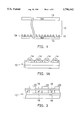
FIG. 1 is the top view of the basic SOI wafer carrying the memory array region together with the field oxides for the flash memory device to be fabricated;
FIG. 1A is the cross-sectional view taken along the 1A--1A line of FIG. 1 that shows the SOI wafer at the completion of the formation of the field oxides;
FIG. 2 is the cross-sectional view taken at a location in the memory array region of FIG. 1;
FIG. 3A is a cross-sectional view that shows a layer of BPSG that covers the first polysilicon layers completely;
FIG. 3B shows the BPSG layer reflown to achieve planarity and etched back until the first polysilicon layers expose;
FIG. 4 is the top view of the SOI wafer identifying the locations of the stacked gates;
FIGS. 4A and 4B shows for the device configuration on the SOI wafer taken along the 4A--4A and 4B--4B lines respectively in FIG. 4;
FIG. 5 schematically shows the top view of the SOI wafer having a completely fabricated flash array for the device of the present invention;
FIGS. 5A, 5B and 5C are cross-sectional views taken along the 5A-5A', 5B-5B' and 5C-5C' lines respectively in the top view of the fabricated SOI wafer shown in FIG. 5;
FIG. 6 is a perspective view of the fabricated flash array of the present invention showing the spatial characteristics of the device's structural configuration;
FIG. 7A schematically shows the structural configuration of one memory cell unit of the flash array of the present invention;
FIG. 7B shows the corresponding equivalent circuit symbol of the memory cell unit of the flash array of FIG. 7A; and
FIG. 8 schematically shows, in perspective manner, the connection of a group of memory cell units arranged in a portion of the flash array of the device of the present invention.
For the fabrication of the compact contactless flash array for the EEPROM device in accordance with a preferred process of the present invention, the starting material may be, for example, a <100> oriented p-type SOI wafer. The process is described in the depicted procedural steps outlined below. Note that the dimensions of the component configuration shown in the drawing for the description of the present invention are not drawn to the exact scale. The drawings are prepared to schematically exemplify the characteristics of the present invention, rather than showing the precise relative dimensions therein.
Step 1
Field oxide layers for the flash array are first grown over the surface of an SOI wafer.
FIG. 1 is the top view of the basic SOI wafer carrying the memory array region 12, together with the field oxides 14, for the flash memory device to be fabricated. To form the field oxide layers 14 for the memory cells in the memory array region 12, a layer of pad oxide (not shown in FIG. 1) with a thickness of about 200 to 400 Å is first grown over the surface of the SOI wafer, followed by the deposition of a nitride layer (not shown in FIG. 1) having a thickness of about 500 to 1,000 Å. The nitride layer is then patterned, and the photoresist then removed. Afterwards, field oxide layers 14 having a thickness of about 4,000 to 5,000 Å are grown under a temperature of about 900° to 950° C. utilizing the patterned nitride layer as the shielding mask. Then, after the formation of the field oxide layers 14, the nitride and pad oxide layers are removed. FIG. 1A shows the cross-sectional view of the SOI wafer 10 at the completion of this procedural step that reveals the cross section of the field oxide layer 14. Note that FIG. 1 shows the top view of the SOI wafer with the field oxide layers for the flash array being fabricated while FIG. 1A is the cross-sectional view taken along the 1A--1A line in FIG. 1.
Step 2
Gate oxide is grown followed by first polysilicon deposition, floating gates are formed by patterning the first polysilicon layer, and source/drain buried bitlines for the flash array are formed.
As is seen in FIG. 2, a layer of gate oxide 16 with a thickness of about 60 to 100 Å is grown at the appropriate location within the flash array region 12 (FIG. 1) on the SOI wafer, after which a first polysilicon layer with a thickness of about 1,500 Å is deposited. The first polysilicon layer is then patterned into the first polysilicon layers 20 in a photolithography procedure, followed by arsenic implantation at an energy level of about 25 KeV, achieving a dose of about 3E15/cm2 to form n+ buried bitlines 18. Then photoresist employed in the photolithography procedure is removed, followed by the surface reoxidation of the first polysilicon layers 20 at the temperature of about 900° to 950° C., resulting in a layer of oxide having a thickness of about 100 to 200 Å for the sake of sealing. Note that the cross-sectional view of FIG. 2 depicts the SOI wafer configuration at a different location from that shown in FIG. 1A.
Step 3
A first BPSG (borophosphosilicate glass) layer is deposited followed by reflow and etch back.
As is seen in FIG. 3A, a layer of BPSG 22 with a thickness of about 5,000 to 8,000 Å is then deposited in, for example, a low temperature oxide (LTO) deposition procedure in order to cover the first polysilicon layers 20 completely. Afterwards, the BPSG layer 22 is then reflown to achieve planarity and etched back until the first polysilicon layers 20 expose themselves, as is seen in FIG. 3B. Note that the cross-sectional view of FIGS. 3A and 3B are taken along the same location with that of FIG. 2 described in the previous procedural step.
Step 4
An oxide-nitride-oxide (ONO) layer is formed. A second polysilicon layer with in-situ dope is then deposited. A WSix layer is then formed.
As is seen in FIG. 4A, an ONO layer 24 with a thickness of about 100 to 150 Å is formed by means of, for example, first reoxidizing the first polysilicon layers 20 shown in FIG. 3B, followed by the deposition of a nitride layer having a thickness of about 50 to 100 Å, and then reoxidizing the deposited nitride subsequently to form the top oxide layer having a thickness of about 50 to 100 Å for the ONO configuration 24. A second polysilicon layer having a thickness of about 1,500 Å is then deposited atop the ONO configuration 24 with arsenic in-situ doping achieving a dose of about 5E15/cm2. This results in an n+ second polysilicon layer 26 as shown in the drawing. Then, a WSix layer 28 is formed further atop in order to reduce the resistance of the n+ second polysilicon layer 26. Note that the cross-sectional view of FIG. 4A is taken along the 4A--4A line in the top view FIG. 4 for the device configuration on the SOI wafer up to this stage. This cross-cutting reveals the stacked gates 34 (FIG. 4) for the memory cells in the flash array region 12 (FIG. 1).
Step 5
Stacked gates for the flash array are formed by patterning into the WSix, second polysilicon and oxide-nitride-oxide layers.
Stacked gates are then defined by, for example, plasma etching to remove unwanted portions of the WSix, second polysilicon, ONO and first polysilicon layers 28, 26, 24 and 20 respectively, followed by a reoxidation procedure at the temperature of about 900° to 950° C. to seal the stacked gate with an oxide layer having a thickness of 100 to 200 Å (not shown in the drawing). The sealing of the formed stacked gates facilitates the securing of device reliability in terms of reduced leakage current between floating gates and other regions. FIG. 4B is the cross-sectional view taken along the 4B--4B line in FIG. 4 that shows the SOI wafer configuration up to this fabrication stage. As is seen in FIG. 4B, all the WSix, second polysilicon, ONO and first polysilicon layers 28, 26, 24 and 20 respectively that are not relevant to the areas defined by stacked gates 34 have all been removed in the plasma etching procedure described above, and the BPSG layers 22 are directly exposed.
Step 6
Stacked gates are covered with a second BPSG layer.
A BPSG layer 30 shown in FIG. 5A with thickness of about 10,000 to 14,000 Å is then deposited to cover stacked gates completely which is subsequently reflown and etched back to achieve planarity. Each of the formed BPSG layers that covers the corresponding stacked gates has a thickness of about 8,000 to 12,000 Å that stacks atop the corresponding WSix layers 28 (FIG. 4A).
Step 7
Contact openings for the source/drain buried lines and n+ second polysilicon word lines are formed.
FIG. 5 schematically shows the top view of the SOI wafer having a completely fabricated flash array for the device of the present invention. As is seen in FIG. 5, contact openings 32 for n+ source/drain buried-lines are then opened by etching for, for example, every 16 or more flash cells, meanwhile, contact opening 32 for every n+ second polysilicon word lines are performed simultaneously. Thus the subsequently low resistive metal 36 shown in FIG. 5A can efficiently reduce the resistance of n+ buries source/drain diffusion lines by connection of both parallelly. Here the low resistance enhances the read current of flash cells and thereby improves read speed. On the other hand, body lines may have their contact openings 32 opened around the flash memory arrays.
Step 8
Metal lines leading into the contact openings are formed for interconnecting the memory cells in the flash array with relevant peripheral control circuits.
Step 8 generally concludes the process for the fabrication of the compact contactless flash array for EEPROM semiconductor devices in accordance with the preferred embodiment of the present invention. To describe the structural configuration of the compact contactless flash array of the present invention in further detail, three cross sectional views FIGS. 5A, 5B and 5C are taken along the 5A-5A', 5B-5B' and 5C-5C' lines respectively in the top view of the fabricated SOI wafer shown in FIG. 5. These three depicted cross-sectional views, which include the cross sections of the stacked gates, the region between consecutive stacked gates, and the field oxide at the periphery of the flash array region, are helpful in the understanding of the characteristics of the structural configuration of the flash array of the present invention, as well as the functional characteristics it can achieve.
In addition to the cross-sectional views FIGS. 5A, 5B and 5C, a perspective view of the fabricated flash array of the present invention is also shown in FIG. 6 to further demonstrate the spatial characteristics of the device's structural configuration. Simultaneous reference to the drawings of FIG. 5, FIGS. 5A, 5B and 5C and FIG. 6 will help identify the relative spatial relationships of the components for the construction of the flash array of the present invention.
FIG. 7A of the drawing schematically shows the structural configuration of one memory cell unit of the flash array of the present invention, while FIG. 7B shows the corresponding equivalent circuit symbol thereof. As is seen in FIGS. 7A and 7B, each of the fabricated memory cell unit includes a pair of n+ source/drain buried lines S and D respectively, a body line B, and a stacked gate G that generally includes a first polysilicon layer, an ONO configuration and a second polysilicon layer. The pair of n+ source/drain buried lines sandwiches the body line B, and the stacked gate G directly sits atop the body line B.
FIG. 8 schematically shows, in perspective manner, the connection of a group of memory cell units arranged in a portion of the flash array of the device of the present invention. In the drawing, circuit symbol of FIG. 7B has been employed to schematically exemplify the configuration of an array of memory cell units for the present invention. As is seen, a set of memory cell units may be cascaded in a row (or column) that have their stacked gates G all tied together and triggered by a word line signal Ga (or, Gb or Gc). Similarly, another set of memory cell units may be cascaded in a column (or row) that have their sources/drains S and D, as well as body lines B tied together respectively and be controlled by the body line signal B1 (or B2). In the arrangement shown in FIG. 8, each row (or column) of the memory cell units in the array may be directly addressed in either the read, erase or program mode via the selection of the attached metal line, such as the one exemplified by metal I that controls the body line B1 (or B2) and the word line Ga (or Gb or Gc).
Thus, in the flash array configuration of the present invention, each of the compact cells may share its source/drain with adjacent cells. The body lines isolated by source/drain lines allow for the flash memory cells of the present invention to make use of the FN (Fowler-Nordheim) tunneling effect between the floating gate and the substrate to implement both the programming and erasing operation. Due to the use of SOI wafer, the substrate portion of each of the adjacent cells is isolated by source and drain. By setting the voltage difference between substrate and gate, cell programming and erase can be performed, as is exemplified in the table below.
In terms of the applied electric potential at the control terminals of each of the memory cell units, Table 1 below lists such a control scheme for the read, erase and program of selected number of memory cells, assuming the activation of word line Ga and body line B1 in the array of FIG. 8.
              TABLE 1
______________________________________
Single cell
Operation Program     Erase       Read
______________________________________
G.sub.a   V.sub.ppt (13 V)
                      V.sub.BB2 (-13 V)
                                  V.sub.CG (5 V)
S.sub.1   0 V         Floating    0 V
B.sub.1   V.sub.BB1 (-7 V)
                      7 V         0 V
D.sub.1 = D.sub.2
          0 V         Floating    V.sub.D (1 V)
B.sub.2   0 V         0 V         0 V
S.sub.2   0 V         0 V         0 V
G.sub.b /G.sub.c
          0 V         0 V         0 V
______________________________________
When compared to the flash array of the prior art, the present invention is advantageously distinguishable in that the body line of the memory cell units of the present invention is being isolated by the surrounding buried n+ source/drain lines and the SiO2 layer of the SOI wafer. This allows the memory cells of the flash array of the present invention to be erased and programmed utilizing the body line and word line in an FN (Fowler-Nordheim) tunneling effect.
A majority of prior flash array memory cell configurations, on the other hand, would have to rely on the drain, source and word line thereof in a hot carrier transport mode to implement the memory cell programming. In the continuous trend of device dimensional scaling down for the improvement of memory density, the short channel effect that is inevitable in the prior art devices which rely on hot carrier program/erase operations constitutes a serious drawback when compared to the characteristics of the flash array of the present invention.
While the present invention has been described by way of example and in terms of preferred embodiments, it is to be understood that the invention need not be limited to the disclosed embodiments. On the contrary, it is intended to cover various modifications and similar arrangements included within the spirit and scope of the appended claims, the scope of which should be accorded the broadest interpretation so as to encompass all such modifications and similar structures.
Claims (10)
1. A compact contactless flash memory array for semiconductor EEPROM devices comprising a plurality of memory cell units,
wherein each of said cell units includes a body line, source and drain lines and a stacked gate constructed over a silicon-on-insulator wafer, and wherein:
said source and drain lines are buried lines;
said body line is isolated by surrounding buried source/drain lines and a SiO2 layer of said silicon-on-insulator wafer;
said stacked gate including a first polysilicon layer, an oxide-nitride-oxide configuration and a second polysilicon layer; and
said source and drain buried lines sandwiches said body line, and said stacked gate substantially sits directly atop said body line.
2. The compact contactless flash memory array of claim 1 further comprises field oxide layers having a thickness of about 4,000 to 5,000 Å grown under a temperature of about 900° to 950° C. utilizing patterned nitride layer as the shielding mask wherein
a layer of pad oxide with a thickness of about 200 to 400 Å grown over the surface of said silicon-on-insulator wafer; and
a nitride layer having a thickness of about 500 to 1,000 Å deposited on said layer of pad oxide and patterned.
3. The compact contactless flash memory array of claim 1 further comprises gate oxide layers, floating gates and source/drain buried bitlines wherein
said gate oxide layers are grown to have a thickness of about 60 to 100 Å;
said source/drain buried bitlines are formed by depositing a first polysilicon layer with a thickness of about 1,500 Å;
said first polysilicon layer is patterned and then implanted with arsenic ions at an energy level of about 25 KeV, achieving a dose of about 3E15/cm2 to form n+ type of said source/drain buried bitlines; and
surface of said first polysilicon layers are reoxidized at the temperature of about 900° to 950° C. to provide a layer of oxide having a thickness of about 100 to 200 Å.
4. The compact contactless flash memory array of claim 1 further comprises a first BPSG layer wherein
said first BPSG layer is deposited to have a thickness of about 5,000 to 8,000 Å in a low temperature oxide (LTO) deposition procedure for covering said first polysilicon layers completely; and
said first BPSG layer is reflown to achieve planarity and etched back until said first polysilicon layers expose.
5. The compact contactless flash memory array of claim 1 further comprises an oxide-nitride-oxide layer, a second polysilicon layer deposited with in-situ dope, and a WSix layer wherein
said oxide-nitride-oxide layer is formed to have a thickness of about 100 to 150 Å by first reoxidizing said first polysilicon layers, followed by the depositing a nitride layer having a thickness of about 50 to 100 Å, and then reoxidizing said deposited nitride subsequently to form the top oxide layer having a thickness of about 50 to 100 Å; and
said second polysilicon layer is formed to have a thickness of about 1,500 Å by depositing atop said oxide-nitride-oxide layer with arsenic in-situ doping achieving a dose of about 5E15/cm2 to form an n+ second polysilicon layer.
6. The compact contactless flash memory array of claim 5 further comprises stacked gates wherein
unwanted portions of said WSix, second polysilicon, oxide-nitride-oxide and first polysilicon layers are removed and pattern defined with plasma etching; and
said stacked gates are sealed by a reoxidation at the temperature of about 900° to 950° C.
7. The compact contactless flash memory array of claim 5, wherein said stacked gates are covered with a second BPSG layer formed by depositing a BPSG layer having a thickness of about 10,000 to 14,000 Å and reflowing and etching back the BPSG layer to achieve planarity and have a thickness of about 8,000 to 12,000 Å.
8. The compact contactless flash memory array of claim 1 further comprises contact openings formed for said source/drain buried lines and said n+ second polysilicon word lines wherein
every 16 or more of said flash cells are etched for n+ source/drain buried lines; and
said contact openings are opened around said flash memory arrays for body lines; and said contact openings are opened for every said n+ second polysilicon word lines.
9. The compact contactless flash memory array of claim 1 further comprises metal lines leading into said contact openings for interconnecting the memory cells in said flash memory array with peripheral control circuits of said semiconductor EEPROM devices.
10. The compact contactless flash memory array of claim 1, further comprises passivation formed for protecting said flash memory array.
Applications Claiming Priority (2)
| Application Number | Priority Date | Filing Date | Title |
|---|---|---|---|
| TW085106473A TW428319B (en) | 1996-05-31 | 1996-05-31 | High-density contactless flash memory on silicon above an insulator and its manufacturing method |
| TW85106473 | 1996-05-31 |
Publications (1)
| Publication Number | Publication Date |
|---|---|
| US5796142A true US5796142A (en) | 1998-08-18 |
Family
ID=21625266
Family Applications (2)
| Application Number | Title | Priority Date | Filing Date |
|---|---|---|---|
| US08/786,908 Expired - Lifetime US5796142A (en) | 1996-05-31 | 1997-01-22 | SOI compact contactless flash memory cell |
| US08/789,202 Expired - Lifetime US5885868A (en) | 1996-05-31 | 1997-01-24 | Process for fabricating SOI compact contactless flash memory cell |
Family Applications After (1)
| Application Number | Title | Priority Date | Filing Date |
|---|---|---|---|
| US08/789,202 Expired - Lifetime US5885868A (en) | 1996-05-31 | 1997-01-24 | Process for fabricating SOI compact contactless flash memory cell |
Country Status (2)
| Country | Link |
|---|---|
| US (2) | US5796142A (en) |
| TW (1) | TW428319B (en) |
Cited By (11)
| Publication number | Priority date | Publication date | Assignee | Title |
|---|---|---|---|---|
| US6162684A (en) * | 1999-03-11 | 2000-12-19 | Advanced Micro Devices, Inc. | Ammonia annealed and wet oxidized LPCVD oxide to replace ono films for high integrated flash memory devices |
| US20050179079A1 (en) * | 2004-02-18 | 2005-08-18 | Koucheng Wu | Nor-type channel-program channel-erase contactless flash memory on SOI |
| US20060245251A1 (en) * | 2005-05-02 | 2006-11-02 | Kabushiki Kaisha Toshiba | Semiconductor memory device |
| US20060279991A1 (en) * | 2005-06-11 | 2006-12-14 | Seoul National University Industry Foundation | Nand type flash memory array and method for operating the same |
| US20140159156A1 (en) * | 2007-11-29 | 2014-06-12 | Yuniarto Widjaja | Compact Semiconductor Memory Device Having Reduced Number of Contacts, Methods of Operating and Methods of Making |
| US9391079B2 (en) | 2007-11-29 | 2016-07-12 | Zeno Semiconductor, Inc. | Compact semiconductor memory device having reduced number of contacts, methods of operating and methods of making |
| US9601493B2 (en) | 2006-11-29 | 2017-03-21 | Zeno Semiconductor, Inc | Compact semiconductor memory device having reduced number of contacts, methods of operating and methods of making |
| US20170133391A1 (en) * | 2014-06-20 | 2017-05-11 | Floadia Corporation | Non-Volatile Semiconductor Memory Device |
| US9704870B2 (en) | 2010-03-02 | 2017-07-11 | Zeno Semiconductors, Inc. | Compact semiconductor memory device having reduced number of contacts, methods of operating and methods of making |
| US9922981B2 (en) | 2010-03-02 | 2018-03-20 | Zeno Semiconductor, Inc. | Compact semiconductor memory device having reduced number of contacts, methods of operating and methods of making |
| US10461084B2 (en) | 2010-03-02 | 2019-10-29 | Zeno Semiconductor, Inc. | Compact semiconductor memory device having reduced number of contacts, methods of operating and methods of making |
Families Citing this family (3)
| Publication number | Priority date | Publication date | Assignee | Title |
|---|---|---|---|---|
| US6252275B1 (en) * | 1999-01-07 | 2001-06-26 | International Business Machines Corporation | Silicon-on-insulator non-volatile random access memory device |
| US6512263B1 (en) | 2000-09-22 | 2003-01-28 | Sandisk Corporation | Non-volatile memory cell array having discontinuous source and drain diffusions contacted by continuous bit line conductors and methods of forming |
| DE10127350C1 (en) * | 2001-06-06 | 2003-02-13 | Infineon Technologies Ag | Semiconductor structure with buried conductor tracks and method for electrical contacting of the buried conductor tracks |
Citations (2)
| Publication number | Priority date | Publication date | Assignee | Title |
|---|---|---|---|---|
| US5075245A (en) * | 1990-08-03 | 1991-12-24 | Intel Corporation | Method for improving erase characteristics of buried bit line flash EPROM devices without using sacrificial oxide growth and removal steps |
| US5617351A (en) * | 1992-03-12 | 1997-04-01 | International Business Machines Corporation | Three-dimensional direct-write EEPROM arrays and fabrication methods |
Family Cites Families (7)
| Publication number | Priority date | Publication date | Assignee | Title |
|---|---|---|---|---|
| EP0528564A2 (en) * | 1991-08-20 | 1993-02-24 | National Semiconductor Corporation | Self-aligned stacked gate EPROM cell using tantalum oxide control gate dielectric |
| US5210047A (en) * | 1991-12-12 | 1993-05-11 | Woo Been Jon K | Process for fabricating a flash EPROM having reduced cell size |
| US5397726A (en) * | 1992-02-04 | 1995-03-14 | National Semiconductor Corporation | Segment-erasable flash EPROM |
| US5246874A (en) * | 1992-06-02 | 1993-09-21 | National Semiconductor Corporation | Method of making fast access AMG EPROM |
| US5364808A (en) * | 1994-02-07 | 1994-11-15 | United Micro Electronics Corporation | Method of making a buried bit line DRAM cell |
| US5494837A (en) * | 1994-09-27 | 1996-02-27 | Purdue Research Foundation | Method of forming semiconductor-on-insulator electronic devices by growing monocrystalline semiconducting regions from trench sidewalls |
| US5661060A (en) * | 1994-12-28 | 1997-08-26 | National Semiconductor Corporation | Method for forming field oxide regions |
-
1996
- 1996-05-31 TW TW085106473A patent/TW428319B/en not_active IP Right Cessation
-
1997
- 1997-01-22 US US08/786,908 patent/US5796142A/en not_active Expired - Lifetime
- 1997-01-24 US US08/789,202 patent/US5885868A/en not_active Expired - Lifetime
Patent Citations (2)
| Publication number | Priority date | Publication date | Assignee | Title |
|---|---|---|---|---|
| US5075245A (en) * | 1990-08-03 | 1991-12-24 | Intel Corporation | Method for improving erase characteristics of buried bit line flash EPROM devices without using sacrificial oxide growth and removal steps |
| US5617351A (en) * | 1992-03-12 | 1997-04-01 | International Business Machines Corporation | Three-dimensional direct-write EEPROM arrays and fabrication methods |
Non-Patent Citations (4)
| Title |
|---|
| "A NAND Structured Cell With A New Programming Technology For Highly Reliable 5-V Only Flash EEPROM," 1990 Symposium on VLSI Technology, pp. 129-130. |
| "A Novel Memory Cell Using Flash Array Contactless EPROM (FACE) Technology," 1990 IEDM, pp. 90-94. |
| A NAND Structured Cell With A New Programming Technology For Highly Reliable 5 V Only Flash EEPROM, 1990 Symposium on VLSI Technology, pp. 129 130. * |
| A Novel Memory Cell Using Flash Array Contactless EPROM (FACE) Technology, 1990 IEDM, pp. 90 94. * |
Cited By (28)
| Publication number | Priority date | Publication date | Assignee | Title |
|---|---|---|---|---|
| US6162684A (en) * | 1999-03-11 | 2000-12-19 | Advanced Micro Devices, Inc. | Ammonia annealed and wet oxidized LPCVD oxide to replace ono films for high integrated flash memory devices |
| US7495283B2 (en) | 2004-02-18 | 2009-02-24 | Koucheng Wu | Nor-type channel-program channel-erase contactless flash memory on SOI |
| US20060018164A1 (en) * | 2004-02-18 | 2006-01-26 | Koucheng Wu | Nor-type channel-program channel-erase contactless flash memory on SOI |
| US7042044B2 (en) | 2004-02-18 | 2006-05-09 | Koucheng Wu | Nor-type channel-program channel-erase contactless flash memory on SOI |
| US20090029511A1 (en) * | 2004-02-18 | 2009-01-29 | Koucheng Wu | NOR-type channel-program channel-erase contactless flash memory on SOI |
| US20050179079A1 (en) * | 2004-02-18 | 2005-08-18 | Koucheng Wu | Nor-type channel-program channel-erase contactless flash memory on SOI |
| US20060245251A1 (en) * | 2005-05-02 | 2006-11-02 | Kabushiki Kaisha Toshiba | Semiconductor memory device |
| US7408811B2 (en) * | 2005-05-02 | 2008-08-05 | Kabushiki Kaisha Toshiba | NAND-type flash memory on an SOI substrate with a carrier discharging operation |
| US20090010074A1 (en) * | 2005-05-02 | 2009-01-08 | Kabushiki Kaisha Toshiba | Semiconductor memory device |
| US7791948B2 (en) | 2005-05-02 | 2010-09-07 | Kabushiki Kaisha Toshiba | Channel carrier discharging in a NAND flash memory on an insulating substrate or layer |
| US20060279991A1 (en) * | 2005-06-11 | 2006-12-14 | Seoul National University Industry Foundation | Nand type flash memory array and method for operating the same |
| US7502262B2 (en) * | 2005-06-11 | 2009-03-10 | Seoul National University Industry Foundation | NAND type flash memory array and method for operating the same |
| US9601493B2 (en) | 2006-11-29 | 2017-03-21 | Zeno Semiconductor, Inc | Compact semiconductor memory device having reduced number of contacts, methods of operating and methods of making |
| US9209188B2 (en) | 2007-11-29 | 2015-12-08 | Zeno Semiconductor, Inc. | Compact semiconductor memory device having reduced number of contacts, methods of operating and methods of making |
| US9001581B2 (en) * | 2007-11-29 | 2015-04-07 | Zeno Semiconductor Inc. | Compact semiconductor memory device having reduced number of contacts, methods of operating and methods of making |
| US9391079B2 (en) | 2007-11-29 | 2016-07-12 | Zeno Semiconductor, Inc. | Compact semiconductor memory device having reduced number of contacts, methods of operating and methods of making |
| US20140159156A1 (en) * | 2007-11-29 | 2014-06-12 | Yuniarto Widjaja | Compact Semiconductor Memory Device Having Reduced Number of Contacts, Methods of Operating and Methods of Making |
| US10461084B2 (en) | 2010-03-02 | 2019-10-29 | Zeno Semiconductor, Inc. | Compact semiconductor memory device having reduced number of contacts, methods of operating and methods of making |
| US9704870B2 (en) | 2010-03-02 | 2017-07-11 | Zeno Semiconductors, Inc. | Compact semiconductor memory device having reduced number of contacts, methods of operating and methods of making |
| US9922981B2 (en) | 2010-03-02 | 2018-03-20 | Zeno Semiconductor, Inc. | Compact semiconductor memory device having reduced number of contacts, methods of operating and methods of making |
| US10056387B2 (en) | 2010-03-02 | 2018-08-21 | Zeno Semiconductor, Inc. | Compact semiconductor memory device having reduced number of contacts, methods of operating and methods of making |
| US10204908B2 (en) | 2010-03-02 | 2019-02-12 | Zeno Semiconductor, Inc. | Compact semiconductor memory device having reduced number of contacts, methods of operating and methods of making |
| US10347636B2 (en) | 2010-03-02 | 2019-07-09 | Zeno Semiconductor, Inc. | Compact semiconductor memory device having reduced number of contacts, methods of operating and methods of making |
| US10615163B2 (en) | 2010-03-02 | 2020-04-07 | Zeno Semiconductor, Inc. | Compact semiconductor memory device having reduced number of contacts, methods of operating and methods of making |
| US11037929B2 (en) | 2010-03-02 | 2021-06-15 | Zeno Semiconductor Inc. | Compact semiconductor memory device having reduced number of contacts, methods of operating and methods of making |
| US11488955B2 (en) | 2010-03-02 | 2022-11-01 | Zeno Semiconductor, Inc. | Compact semiconductor memory device having reduced number of contacts, methods of operating and methods of making |
| US20170133391A1 (en) * | 2014-06-20 | 2017-05-11 | Floadia Corporation | Non-Volatile Semiconductor Memory Device |
| US10680001B2 (en) * | 2014-06-20 | 2020-06-09 | Floadia Corporation | Non-volatile semiconductor memory device |
Also Published As
| Publication number | Publication date |
|---|---|
| US5885868A (en) | 1999-03-23 |
| TW428319B (en) | 2001-04-01 |
Similar Documents
| Publication | Publication Date | Title |
|---|---|---|
| US7015098B2 (en) | Methods and structure for an improved floating gate memory cell | |
| US5464999A (en) | Method for programming an alternate metal/source virtual ground flash EPROM cell array | |
| US5622881A (en) | Packing density for flash memories | |
| US5953254A (en) | Serial flash memory | |
| US6346725B1 (en) | Contact-less array of fully self-aligned, triple polysilicon, source-side injection, nonvolatile memory cells with metal-overlaid wordlines | |
| EP0780902B1 (en) | Nonvolatile semiconductor memory and method for fabricating the same | |
| KR100554089B1 (en) | Elimination of poly cap for easy poly1 contact for nand floating gate memory | |
| US6143606A (en) | Method for manufacturing split-gate flash memory cell | |
| US5796142A (en) | SOI compact contactless flash memory cell | |
| US5615152A (en) | Method of erasing a high density contactless flash EPROM array | |
| US5851879A (en) | Method for fabricating compact contactless trenched flash memory cell | |
| KR0144421B1 (en) | Manufacturing method of fresh E.P.Rom | |
| US20050164457A1 (en) | Non-volatile memory devices and methods of fabricating the same | |
| US6893921B2 (en) | Nonvolatile memories with a floating gate having an upward protrusion | |
| US6096604A (en) | Production of reversed flash memory device | |
| JP2004165182A (en) | Semiconductor device | |
| US5409854A (en) | Method for forming a virtual-ground flash EPROM array with floating gates that are self aligned to the field oxide regions of the array | |
| US5466624A (en) | Isolation between diffusion lines in a memory array | |
| US5576232A (en) | Fabrication process for flash memory in which channel lengths are controlled | |
| US6083791A (en) | Self-aligned stacked gate etch process for fabricating a two-transistor EEPROM cell | |
| US7227216B2 (en) | Mono gate memory device and fabricating method thereof | |
| US5998262A (en) | Method for manufacturing ETOX cell having damage-free source region | |
| US20060180850A1 (en) | Process for manufacturing a memory with local electrical contact between the source line and the well | |
| US20050045939A1 (en) | Split-gate memory cell, memory array incorporating same, and method of manufacture thereof | |
| KR19990006172A (en) | Ipyrom Cell |
Legal Events
| Date | Code | Title | Description |
|---|---|---|---|
| AS | Assignment |
Owner name: UNITED MICROELECTRONICS CORP., TAIWAN Free format text: ASSIGNMENT OF ASSIGNORS INTEREST;ASSIGNORS:LIN, RUEI-LING;HSU, CHING-HSIANG;HONG, GARY;REEL/FRAME:008402/0936 Effective date: 19961119 |
|
| STCF | Information on status: patent grant |
Free format text: PATENTED CASE |
|
| FPAY | Fee payment |
Year of fee payment: 4 |
|
| FPAY | Fee payment |
Year of fee payment: 8 |
|
| FPAY | Fee payment |
Year of fee payment: 12 |