US5796133A - Semiconductor device capacitor having lower electrodes separated by low dielectric spacer material - Google Patents
Semiconductor device capacitor having lower electrodes separated by low dielectric spacer material Download PDFInfo
- Publication number
- US5796133A US5796133A US08/782,827 US78282797A US5796133A US 5796133 A US5796133 A US 5796133A US 78282797 A US78282797 A US 78282797A US 5796133 A US5796133 A US 5796133A
- Authority
- US
- United States
- Prior art keywords
- semiconductor device
- lower electrodes
- ferroelectric film
- over
- spacer
- Prior art date
- Legal status (The legal status is an assumption and is not a legal conclusion. Google has not performed a legal analysis and makes no representation as to the accuracy of the status listed.)
- Expired - Lifetime
Links
Images


Classifications
-
- H—ELECTRICITY
- H01—ELECTRIC ELEMENTS
- H01L—SEMICONDUCTOR DEVICES NOT COVERED BY CLASS H10
- H01L28/00—Passive two-terminal components without a potential-jump or surface barrier for integrated circuits; Details thereof; Multistep manufacturing processes therefor
- H01L28/40—Capacitors
- H01L28/55—Capacitors with a dielectric comprising a perovskite structure material
-
- H—ELECTRICITY
- H01—ELECTRIC ELEMENTS
- H01L—SEMICONDUCTOR DEVICES NOT COVERED BY CLASS H10
- H01L28/00—Passive two-terminal components without a potential-jump or surface barrier for integrated circuits; Details thereof; Multistep manufacturing processes therefor
- H01L28/40—Capacitors
- H01L28/60—Electrodes
-
- H—ELECTRICITY
- H10—SEMICONDUCTOR DEVICES; ELECTRIC SOLID-STATE DEVICES NOT OTHERWISE PROVIDED FOR
- H10B—ELECTRONIC MEMORY DEVICES
- H10B12/00—Dynamic random access memory [DRAM] devices
- H10B12/01—Manufacture or treatment
- H10B12/02—Manufacture or treatment for one transistor one-capacitor [1T-1C] memory cells
- H10B12/03—Making the capacitor or connections thereto
- H10B12/033—Making the capacitor or connections thereto the capacitor extending over the transistor
-
- H—ELECTRICITY
- H10—SEMICONDUCTOR DEVICES; ELECTRIC SOLID-STATE DEVICES NOT OTHERWISE PROVIDED FOR
- H10B—ELECTRONIC MEMORY DEVICES
- H10B12/00—Dynamic random access memory [DRAM] devices
- H10B12/30—DRAM devices comprising one-transistor - one-capacitor [1T-1C] memory cells
- H10B12/31—DRAM devices comprising one-transistor - one-capacitor [1T-1C] memory cells having a storage electrode stacked over the transistor
-
- H—ELECTRICITY
- H10—SEMICONDUCTOR DEVICES; ELECTRIC SOLID-STATE DEVICES NOT OTHERWISE PROVIDED FOR
- H10B—ELECTRONIC MEMORY DEVICES
- H10B53/00—Ferroelectric RAM [FeRAM] devices comprising ferroelectric memory capacitors
Definitions
- FIGS. 2A to 2E are sectional views that illustrate a method for manufacturing this capacitor.
- a semiconductor device having a capacitor with a spacer formed on the side surfaces of plural lower electrodes.
- the spacer comprises a material with a low dielectric constant.
- a ferroelectric film is formed on the lower electrodes, and an upper electrode is formed on the ferroelectric film.
- FIGS. 3 to 6 are sectional views for illustrating a method for manufacturing a semiconductor device comprising a ferroelectric film capacitor according to a first embodiment of the present invention
Abstract
In a semiconductor device having a ferroelectric capacitor and manufacturing method thereof, a spacer comprising a low dielectric material is formed on the side surfaces of a plurality of lower electrodes separated into each cell unit, and a ferroelectric film is formed on the lower electrodes whereon the low dielectric material spacer is formed, and an upper electrode is formed on the ferroelectric film, to thereby prevent an error which may be caused between the adjacent lower electrodes.
Description
This is a continuation of application Ser. No. 08/187,037, filed Jan. 27, 1994, which was now abandoned.
The present invention relates to a semiconductor device and a method for manufacturing the same, and more particularly, to a semiconductor device and a method for manufacturing the same which uses a ferroelectric film as the dielectric film of a capacitor.
The integration of dynamic random access memory (DRAM) devices has been increasing in recent years, and many methods for increasing capacitance within a limited cell area have been proposed. These methods can be largely divided into two groups: one in which the physical structural characteristics of the capacitor are improved, and another in which the capacitor comprises a material having a high dielectric constant.
Where the capacitor structure has been improved, the effective area of the capacitor has been increased by forming a three-dimensional storage electrode. Here, however, design rule limitations and complicated manufacturing processes impede the increase of capacitance.
On the other hand, where a material having a high dielectric constant is used as the dielectric film of the capacitor, capacitance is not limited by design rule and can be increased more easily.
Recently, it has been proposed to use a ferroelectric material as the dielectric film. Unlike the previously existing oxide, silicon nitride or tantalum pentoxide (Ta2 O5) films, a ferroelectric material is a material which exhibits spontaneous polarization, and generally has a high dielectric constant of at least 1,000. When the ferroelectric material is used as the dielectric film, the thickness of an equivalent oxide film can be reduced, for example, to 10 Å or less, even though the ferroelectric material is formed to a thickness of only several thousand angstroms. Furthermore, due to the spontaneous polarization phenomenon, a dielectric film comprising a ferroelectric material can be used for nonvolatile memory devices as well as for DRAMs.
In addition, PZT (PbZrTiO3), BST (BaSrTiO3) and the like have high dielectric constants and ferroelectric characteristics that differ according to their composite ratio. Therefore, these materials have recently been popular as dielectric materials for DRAM capacitors. When such materials are used for the dielectric film, platinum is used for the electrode of the capacitor due to its great resistance to oxidation.
FIG. 1 is a sectional view of a semiconductor device having a ferroelectric film capacitor manufactured by a conventional method.
In FIG. 1, a transistor pair is formed in the active region defined by field oxide film 10 of a semiconductor substrate 100. The transistors share a drain region 7, and each comprise a source region 5 and a gate electrode 15. A bit line 20 is connected to drain region 7, and contact holes for exposing predetermined portions of each source region 5 are formed thereabove.
Each contact hole is filled with a conductive plug 25 and the capacitors' lower electrodes, each consisting of a titanium layer 30 and platinum layer 35, are formed on each plug. A ferroelectric thin film 40 is formed over the lower electrodes, and an upper electrode 50 is formed on ferroelectric thin film 40.
In a capacitor manufactured according to the conventional method described above, the film can be weakened at the sharp edges of the lower electrode (e.g., see area "B" of FIG. 1) when the ferroelectric film is formed after lower electrode formation. In addition, because the dielectric constant of a ferroelectric film is very large, roughly from 1,000 to 10,000, there is a high possibility that errors will occur between the adjacent capacitors through the ferroelectric film disposed between the adjacent lower electrodes (see area "A" of FIG. 1).
In 1991, Kuniaki Koyama et al. disclosed a new method for manufacturing a capacitor in order to solve the problems described above (see IEDM '91, "A Stacked Capacitor with (Bax Sr1-x)TiO3 for 256M DRAMs"). FIGS. 2A to 2E are sectional views that illustrate a method for manufacturing this capacitor.
Referring to FIG. 2A, an insulating layer 102 is formed on semiconductor substrate 100, and a contact hole 105 is formed by etching a predetermined portion of insulating layer 102. Then, impurity-doped polysilicon is deposited over the entire resultant structure, and fills contact hole 105. The structure is subsequently etched back in a manner which allows contact hole 105 to remain filled with polysilicon 110.
Referring to FIG. 2B, a tantalum layer and a platinum layer are sequentially sputtered on the resultant structure, each to a thickness of 500 Å. Both layers are then patterned by a dry-etching process to form a platinum pattern 125 and a tantalum pattern 120, which constitute a lower electrode.
Referring to FIG. 2C, (Ba0.5 Sr0.5)TiO3 is deposited over the entire resultant structure by RF magnetron sputtering, to thereby form a ferroelectric film 130 having a thickness of 700-2,000 Å.
Referring to FIG. 2D, a chemical vapor deposition (CVD) oxide film having a thickness of 1,000 Å is formed over the entire resultant structure. The structure is subsequently etched anisotropically, to thereby form a spacer 135 which reduces leakage current caused by the poor step coverage of ferroelectric film 130.
Referring to FIG. 2E, a titanium nitride (TiN) layer 140 forms an upper electrode having a thickness of 1,000 Å and is deposited across the entire resultant structure.
A capacitor manufactured by the above method forms a CVD oxide film spacer whose breakdown resistance is excellent even at the weak portions of the ferroelectric film, and thus has a very low leakage current and a stable breakdown resistance distribution.
However, due to the very high dielectric constant of the ferroelectric film, the possibility that an error will be caused between the adjacent capacitors still remains.
Accordingly, it is a first object of the present invention to provide a reliable semiconductor device having a spacer consisting of a low dielectric material between the adjacent capacitors. It is a second object of the present invention to provide a method especially suited for manufacturing the above described reliable semiconductor device.
To accomplish the first object of the present invention, there is provided a semiconductor device having a capacitor with a spacer formed on the side surfaces of plural lower electrodes. The spacer comprises a material with a low dielectric constant. A ferroelectric film is formed on the lower electrodes, and an upper electrode is formed on the ferroelectric film.
To accomplish the second object of the present invention, there is provided a method for manufacturing a semiconductor device having a capacitor, comprising the steps of: forming a plurality of lower electrodes from a conductive material; forming a spacer comprising a material with a low dielectric constant on the side surfaces of each lower electrode; forming a ferroelectric film over at least the spacer and lower electrodes; and forming an upper electrode on the ferroelectric film.
To accomplish another object of the present invention, there is provided a method for manufacturing a semiconductor device having a capacitor, comprising the steps of: forming a plurality of lower electrodes from a conductive material; providing a material having a low dielectric constant between the lower electrodes; forming a ferroelectric film over at least the lower electrodes and said material having a low dielectric constant; and forming an upper electrode on the ferroelectric film.
Accordingly, a spacer having a low dielectric constant is formed between each lower electrode, to thereby prevent the occurrence of errors between the adjacent capacitors.
The above objects and other advantages of the present invention will become more apparent in view of the following description of a preferred embodiment with reference to the attached drawings in which:
FIG. 1 is a sectional view showing a semiconductor device comprising a ferroelectric film capacitor manufactured by a conventional method;
FIGS. 2A to 2E are sectional views for illustrating a ferroelectric film capacitor manufactured by another conventional method;
FIGS. 3 to 6 are sectional views for illustrating a method for manufacturing a semiconductor device comprising a ferroelectric film capacitor according to a first embodiment of the present invention;
FIGS. 7 to 8 are sectional views for illustrating a method for manufacturing a semiconductor device comprising a ferroelectric film capacitor according to a second embodiment of the present invention; and
FIGS. 9 to 10 are sectional views for illustrating a method for manufacturing a semiconductor device comprising a ferroelectric film capacitor according to a third embodiment of the present invention.
The present invention will be explained in more detail with reference to the attached drawings.
FIGS. 3 to 6 are sectional views for illustrating a method for manufacturing a semiconductor device comprising a ferroelectric film capacitor according to a first embodiment of the present invention.
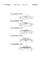
FIG. 3 shows the step of forming a contact hole and a conductive plug 25 on a semiconductor substrate 100 whereon a transistor pair is formed. Semiconductor substrate 100 has an isolation region and an active region as defined by field oxide film 10. A pair of transistors each have a source region 5, a gate electrode 15, and share a drain region 7 and a bit line 20 connected to the drain region. The transistors are formed on the active region of semiconductor substrate 100. Then, an insulating layer (not shown) is formed over the entire substrate 100. A planarization layer 23 is then formed over the entire resultant structure in order to planarize the uneven surface of substrate 100 created by the formation of the transistors and bit line. Then, planarization layer 23 and the insulating layer, are selectively etched at an area above the source regions 5 to form contact holes for connecting the source regions to lower electrodes. Then, as a conductive material, phosphorous-doped polysilicon is deposited on substrate 100 at least where the contact hole is formed, and then etched back so that the contact hole is filled with a conductive plug 25.
FIG. 4 shows the step of forming the lower electrodes of the capacitor. A titanium layer having a thickness of approximately 500 Å and a platinum layer having a thickness of 1,000 Å are sequentially formed by sputtering these substances over the entire resultant structure, including conductive plug 25. Then, a photoresist pattern (not shown) is formed on the platinum layer (upper layer) by coating, exposing and developing the photoresist so as to define each cell. Then, both layers are simultaneously etched using the photoresist pattern as a mask, to thereby form the capacitor's lower electrode which consists of platinum pattern 35 and titanium pattern 30. Then, the first photoresist pattern is removed. Here, tantalum can be used instead of titanium in the lower electrode.
FIG. 5 shows the step of forming a first spacer 45'. A material having a low dielectric constant, such as plasma-enhanced SiO2 (PE--SiO2), a CVD oxide film, silicon nitride (Six Ny), boro-nitride (BN), boro-phosphorous silicate glass (BPSG), phosphorous silicate glass (PSG), undoped silicate glass (USG) or boro-silicate glass (BSG) is deposited to a thickness of 1,500 Å to 2,000 Å on the resultant structure of FIG. 4. Then, the low dielectric material is etched anisotropically to form first spacer 45' on the side surfaces of the lower electrode.
FIG. 6 shows the step of forming a ferroelectric film 40 and an upper electrode 50. The ferroelectric material may comprise PZT, PbTiO3 (PLT), PbLaZrTiO3 (PLZT), SrTiO3 (STO), BST or LiNbO3 (LNO), and is deposited by a CVD method on the resultant structure of FIG. 5. As a result, ferroelectric film 40 is formed. Then, as a conductive material, platinum, TiN or aluminum is deposited on ferroelectric film 40 to form the capacitor's upper electrode.
FIGS. 7 to 8 are sectional views for illustrating a method for manufacturing a semiconductor device comprising a ferroelectric film capacitor according to a second embodiment of the present invention.
FIG. 7 shows the step of forming the lower electrodes of the capacitor and a second spacer 60. After forming the lower electrodes using the method explained with respect to FIGS. 3 and 4, a low dielectric material consisting of BN, BPSG, BSG or SiO2 is deposited to a thickness of approximately 2,000 Å to 10,000 Å over the resultant structure. Then, the low dielectric material is etched anisotropically so that second spacer 60 is formed on the side surface of the lower electrodes, which consist of platinum pattern 30 and titanium pattern 35. Second spacers 60 fills the space between the adjacent lower electrodes more than the spacers in the first embodiment.
FIG. 8 shows the step of sequentially forming ferroelectric film 40 and upper electrode 50 on lower electrodes having side surfaces provided with second spacer 60 using the method explained with respect to FIG. 7.
FIGS. 9 and 10 are sectional views for illustrating a method for manufacturing for a semiconductor device which comprises a ferroelectric film capacitor according to a third embodiment of the present invention.
FIG. 9 shows the step of forming the lower electrodes and a third spacer 70. After forming the lower electrodes using the method explained with respect to FIGS. 3 and 4, a low dielectric material such as BPSG, PSG or BSG is deposited to a thickness of approximately 2,000 Å to 10,000 Å over the entire resultant structure. Then, the low dielectric material is planarized by a high-temperature heat treatment process, and the resultant structure is etched anisotropically so that third spacer 70 is formed on the side surfaces of the lower electrode consists of platinum pattern 35 and titanium pattern 30. Third spacer 70 completely fills up the space between the adjacent lower electrodes so that the lower electrodes of each cell can be separated by a planarized surface.
FIG. 10 shows the step of then sequentially forming ferroelectric film 40 and upper electrode 50 on the lower electrodes using the method explained with respect to FIG. 6.
As described above, and according to embodiments of the present invention, a spacer comprising a low dielectric material is formed on the side surfaces of a capacitor's lower electrode so that errors which may be caused between the adjacent lower electrodes are prevented. In addition, the sharp edges of the lower electrodes are somewhat more rounded by the spacers, and as a result, the possibility that the ferroelectric film may be weakened in this area is reduced.
In addition, in all the above embodiments, since a spacer consisting of the low dielectric material is formed by a simple anisotropic etching process without the use of any additional masking, the problems associated with the prior art can be easily solved without added processing problems and without increasing production costs.
It is understood by those skilled in the art that the foregoing description is a preferred embodiment of the disclosed device and that various changes and modifications may be made in the invention without departing from the spirit and scope thereof.
Claims (16)
1. A semiconductor device having a capacitor, said semiconductor device comprising:
a plurality of lower electrodes each having side surfaces;
a spacer formed on each of the side surfaces of said lower electrodes, said spacer comprising a material having a low dielectric constant, and at least two of said spacers and corresponding lower electrodes forming rounded edges, the height of said spacers not exceeding the height of said lower electrodes;
a ferroelectric film formed over said plurality of lower electrodes and over said spacers, including over said rounded edges; and
an upper electrode formed over said ferroelectric film including the film formed over said rounded edges.
2. A semiconductor device according to claim 1, wherein said spacer comprises a material selected from the group comprising PE--SiO2, CVD oxide, Six Ny, BN, BPSG, PSG, USG and BSG.
3. A semiconductor device according to claim 1, wherein at least one space is formed between said electrodes, and wherein said material having a low dielectric constant fills said at least one space.
4. A semiconductor device according to claim 2, wherein at least one space is formed between said lower electrodes, and wherein said material having a low dielectric constant fills said at least one space.
5. The semiconductor device according to claim 1, wherein said ferroelectric film is formed on said plurality of lower electrodes, and further wherein said ferroelectric film is formed on said spacer.
6. The semiconductor device according to claim 1, wherein said upper electrode is formed on said ferroelectric film.
7. The semiconductor device according to claim 5, wherein said upper electrode is formed on said ferroelectric film.
8. The semiconductor device according to claim 1, further comprising:
a semiconductor substrate having an active region and a pair of transistors formed in said active region, said pair of transistors comprising a common drain region, gate regions and source regions;
a bit line connected to said common drain region; and
means for forming a conductive path between said lower electrodes and respective ones of said source regions;
and a planarization layer formed over said semiconductor substrate;
said plurality of lower electrodes being formed over said planarization layer.
9. A semiconductor device having a capacitor, said semiconductor device comprising:
at least two lower electrodes arranged to form a space therebetween, said electrodes including respective inner side surfaces, forming respective opposing sides of said space, and respective outer side surfaces;
a spacer material formed on each of said respective inner and outer side surfaces and at least partially filling said space, said spacer material having a low dielectric constant, and at least two of said spacers and corresponding lower electrodes forming rounded edges, the height of said spacers not exceeding the height of said lower electrodes;
a ferroelectric film formed over said at least two lower electrodes and over said spacer material, including over said rounded edges; and
at least one upper electrode formed over said ferroelectric film including the film formed over said rounded edges.
10. The semiconductor device according to claim 9, wherein said spacer material comprises a material selected from the group comprising PE--SiO2, CVD oxide, Six Ny, BN, BPSG, PSG, USG and BSG.
11. The semiconductor device according to claim 9, wherein said semiconductor device comprises a dynamic random access memory device.
12. The semiconductor device according to claim 9, wherein said ferroelectric film has a dielectric constant of at least 1,000.
13. The semiconductor device according to claim 9, wherein said ferroelectric film comprises a material selected from the group comprising PZT, PbTiO3 (PLT), PbLaZrTiO3 (PLZT), SrTiO3 (STO), BST, LiNbO3 (LNO).
14. The semiconductor device according to claim 9, further comprising:
a semiconductor substrate having an active region and a pair of transistors formed in said active region, said pair of transistors comprising a common drain region, gate regions and source regions;
a bit line connected to said common drain region; and
means for forming a conductive path between said lower electrodes and respective ones of said source regions;
and a planarization layer formed over said semiconductor substrate;
said plurality of lower electrodes being formed over said planarization layer.
15. The semiconductor device according to claim 1, wherein said rounded edges reduce the possibility that portions of said ferroelectric film over said rounded edges are weakened relative to other portions of said ferroelectric film.
16. The semiconductor device according to claim 9, wherein said rounded edges reduce the possibility that portions of said ferroelectric film over said rounded edges are weakened relative to other portions of said ferroelectric film.
Priority Applications (1)
| Application Number | Priority Date | Filing Date | Title |
|---|---|---|---|
| US08/782,827 US5796133A (en) | 1993-01-27 | 1997-01-13 | Semiconductor device capacitor having lower electrodes separated by low dielectric spacer material |
Applications Claiming Priority (4)
| Application Number | Priority Date | Filing Date | Title |
|---|---|---|---|
| KR1019930000963A KR950009813B1 (en) | 1993-01-27 | 1993-01-27 | Semiconductor device and manufacturing method thereof |
| KR1993963 | 1993-01-27 | ||
| US18703794A | 1994-01-27 | 1994-01-27 | |
| US08/782,827 US5796133A (en) | 1993-01-27 | 1997-01-13 | Semiconductor device capacitor having lower electrodes separated by low dielectric spacer material |
Related Parent Applications (1)
| Application Number | Title | Priority Date | Filing Date |
|---|---|---|---|
| US18703794A Continuation | 1993-01-27 | 1994-01-27 |
Publications (1)
| Publication Number | Publication Date |
|---|---|
| US5796133A true US5796133A (en) | 1998-08-18 |
Family
ID=19350001
Family Applications (2)
| Application Number | Title | Priority Date | Filing Date |
|---|---|---|---|
| US08/738,470 Expired - Lifetime US5834348A (en) | 1993-01-27 | 1996-10-30 | Method for manufacturing a semiconductor device having a ferroelectric capacitor |
| US08/782,827 Expired - Lifetime US5796133A (en) | 1993-01-27 | 1997-01-13 | Semiconductor device capacitor having lower electrodes separated by low dielectric spacer material |
Family Applications Before (1)
| Application Number | Title | Priority Date | Filing Date |
|---|---|---|---|
| US08/738,470 Expired - Lifetime US5834348A (en) | 1993-01-27 | 1996-10-30 | Method for manufacturing a semiconductor device having a ferroelectric capacitor |
Country Status (6)
| Country | Link |
|---|---|
| US (2) | US5834348A (en) |
| JP (1) | JP3384599B2 (en) |
| KR (1) | KR950009813B1 (en) |
| CA (1) | CA2113958C (en) |
| DE (1) | DE4402216C2 (en) |
| GB (1) | GB2274741B (en) |
Cited By (15)
| Publication number | Priority date | Publication date | Assignee | Title |
|---|---|---|---|---|
| US5933761A (en) * | 1998-02-09 | 1999-08-03 | Lee; Ellis | Dual damascene structure and its manufacturing method |
| US5998256A (en) * | 1996-11-01 | 1999-12-07 | Micron Technology, Inc. | Semiconductor processing methods of forming devices on a substrate, forming device arrays on a substrate, forming conductive lines on a substrate, and forming capacitor arrays on a substrate, and integrated circuitry |
| US6023101A (en) * | 1997-12-10 | 2000-02-08 | Mitsubishi Denki Kabushiki Kaisha | Semiconductor device and method for manufacturing the same |
| US6025277A (en) * | 1997-05-07 | 2000-02-15 | United Microelectronics Corp. | Method and structure for preventing bonding pad peel back |
| US6049103A (en) * | 1995-03-22 | 2000-04-11 | Mitsubishi Denki Kabushiki Kaisha | Semiconductor capacitor |
| US6300652B1 (en) * | 1995-11-22 | 2001-10-09 | Infineon Technologies Ag | Memory cell configuration and method for its production |
| US6300654B1 (en) * | 1999-04-30 | 2001-10-09 | Stmicroelectronics S.R.L. | Structure of a stacked memory cell, in particular a ferroelectric cell |
| US20020081852A1 (en) * | 2000-03-20 | 2002-06-27 | Sandhu Gurtej S. | Method to form etch and/or CMP stop layers |
| US6590250B2 (en) | 1997-11-25 | 2003-07-08 | Micron Technology, Inc. | DRAM capacitor array and integrated device array of substantially identically shaped devices |
| US20040058493A1 (en) * | 1999-04-30 | 2004-03-25 | Stmicroelectronics S.R.I. | Method of fabricating a ferroelectric stacked memory cell |
| US20040166627A1 (en) * | 2003-02-25 | 2004-08-26 | Lim Jae-Soon | Methods for forming a capacitor on an integrated circuit device at reduced temperatures |
| US20050041505A1 (en) * | 2000-10-17 | 2005-02-24 | Matsushita Electric Industrial Co., Ltd. | Ferroelectric memory and method for manufacturing the same |
| US20050133842A1 (en) * | 2002-11-18 | 2005-06-23 | Fujitsu Limited | Semiconductor device and fabrication method of a semiconductor device |
| US20050205907A1 (en) * | 2004-03-19 | 2005-09-22 | Isenberger Mark S | Memory circuit with spacers between ferroelectric layer and electrodes |
| US20080017894A1 (en) * | 2006-07-18 | 2008-01-24 | Thomas Happ | Integrated circuit with memory having a step-like programming characteristic |
Families Citing this family (28)
| Publication number | Priority date | Publication date | Assignee | Title |
|---|---|---|---|---|
| JP3989027B2 (en) * | 1994-07-12 | 2007-10-10 | テキサス インスツルメンツ インコーポレイテツド | Capacitor and manufacturing method thereof |
| US5554564A (en) * | 1994-08-01 | 1996-09-10 | Texas Instruments Incorporated | Pre-oxidizing high-dielectric-constant material electrodes |
| US5489548A (en) * | 1994-08-01 | 1996-02-06 | Texas Instruments Incorporated | Method of forming high-dielectric-constant material electrodes comprising sidewall spacers |
| US5585300A (en) * | 1994-08-01 | 1996-12-17 | Texas Instruments Incorporated | Method of making conductive amorphous-nitride barrier layer for high-dielectric-constant material electrodes |
| US5883781A (en) * | 1995-04-19 | 1999-03-16 | Nec Corporation | Highly-integrated thin film capacitor with high dielectric constant layer |
| JP2956582B2 (en) * | 1995-04-19 | 1999-10-04 | 日本電気株式会社 | Thin film capacitor and method of manufacturing the same |
| KR100189982B1 (en) * | 1995-11-29 | 1999-06-01 | 윤종용 | High dielectric capacitor fabrication method of semiconductor device |
| US5930639A (en) * | 1996-04-08 | 1999-07-27 | Micron Technology, Inc. | Method for precision etching of platinum electrodes |
| US5843830A (en) * | 1996-06-26 | 1998-12-01 | Micron Technology, Inc. | Capacitor, and methods for forming a capacitor |
| US6147857A (en) * | 1997-10-07 | 2000-11-14 | E. R. W. | Optional on chip power supply bypass capacitor |
| KR100275726B1 (en) * | 1997-12-31 | 2000-12-15 | 윤종용 | Ferroelectric memory device and fabrication method thereof |
| US5972722A (en) * | 1998-04-14 | 1999-10-26 | Texas Instruments Incorporated | Adhesion promoting sacrificial etch stop layer in advanced capacitor structures |
| JP2000012804A (en) * | 1998-06-24 | 2000-01-14 | Matsushita Electron Corp | Semiconductor memory |
| DE19832995C1 (en) * | 1998-07-22 | 1999-11-04 | Siemens Ag | Memory device using resistive ferroelectric memory cells |
| DE19832993C1 (en) * | 1998-07-22 | 1999-11-04 | Siemens Ag | Resistive ferroelectric memory cell |
| US6008095A (en) * | 1998-08-07 | 1999-12-28 | Advanced Micro Devices, Inc. | Process for formation of isolation trenches with high-K gate dielectrics |
| US6187672B1 (en) * | 1998-09-22 | 2001-02-13 | Conexant Systems, Inc. | Interconnect with low dielectric constant insulators for semiconductor integrated circuit manufacturing |
| JP4416055B2 (en) * | 1998-12-01 | 2010-02-17 | ローム株式会社 | Ferroelectric memory and manufacturing method thereof |
| TW454331B (en) * | 1999-06-16 | 2001-09-11 | Matsushita Electronics Corp | Semiconductor apparatus and its manufacturing method |
| JP3762148B2 (en) | 1999-06-30 | 2006-04-05 | 株式会社東芝 | Manufacturing method of semiconductor device |
| EP1067605A1 (en) * | 1999-07-05 | 2001-01-10 | STMicroelectronics S.r.l. | Ferroelectric memory cell and corresponding manufacturing method |
| WO2001024236A1 (en) * | 1999-09-27 | 2001-04-05 | Infineon Technologies North America Corp. | Semiconductor structures having a capacitor and manufacturing methods |
| US6344964B1 (en) | 2000-07-14 | 2002-02-05 | International Business Machines Corporation | Capacitor having sidewall spacer protecting the dielectric layer |
| JP3833887B2 (en) * | 2000-10-30 | 2006-10-18 | 株式会社東芝 | Ferroelectric memory and manufacturing method thereof |
| US6940111B2 (en) * | 2002-11-29 | 2005-09-06 | Infineon Technologies Aktiengesellschaft | Radiation protection in integrated circuits |
| US7230292B2 (en) * | 2003-08-05 | 2007-06-12 | Micron Technology, Inc. | Stud electrode and process for making same |
| FR2955419B1 (en) * | 2010-01-21 | 2012-07-13 | St Microelectronics Crolles 2 | INTEGRATED MEMORY DEVICE OF THE DRAM TYPE |
| JP5327139B2 (en) * | 2010-05-31 | 2013-10-30 | 富士通セミコンダクター株式会社 | Semiconductor device and manufacturing method thereof |
Citations (5)
| Publication number | Priority date | Publication date | Assignee | Title |
|---|---|---|---|---|
| JPH04206870A (en) * | 1990-11-30 | 1992-07-28 | Matsushita Electric Ind Co Ltd | Semiconductor device |
| US5198384A (en) * | 1991-05-15 | 1993-03-30 | Micron Technology, Inc. | Process for manufacturing a ferroelectric dynamic/non-volatile memory array using a disposable layer above storage-node junction |
| US5206788A (en) * | 1991-12-12 | 1993-04-27 | Ramtron Corporation | Series ferroelectric capacitor structure for monolithic integrated circuits and method |
| US5439840A (en) * | 1993-08-02 | 1995-08-08 | Motorola, Inc. | Method of forming a nonvolatile random access memory capacitor cell having a metal-oxide dielectric |
| US5543644A (en) * | 1992-02-18 | 1996-08-06 | National Semiconductor Corporation | High density electrical ceramic oxide capacitor |
Family Cites Families (17)
| Publication number | Priority date | Publication date | Assignee | Title |
|---|---|---|---|---|
| US4971924A (en) * | 1985-05-01 | 1990-11-20 | Texas Instruments Incorporated | Metal plate capacitor and method for making the same |
| US4839305A (en) * | 1988-06-28 | 1989-06-13 | Texas Instruments Incorporated | Method of making single polysilicon self-aligned transistor |
| US5010028A (en) * | 1989-12-29 | 1991-04-23 | Texas Instruments Incorporated | Method of making hot electron programmable, tunnel electron erasable contactless EEPROM |
| US5156993A (en) * | 1990-08-17 | 1992-10-20 | Industrial Technology Research Institute | Fabricating a memory cell with an improved capacitor |
| US5262343A (en) * | 1991-04-12 | 1993-11-16 | Micron Technology, Inc. | DRAM stacked capacitor fabrication process |
| JP2723386B2 (en) * | 1991-07-02 | 1998-03-09 | シャープ株式会社 | Non-volatile random access memory |
| JP3181406B2 (en) * | 1992-02-18 | 2001-07-03 | 松下電器産業株式会社 | Semiconductor storage device |
| US5216572A (en) * | 1992-03-19 | 1993-06-01 | Ramtron International Corporation | Structure and method for increasing the dielectric constant of integrated ferroelectric capacitors |
| JPH0685173A (en) * | 1992-07-17 | 1994-03-25 | Toshiba Corp | Capacitor for semiconductor integrated circuit |
| JP3161836B2 (en) * | 1992-10-19 | 2001-04-25 | シャープ株式会社 | Semiconductor storage device |
| JPH0783061B2 (en) * | 1993-01-05 | 1995-09-06 | 日本電気株式会社 | Semiconductor device |
| US5335138A (en) * | 1993-02-12 | 1994-08-02 | Micron Semiconductor, Inc. | High dielectric constant capacitor and method of manufacture |
| JPH0730077A (en) * | 1993-06-23 | 1995-01-31 | Mitsubishi Electric Corp | Semiconductor device and manufacturing method thereof |
| JPH0794600A (en) * | 1993-06-29 | 1995-04-07 | Mitsubishi Electric Corp | Semiconductor device and fabrication thereof |
| US5489548A (en) * | 1994-08-01 | 1996-02-06 | Texas Instruments Incorporated | Method of forming high-dielectric-constant material electrodes comprising sidewall spacers |
| US5554564A (en) * | 1994-08-01 | 1996-09-10 | Texas Instruments Incorporated | Pre-oxidizing high-dielectric-constant material electrodes |
| JPH08316430A (en) * | 1995-05-15 | 1996-11-29 | Mitsubishi Electric Corp | Semiconductor storage device, its manufacture, and stacked capacitor |
-
1993
- 1993-01-27 KR KR1019930000963A patent/KR950009813B1/en not_active IP Right Cessation
-
1994
- 1994-01-21 CA CA002113958A patent/CA2113958C/en not_active Expired - Lifetime
- 1994-01-26 JP JP00719994A patent/JP3384599B2/en not_active Expired - Fee Related
- 1994-01-26 DE DE4402216A patent/DE4402216C2/en not_active Expired - Lifetime
- 1994-01-27 GB GB9401561A patent/GB2274741B/en not_active Expired - Lifetime
-
1996
- 1996-10-30 US US08/738,470 patent/US5834348A/en not_active Expired - Lifetime
-
1997
- 1997-01-13 US US08/782,827 patent/US5796133A/en not_active Expired - Lifetime
Patent Citations (5)
| Publication number | Priority date | Publication date | Assignee | Title |
|---|---|---|---|---|
| JPH04206870A (en) * | 1990-11-30 | 1992-07-28 | Matsushita Electric Ind Co Ltd | Semiconductor device |
| US5198384A (en) * | 1991-05-15 | 1993-03-30 | Micron Technology, Inc. | Process for manufacturing a ferroelectric dynamic/non-volatile memory array using a disposable layer above storage-node junction |
| US5206788A (en) * | 1991-12-12 | 1993-04-27 | Ramtron Corporation | Series ferroelectric capacitor structure for monolithic integrated circuits and method |
| US5543644A (en) * | 1992-02-18 | 1996-08-06 | National Semiconductor Corporation | High density electrical ceramic oxide capacitor |
| US5439840A (en) * | 1993-08-02 | 1995-08-08 | Motorola, Inc. | Method of forming a nonvolatile random access memory capacitor cell having a metal-oxide dielectric |
Cited By (33)
| Publication number | Priority date | Publication date | Assignee | Title |
|---|---|---|---|---|
| US6049103A (en) * | 1995-03-22 | 2000-04-11 | Mitsubishi Denki Kabushiki Kaisha | Semiconductor capacitor |
| US6300652B1 (en) * | 1995-11-22 | 2001-10-09 | Infineon Technologies Ag | Memory cell configuration and method for its production |
| US6316327B1 (en) | 1996-11-01 | 2001-11-13 | Micron Technology, Inc. | Semiconductor processing methods of forming devices on a substrate, forming device arrays on a substrate, forming conductive lines on a substrate, and forming capacitor arrays on a substrate, and integrated circuitry |
| US6121653A (en) * | 1996-11-01 | 2000-09-19 | Micron Technology, Inc. | Dram capacitor arrays with 3-capacitor and 6-capacitor geometries |
| US6300214B1 (en) | 1996-11-01 | 2001-10-09 | Micron Technology, Inc. | Semiconductor processing methods of forming capacitor arrays on a substrate |
| US5998256A (en) * | 1996-11-01 | 1999-12-07 | Micron Technology, Inc. | Semiconductor processing methods of forming devices on a substrate, forming device arrays on a substrate, forming conductive lines on a substrate, and forming capacitor arrays on a substrate, and integrated circuitry |
| US6331461B1 (en) | 1996-11-01 | 2001-12-18 | Micron Technology, Inc. | Semiconductor processing methods of forming devices on a substrate, forming device arrays on a substrate, forming conductive lines on a substrate, and forming capacitor arrays on a substrate, and integrated circuitry |
| US6753220B2 (en) | 1996-11-01 | 2004-06-22 | Micron Technology, Inc. | Semiconductor processing methods of forming devices on a substrate, forming device arrays on a substrate, forming conductive lines on a substrate, and forming capacitor arrays on a substrate, and integrated circuitry |
| US6482731B1 (en) | 1996-11-01 | 2002-11-19 | Micron Technology, Inc. | Semiconductor processing methods of forming devices on a substrate, forming device arrays on a substrate, forming conductive lines on a substrate, and forming capacitor arrays on a substrate, and integrated circuitry |
| US6025277A (en) * | 1997-05-07 | 2000-02-15 | United Microelectronics Corp. | Method and structure for preventing bonding pad peel back |
| US6590250B2 (en) | 1997-11-25 | 2003-07-08 | Micron Technology, Inc. | DRAM capacitor array and integrated device array of substantially identically shaped devices |
| US6023101A (en) * | 1997-12-10 | 2000-02-08 | Mitsubishi Denki Kabushiki Kaisha | Semiconductor device and method for manufacturing the same |
| US5933761A (en) * | 1998-02-09 | 1999-08-03 | Lee; Ellis | Dual damascene structure and its manufacturing method |
| US6300654B1 (en) * | 1999-04-30 | 2001-10-09 | Stmicroelectronics S.R.L. | Structure of a stacked memory cell, in particular a ferroelectric cell |
| US20040058493A1 (en) * | 1999-04-30 | 2004-03-25 | Stmicroelectronics S.R.I. | Method of fabricating a ferroelectric stacked memory cell |
| US6656801B2 (en) | 1999-04-30 | 2003-12-02 | Stmicroelectronics S.R.L. | Method of fabricating a ferroelectric stacked memory cell |
| US6872996B2 (en) | 1999-04-30 | 2005-03-29 | Stmicroelectronics S.R.L. | Method of fabricating a ferroelectric stacked memory cell |
| US20060089002A1 (en) * | 2000-03-20 | 2006-04-27 | Micron Technology, Inc. | Method to form etch and/or CMP stop layers |
| US20020081852A1 (en) * | 2000-03-20 | 2002-06-27 | Sandhu Gurtej S. | Method to form etch and/or CMP stop layers |
| US7052997B2 (en) * | 2000-03-20 | 2006-05-30 | Micron Technology, Inc. | Method to form etch and/or CMP stop layers |
| US20050041505A1 (en) * | 2000-10-17 | 2005-02-24 | Matsushita Electric Industrial Co., Ltd. | Ferroelectric memory and method for manufacturing the same |
| US6958508B2 (en) * | 2000-10-17 | 2005-10-25 | Matsushita Electric Industrial Co., Ltd. | Ferroelectric memory having ferroelectric capacitor insulative film |
| US20050242383A1 (en) * | 2000-10-17 | 2005-11-03 | Matsushita Electric Industrial Co., Ltd. | Ferroelectric memory and method for manufacturing the same |
| US6965141B2 (en) | 2000-10-17 | 2005-11-15 | Matsushita Electric Industrial Co., Ltd. | Ferroelectric memory and method for manufacturing the same |
| US20050118734A1 (en) * | 2000-10-17 | 2005-06-02 | Matsushita Industrial Co., Ltd. | Ferroelectric memory and method for manufacturing the same |
| US7189612B2 (en) | 2000-10-17 | 2007-03-13 | Matsushita Electric Industrial Co., Ltd. | Ferroelectric memory and method for manufacturing the same |
| US20050133842A1 (en) * | 2002-11-18 | 2005-06-23 | Fujitsu Limited | Semiconductor device and fabrication method of a semiconductor device |
| US7550799B2 (en) | 2002-11-18 | 2009-06-23 | Fujitsu Microelectronics Limited | Semiconductor device and fabrication method of a semiconductor device |
| US20040166627A1 (en) * | 2003-02-25 | 2004-08-26 | Lim Jae-Soon | Methods for forming a capacitor on an integrated circuit device at reduced temperatures |
| US20050205907A1 (en) * | 2004-03-19 | 2005-09-22 | Isenberger Mark S | Memory circuit with spacers between ferroelectric layer and electrodes |
| US7164166B2 (en) * | 2004-03-19 | 2007-01-16 | Intel Corporation | Memory circuit with spacers between ferroelectric layer and electrodes |
| US20080017894A1 (en) * | 2006-07-18 | 2008-01-24 | Thomas Happ | Integrated circuit with memory having a step-like programming characteristic |
| US8084799B2 (en) * | 2006-07-18 | 2011-12-27 | Qimonda Ag | Integrated circuit with memory having a step-like programming characteristic |
Also Published As
| Publication number | Publication date |
|---|---|
| DE4402216A1 (en) | 1994-07-28 |
| JP3384599B2 (en) | 2003-03-10 |
| JPH06244435A (en) | 1994-09-02 |
| GB2274741B (en) | 1996-07-03 |
| US5834348A (en) | 1998-11-10 |
| CA2113958A1 (en) | 1994-07-28 |
| GB9401561D0 (en) | 1994-03-23 |
| GB2274741A (en) | 1994-08-03 |
| DE4402216C2 (en) | 2003-10-02 |
| KR950009813B1 (en) | 1995-08-28 |
| CA2113958C (en) | 2005-06-14 |
Similar Documents
| Publication | Publication Date | Title |
|---|---|---|
| US5796133A (en) | Semiconductor device capacitor having lower electrodes separated by low dielectric spacer material | |
| US5330614A (en) | Manufacturing method of a capacitor having a storage electrode whose sidewall is positively inclined with respect to the horizontal surface | |
| US5491103A (en) | Method for manufacturing a capacitor structure of a semiconductor memory device | |
| US5459345A (en) | Semiconductor device high dielectric capacitor with narrow contact hole | |
| US6025223A (en) | Methods of forming high dielectric capacitors | |
| US6218296B1 (en) | Semiconductor device with pillar-shaped capacitor storage node and method of fabricating the same | |
| US20010050386A1 (en) | Semiconductor integrated circuit device and the process of manufacturing the same | |
| US6927437B2 (en) | Ferroelectric memory device | |
| US5981334A (en) | Method of fabricating DRAM capacitor | |
| US6008514A (en) | Double-crown shape capacitor with high-dielectric constant material | |
| US6040596A (en) | Dynamic random access memory devices having improved peripheral circuit resistors therein | |
| US6111285A (en) | Boride electrodes and barriers for cell dielectrics | |
| US20010031527A1 (en) | Semiconductor memory device incorporating therein ruthenium electrode and method for the manufacture thereof | |
| JPH0870100A (en) | Ferroelectric substance capacitor preparation | |
| KR100356826B1 (en) | Semiconductor device and fabricating method thereof | |
| US6204184B1 (en) | Method of manufacturing semiconductor devices | |
| US6534810B2 (en) | Semiconductor memory device having capacitor structure formed in proximity to corresponding transistor | |
| US6309923B1 (en) | Method of forming the capacitor in DRAM | |
| KR0151058B1 (en) | Ferroelectric capacitor and its fabrication method | |
| RU2127005C1 (en) | Semiconductor device and its manufacturing process (versions) | |
| KR0165307B1 (en) | Semiconductor memory device having resistanee device & its fabrication method | |
| KR100476380B1 (en) | Method for fabricating cylindrical capacitor in semiconductor device | |
| KR100195262B1 (en) | Ferroelectric memory device and method of making the same | |
| KR19990001919A (en) | Ferroelectric Capacitors and Manufacturing Method Thereof | |
| KR20030003335A (en) | Method for fabricating capacitor in semiconductor memory device |
Legal Events
| Date | Code | Title | Description |
|---|---|---|---|
| STCF | Information on status: patent grant |
Free format text: PATENTED CASE |
|
| FEPP | Fee payment procedure |
Free format text: PAYOR NUMBER ASSIGNED (ORIGINAL EVENT CODE: ASPN); ENTITY STATUS OF PATENT OWNER: LARGE ENTITY |
|
| FPAY | Fee payment |
Year of fee payment: 4 |
|
| FPAY | Fee payment |
Year of fee payment: 8 |
|
| FEPP | Fee payment procedure |
Free format text: PAYER NUMBER DE-ASSIGNED (ORIGINAL EVENT CODE: RMPN); ENTITY STATUS OF PATENT OWNER: LARGE ENTITY Free format text: PAYOR NUMBER ASSIGNED (ORIGINAL EVENT CODE: ASPN); ENTITY STATUS OF PATENT OWNER: LARGE ENTITY |
|
| FPAY | Fee payment |
Year of fee payment: 12 |