US5796079A - Rapid thermal processing method for ferroelectric, high dielectric, electrostrictive, semiconductive, or conductive ceramic thin film using microwaves - Google Patents

Rapid thermal processing method for ferroelectric, high dielectric, electrostrictive, semiconductive, or conductive ceramic thin film using microwaves Download PDF

Info

Publication number
US5796079A
US5796079A US08/757,859 US75785996A US5796079A US 5796079 A US5796079 A US 5796079A US 75785996 A US75785996 A US 75785996A US 5796079 A US5796079 A US 5796079A
Authority
US
United States
Prior art keywords
temperature
thin film
microwaves
thermal processing
thermocouple
Prior art date
Legal status (The legal status is an assumption and is not a legal conclusion. Google has not performed a legal analysis and makes no representation as to the accuracy of the status listed.)
Expired - Fee Related
Application number
US08/757,859
Inventor
Tae Song Kim
Hyung Jin Jung
Do Kyung Kim
Yoon Chang Kim
Current Assignee (The listed assignees may be inaccurate. Google has not performed a legal analysis and makes no representation or warranty as to the accuracy of the list.)
Korea Advanced Institute of Science and Technology KAIST
Original Assignee
Korea Advanced Institute of Science and Technology KAIST
Priority date (The priority date is an assumption and is not a legal conclusion. Google has not performed a legal analysis and makes no representation as to the accuracy of the date listed.)
Filing date
Publication date
Application filed by Korea Advanced Institute of Science and Technology KAIST filed Critical Korea Advanced Institute of Science and Technology KAIST
Assigned to KOREA INSTITUTE OF SCIENCE AND TECHNOLOGY reassignment KOREA INSTITUTE OF SCIENCE AND TECHNOLOGY ASSIGNMENT OF ASSIGNORS INTEREST (SEE DOCUMENT FOR DETAILS). Assignors: JUNG, HYUNG JIN, KIM, DO KYUNG, KIM, TAE SONG, KIM, YOON CHANG
Application granted granted Critical
Publication of US5796079A publication Critical patent/US5796079A/en
Anticipated expiration legal-status Critical
Expired - Fee Related legal-status Critical Current

Links

Images

Classifications

    • HELECTRICITY
    • H01ELECTRIC ELEMENTS
    • H01LSEMICONDUCTOR DEVICES NOT COVERED BY CLASS H10
    • H01L21/00Processes or apparatus adapted for the manufacture or treatment of semiconductor or solid state devices or of parts thereof
    • H01L21/02Manufacture or treatment of semiconductor devices or of parts thereof
    • H01L21/02104Forming layers
    • H01L21/02107Forming insulating materials on a substrate
    • H01L21/02296Forming insulating materials on a substrate characterised by the treatment performed before or after the formation of the layer
    • H01L21/02318Forming insulating materials on a substrate characterised by the treatment performed before or after the formation of the layer post-treatment
    • H01L21/02345Forming insulating materials on a substrate characterised by the treatment performed before or after the formation of the layer post-treatment treatment by exposure to radiation, e.g. visible light
    • CCHEMISTRY; METALLURGY
    • C23COATING METALLIC MATERIAL; COATING MATERIAL WITH METALLIC MATERIAL; CHEMICAL SURFACE TREATMENT; DIFFUSION TREATMENT OF METALLIC MATERIAL; COATING BY VACUUM EVAPORATION, BY SPUTTERING, BY ION IMPLANTATION OR BY CHEMICAL VAPOUR DEPOSITION, IN GENERAL; INHIBITING CORROSION OF METALLIC MATERIAL OR INCRUSTATION IN GENERAL
    • C23CCOATING METALLIC MATERIAL; COATING MATERIAL WITH METALLIC MATERIAL; SURFACE TREATMENT OF METALLIC MATERIAL BY DIFFUSION INTO THE SURFACE, BY CHEMICAL CONVERSION OR SUBSTITUTION; COATING BY VACUUM EVAPORATION, BY SPUTTERING, BY ION IMPLANTATION OR BY CHEMICAL VAPOUR DEPOSITION, IN GENERAL
    • C23C14/00Coating by vacuum evaporation, by sputtering or by ion implantation of the coating forming material
    • C23C14/58After-treatment
    • C23C14/5806Thermal treatment
    • CCHEMISTRY; METALLURGY
    • C30CRYSTAL GROWTH
    • C30BSINGLE-CRYSTAL GROWTH; UNIDIRECTIONAL SOLIDIFICATION OF EUTECTIC MATERIAL OR UNIDIRECTIONAL DEMIXING OF EUTECTOID MATERIAL; REFINING BY ZONE-MELTING OF MATERIAL; PRODUCTION OF A HOMOGENEOUS POLYCRYSTALLINE MATERIAL WITH DEFINED STRUCTURE; SINGLE CRYSTALS OR HOMOGENEOUS POLYCRYSTALLINE MATERIAL WITH DEFINED STRUCTURE; AFTER-TREATMENT OF SINGLE CRYSTALS OR A HOMOGENEOUS POLYCRYSTALLINE MATERIAL WITH DEFINED STRUCTURE; APPARATUS THEREFOR
    • C30B29/00Single crystals or homogeneous polycrystalline material with defined structure characterised by the material or by their shape
    • C30B29/10Inorganic compounds or compositions
    • C30B29/16Oxides
    • C30B29/22Complex oxides
    • C30B29/32Titanates; Germanates; Molybdates; Tungstates
    • CCHEMISTRY; METALLURGY
    • C30CRYSTAL GROWTH
    • C30BSINGLE-CRYSTAL GROWTH; UNIDIRECTIONAL SOLIDIFICATION OF EUTECTIC MATERIAL OR UNIDIRECTIONAL DEMIXING OF EUTECTOID MATERIAL; REFINING BY ZONE-MELTING OF MATERIAL; PRODUCTION OF A HOMOGENEOUS POLYCRYSTALLINE MATERIAL WITH DEFINED STRUCTURE; SINGLE CRYSTALS OR HOMOGENEOUS POLYCRYSTALLINE MATERIAL WITH DEFINED STRUCTURE; AFTER-TREATMENT OF SINGLE CRYSTALS OR A HOMOGENEOUS POLYCRYSTALLINE MATERIAL WITH DEFINED STRUCTURE; APPARATUS THEREFOR
    • C30B31/00Diffusion or doping processes for single crystals or homogeneous polycrystalline material with defined structure; Apparatus therefor
    • C30B31/06Diffusion or doping processes for single crystals or homogeneous polycrystalline material with defined structure; Apparatus therefor by contacting with diffusion material in the gaseous state
    • C30B31/12Heating of the reaction chamber
    • CCHEMISTRY; METALLURGY
    • C30CRYSTAL GROWTH
    • C30BSINGLE-CRYSTAL GROWTH; UNIDIRECTIONAL SOLIDIFICATION OF EUTECTIC MATERIAL OR UNIDIRECTIONAL DEMIXING OF EUTECTOID MATERIAL; REFINING BY ZONE-MELTING OF MATERIAL; PRODUCTION OF A HOMOGENEOUS POLYCRYSTALLINE MATERIAL WITH DEFINED STRUCTURE; SINGLE CRYSTALS OR HOMOGENEOUS POLYCRYSTALLINE MATERIAL WITH DEFINED STRUCTURE; AFTER-TREATMENT OF SINGLE CRYSTALS OR A HOMOGENEOUS POLYCRYSTALLINE MATERIAL WITH DEFINED STRUCTURE; APPARATUS THEREFOR
    • C30B33/00After-treatment of single crystals or homogeneous polycrystalline material with defined structure
    • HELECTRICITY
    • H01ELECTRIC ELEMENTS
    • H01LSEMICONDUCTOR DEVICES NOT COVERED BY CLASS H10
    • H01L21/00Processes or apparatus adapted for the manufacture or treatment of semiconductor or solid state devices or of parts thereof
    • H01L21/02Manufacture or treatment of semiconductor devices or of parts thereof
    • H01L21/02104Forming layers
    • H01L21/02107Forming insulating materials on a substrate
    • H01L21/02109Forming insulating materials on a substrate characterised by the type of layer, e.g. type of material, porous/non-porous, pre-cursors, mixtures or laminates
    • H01L21/02112Forming insulating materials on a substrate characterised by the type of layer, e.g. type of material, porous/non-porous, pre-cursors, mixtures or laminates characterised by the material of the layer
    • H01L21/02172Forming insulating materials on a substrate characterised by the type of layer, e.g. type of material, porous/non-porous, pre-cursors, mixtures or laminates characterised by the material of the layer the material containing at least one metal element, e.g. metal oxides, metal nitrides, metal oxynitrides or metal carbides
    • H01L21/02197Forming insulating materials on a substrate characterised by the type of layer, e.g. type of material, porous/non-porous, pre-cursors, mixtures or laminates characterised by the material of the layer the material containing at least one metal element, e.g. metal oxides, metal nitrides, metal oxynitrides or metal carbides the material having a perovskite structure, e.g. BaTiO3
    • HELECTRICITY
    • H01ELECTRIC ELEMENTS
    • H01LSEMICONDUCTOR DEVICES NOT COVERED BY CLASS H10
    • H01L21/00Processes or apparatus adapted for the manufacture or treatment of semiconductor or solid state devices or of parts thereof
    • H01L21/02Manufacture or treatment of semiconductor devices or of parts thereof
    • H01L21/04Manufacture or treatment of semiconductor devices or of parts thereof the devices having at least one potential-jump barrier or surface barrier, e.g. PN junction, depletion layer or carrier concentration layer
    • H01L21/18Manufacture or treatment of semiconductor devices or of parts thereof the devices having at least one potential-jump barrier or surface barrier, e.g. PN junction, depletion layer or carrier concentration layer the devices having semiconductor bodies comprising elements of Group IV of the Periodic System or AIIIBV compounds with or without impurities, e.g. doping materials
    • H01L21/30Treatment of semiconductor bodies using processes or apparatus not provided for in groups H01L21/20 - H01L21/26
    • H01L21/31Treatment of semiconductor bodies using processes or apparatus not provided for in groups H01L21/20 - H01L21/26 to form insulating layers thereon, e.g. for masking or by using photolithographic techniques; After treatment of these layers; Selection of materials for these layers
    • H01L21/314Inorganic layers
    • H01L21/316Inorganic layers composed of oxides or glassy oxides or oxide based glass
    • H01L21/31691Inorganic layers composed of oxides or glassy oxides or oxide based glass with perovskite structure
    • HELECTRICITY
    • H01ELECTRIC ELEMENTS
    • H01LSEMICONDUCTOR DEVICES NOT COVERED BY CLASS H10
    • H01L21/00Processes or apparatus adapted for the manufacture or treatment of semiconductor or solid state devices or of parts thereof
    • H01L21/02Manufacture or treatment of semiconductor devices or of parts thereof
    • H01L21/04Manufacture or treatment of semiconductor devices or of parts thereof the devices having at least one potential-jump barrier or surface barrier, e.g. PN junction, depletion layer or carrier concentration layer
    • H01L21/18Manufacture or treatment of semiconductor devices or of parts thereof the devices having at least one potential-jump barrier or surface barrier, e.g. PN junction, depletion layer or carrier concentration layer the devices having semiconductor bodies comprising elements of Group IV of the Periodic System or AIIIBV compounds with or without impurities, e.g. doping materials
    • H01L21/30Treatment of semiconductor bodies using processes or apparatus not provided for in groups H01L21/20 - H01L21/26
    • H01L21/324Thermal treatment for modifying the properties of semiconductor bodies, e.g. annealing, sintering
    • HELECTRICITY
    • H05ELECTRIC TECHNIQUES NOT OTHERWISE PROVIDED FOR
    • H05BELECTRIC HEATING; ELECTRIC LIGHT SOURCES NOT OTHERWISE PROVIDED FOR; CIRCUIT ARRANGEMENTS FOR ELECTRIC LIGHT SOURCES, IN GENERAL
    • H05B6/00Heating by electric, magnetic or electromagnetic fields
    • H05B6/64Heating using microwaves
    • H05B6/80Apparatus for specific applications
    • H05B6/806Apparatus for specific applications for laboratory use
    • HELECTRICITY
    • H10SEMICONDUCTOR DEVICES; ELECTRIC SOLID-STATE DEVICES NOT OTHERWISE PROVIDED FOR
    • H10NELECTRIC SOLID-STATE DEVICES NOT OTHERWISE PROVIDED FOR
    • H10N30/00Piezoelectric or electrostrictive devices
    • H10N30/01Manufacture or treatment
    • H10N30/07Forming of piezoelectric or electrostrictive parts or bodies on an electrical element or another base
    • H10N30/074Forming of piezoelectric or electrostrictive parts or bodies on an electrical element or another base by depositing piezoelectric or electrostrictive layers, e.g. aerosol or screen printing
    • H10N30/076Forming of piezoelectric or electrostrictive parts or bodies on an electrical element or another base by depositing piezoelectric or electrostrictive layers, e.g. aerosol or screen printing by vapour phase deposition
    • HELECTRICITY
    • H01ELECTRIC ELEMENTS
    • H01LSEMICONDUCTOR DEVICES NOT COVERED BY CLASS H10
    • H01L21/00Processes or apparatus adapted for the manufacture or treatment of semiconductor or solid state devices or of parts thereof
    • H01L21/02Manufacture or treatment of semiconductor devices or of parts thereof
    • H01L21/02104Forming layers
    • H01L21/02107Forming insulating materials on a substrate
    • H01L21/02225Forming insulating materials on a substrate characterised by the process for the formation of the insulating layer
    • H01L21/0226Forming insulating materials on a substrate characterised by the process for the formation of the insulating layer formation by a deposition process
    • H01L21/02263Forming insulating materials on a substrate characterised by the process for the formation of the insulating layer formation by a deposition process deposition from the gas or vapour phase
    • H01L21/02266Forming insulating materials on a substrate characterised by the process for the formation of the insulating layer formation by a deposition process deposition from the gas or vapour phase deposition by physical ablation of a target, e.g. sputtering, reactive sputtering, physical vapour deposition or pulsed laser deposition
    • HELECTRICITY
    • H05ELECTRIC TECHNIQUES NOT OTHERWISE PROVIDED FOR
    • H05BELECTRIC HEATING; ELECTRIC LIGHT SOURCES NOT OTHERWISE PROVIDED FOR; CIRCUIT ARRANGEMENTS FOR ELECTRIC LIGHT SOURCES, IN GENERAL
    • H05B2206/00Aspects relating to heating by electric, magnetic, or electromagnetic fields covered by group H05B6/00
    • H05B2206/04Heating using microwaves
    • H05B2206/046Microwave drying of wood, ink, food, ceramic, sintering of ceramic, clothes, hair
    • HELECTRICITY
    • H10SEMICONDUCTOR DEVICES; ELECTRIC SOLID-STATE DEVICES NOT OTHERWISE PROVIDED FOR
    • H10NELECTRIC SOLID-STATE DEVICES NOT OTHERWISE PROVIDED FOR
    • H10N30/00Piezoelectric or electrostrictive devices
    • H10N30/80Constructional details
    • H10N30/85Piezoelectric or electrostrictive active materials
    • H10N30/853Ceramic compositions
    • H10N30/8548Lead based oxides
    • H10N30/8554Lead zirconium titanate based

Landscapes

  • Engineering & Computer Science (AREA)
  • Chemical & Material Sciences (AREA)
  • Materials Engineering (AREA)
  • Physics & Mathematics (AREA)
  • Manufacturing & Machinery (AREA)
  • Metallurgy (AREA)
  • Condensed Matter Physics & Semiconductors (AREA)
  • General Physics & Mathematics (AREA)
  • Computer Hardware Design (AREA)
  • Microelectronics & Electronic Packaging (AREA)
  • Power Engineering (AREA)
  • Organic Chemistry (AREA)
  • Crystallography & Structural Chemistry (AREA)
  • Mechanical Engineering (AREA)
  • Chemical Kinetics & Catalysis (AREA)
  • Thermal Sciences (AREA)
  • Health & Medical Sciences (AREA)
  • Clinical Laboratory Science (AREA)
  • General Health & Medical Sciences (AREA)
  • Electromagnetism (AREA)
  • Inorganic Chemistry (AREA)
  • Constitution Of High-Frequency Heating (AREA)

Abstract

A rapid thermal processing method for a ceramic thin film which is capable of carrying out a uniform heating of a large sized wafer, and of achieving a rapid temperature elevation, and of enhancing a crystallinity of a deposited thin film, wherein a thin film-coated material is disposed on a support to rapidly heat the thin film by the application of microwaves, the temperature is measured with a temperature measuring unit, and the generation of the microwaves is halted at a required temperature.

Description

BACKGROUND OF THE INVENTION
1. Field of the Invention
The present invention relates to a rapid thermal processing for a ferroelectric, high dielectric, electrotrictive, semiconductive, or conductive ceramic thin film by using microwaves, and in particular, a rapid thermal processing for a ferroelectric thin film used for a nonvolatile ferroelectric random access memory (NVFeRAM,NVFRAM) or a device in which the piezoelectricity, superconductivity, or non-linear optical property of a ferroelectric thin film are utilized, an electrostrictive material used for the manufacture of an actuator and a sensor having an electrostrictive characteristic or an SrTiO3 Bax Sr1-x TiO3 thin film used as a capacitor for a highly integrated memory circuit such as 1 Giga bit DRAM.
2. Description of the Conventional Art
For example, the high dielectric constant, excellent piezoelectricity and pyroelectric property, and superior optical quality of a Pb(Zr1-x Tix)O3 (hereinafter, called PZT) type ferroelectric thin film enables the thin film to be utilized in a DRAM(dynamic random access memory) device, a microactuator, an infrared sensor, and an optical device, and recently, the ferroelectric thin film has been chiefly used as a material for the NVFRAM along with a rapid development in a semiconductor process technique.
In order to be used as a capacitor for a NVFRAM, the ferroelectric thin film must have a high value of residual polarization, a low value of leakage current, invariable values of residual and spontaneous polarizations with respect to time, a good fatigue characteristic, and a low dielectric loss.
Such compounds containing a Pb element as PZT and PLZT, and many kinds of lamellar compounds (SrBi2 Ta2 O9, SrBi2 Nb2 O9, SrBi2 (Ta,Nb)2 O9, BaBi2 Ta2 O9, Bi4 Ti3 O12) produce a ferroelectric thin film which has been used as a material for the NVFRAM so far, and the methods for fabricating an excellent characteristic thin film include a sputtering, a sol-gel, an MOD (metallorganic decomposition), a laser ablation, an MOCVD, and LSCVD, which are widely used.
However, when the above methods are adopted, the controlling of the material composition is not easy, and in particular, a thin film containing a volatile Pb or Bi compound is much more difficult to be deposited. Since the composition control becomes more difficult as the temperature of a substrate is elevated in fabricating a thin film, a thin film is better deposited at a low temperature. Further, since an oxygen vacancy or a Pb plus ion vacancy existing at a boundary surface contacted with an electrode forms a space charge layer, a switching characteristic that a voltage direction is periodically varied is lowered.
However, if a deposition at a low temperature is not easy to perform, that is, if the temperature of a substrate is elevated up to a predetermined degree and a thermal processing is to be carried out, a post thermal processing is required, which is an important technique because there occurs a problem in a reaction at a boundary surface such as a mutual diffusion between a substrate and a ferroelectric thin oxide film. In particular, when a thin film is fabricated as a part of a large scale integrated circuit process by adopting a conventional semiconductor process, such a device as a transistor already formed is apt to be influenced by heat during a thermal processing, and there is a possibility of mechanical defects owing to the difference between coefficients of expansion of an elelctrode used or a barrier material.
As a post thermal processing, a radiant rapid thermal processing using a quartz tungsten halogen lamp has been employed so far. A number of halogen lamps are disposed in a thermal chamber arrayed opposite to each other with half in an upper section and another half in a lower section, and a wafer is put between the lamp array. A support for the above element is composed of quartz. The light of the upper lamps is absorbed into the upper surface of the wafer, and the light of the lower lamps is absorbed into the bottom surface of the wafer. The temperature is elevated up to the point that the absorbed power is identical to the radiant power. When power is turned off, that is, when the lamps are turned off, the wafer emits heat by radiation, and the temperature of the wafer decreases.
However, according to the above-described rapid thermal processing by thermal radiation, it is difficult to keep the temperature constant, and when a wafer of over eight inch generally used in a present semiconductor process is thermally processed, it is almost impossible to perform a uniform heating on the material.
SUMMARY OF THE INVENTION
Accordingly, it is an object of the present invention to provide a novel and useful rapid thermal processing for a ceramic thin film which is capable of uniformly heating a wafer although the wafer is of a large size, of rapidly increasing the temperature, and of improving a crystallinity of a deposited thin film.
To achieve the above object, there is provided a rapid thermal processing method for a ferroelectric, high dielectric, electrotrictive, semiconductive, or conductive ceramic thin film using microwaves in which a thin film-coated material is disposed on a quartz support to rapidly heat the thin film by the application of microwaves, the temperature is measured with a temperature measuring unit, and the generation of the microwaves is halted at a required temperature.
BRIEF DESCRIPTION OF THE DRAWINGS
The present invention will become more fully understood from the detailed description given hereinbelow and the accompanying drawings which are given by way of illustration only, and thus are not limitative of the present invention, and wherein:
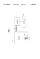
FIG. 1 is a schematic view of a microwave applying apparatus employed in the present invention;
FIG. 2 is a graph showing a temperature change with respect to a thermal processing time for the purpose of observing a suscetpibility of a rapid thermal processing of a material used in an embodiment of the present invention; and
FIG. 3 is an X-ray diffraction (XRD) pattern showing the degree of crystallinity of a PZT thin film resulting from a rapid thermal processing schedule in FIG. 2.
DETAILED DESCRIPTION OF THE PREFERRED EMBODIMENTS
According to the method of using microwaves, among 400 MHz to 40 GHz which is an ISM(Interational Science and Medicine) frequency band allotted for private use, 2.45 GHz is used as a frequency appropriate to the sintering of ceramics, but sometimes 28 GHz and 60 GHz are also used.
The application of microwaves in the fabrication process of ceramics will now be described in detail.
Microwaves are adapted to a processing control in nondestructive inspection, or to a powder synthesis or a sintering by generating a plasma. Furthermore, microwaves make rapid the dissolution speed of a mineral in a solution to be used for the shortening of a wet chemical analysis or to be employed as a thermal source in sintering, bonding and melting ceramics.
The principles of heating a material by using microwaves which have been known so far are as follows:
When microwaves are applied to each different material, the degree of penetration, absorption or reflection occurs differently according to the kind and temperature of the materials. Since microwaves are unable to permeate most metals and are reflected, the metals cannot be heated. On the other hand, microwaves are able to pass through most ceramic dielectric materials (electrical insulating materials) such as Al2 O3, MgO, SiO2 at room temperature, but when the above materials are heated over a critical temperature, they carry out a gradual coupling with microwave energy so that they can absorb it effectively. A conductive or magnetic material such as Co2 O3, MnO2, NiO, Fe2 O3, CuO and a carbon black begins to absorb microwaves at a room temperature. When these materials absorbing microwaves are added to microwave-penetrable ceramic materials in the shape of a fiber or a particle, a selective heating occurs such that they react with microwaves faster than in a matrix, resulting in increasing the effect that the whole material absorbs the microwave energy.
The phenomenon that when microwave energy is applied to a material the material is heated thereby can be explained by dielectric loss resulting from a polarization. The polarization agents of the material include an electronic, atomic or ionic, dipole or orientation, and a space charge polarization.
Which polarization agent can effectively function depends on the kind of material and the frequency and temperature of the electromagnetic waves. In the microwave frequency range, an electronic polarization can mainly function in a macromolecular material, and the space charge polarization occurs at a relatively low frequency and at a boundary region with other materials. An exothermic phenomenon occurring within a frequency range of 10 GHz is caused by the atomic and dipole polarizations, among which the dipole polarization is a main agent for the exothermic phenomenon.
When an electrical field is applied to a ceramic dielectric body in which dipoles are disorderly arranged, the dipoles in the electric field tend to be oriented in the opposite direction of the electric field. When the dipoles are oriented in such a direction, since an electric field is generated by the dipoles in the opposite direction to the external electric field, an internal electric field is reduced. But, when a rapidly changing electric field occurring at a frequency of 1 GHz corresponding to a microwave region is applied to the ceramic, a dipole which is a physical entity with a mass and an inertia can not catch up with the changing speed of an electric field, and as a result, potential energy is accumulated. The potential energy is converted into a random kinetic energy, which is emitted in the form of heat to the ceramics.
As described above, the absorption and permeation of microwaves in a material depend on a dielectric characteristic of the material. Therefore, to understand and predict an exothermic characteristic of a material by microwaves, the dielectric characteristics of the material and the factor causing the characteristic must be understood. In a process of heating with microwaves, the rate of temperature elevation is determined by the temperature, an effective loss factor and a field strength.
Generally, while the ceramic is heated by microwaves from a room temperature to a sintering temperature, its thermal capacity and density are doubled, but the loss factor is increased up to over 10 times. Therefore, to control the loss factor of a heated material is the most important thing in a thermal process using microwaves. And, since the thermal loss is rapidly increased by radiation at a high temperature region in which a sintering is performed, an adiabatic construction is also required.
When a material reaches a critical temperature while being heated using microwaves, tan ∂ (dielectric loss) is rapidly increased, and the temperature is also rapidly elevated. When the tan ∂ is rapidly increased, the material absorbs microwave energy more effectively, resulting in elevating its temperature. Then, the temperature elevation increases tan a much faster again.
By a series of accelerating effects, a exponential increase of the temperature is caused, which is called a thermal runaway. The temperature at which the thermal runaway develops is dependent upon each material. Description of the thermal runaway condition on which the exponential increase of the temperature arises will be given, taking two kinds of materials, for example.
Since an A-type material has a low tan ∂ at a normal temperature, the thermal runaway does not develop in an output range applied to a B-type material, but when an output is elevated sufficiently, an absorption efficiency is increased accordingly, resulting in the development of the thermal runaway. The B-type material absorbs microwaves at room temperature effectively, and the application of a predetermined output of microwave energy to a sample causes the thermal runaway to occur rapidly. The initial heated shape of Cr2 O3 is similar to the A-type material, and that of Fe3 O4 to the B-type material.
The thermal runaway plays an important role in heating by microwaves. The basic reason is a rapid temperature elevation, and when a material is not uniform, the generation of an undesirable hot spot and melting in a local section causes a thermal shock, resulting in the destruction of the material. Therefore, special care is required in sintering ceramics.
FIG. 1 is a schematic view of a microwave applying apparatus employed in the present invention which includes a generator 7 for generating microwave an applicator 1 used as a chamber for interacting a material and microwave, a waveguide section 6 for transmitting and adjusting the generated microwave by connecting the generator 7 and the applicator 1 and a control unit 8 for controlling the generation of the microwave energy.
The microwave applying apparatus employs a multimode applying method, wherein the simple structure and the easy manufacture advantageously enable the apparatus to not be influenced by the size of the material to be applied. However, when the number of modes created in the applicator is small even though it is composed of multimode, the distribution of the electric field is disadvantageously rendered irregular. To solve this defect, the parts having a different size of an electric field are allowed to pass at a constant speed by using a rotary platen, or several modes are allowed to be created simultaneously by stirring an electric field of the portion to which microwaves are incident in the applicator by an irregular reflection with a propeller-shaped mode agitator.
A fused quartz which the microwave is transmitted and can safely endure at a high temperature is used as a support 4, and thereon, a silicon substrate is placed as a substrate support 3 as in a rapid heating apparatus using a general radiation heating and a substrate 2 deposited with the ceramic thin film is placed on the substrate support 3. When a rapid thermal processing is carried out on a large size wafer having a diameter of over 1 to 2 inches, the self rapid thermal processing can be performed without the need of a silicon substrate support.
When the substrate support 3 is used, the temperature can be measured by etching the back surface of silicon wafer, by inserting a small thermocouple tip(a bead-shaped tip) 5 therein, and fixing the same with a conductive adherent(for example, Ag paste etc.). Then a shielding is performed on the surface of the thermocouple line to prevent its reaction with microwave energy.
Another method of measuring the temperature is to stack two sheets of silicon wafers on the support, to minimize the space between the stacked wafers to be smaller than the wavelength of the microwaves, to insert a thermocouple bead therebetween and then fix the same with a conductive adherent. Here, a shielding is also performed on the surface of the thermocouple line to prevent its reaction with microwaves.
Still another method of measuring the temperature is to sense a wafer temperature by a non-contact method, using an optical fiber-type small pyrometer. Here, since the optical fiber itself is composed of quratz and does not react with microwaves, it can be easily fused.
When processing a large sized wafer, which obviates the necessity of a silicon substrate support, that is, when there is no substrate support on which a thermocouple can be disposed, a wafer for measuring a temperature on which a thermocouple is affixed must be provided or a pyrometer must be equipped. When the optical fiber pyrometer is used to read the temperature, since the film for undergoing a thermal processing is deposited on the front surface of the wafer, the pyrometer must be disposed to read the back surface of the wafer.
When a thin film is coated in which a thermal runaway does not develop or the development degree is not satisfactory although the material is exposed to microwaves in a thermal processing, a rapid heating using microwaves is difficult to carry out. Therefore, if a material in which a thermal runaway easily develops is used as a substrate on which a thin film is to be coated, it must be selected to allow a rapid heating of the substrate to be easily rendered, resulting in achieving the effect of the thermal processing of the coated thin film thereon.
FIG. 2 is a graph showing a temperature change with respect to time in a thermal processing for the purpose of observing a susceptibility for a rapid thermal processing of a material used in an embodiment of the present invention.
The materials used in the experiment were a bare silicon wafer and a Pb(Zr0.52 Ti0.48)O3 thin film having a thickness of 4000 Å deposited on a Pt/Ti/SiO2 /Si(100) substrate at a substrate temperature of 420° C. by a sputtering method. In the case of a bare silicon substrate, when about forty seconds passes after microwave energy is applied, the temperature reaches a peak within 5 minutes, and in the case of the substrate on which a PZT thin film is deposited, the temperature starts to increase after twenty seconds, and reaches a point to be thermally processed within about five seconds.
As mentioned above, in case a rapid thermal processing is carried using microwaves, a temperature increase rate of about 120° C. per second can be obtained, and the increasing rate can be controlled in accordance with the applied power to the microwave oven. The above-described rapid increase of the temperature shows a susceptibility or amenability for a rapid thermal processing.
FIG. 3 is an XRD pattern showing the degree of crystallinity of a PZT thin film resulting from the rapid thermal processing schedule in FIG. 2.
The XRD patterns are those of an As-deposited thin film at 420° C., of a thin film of which a thermal processing was performed at 500° to 700° C. and of a thin film of which a thermal processing was performed at 680° C. by microwaves. When comparing the patterns with each other, the thermal processing at 680° C. by microwaves has a better effect than any other processing. In the processing at 680° C., a rapid increase of PZTs (100)(200) peak can be observed, and the increasing width is incomparably large in comparison with the case of the processing at 700° C. Therefore, the crystallinity of the deposited thin film has been increased by the rapid thermal processing using microwaves according to the present invention.
Although the preferred embodiments of the present invention have been disclosed for illustrative purposes, those skilled in the art will appreciate that various modifications, additions and substitutions are possible, without departing from the scope and spirit of the invention as recited in the accompanying claims.

Claims (8)

What is claimed is:
1. A rapid thermal processing method for a ferroelectric, high dielectric, electrotrictive, semiconductive, or conductive ceramic thin film using microwaves, which method comprising:
disposing a material deposited with the ceramic thin film on a first supporting means;
applying microwaves uniformly on the material and heating the material deposited with the ceramic thin film rapidly;
measuring a temperature of the material by using a temperature measuring means; and
halting the generation of the microwaves when the temperature of the material reaches a desired temperature.
2. The method of claim 1, comprising:
disposing a second support means for the material on the first supporting means and placing the material on the second supporting means.
3. The method of claim 2, comprising:
etching a back surface of the second supporting means; and
inserting a thermocouple as the temperature measuring means therein to measure the temperature.
4. The method of claim 3, wherein the thermocouple has a shielded thermocouple line.
5. The method of claim 2, comprising:
stacking the second supporting means no less than two folds; and
inserting a thermocouple as the temperature measuring means between the folded second supporting means to measure the temperature.
6. The method of claim 5, wherein the thermocouple has a shielded thermocouple line.
7. The method of claim 1, wherein the temperature measuring means is a pyrometer.
8. The method of claim 1, wherein the heating is carried out under a thermal insulation condition by surrounding the material with insulation materials.
US08/757,859 1996-07-16 1996-11-27 Rapid thermal processing method for ferroelectric, high dielectric, electrostrictive, semiconductive, or conductive ceramic thin film using microwaves Expired - Fee Related US5796079A (en)

Applications Claiming Priority (2)

Application Number Priority Date Filing Date Title
KR28713/1996 1996-07-16
KR1019960028713A KR100197157B1 (en) 1996-07-16 1996-07-16 Rapid thermal processing method for ferroelectric, high dielectric, electrostrictive, semiconductive, or conductive ceramic thin film using microwaves

Publications (1)

Publication Number Publication Date
US5796079A true US5796079A (en) 1998-08-18

Family

ID=19466488

Family Applications (1)

Application Number Title Priority Date Filing Date
US08/757,859 Expired - Fee Related US5796079A (en) 1996-07-16 1996-11-27 Rapid thermal processing method for ferroelectric, high dielectric, electrostrictive, semiconductive, or conductive ceramic thin film using microwaves

Country Status (2)

Country Link
US (1) US5796079A (en)
KR (1) KR100197157B1 (en)

Cited By (11)

* Cited by examiner, † Cited by third party
Publication number Priority date Publication date Assignee Title
US6365885B1 (en) 1999-10-18 2002-04-02 The Penn State Research Foundation Microwave processing in pure H fields and pure E fields
US6384390B1 (en) 1997-12-31 2002-05-07 Samsung Electronics Co., Ltd. Apparatus for forming thin film using microwave and method therefor
US20040159335A1 (en) * 2002-05-17 2004-08-19 P.C.T. Systems, Inc. Method and apparatus for removing organic layers
US20060009021A1 (en) * 2004-07-06 2006-01-12 Herman Gregory S Structure formation
US20060258040A1 (en) * 2005-05-11 2006-11-16 Instrument Technology Research Center, National Applied Research Laboratories Microsensor with ferroelectric material and method for fabricating the same
US20070215607A1 (en) * 2006-03-20 2007-09-20 Wander Joseph M Apparatus and method for heating semiconductor wafers via microwares
US20100215869A1 (en) * 2007-06-27 2010-08-26 Siemens Aktiengesellschaft Method for generating a ceramic layer on a component
US20110226759A1 (en) * 2007-03-08 2011-09-22 Wander Joseph M Apparatus and method for heating semiconductor wafers via microwaves
US20130153813A1 (en) * 2010-07-27 2013-06-20 Youtec Co. Ltd. Poling treatment method, plasma poling device, piezoelectric substance, and manfacturing method therefor
US11741428B1 (en) 2022-12-23 2023-08-29 Kepler Computing Inc. Iterative monetization of process development of non-linear polar material and devices
US11769790B2 (en) 2022-01-31 2023-09-26 Kepler Computing Inc. Rapid thermal annealing (RTA) methodologies for integration of perovskite-material based trench capacitors

Families Citing this family (1)

* Cited by examiner, † Cited by third party
Publication number Priority date Publication date Assignee Title
KR100482653B1 (en) * 2002-06-03 2005-04-13 한국화학연구원 Process for preparing nano-fabrication of inorganic thin films by microwave irradiation

Citations (7)

* Cited by examiner, † Cited by third party
Publication number Priority date Publication date Assignee Title
US4622447A (en) * 1982-04-09 1986-11-11 Fujitsu Limited Microwave apparatus for vacuum treating and heating a semiconductor substrate
US4683363A (en) * 1981-09-17 1987-07-28 Itt Industries Inc. Microwave apparatus for processing semiconductor
US4963709A (en) * 1987-07-24 1990-10-16 The United States Of America As Represented By The Department Of Energy Method and device for microwave sintering large ceramic articles
US5036172A (en) * 1988-09-23 1991-07-30 Whirlpool International B.V. Method and device for determining when a food has thawed in a microwave oven
US5124179A (en) * 1990-09-13 1992-06-23 Diamonex, Incorporated Interrupted method for producing multilayered polycrystalline diamond films
US5417494A (en) * 1992-05-01 1995-05-23 Exid, Inc. Contactless testing of electronic materials and devices using microwaves
US5459302A (en) * 1991-12-23 1995-10-17 Societe Prolabo Apparatus and process for measuring the temperature of a sample heated in a microwave chamber

Patent Citations (7)

* Cited by examiner, † Cited by third party
Publication number Priority date Publication date Assignee Title
US4683363A (en) * 1981-09-17 1987-07-28 Itt Industries Inc. Microwave apparatus for processing semiconductor
US4622447A (en) * 1982-04-09 1986-11-11 Fujitsu Limited Microwave apparatus for vacuum treating and heating a semiconductor substrate
US4963709A (en) * 1987-07-24 1990-10-16 The United States Of America As Represented By The Department Of Energy Method and device for microwave sintering large ceramic articles
US5036172A (en) * 1988-09-23 1991-07-30 Whirlpool International B.V. Method and device for determining when a food has thawed in a microwave oven
US5124179A (en) * 1990-09-13 1992-06-23 Diamonex, Incorporated Interrupted method for producing multilayered polycrystalline diamond films
US5459302A (en) * 1991-12-23 1995-10-17 Societe Prolabo Apparatus and process for measuring the temperature of a sample heated in a microwave chamber
US5417494A (en) * 1992-05-01 1995-05-23 Exid, Inc. Contactless testing of electronic materials and devices using microwaves

Non-Patent Citations (6)

* Cited by examiner, † Cited by third party
Title
C.V.R. Vasant Kumar, et al., "Crystallization of sputtered lead zirconate titanate films by rapid thermal processing," J. Appl. Phys., 71(2), 15 Jan. 1992, pp. 864-874.
C.V.R. Vasant Kumar, et al., Crystallization of sputtered lead zirconate titanate films by rapid thermal processing, J. Appl. Phys. , 71(2), 15 Jan. 1992, pp. 864 874. *
S. L. Zhang, et al., Rapid thermal processing with microwave heating, Thin Solid Films , 246 (1994) pp. 151 157. *
S.-L. Zhang, et al., "Rapid thermal processing with microwave heating," Thin Solid Films, 246 (1994) pp. 151-157.
Willard H. Sutton, "Microwave Processing of Ceramic Materials," Ceramic Bulletin, vol. 68, No. 2, 1989, pp. 376-386.
Willard H. Sutton, Microwave Processing of Ceramic Materials, Ceramic Bulletin , vol. 68, No. 2, 1989, pp. 376 386. *

Cited By (18)

* Cited by examiner, † Cited by third party
Publication number Priority date Publication date Assignee Title
US6384390B1 (en) 1997-12-31 2002-05-07 Samsung Electronics Co., Ltd. Apparatus for forming thin film using microwave and method therefor
US6365885B1 (en) 1999-10-18 2002-04-02 The Penn State Research Foundation Microwave processing in pure H fields and pure E fields
US20040159335A1 (en) * 2002-05-17 2004-08-19 P.C.T. Systems, Inc. Method and apparatus for removing organic layers
US7547647B2 (en) 2004-07-06 2009-06-16 Hewlett-Packard Development Company, L.P. Method of making a structure
US20060009021A1 (en) * 2004-07-06 2006-01-12 Herman Gregory S Structure formation
US8143616B2 (en) 2004-07-06 2012-03-27 Oregon State University Making a structure
US20090200541A1 (en) * 2004-07-06 2009-08-13 Hewlett-Packard Development Company Lp Making a structure
US20060258040A1 (en) * 2005-05-11 2006-11-16 Instrument Technology Research Center, National Applied Research Laboratories Microsensor with ferroelectric material and method for fabricating the same
US7413912B2 (en) * 2005-05-11 2008-08-19 Instrument Technology Research Center, National Applied Research Laboratories Microsensor with ferroelectric material and method for fabricating the same
US20070215607A1 (en) * 2006-03-20 2007-09-20 Wander Joseph M Apparatus and method for heating semiconductor wafers via microwares
US20110226759A1 (en) * 2007-03-08 2011-09-22 Wander Joseph M Apparatus and method for heating semiconductor wafers via microwaves
US9048270B2 (en) * 2007-03-08 2015-06-02 Joseph M. Wander Apparatus and method for heating semiconductor wafers via microwaves
US20100215869A1 (en) * 2007-06-27 2010-08-26 Siemens Aktiengesellschaft Method for generating a ceramic layer on a component
US20130153813A1 (en) * 2010-07-27 2013-06-20 Youtec Co. Ltd. Poling treatment method, plasma poling device, piezoelectric substance, and manfacturing method therefor
US11769790B2 (en) 2022-01-31 2023-09-26 Kepler Computing Inc. Rapid thermal annealing (RTA) methodologies for integration of perovskite-material based trench capacitors
US11894417B2 (en) 2022-01-31 2024-02-06 Kepler Computing Inc. Method of fabricating a perovskite-material based trench capacitor using rapid thermal annealing (RTA) methodologies
US11908704B2 (en) 2022-01-31 2024-02-20 Kepler Computing Inc. Method of fabricating a perovskite-material based planar capacitor using rapid thermal annealing (RTA) methodologies
US11741428B1 (en) 2022-12-23 2023-08-29 Kepler Computing Inc. Iterative monetization of process development of non-linear polar material and devices

Also Published As

Publication number Publication date
KR100197157B1 (en) 1999-06-15
KR980012100A (en) 1998-04-30

Similar Documents

Publication Publication Date Title
US5796079A (en) Rapid thermal processing method for ferroelectric, high dielectric, electrostrictive, semiconductive, or conductive ceramic thin film using microwaves
Tantigate et al. Processing and properties of Pb (Mg1/3Nb2/3) O3–PbTiO3 thin films by pulsed laser deposition
Yang et al. Schottky barrier effects in the electronic conduction of sol–gel derived lead zirconate titanate thin film capacitors
Cheng Structural and optical properties of laser deposited ferroelectric (Sr0. 2Ba0. 8) TiO3 thin films
Al‐Shareef et al. Low temperature processing of Nb‐doped Pb (Zr, Ti) O3 capacitors with La0. 5Sr0. 5CoO3 electrodes
Pan et al. Low-temperature processing of sol-gel derived La 0.5 Sr 0.5 MnO 3 buffer electrode and PbZr 0.52 Ti 0.48 O 3 films using CO 2 laser annealing
Zhu et al. Amorphous ferroelectric (Ba 0.67 Sr 0.33) Ti 1.02 O 3 thin films with enhanced H 2 induced interfacial polarization potential
Yeh et al. Electrical characteristics of barium titanate films prepared by laser ablation
Yuan et al. Temperature-dependent fatigue behaviors of ferroelectric ABO 3-type and layered perovskite oxide thin films
Son et al. Electrocaloric effect of perovskite high entropy oxide films
Shi et al. Development of ferroelectric Pb (ZrxTi1− x) O3 thin films by metallo-organic decomposition process and rapid thermal annealing
US5143894A (en) Formation and high resolution patterning of superconductors
Chen et al. Lead Zirconate Titanate Films on Nickel–Titanium Shape Memory Alloys: SMARTIES
JP2002280380A (en) Method of forming film for semiconductor device
US6620456B2 (en) Forming a dielectric layer by thermal decomposition of a metallo-organic material
Khodorov et al. Impedance spectroscopy study of a compositionally graded lead zirconate titanate structure
Zhu et al. Raman, FT-IR and dielectric studies of PZT 40/60 films deposited by MOD technology
Ho et al. Characterization of (Pb, La) TiO 3 thin films prepared by the sol-gel method
Taylor et al. Integration Aspects and Electrical Properties of SrBi2Ta2O9 for Non-Volatile Memory Applications
Hadni et al. Review of recent improvements in pyroelectric detectors
Lienhard et al. A matrix formalism for the simulation of pyroelectric sensors
Bauer et al. Design and properties of a microcalorimeter
Ioachim et al. Dielectric properties of (Ba, Sr) TiO3 thin films for applications in electronics
Cho et al. Structure and electrical properties of Pb (Zr, Ti) O3 thin films deposited by reactive sputtering using multi-targets
JP2006190716A (en) Ferroelectric memory element and its manufacturing method

Legal Events

Date Code Title Description
AS Assignment

Owner name: KOREA INSTITUTE OF SCIENCE AND TECHNOLOGY, KOREA,

Free format text: ASSIGNMENT OF ASSIGNORS INTEREST;ASSIGNORS:KIM, TAE SONG;JUNG, HYUNG JIN;KIM, DO KYUNG;AND OTHERS;REEL/FRAME:008348/0169

Effective date: 19961021

FEPP Fee payment procedure

Free format text: PAYOR NUMBER ASSIGNED (ORIGINAL EVENT CODE: ASPN); ENTITY STATUS OF PATENT OWNER: SMALL ENTITY

FPAY Fee payment

Year of fee payment: 4

REMI Maintenance fee reminder mailed
LAPS Lapse for failure to pay maintenance fees
STCH Information on status: patent discontinuation

Free format text: PATENT EXPIRED DUE TO NONPAYMENT OF MAINTENANCE FEES UNDER 37 CFR 1.362

FP Lapsed due to failure to pay maintenance fee

Effective date: 20060818