US5793158A - Gas discharge (plasma) displays - Google Patents
Gas discharge (plasma) displays Download PDFInfo
- Publication number
- US5793158A US5793158A US08/864,896 US86489697A US5793158A US 5793158 A US5793158 A US 5793158A US 86489697 A US86489697 A US 86489697A US 5793158 A US5793158 A US 5793158A
- Authority
- US
- United States
- Prior art keywords
- phosphor
- substrate
- dielectric
- channels
- channel
- Prior art date
- Legal status (The legal status is an assumption and is not a legal conclusion. Google has not performed a legal analysis and makes no representation as to the accuracy of the status listed.)
- Expired - Lifetime
Links
Images


Classifications
-
- H—ELECTRICITY
- H01—ELECTRIC ELEMENTS
- H01J—ELECTRIC DISCHARGE TUBES OR DISCHARGE LAMPS
- H01J11/00—Gas-filled discharge tubes with alternating current induction of the discharge, e.g. alternating current plasma display panels [AC-PDP]; Gas-filled discharge tubes without any main electrode inside the vessel; Gas-filled discharge tubes with at least one main electrode outside the vessel
- H01J11/10—AC-PDPs with at least one main electrode being out of contact with the plasma
- H01J11/12—AC-PDPs with at least one main electrode being out of contact with the plasma with main electrodes provided on both sides of the discharge space
-
- H—ELECTRICITY
- H01—ELECTRIC ELEMENTS
- H01J—ELECTRIC DISCHARGE TUBES OR DISCHARGE LAMPS
- H01J11/00—Gas-filled discharge tubes with alternating current induction of the discharge, e.g. alternating current plasma display panels [AC-PDP]; Gas-filled discharge tubes without any main electrode inside the vessel; Gas-filled discharge tubes with at least one main electrode outside the vessel
- H01J11/20—Constructional details
- H01J11/34—Vessels, containers or parts thereof, e.g. substrates
- H01J11/42—Fluorescent layers
Definitions
- This invention relates to gas discharge (plasma) displays, and more particularly to color gas discharge display panels.
- Multiple cell gas discharge display and/or memory panels of one particular type with which the present invention is concerned are characterized by an ionizable gaseous medium, at an appropriate gas pressure, in a thin gas chamber or space between a pair of opposed dielectric charge storage members.
- the dielectric charge storage members are typically backed by arrays of electrodes or conductors which are appropriately oriented so as to define a plurality of discrete gas discharge unit or cell sites.
- the discharge cells are additionally defined by surrounding or confining physical structures such as apertures in perforated glass plates and the like so as to be physically isolated relative to other cells.
- the dielectric members prevent the passage of substantial conductive current from the conductor members to the gaseous medium and also serve to collect or store ionized gaseous medium charges during the cycles of the operating potentials. Such charges collect first at one elemental or discrete dielectric surface area and then at an opposing elemental or discrete dielectric surface area on alternate half cycles to constitute the electrical memory.
- a monolithic or single substrate device structure may also be used as disclosed in U.S. Pat. Nos. 3,860,846 (Mayer), 3,964,050 (Mayer), 4,080,597 (Mayer), 3,646,384 (Lay) and 3,896,327 (Schermerhorn), all incorporated herein by reference.
- a continuous volume of ionizable gas is confined between a pair of dielectric surfaces backed by electrode arrays typically forming matrix elements locating individual pixels in the display.
- the two electrode arrays may be orthogonally related sets of parallel lines. However, any other configuration of electrodes may be used.
- the two arrays of electrodes define at their crossovers a plurality of opposed pairs of charge storage areas on the opposing surfaces of the dielectric members bonding or confining the gas.
- the number of gas discharge cells will be the multiple of R times C.
- the number of dielectric charge storage locations will be twice the number of discharge cells where the electrodes of each array are separated from the gas by a dielectric member.
- a first dielectric layer is applied over a first array of X-electrodes and a second array of Y-electrodes is applied over the first dielectric layer.
- a second dielectric layer is then applied over the second array of Y-electrodes.
- a top envelope portion is applied over the substrate and filled with ionizable gas such that a chamber of gas is above the second dielectric layer.
- the dielectric applied over the bottom X-electrodes must be capable of physically, mechanically and structurally supporting the array of top Y-electrodes applied over the first dielectric portion without flexure or movement of the electrodes.
- Such dielectric support of the Y-electrodes is especially important during the various process thermal cycles.
- it is important that the supporting dielectric portion not become soft and flow or develop cracks or flaws during the application of the Y-electrode or during the application of a second dielectric portion covering the Y-electrodes or during the sealing together of the envelope and substrate.
- alternating current plasma display panel in which an etched or chemically milled imperforate barrier structure has upstanding posts with cell sidewalls defining concavities intermediate the posts.
- the imperforate structure has a plurality of such concavities, each associated with a unique cell and providing an intercell barrier structure.
- the cell sidewalls are provided with priming particle passing gaps and UV responsive phosphor islands are deposited on the surface of a front dielectric structure.
- elongated channels, troughs or grooves are chemically milled in the dielectric layers, and the channels, troughs, or grooves have elongated ribs or lands therebetween.
- the sloping rib walls are coated with a phosphor structure (undercoat/phosphor/overcoat) which significantly enhances the light output because the phosphor surfaces are greater in extent area-wise, closer to the UV sources in the discharge and are not in the path of discharge products. Since light is produced in two spaced areas of phosphor by the UV produced on discharge, more light is produced and the electrodes have less attenuating effect on visible light emission from each side.
- the seal area or zone (for securing a second electrode bearing substrate to form the matrix) can be on the first dielectric layer with the ends of the channels, troughs or grooves formed in the second (and even third) dielectric layer being in free connection via a transition corridor for exemplary or ideal vacuum bake-out operations with the transition corridor serving as the site for border conditioning discharge sites.
- the manufacturing process comprises:
- the dielectric face of the second substrate over the dielectric grooves, channels or troughs of the first substrate, the array of electrodes on the second substrate being appropriately oriented relative to the array of electrodes on the first substrate so as to define a plurality of discrete gas discharge units or cell sites;
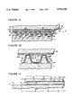
- FIG. 1A is an isometric perspective view of an AC plasma color display panel incorporating the invention with various layers and components removed to reveal the physical construction
- FIG. 1B is a greatly enlarged diagrammatic sectional view through one discharge site of an AC plasma color display panel incorporating the invention
- FIG. 1C is a greatly enlarged diagrammatic view through the seal/transition corridor area of the panel shown in FIGS. 1A and 1B,
- FIG. 1D is a block diagram of a color gas discharge system incorporating the invention including multi-media interfacing, gray scale and a color AC plasma display panel.
- FIG. 2 is a flow diagram for the etching process for forming dielectric channels and barriers. This is discussed hereinafter as part of a working example.
- FIG. 3 is a representation ETCHANT CHARACTERIZATION CURVE
- FIG. 4 is a flow diagram for the PHOSPHOR APPLICATION PROCESS. This is discussed hereinafter as part of a working example.
- a display panel 10 incorporating the invention has a first substrate 11, typically a glass or ceramic substrate, has a first electrode array 12-1, 12-2, 12-3 . . . 12-N formed thereon.
- electrode arrays are preferably gold on a tantalum base.
- alternate electrodes extend to the opposite edge of the substrate.
- Electrode array 12-1, 12-2 . . . 12-N is coated with dielectric layers to form two regions, a seal transition corridor or region SC best seen in FIG. 1C and a display region DR.
- the seal region or corridor SC is not shown in the illustration.
- the seal transition corridor or region SC has a thin dielectric coating 19 on electrode array 12-1, 12-2 . . . 12-N.
- Viewing side substrate 20 is transparent and carries electrode array 21-1, 21-2 . . . 21-N and a thin dielectric coating 22 which is uniformly applied thereover and both dielectric coatings 19 and 22 can have one or more protective overcoats applied as will be described hereafter.
- a glass seal frame member 24 is fusibly sealed to the surfaces of dielectric coatings or layers 19 and 22 to form a vacuum backable hermetic enclosure.
- the dielectric on substrate 11 which is in the display region DR has formed therein an array of discharge gas filled grooves, channels or troughs 25 separated by ribs or lands 26.
- the dielectric in the display region DR is preferably applied in several layers or applications, so as to achieve uniformity and thickness sufficient to form the array of grooves, channel or troughs 25 separated by ribs or land 26.
- One or more of the dielectric layers may include a black colorant so that the later applied phosphor strips or dots have a black background or surround.
- the grooves, channels or troughs 25 are formed by chemical milling processes described later herein.
- the edge of the display region (e.g., where the grooves, channels or troughs 25 and ribs 26 end or terminate, is spaced from the inside edge of seal member 24 a short distance). This allows the vacuum bake out and discharge gas filling, through gas fill tubulation 28, to take place in all of the grooves, channels or troughs 25 uniformly.
- one or more columns or rows of border discharge sites between one or more border electrodes 27 and the electrodes in electrode array 12-1, 12-2 . . . 12-N for conditioning purposes can be provided in this area and, preferably, masked from view. It is common practice to provide such border discharge sites to provide conditioning of discharge sites in the display region DR for discharge at more uniform operating potentials.
- transition or seal corridor serves three basic functions: seal area, vacuum bake-out and discharge gas fill corridor and for conditioning purposes to assure more uniform operating potentials at each discharge site.
- conditioning can be provided by edge discharges in the grooves, channels or troughs 25 and such conditioning discharge sites likewise masked from view.
- FIGS. 1A and 1B The construction of display region DR is best seen in FIGS. 1A and 1B.
- undercoat 30 is applied in one or more continuous layers.
- Undercoat 30 provides a protective base for UV responsive phosphors (photoluminescent) on the two sidewalls of the barrier ribs or lands 26 forming each channel or groove 25.
- UV responsive phosphors photoluminescent
- each channel or groove will have two curved walls facing each other carrying Uw responsive phosphor of a selected color emissivity.
- the two opposed wall surfaces 26WL and 26WR or ribs or barriers 26 would have blue phosphor stripes 32L and 32R applied over the continuous undercoat layer 30.
- Surfaces in the discharge spaces or volume V between electrode 12N and the opposing electrodes on viewing substrate 20 are preferably free of phosphor so as to not interfere with the discharge or memory characteristics of the discharge site. From the viewing side, the light emitted by phosphor on the two sloping sidewalls is additive and tend to provide a brighter color display.
- the particles of phosphor on the sloping surfaces can be thought of as individual sources which, due to the slope, have a stacked vertical component of light produced.
- surfaces of phosphor layers 32L and 32R face upwards and are on the optical isolation barriers constituted by ribs or barriers 26 and the walls 26WL and 26WR are at an angle to the plane of the substrate except at the bottom of the channel or groove.
- the slope ( ⁇ ) of the rib wall should not affect the discharge itself. The slope will determine total surface area available for phosphor deposition, i.e., more curved, more surface area for deposition of phosphor. The more phosphor particles, more surface area of phosphor particles is available for UV conversion, and hence, a higher efficiency of UV conversion.
- a sloped wall gives a slightly better viewing angle but the main point is the discharge gap. A smaller gap results in a better viewing angle. Since smaller gap is for higher resolution displays, a higher resolution provides a better viewing angle.
- the two phosphor stripes are simultaneously activated by the UV emission during any discharge and while there are two sources of visible light production (one from each phosphor) and because the spacing between the two phosphor stripes is small, and because light is also reflected off of the reflective mirror-like surface of the gold electrode 12N, the luminous efficiency is enhanced.
- the surfaces of the phosphor impinged by UV is caused to emit light and that surface is viewed directly through the viewing substrate. This is in contrast to those systems where the phosphor is on the viewing substrate so that light travels through the phosphor.
- each individual cross-point defines a color pixel (blue, green or red) which can be selectively controlled to produce a large number of levels of gray intensity levels, (e.g., brightness levels ranging from a maximum to a minimum) and, accordingly, a large palette of colors by different permutations of these colors and color intensity level.
- gray intensity levels e.g., brightness levels ranging from a maximum to a minimum
- palette of colors by different permutations of these colors and color intensity level.
- there is no optical cross-talk between adjacent sites because of the barriers 26.
- There is no optical isolation between adjacent sites along each channel because they are of the same color and cross-talk effects, if any, can be minimized by optionally providing a somewhat larger spacing between electrodes 21-1, 21-2 . . . 21-N.
- the facing surfaces 26WL and 26WR of the ribs carrying phosphor layers or stripes 32L and 32R are sloped and at an angle ⁇ relative to the substrate 11. It is desirable to provide a flat valley in groove, trough or channel 25, over the electrode aligned with groove, trough or channel.
- the chemical milling process described later herein can be controlled to generally control the angle ⁇ and provide a substantially flat dielectric valley over the electrodes.
- the three photoluminescent phosphors are applied in stages for a full color embodiment, a separate stage for each phosphor.
- a single application of premixed red, green and blue phosphors in the right proportions would occur.
- a continuous protective overcoat 40 is applied over the entire surface of the phosphor stripes 32L, 32R and the undercoat 30.
- the overcoat 40 protects the dielectric surfaces over the electrodes from deterioration due to ion bombardment, sputtering, etc., and also is of a material which has excellent secondary electron emissivity for conditioning purposes.
- the phosphor layers are protectively sandwiched between the continuous undercoat layer 30 and the continuous overcoat layer 40 and, since the phosphors are not in line with the path of electron and ion travel from discharge between the rear and front electrodes, there is substantially no deterioration in the phosphors leading to long life and constant phosphor efficiency and constant light output.
- the overcoat layers are relatively very thin, they are essentially transparent to most of the UV radiation which is to be converted to visible light by the UV responsive phosphors, and at the same time, since the overcoat is of a material which is a good secondary electron emitter, the individual sites are conditioned for operation at more uniform operating potentials.
- the discharge gas medium discussed below is selected to be rich in deep UV emission, inter alia, and preferably, does not produce visible light so as to interfere with the visible light output of the phosphor. Since the phosphor bearing sidewalls 26WL and 26WR are relatively near the source of UV in volumetric space V, the UV has to travel a relatively short distance from the point where the UV is created to the point of impact on the phosphors at each side of the discharge volume V.
- the combination of the double phosphor stripes for each discharge site, the nearness of the phosphor to the source of UV (and yet outside the area of phosphor deterioration due to ion bombardment), the protective undercoat and protective overcoat stabilizing and maintaining the phosphor, the mirror-reflective gold electrode and the additive slope angle ⁇ of walls 26WL and 26WR bearing the phosphor provide bright colors with high intensity, stable operations and long display life.
- the viewing side of display panel 10 includes transparent support substrate 20, electrode array 21-1, 21-2 . . . 21-N, covered by a dielectric layer 22, which has one or more protective continuous overcoats 45.
- Border electrodes 27 are positioned in the area of the edge extension EE, which overlies a portion of the transition corridor SC. While the dielectric thicknesses (including overcoats) and discharge gap between border electrodes 27 and the ends of electrodes in array 12-1, 12-2 . . . 12-N are essentially the same, so that write, erase and sustain potentials are essentially the same, in some cases it may be desirable that they be different. This can be achieved by selectively varying the dielectric thickness in the border discharge site area.
- FIG. 1D is a block diagram of AC plasma display systems wherein one of a variety of video data sources such as television 50TV, tape recorder 50VCR, video camera 50C, computer 50SVGA, etc. is coupled by interface system 51 to a gray scale processing system 52 and thence to AC plasma color display panel 10' which can be constructed in a high definition television (HDTV) format.
- video data sources such as television 50TV, tape recorder 50VCR, video camera 50C, computer 50SVGA, etc.
- HDTV high definition television
- Digitized video from a video source 50 (above the dashline) is presented to the drive system 51 (below the dashline) as a byte serial stream of pixel data on data bus 55.
- a byte is defined as 6 to 8 bits which represent at least 64 levels of gray scale for each pixel within each color channel.
- FIG. 1D is shown the functional diagram of the drive system 51 along with the functional diagram of the video source and interface system 50.
- the architecture of drive system 51 will accept 7 and 8 bit bytes for 128 and 256 levels of gray for each pixel where faster gas (non-neon) plasma panels are used, particularly those gases which are rich in UV production.
- the video source system 50 may contain a computer 50SVGK with VGA or SVGA or similar type of digitized video output capability.
- the video source may also contain a camera 50TV, VCR 50VCR or TV receiver 50TV, or could also contain a combination of the above.
- the video source and interface system will employ a digitizer which provides the pixel byte stream into drive system 51.
- the digitizer comprises baseband processor 52 and analog-to-digital converter 53 (ADC).
- ADC analog-to-digital converter
- the video source system 50 may also incorporate rescan conversion and/or image processing circuit 54 to adjust gray scale values for global brightness offsets, for dithering techniques, or for non-linear gray scales.
- the digitizer and/or rescan converter may also include "window" portion necessary to show on smaller screens, etc.
- the digitizer and rescan converter can contain circuitry, including memory to selectively capture and resynchronize video images and/or video graphics.
- the baseband processor could also incorporate multisynchronizing capabilities such as exist on many available SVGA-type of monitors today.
- the digitizer and rescan converter could allow the capability, for example, to capture a 512 ⁇ 512 or 480 ⁇ 640 portion from a 768 ⁇ 1024 or HDTV format for the overall image.
- the selected image may then be resynchronized and transferred into the invention's drive system for display. It is also possible that a smaller physical image could be captured and resynchronized; and then displayed by the invention in a selected portion of a bigger matrix image.
- the front end FIFOs 60 contribute to the averaging or smoothing of data rate in synchronization with the digitizer 53. This smoothing of the incoming data rate together with capturing a selected portion of image frames is further discussed below in connection with the operation of the FIFOs and VRAMs.
- the digitizer 53 is a necessary part of an overall display system in which the invention's drive system 51 is employed. In addition to providing the pixel byte stream, the digitizer 52, 53 must provide horizontal and vertical sync 57, and pixel clock 58.
- the invention provides for a timing scheme which allows even and odd frames to be discerned and appropriately processed according to the logic state of horizontal sync at the time of vertical sync deactivation.
- the total number of available colors which can be emitted by a gas discharge display is determined by the number of primary colors and the number of levels or bits of gray scale. For example, with three primary colors (red, green, blue) and two levels (one bit) or gray scale, the number of possible colors is 2 ⁇ 2 ⁇ 2, or 8. For three primary colors and 64 levels (6 bits or 2 6 ), the number of colors is 64 for each primary color or 64 ⁇ 64 ⁇ 64 for three primary colors, a total of 262,144 colors.
- Gray scale may also be accomplished by the operation of an AC plasma panel in a non-memory or non-bistable mode as disclosed in Nolan U.S. Pat. No. 4,002,828 and Ryan U.S. Pat. No. 4,067,047.
- Gray scale may also be accomplished by the technique disclosed in Fowler et al. U.S. Pat. No. 4,006,298.
- the color display uses a gray scale with time modulation.
- FIG. 1D illustrates the functional and schematic diagram for the high density memory architecture in the drive system 51.
- FIFOs 58 Directly receiving the pixel byte stream are FIFOs 58 which accept the bytes on the input and convert the pixel bytes into serial bits at the FIFO outputs 59.
- the serial bit outputs from the FIFOs are tied to the serial inputs of VRAMs 61 as shown in FIG. 1D.
- the high density memory architecture is centered on the serial throughput of pixel data from FIFOs 58 to the inputs of VRAM 60.
- the VRAMs 60 are normally used to accept data in parallel and then output the data to video conversion circuits in serial.
- the parallel inputs to the VRAMs are not fast enough.
- An architecture with SRAMs could be used to allow fast parallel accessing of pixel data through RAM, but significant dual porting control and multiplexing would be required as additional architecture functions; and SRAMs have only about 25% to 50% of the memory density of VRAMs, as well as a higher cost per bit.
- the VRAMs are utilized in the preferred embodiment.
- a typical VRAM circuitry is disclosed in Toshiba Technical Data, TC 528126/AP/AJ-2, 1986-6-1, incorporated herein by reference.
- Separate I/O ports are provided for parallel and serial accessing of the VRAMs interval cell arrays.
- the parallel accessing occurs through combined row/column addressing while the serial accessing occurs through a starting column address and serial address counter.
- the serial address counter operates independently from the addressing except when preset with a starting column address.
- the serial I/O port stores transfer information in a serial access memory (SAM) which buffers column accesses to/from the internal cell array.
- SAM serial access memory
- the VRAMs have built-in dual porting control and multiplexing by shifting into the VRAMs shift register and uploading to the RAM, instead of parallel accessing the VRAM and downloading into their shifting registers (and subsequently into the driver shift registers) pixel data is moved through the VRAM buffer sufficiently fast for the preset invention's requirements.
- Pixel data bus 55, pixel clock on clock bus 56, and horizontal sync and vertical sync on sync bus 57 are supplied to the display drive system 51 to AC plasma panel 10 via the high density memory architecture centered on the serial throughput of pixel data from FIFOs 58 to the VRAMs 61, thence via column driver bus 62 to the column driver 69, and column (X) conductors or electrodes 12 on the AC plasma panel 10.
- Interface controller 65 is a programmed logic device (PLD). Controller 65 receives the pixel clock data and horizontal sync and vertical sync signals on line 66 and issues FIFO control signals on line 67. Interface controller 65 also supplies signals to column or X pulse circuit 68 which supplies the column driver 69.
- interface controller 65 is programmed to control panel drive and row scan controller 70 via lines 71 and line 72.
- Panel drive and row scan controller 70 via bus 73 causes sustainer and row or Y-pulser 74 to issue sustainer drive signals 75 and pulse drive signals on line 76 to row driver circuits 77 which are coupled to the row conductors or electrodes 78 on AC plasma panel 10.
- each display site has an "on” state characterized by the presence of wall voltage on the dielectric surfaces at electrode crossings, and an "off” state characterized by the absence of wall voltage.
- the gray scale drive system shown in FIG. 1D is controlled to supply write, erase, and sustaining potentials to the electrode arrays, in what can be called burst addressing, as follows: 1) the write potential is supplied to all the electrodes to cause all display sites or pixels to be in an "on” state, 2) the erase potential is applied to selected ones of the electrodes in the arrays to erase selected ones of the display sites or pixels and cause the selected ones to be in an "off” state, and finally, 3) a burst of sustaining potentials is supplied to the electrode arrays for predetermined number of cycles to cause the display sites or pixels in the "on” state to emit light for each sustainer cycle.
- Operations 1, 2 and 3 are repeated a predetermined number of times to define a frame and varying the number of sustain cycles in each succeeding repetition of operation 3 for each frame according to the gray scale level desired for each display sites or pixels in the "on" state.
- Burst addressing for gray scale purposes provides the following advantages: 1) artifact reduction, 2) non-linear gray levels, 3) better energy recovery, 4) global dimming, and 5) because of faster scanning, the display is brighter.
- FIG. 3 ETCHANT CHARACTERIZATION CURVE consists of two curves. One is the pedestal for the barriers or walls after the lapse of a given etch time. The other is the etch depth for the channels after the lapse of a given etch time.
- the FIG. 3 is based on the following data:
- the substrate plates 10 and 20 are of a soda lime silica glass composition typically comprising about 73 percent by weight silica, about 14 percent by weight soda, and about 13 percent by weight calcia.
- the working surface of the plate i.e., the surface on which the electrodes and dielectric are deposited, should be flat and free of defects such as scratches, chips, or other blemishes.
- the substrate is of a ceramic or ceramic-like material containing one or more oxides such as aluminum oxide, silicon oxide, titanium oxide, zirconium oxide, magnesium oxide, lead oxide, and so forth.
- the glass substrate is cleaned prior to use.
- cleaning may include chemical treatment such as degreasing with selected solvents.
- Any cleaning process may also include scrubbing with a detergent, rinsing with deionized (DI) water, and drying.
- DI deionized
- Another substrate cleaning process comprises ionic bombardment in a wet active gas as disclosed by U.S. Pat. No. 3,868,271.
- Another substrate cleaning process comprises ultrasonic cleaning where the substrate is emersed in a suitable liquid medium such as degreasing solvents, DI water with or without detergent, or other liquids and subjected to ultrasonic waves.
- a glass substrate may be found to have expanded or contracted. This movement of the glass is especially noticeable after high temperature heating and cooling cycles such as in the firing and curing of the thick film base dielectric and during the burn-out of organic vehicles and solvents from the dielectric and/or phosphor. This movement of the glass may cause alignment problems with artwork or masks, particularly during the various multiple photolithography processes. This glass movement may be uniform or non-uniform and may interfere with the accurate formation and registration of the barriers and phosphor geometry relative to the electrodes. Glass movement, whether uniform or non-uniform, may cause the electrode pitch to change. Further, delamination or stress cracks may occur between subsequent dielectric layerings.
- the movement of the glass substrate through expansion and contraction can be reduced and minimized by preheating the glass substrate to above its annealing temperature and slowly cooling.
- the annealing temperature is above 1000 degrees F.
- the glass substrate is maintained at its annealing temperature for a period of time sufficient to relieve stresses. Typically, this period of time is at least 15 minutes and may be several hours. In the extreme, the glass could be held at or above its annealing temperature for hundreds of hours or more.
- the glass is cooled at a slow rate in order to minimize or prevent the build-up of stresses.
- this cooling rate is about -0.5 deg F. to -2 deg F. per minute.
- This preheating and slow cooling of the glass is typically done before the deposition of the electrodes.
- the end result of this preheating and slow cooling is to relieve stresses and stabilize the glass such that movement of the glass through expansion and contraction during subsequent heating and cooling cycles is greatly reduced. It is believed that the preheating and slow cooling shrinks or compacts the glass and increases its density. Multiple cycles, i.e. at least two or more, of preheating and slow cooling may be used.
- the electrodes or conductors in arrays 12 and 21 may be applied by any suitable means including thick film and/or thin film techniques.
- Typical thick film techniques include screen printing through a stencil or screen.
- Typical thin film techniques include sputtering, resistive heating, electron beam deposition, and chemical vapor deposition.
- the arrays of electrodes or conductors 12 and 21 may be applied to the substrate in any selected pattern.
- the electrode patten is an array of parallel metal conductors.
- These electrodes, at least on the viewing side substrate, may be split or divided with windows or openings such as disclosed in U.S. Pat. No. 3,701,184 to Grier.
- the electrodes may be constructed out of any suitable electrically conductive material such as a pure metal, metal alloy or metal compound of silver, gold, platinum, aluminum, magnesium, zinc, titanium, tantalum, indium, zirconium, nickel, tin, tungsten, chromium, copper, hafnium, gallium, cadmium, niobium, ruthenium, and so forth. Laminates of pure metals and alloys may also be used.
- Specific alloys include gold-platinum, gold-aluminum, gold-silver, copper-silver, copper-chromium, and so forth.
- the electrodes are a chromium-copper-chromium laminate applied to the substrate by a thin film process of the types described above. Reference is also made to U.S Pat. No. 3,837,724.
- the electrodes are of near pure gold. Since gold does not readily adhere to soda lime glass, a thin layer of tantalum or other substance may first be applied to the glass substrate in order to provide an adhering interface for the gold.
- the electrodes are of 99.99% by weight gold deposited to a depth or thickness of about 5,000 to about 25,000 angstrom units over a layer of tantalum deposited on the substrate to a depth or thickness of about 100 to about 500 angstrom units.
- 10,000 angstrom units equal one (1) micron.
- One (1) mil is 0.001 inch and equals 25.4 microns or 254,000 angstrom units.
- the electrodes are of a transparent material such as indium-tin oxide.
- the transparent electrodes may also carry or contain a highly electrically conductive metal or alloy such as gold, nickel, or chrome-copper-chrome.
- This electrically conductive material may serve as an auxiliary electrode to increase or maintain electrical conductivity along the length of the transparent electrode.
- the auxiliary conductive electrode is narrow relative to the width of the transparent electrode. The auxiliary electrode should also be positioned so as to minimize interference with the light output.
- the electrodes inside the gas chamber are typically extended through the perimeter seal for terminal connections outside of the gas chamber.
- Connectors, pads or connecting electrodes P are provided on the perimeter of the panel outside of the gas discharge area. These can be thick film or thin film electrodes.
- the connecting electrodes are extending fingers composed of thick film gold mixed in a glass frit deposited on the substrate with a stencil or screen and fired (heated) at an elevated temperature sufficient to cause the frit and gold to adhere to the substrate.
- the base dielectric 19 (and 22) may be applied over the electrode arrays 12 and 21 by any suitable means including both thick film and thin film techniques.
- Typical thick film techniques include screen printing, dry film applications, spraying, roller coating, dip coating, blade coating, and spin coating.
- Typical thin film techniques include thin film deposition processes such as sputtering, resistive heating, electron beam deposition, and chemical vapor deposition.
- the base dielectric is a thick film of lead borosilicate applied by screen printing.
- a uniform layer of thick film base dielectric is applied by one or more screen printing(s) over the electrodes.
- the total thickness of the base dielectric is about 0.5 to 11 mils, typically about 1 to 6 mils. A mil is defined as 0.001 inch (one thousandth of an inch). Each layer of dielectric build-up is applied to a thickness of about 0.25 to about 0.7 mil.
- the base dielectric 19 on the bottom substrate and/or the base dielectric 22 on the top substrate may contain or carry one or more phosphor materials.
- Such phosphor may be electroluminescent and/or photoluminescent.
- the thick film base dielectric layer is preferably comprised of at least two separate layers, a first layer and a second layer.
- the first layer is printed to a thickness of about 0.5 mils (12.7 microns). This first dielectric layer is flowed at 1100 degrees Fahrenheit (F.) plateau temperature for 15 hours.
- F. degrees Fahrenheit
- the second dielectric layer is applied with and formed by one or more subsequent dielectric layers being printed over the first dielectric layer to achieve a total after firing dielectric thickness of about 3.6 mils (91.4 microns).
- the following thermal cycle is employed to flow the first and second dielectric layers.
- the second dielectric layer is achieved via multiple screen printing of multiple layers. After each print, the substrate is removed from the printer, dried, and rotated 90 degrees. This print-dry-rotate technique helps achieve a more uniform dielectric layer after firing. This second dielectric layer is flowed at the same above cycle as the first layer. It is on this second dielectric layer that the grooves, channels or troughs and barriers are generated.
- the second dielectric layer is applied on a smaller area (the display region DR) than the first dielectric area. The reason for this is to eliminate the need to etch the second dielectric in the seal flow area or transition corridor. See FIG. 1C.
- the dielectric thickness is measured at the outer frontiers of the second dielectric layer using a Zeiss Light Section Microscope. This will reveal the profile of the second dielectric layer thickness in the transition or seal corridor SC surrounding the outer perimeter of the second dielectric layer. The thickness of the dielectric will decrease, from the inside to the outside of the transition or seal corridor SC. In this example, the width of this transition or seal corridor is approximately 150 mils.
- the width of the transition corridor is usually closer to 350 mils.
- the width of the transition corridor must be measured for each substrate or each batch of substrates in order to determine how far into the second dielectric the layer acrylic coat (discussed below) needs to be applied.
- a slow dielectric cooling (ramp down) of about -0.5 to -2 degrees F. per minute to cool the dielectric from the dielectric cure or set point anneals the glass substrate and reduces glass substrate movement through expansion or contraction.
- the set point is about 1,075 to 1,150 degrees F.
- the dielectric composition may be vitreous or vitrified such as a glass. It may also be a devitrified composition such as a crystal, typically a poly-crystalline material.
- the thick film dielectric must be chemically compatible with the selected electrode material, typically gold in one best mode of this invention, and must have thermal expansion characteristics compatible with the substrates and other components.
- the dielectric is a devitrified lead-zinc-borate dielectric glass composition of the type disclosed in Claypoole reissued U.S. Pat. No. 25,791.
- the ingredients and proportions of this glass composition before devitrification are 65 to 86 percent by weight lead oxide, 5 to 15 percent by weight zinc oxide, 5 to 15 percent by weight boric oxide, 0.5 to 5 percent by weight silicon oxide. Small amounts of other metal oxides such as copper oxide, antimony oxide, etc., may also be present.
- This lead-zinc-borate glass composition is made into a very fine (less than 100 mesh) powder and mixed with an organic binder and vehicle to form a slurry or suspension.
- This slurry or suspension is applied to the substrate as a thick film of dielectric glass over the array of electrodes.
- the thick film of dielectric glass is then heated and devitrified, using, for example, the thermal cycles disclosed in the above mentioned Claypoole patent, incorporated by reference.
- a thick film of a non-devitrifiable lead borosilicate glass composition there is used a thick film of a non-devitrifiable lead borosilicate glass composition.
- the ingredients and proportions of this composition are 60 to 80 percent by weight lead oxide, 5 to 30 percent by weight silicon oxide, 0 to 8 percent aluminum oxide, 0 to 10 percent calcium oxide, 0 to 10 percent magnesium oxide, 0 to 10 percent zinc oxide, and 0 to 5 percent alkali metal oxides.
- Specific examples of such composition including a method of application, are disclosed in Sherk U.S. Pat. No. 3,917,882 and Sherk, et al., U.S. Pat. No. 3,923,530. Both of these patents are incorporated by reference into this disclosure.
- the thick film dielectric of one or both substrates may carry or contain one or more phosphor materials.
- the phosphor may be physically mixed with, intimately dispersed with, chemically part of, or otherwise incorporated with or on the dielectric.
- Grooves, channels or troughs 25 are formed in the thick film dielectric of the first substrate with each groove, channel or trough being separated from each adjacent groove, channel or trough by at least one dielectric ribs, wall or barrier 26.
- the functions of the dielectric lands, ribs, walls or barriers 26 on the first substrate are to provide optical and/or electrical isolation between adjacent phosphor grooves, channels or troughs, provide spacers and supports for the second substrate to be positioned over the first substrate, and to provide pairs of phosphor bearing surface (e.g. double phosphor stripes) which are outside the areas of phosphor deteriorations due to ion bombardment.
- Optical and/or electrical isolation between grooves, channels or troughs 25 is required to minimize or prevent photon cross-talk between light emitting phosphors deposited within the grooves, channels or troughs.
- each parallel channel 25 is positioned above a parallel electrode 12 as illustrated in FIG. 1A.
- the channels 25 are at an angle to the parallel electrode arrays.
- the channels 25 have continuous walls or barriers 26 extending across the substrate parallel to or at an angle to the electrodes.
- the angle of the channels or walls is typically perpendicular (90 degrees) to the electrodes. However, the angle can be less than or greater than 90 degrees.
- the electrodes can be zig-zag, serpentine, S-shape, or any other pattern relative to the channels.
- a second substrate 20 with electrodes and dielectric is positioned over the first substrate on top of the continuous walls or barriers of the first substrate.
- the electrodes of the second substrate 20 are at an angle to the electrodes of the first substrate so as to form electrode crossovers and define a plurality of discrete gas discharge units or cell sites.
- the angle of electrodes crossover is orthogonal or perpendicular.
- the respective channel for each respective phosphor can be etched to a different depth with a different dielectric thickness over the electrode and a different gas discharge gap. This may be accomplished by two or three separate etching operations and/or separate multiple screen printing operations. By varying the channel depth, gas gap, and dielectric thickness for each phosphor, one can make adjustments for any differences in power input and brightness output for each phosphor.
- the thick film base dielectric comprises two or more layers with at least two layers being of different chemical compositions.
- one dielectric layer composition may be more or less resistant to etchant than another dielectric layer composition.
- the barriers or walls between the channels can be screen printed and built up one layer at a time. These can be etched or not.
- a photosensitive dielectric In another embodiment there is used a photosensitive dielectric.
- a dielectric composition is mixed with a photosensitive material such as a photoresist, screen printed as a uniform coating, exposed to a light source through a mask, developed, and then fired or cured at an elevated temperature. This may be repeated several times before or after the elevated temperature firing or cure to obtain the desired barrier height and geometry.
- a photosensitive material such as a photoresist
- the photosensitive dielectric paste may be exposed to UV, x-ray, or other suitable radiation through the rear or bottom side of the substrate 11 so that the non-transparent electrodes function as a mask. This technique can eliminate the need for the alignment of a mask or artwork, i.e. self-alignment.
- the total dielectric thickness prior to etching is about 0.5 to 11 mils, typically 1 to 5 mils.
- the thickness of the dielectric over each electrode is about 0 to 1 mil, typically 0.2 to 0.6 mil.
- the dielectric can be etched through to the electrode and the thin film dielectric (such as the phosphor undercoat) is then deposited over the exposed electrode.
- the thin film dielectric such as the phosphor undercoat
- the etched channels have sloping walls, e.g. the angle of the barrier surfaces make relative to the substrate. Phosphor can be more readily deposited on sloping walls than vertical walls. Moreover, within limits, depending on the slope upon which the phosphor is deposited, the light produced can be additive and is more visible.
- the phosphor material may be physically or chemically included as part of the dielectric so that the channel walls carry or contain the phosphor.
- each barrier or wall 26 In order to increase phosphor deposition and light output, the angle ( ⁇ ) of each barrier or wall 26 relative to the substrate 11 should be less than 90 deg. This angling or sloping of the barrier or wall 26 increases the surface area available for phosphor deposition so that more phosphor (i.e., a larger quantity) can be deposited. Light output will be increased with more phosphor deposition.
- the angle of viewing is also increased.
- ⁇ less than 90 deg. the light output is enhanced by both an added quantity of deposited phosphor and by an increased viewing angle.
- Groove, channel or trough and barrier formation is achieved by wet chemical etching (sometimes called chemical milling) with an etchant mixture of nitric acid, phosphoric acid, a mediating agent, and water (sometimes referred to in the art as “chemical milling”). DI water is preferred.
- An etchant characterization curve (FIG. 3) is determined for each fresh batch of etchant. This curve comprises a plot of time versus the etched depth. A companion curve is also determined for the width of the pedestal at the top of the etched walls or barriers.
- nitric acid HNO 3
- lead borosilicate dielectric glass to form lead nitrate which is a water soluble salt.
- the function of the phosphoric acid is to etch the lead borosilicate. This has limited solubility and tends to precipitate as a white salt which is redissolved into the nitric acid.
- the function of the mediating agent is to partially passivate the dielectric surface and tame and retard the attack of the acids on the dielectric.
- suitable mediating agents are polyhydric alcohols which are liquid and soluble in the acids at the temperatures of use. These include dihydric alcohols such as ethylene glycol, trihydric alcohols such as glycerol, and polyols such as polyethylene glycol.
- fluoroboric acid HBF 4
- hydrogen fluoride HF
- fluorine containing acids may be used for etching, one must protect the substrate glass with a suitable polymer coating such as acrylic.
- Other acids such as sulfuric (H 2 SO 4 ) and hydrogen chloride (HCl) may be used in combination with or in substitution for the phosphoric acid.
- FIG. 2 is a flow diagram for the etching process for forming dielectric grooves, channels or troughs and barriers.
- a WORKING EXAMPLE and embodiment of this etching process as illustrated in FIG. 2 is as follows:
- Each substrate prior to etching is first measured to determine total dielectric on the substrate, uniformity of dielectric thickness, what barrier art work line width to utilize and the total etch time required (from FIG. 3 Etchant Characterization Curve).
- Dielectric thickness is measured using a Zeiss Light Section Microscope and location points noted using an appropriate template. The transition corridor width and location is determined as discussed above. Depending on the amount of remaining dielectric desired, too large a variation on the total dielectric thickness may cause electrodes to be exposed during etching.
- the entire center area of the substrate is masked off with a double layer of aluminum foil, leaving exposed all the pads, seal flow areas, and a 2 mm rectangular border, on the second dielectric layer, adjacent to the outer edge of the transition corridor.
- This use of the aluminum foil is for masking and protection of the dielectric from the acrylic.
- the foil is taped down at the top, bottom, left and right of the substrate with a low adhesion tape.
- This tape should run perpendicular to the electrodes at the top and bottom of the substrate and parallel to the electrodes at the left and right edges of the substrate.
- a smooth, straight edge, wrinkle free, tape adhesion is formed on the dielectric surface and the tape is gently cut at the four corners with a sharp blade.
- the area to be sprayed with acrylic is then carefully blown with compressed air and/or wiped clear of any dust, lint or finger grease.
- the acrylic is sprayed on the pads, one coat at a time, a total of at least three times, with a 10 minute dry time between each coat.
- the spraying and drying is performed in a ventilated hood and the final coat is dried for at least 30 minutes.
- the coats are then inspected carefully for pin holes and exposed areas. If necessary, more acrylic coats are sprayed.
- the tape is gently peeled off, taking care not to rip the acrylic layer and the foil is removed. Active area is inspected for any acrylic droplets which if found, must be removed with organic strippers, specifically 1-methyl-2-pyrolidinone and acetone.
- Low adhesion tape has also been used (in place of acrylic coating) to protect the thick film pads during any universal etching (that is etching the entire dielectric surface to reduce the total dielectric thickness in the event the measured dielectric thickness is too thick). This procedure involves placing the tape down on all areas that are to be protected from the etchant while the substrate is immersed in etchant. Tape may also be used to protect pads during barrier etching.
- the substrate After the acrylic coating and just prior to photoresist coating the dielectric surface, the substrate needs to be free of dust, finger grease and moisture. Depending on how dirty the substrate is, it may be:
- the following step is to coat the entire dielectric surface with positive photoresist. This is typically performed using a Zicon photoresist sprayer.
- Fine pin-hole problems in the photoresist coat may be solved by:
- Double spraying the photoresist i.e. spraying two "thinner” coats rather than one "thicker” coat. This may change the subsequent exposure and development times.
- the dielectric glass absorbs IR and heats up the substrate and cures the photoresist.
- Photoresist on substrates with gold electrodes may be "less cured” compared to a blank substrate with the same dielectric thickness because the gold may reflect IR radiation.
- the layer is inspected in yellow light for pin-holes, openings, non-uniformity and other anomalies. If it is satisfactory, barrier art work exposure is done. If the photoresist coat is poor, it is stripped off by:
- the barrier pattern is generated on the photoresist by aligning the appropriate barrier art work to the substrate, exposing it to UV light and then developing the photoresist.
- the appropriate art work is selected based on the etch depth and rib or barrier width required and the growth/shrinkage of the glass substrate.
- the barrier photomasks are made of Mylar plastic or glass.
- Mylar art work tends to be dimensionally unstable in varying temperature and humidity environments. As such, each piece of Mylar art work needs to be measured and characterized for its shape, i.e., whether it is barrel, hour-glass, trapezoidal or rectangular in shape. Glass substrates also exhibit non-uniform growth/shrinkage after the high temperature dielectric flow cycles. As such, each substrate needs to be measured and characterized for its shape, i.e., whether it is barrel, hour-glass, trapezoidal or rectangular in shape. The art work must then be matched appropriately to the substrate in order to minimize the misalignment.
- the art work is taped on the inner side of the clear glass on an alignment table, emulsion side facing down.
- the substrate is placed on a rubber mat, photoresist side facing up and the art work is brought to contact with the photoresist surface.
- Alignment is accomplished via the use of the microscopes and monitors in conjunction with the motorized positioning table that moves the substrate in the x, y and theta directions.
- a yellow filter is used at the microscope lamp source when illuminating the art work/substrate during alignment. Unfiltered light will expose the photoresist, causing imaging problems.
- a vacuum is applied to bring the substrate in full contact with the art work.
- the substrate is exposed to UV light from an overhead 6 kW UV lamp at a distance of 50 inches. For the current process 50 inch distance, 6 kW lamp, 6.0 to 6.5 mil line width for barrier art work and immersion development, single coat photoresist, an exposure of 2 minutes is appropriate. Exposure time may need to be varied depending on photoresist thickness.
- the photoresist After exposure, the photoresist is developed in aqueous 5 percent by weight NaOH developer for 60 seconds at 90 degrees F. Again, the actual development time can vary for different photoresist thickness and developer strengtplacee substrate is placed in an appropriate frame, and immersed into a recirculating tank containing the developer. After development, the substrate is washed in DI water, blown dry with compressed air and inspected carefully.
- the barrier pattern generated on the substrate is inspected for pin-holes, bridges, scumming, breaks in pattern lines, completion of development, non-uniformity and line width of pattern. All the above need to be looked at carefully. An incompletely developed part will not uniformly etch. If the pattern generated is unsatisfactory, the photoresist is stripped off and the substrate is recoated with photoresist. See Step 5, iii above for cleaning procedures.
- the photoresist is further cured in a convection oven at 220 degrees F. for one hour. This serves to improve adhesion between the photoresist and the dielectric surface.
- Rib or barrier generation is achieved by wet chemical etching.
- Various acids are known to etch the lead borosilicate dielectric glass on the substrate.
- the following etchant composition in by volume percentages is used:
- a typical batch of etchant of 55 liters will contain the above quantities of material.
- a fresh batch of the above will typically be used to etch about fourteen, 19-inch diagonal size substrates or used for about one month, whichever comes first. After about fourteen substrates have been etched, the etchant becomes weak and its etch rate decreases. After about a month, bubbles begin to develop in the tank, due to the breakdown of the acids.
- test substrate with the appropriate photoresist patterning on the dielectric is etched at the appropriate agitation rate.
- the test substrate is removed from the etch tank at various time intervals, washed, dried, and different segments of the test panel are sprayed with a clear coat of acrylic to inhibit further etchant.
- the entire test substrate is stripped of all photoresist and acrylic on its surface using 1-methyl-2-pyrrolidinone. The part is then washed, dried and measured for etch depth and pedestal line width at the various etch times.
- the substrate is allowed to cool to room temperature prior to etching. Etching is accomplished by moving the substrate up and down within the volume of the etchant.
- the substrate is oriented such that the barrier (photoresist pattern) is parallel to the movement direction, i.e., up-down.
- Total etch time must first be determined from the Etchant Characterization Curve (FIG. 3). The substrate should be rotated 180 degrees every 30 minutes during the total etch time. After the total etch time, the substrate is removed from the etchant and gently washed in room temperature DI water and dried in a hood. The photoresist at this point is extremely fragile.
- the remaining dielectric on the substrate is measured. If it is still too much, etching is continued until the desired thickness of about 0.4 mils is achieved.
- the substrate After etching, the substrate is washed in DI water, fresh 1-methyl-2-pyrrolidinone and more DI water. The substrate is blown dry, and inspected for cleanliness under the microscope. At this point, further profile and thickness measurements are performed on the substrate.
- Etchant temperature and agitation rate strongly influences the etch rate.
- V More uniform wall or barrier profiles are obtained when the substrate movement direction in the etchant is up-down, parallel to the barrier trough.
- a protective undercoat 30 is applied to the substrate and etched dielectric before the deposition of the phosphor.
- This undercoat may be continuous or discontinuous and serves as an intermediate layer in-between the dielectric and phosphor.
- the purpose of the undercoat is to minimize or prevent the migration of sodium or other ions from the soda lime glass substrate through the dielectric into the phosphor.
- the undercoat also retards the sinking of phosphor crystals or particles into the dielectric.
- Undercoats which may be used include oxides of aluminum, magnesium, calcium, strontium, barium, silicon, titanium, zirconium, hafnium, lead, gallium, indium, thallium, vanadium, niobium, scandium, and the rare earths, especially, lanthanum, cerium, actinium, and thorium.
- other inorganic compounds may also be used, including halides, nitrides, carbides, borides, sulfides, and silicates of the above elements.
- Multiple protective undercoats may also be used, especially dual oxides such as oxides of magnesium and aluminum; magnesium and silicon; aluminum and silicon; and others.
- the thickness of the protective undercoat ranges from about 200 to about 20,000 angstrom units.
- the undercoat may be applied by thick film or thin film techniques, thin film processes are preferred.
- the thin film deposition processes include electron beam deposition, sputtering, chemical vapor deposition, and resistive heating.
- a protective thin film undercoat of alumina is applied by electron beam deposition to the surface of etched dielectric and substrate.
- the thickness of the alumina is about 8,000 to 9,000 angstrom units.
- the alumina undercoat retards the sinking of subsequently deposited phosphor particles or crystals into the dielectric surface and enhances the resulting light output of the display.
- the protective undercoat 30 it may be appropriate not to use the protective undercoat 30. This may be an option where the dielectric 19, 22 contains or carries one or more phosphors and/or where one or more phosphors is applied only on the top substrate as part of or on the dielectric 22.
- Phosphors are applied with negative or positive photoresist using a combination of wet chemistry and photolithographic techniques. Examples of suitable photoresist are disclosed in U.S. Pat. Nos: 2,956,878 and 3,674,745.
- the flow chart in FIG. 4 illustrates the process for applying green, red, and blue phosphors onto the etched first substrate.
- a WORKING EXAMPLE and embodiment of this phosphor application process as illustrated in FIG. 4 is as follows.
- the first step for the applying of phosphors onto the substrate is to spray coat the etched surface of the substrate with a negative photoresist.
- the photoresist is used without any dilution.
- the photoresist coat is cured in an infra-red oven.
- the substrate After IR curing the substrate is placed in an oven at 120 degrees F. for storage. The substrate is allowed to cool to room temperature before alignment procedure.
- the phosphor stripe pattern is imaged on the photoresist surface by aligning the phosphor art work to the substrate and exposing it to UV for a predetermined duration (230 seconds for Green, 100 seconds for Red, and 100 seconds for Blue). Vacuum is applied at the alignment table to ensure intimate contact between the art work and the photoresist surface. The emulsion side of the art work should face the photoresist surface. For more on alignment techniques, see Step 6 of the WORKING EXAMPLE ETCHING PROCESS.
- the substrate After exposure, the substrate is allowed to cool to room temperature. Next, a slurry of phosphors and organic solvents is poured on the exposed photoresist surface and allowed to settle for a predetermined time in an enclosed chamber, after which the substrate is submerged and agitated in a tub of water to allow the excess phosphors to wash off. The water rinses are continued until the phosphor pattern is clearly evident on the photoresist surface. Any water droplets on the photoresist surface should be free of phosphor particles; otherwise "spot-marks" will appear when the water dries off. The use of a surfactant such as a detergent helps eliminate the formation of "spot marks".
- the surfactant is added to the DI water during washing and rinsing.
- the function of the surfactant is to reduce the surface tension of the water.
- One surfactant used in the best embodiment is an aqueous mixture of 37 percent by weight ethylene glycol, and 25 to 30 percent by weight p-tertiary-octylphenoxy polyethyl alcohol, with the remainder being water.
- the substrate is propped vertically and gently blown dry with a hot air gun held at about 7-inches away from the phosphor surface. Care must be exercised so as not to form hot spots which can crack the substrate. Upon drying, the phosphor line alignment is inspected with respect to the electrodes using a microscope.
- Step 3 of the above flow chart is repeated, that is, another batch of the same phosphor slurry is applied to the photoresist surface and allowed to settle for the same duration. Processing is continued as described in above paragraphs 1 and 2 of Step 3.
- Step 1 Stripping the photoresist involves soaking the substrate overnight in a tray of the organic solvent, and gently rubbing off the photoresist with a gauze pad soaked in the organic solvent. The part is then washed with fresh solvent and DI water, dried, and inspected.
- an organic solvent or stripper such as 1-methyl-2-pyrrolidinone
- the photoresist coat is pyrolized off in a high temperature batch oven. The following cycle is employed.
- Air and oxygen is used during the pyrolization cycle in the following flow rates.
- Steps 1 through 5 additional phosphor lines (of the other primary colors) are applied by repeating Steps 1 through 5. Normally, for a full-color display, green, red and blue phosphors are applied, in that order. Note that the final photoresist pyrolization is performed just prior to the deposition of the thin film MgO overcoat 40. This is to ensure that the phosphors do not have a chance to absorb moisture or other contaminants from the atmosphere. However, for process scheduling purposes, the substrate, upon final pyrolization, may be stored in an organics free vacuum oven at 200 degrees F.
- the following slurry recipe applies for a 19-in diagonal 127 lines per linear inch substrate.
- the organic solvent used above as the stripper is acetone and/or 1-methyl-2-pyrrolidinone.
- the MIBK above is methyl isobutyl ketone.
- the function of the MIBK and acetone is to soften the photoresist.
- Other softeners include other ketones and acetates such as 2-methoxy ethyl acetate and 2-ethoxy ethyl acetate.
- the phosphor is applied by a photographic technique, each phosphor (red, blue, green) typically being applied in a separate step.
- photographic processes are known in the art. Examples of such processes for depositing phosphor particles on a glass substrate are disclosed in U.S. Pat. Nos. 3,856,525; 3,406,068; and 2,920,959.
- the phosphor can also be applied to the glass substrate by a screen stencil process as disclosed for example in U.S. Pat. No. 2,625,724.
- a solvent or vehicle suspension of phosphor is applied through the screen stencil to the surface of a glass substrate.
- the vehicle or solvent is then removed by heating and drying, leaving the phosphor deposited on the substrate.
- the phosphor is then fixed to the surface with a coating of a suitable adhesive which will not adversely affect the operation of the device.
- An example of such a process is disclosed in U.S. Pat. No. 2,797,172.
- a tacky or adhesive material is first applied to the glass in the desired phosphor pattern by a screen or other printing process. Phosphor particles are then dusted over the tacky glass surface. This sequence is repeated once for each phosphor. The glass envelope or substrate is then heated for a short period of time to evaporate the solvents in the tacky material and bond the phosphors.
- the phosphors are deposited along the walls or barriers of the channels.
- the deposited phosphor does not cover the substrate or dielectric area above the electrode.
- the phosphor is not in line or contact with the gas discharge, and hence is not deteriorated due to ion bombardment, but is exposed to the ultraviolet radiation emitted by the discharge, as discussed earlier herein.
- the phosphor is applied on the walls and bottom of the channel.
- the phosphor is on or in the dielectric above the electrode 12. If the phosphor is intimately mixed with or is chemically part of the dielectric 19, the phosphor-dielectric composition 19 serves the dual function of both phosphor and dielectric.
- the phosphor can also be physically and/or chemically part of the dielectric 22 on the top plate.
- the protective undercoat 30 may be applied as a thin film or thick film layer beneath the dielectric/phosphor composition. Such protective undercoat may be continuous or discontinuous.
- the phosphor is applied by a thin film deposition process such as sputtering, resistive heating, electron beam deposition, and chemical vapor deposition.
- one or more phosphors is physically or chemically mixed with thin-film or thick-film dielectric composition and applied to the substrate by means of a thin-film or thick-film deposition process as discussed hereinabove.
- a thin-film or thick-film dielectric composition which has luminescent properties including photoluminescent and/or electroluminescent.
- the dielectric gives off visible light when subjected to photons and/or electric field.
- Each photoluminescent phosphor is of a phosphor material which is excited by photons, typically ultraviolet radiation with a wavelength of about 500 to about 4,000 angstroms. The phosphor upon excitation emits radiation in the visible light spectrum such as in the red, blue, or green region.
- a monochrome version of this color display structure is provided by using "all of one color" phosphor stripes. Note that a black and white monochrome version of this color display structure is provided by using white phosphor stripes wherein the white phosphor is comprised of an appropriate mix of primary colored (red, green and blue) phosphors.
- a highly efficient phosphor such as green, which can yield 200 foot lamberts pixel brightness, can be applied in a sunlight readable monochrome gray scale display.
- the selected phosphors should be free of all impurities. Efficiency and brightness falls off very fast as contaminants begin to appear.
- the photoluminescent phosphor is typically an inorganic material.
- Organic materials can be used providing such do not break down during the heat cycle of the device manufacture or during the operation of the device.
- inorganic phosphor materials include oxides, halides, silicates, borates, sulfides, titanates, phosphates, halophosphates, tungstates, arsenates, germanates, vanadates, of zinc, silver, cadmium, silicon, indium, tellurium, thallium, gallium, magnesium, strontium, calcium, barium, thorium, scandium, yttrium, vanadium, and the Lanthanide Series rare earth elements.
- Such phosphors are generally self-activated or doped with small activating amounts of zinc, calcium, magnesium, manganese, scadmium, yttrium, silver, tin, uranium, nickel, cadmium, copper, thallium, tellurium, lead, antimony, thorium, and the Lanthanide rare earths, especially europium, terbium, cerium, samarium, praseodymium, erbium, dysprosium, holmium, thulium, and ytterbium.
- phosphors which emit red visible light include magnesium germanum activated with divalent manganese; magnesium fluorogermanate activated with divalent manganese; aluminum oxide activated with rhodium; aluminum oxide activated with chromium; zinc cadmium sulfide activated with copper or silver; cadmium borate activated with divalent manganese; magnesium titanate activated with divalent mananese; calcium orthophosphate activated with tin in the stannous state and zinc selenide or zinc cadmium selenide activated with copper.
- Specific phosphors which emit blue visible light include a host matrix of strontium phosphate activated with ytterbium; zinc sulfide activated with zinc or silver; calcium oxide and tungsten oxide activated with lead; and cadmium tungstate activated with uranium.
- Specific phosphors which emit green visible light include magnesium gallate activated with divalent manganese; zinc silicate activated with divalent manganese; zinc-cadmium sulfide activated with zinc or silver; and zinc cadmium borate (can be modified with gallium oxide) activated with trivalent terbium.
- a protective phosphor overcoat 40 is applied over part or all of the substrate surface including the dielectric, barrier walls, and phosphor.
- a thin film overcoat with a high coefficient of secondary emission there is applied a thin film overcoat with a high coefficient of secondary emission.
- An excellent material is magnesium oxide applied to a thickness of about 150 to 25,000 angstrom units using high energy vacuum deposition, electron beam evaporation, plasma flame, plasma arc spraying, and/or sputtering target techniques.
- This thin film overcoat serves to improve voltage uniformity and increases the life of the discharge device. It also decreases the magnitude of the voltages necessary for operating the device.
- the overcoat protects the phosphor from being deteriorated by the gas discharge and/or contaminated by sputtered material from the discharge.
- top thin film overcoat is a material of high secondary emission as described above.
- Each sub-layer of thin film can be a material as described for the top overcoat or a different material such as an oxide of aluminum, silicon, zirconium, and titanium.
- thin films of metal halides, nitrides, and carbides are also used.
- magnesium oxide MgO
- a thickness of 750 to 1,500 angstrom units there is applied magnesium oxide (MgO) to a thickness of 750 to 1,500 angstrom units.
- composition used to seal the substrates (seal 24 in FIG. 1C) together may be a glass or crystalline composition such as disclosed above for the composition of the thick film base dielectric.
- This composition has a melting temperature of less than 400 degrees C. It is available as product GO17-230 from Schott Glassworks, Landshirt, Germany.
- the gas composition is a pure gas component or mixture of one or more gas components selected from neon, argon, zenon, krypton, helium, or nitrogen.
- gases such as CO, C0 2 , and hydrogen are contemplated.
- the gas is 0.2 to 20 percent atoms of xenon and 99.8 to 80 percent atoms of helium, which is rich in ultraviolet (UV) and has good memory properties.
- the pressure of the ionizable gaseous medium within the panel ranges from about 0.1 atmosphere to about 2.0 atmospheres where an atmosphere equals 760 millimeters of mercury or 760 torr.
- the ionizable gaseous medium may be introduced into the panel through a tubulation after the device has been sealed together.
- the use of the gas fill tubulation is well known in the literature.
- the tabulation is illustrated as extending perpendicularly through the substrate near the border.
- the gas fill tubulation is shown as extending along the perimeter or edge of the panel adjacent to the seal.
- the gas fill tubulation may comprise a pure metal, metal alloy, glass, ceramic or a combination of the above.
- the top or front substrate for the panel is fabricated with electrodes 21 and dielectric 22 the same as the bottom or rear substrate except that the top substrate contains no channels, barriers, or phosphors.
- an array of electrodes or conductors 21-1, 21-2 . . . 21-N and border conditioning electrodes 27 are appropriately deposited on the substrate 20 and covered with a dielectric layer 22 and overcoat 45.
- the deposition of the conductors 21 may be by thick film or thin film techniques or processes (as discussed hereinbefore) followed by appropriate photoetching (also as discussed hereinbefore).
- the electrode photoetching may not be required.
- the electrodes on this top substrate may be of the same or different composition as the electrodes on the bottom or rear substrate.
- the display is typically viewed through the top or front substrate 20, it may be advantageous to use an electrode composition which is transparent so as to improve/increase the transmission of light to the viewer.
- Transparent electrodes are typically made of indium tin oxide (ITO) or tin oxide. These electrodes exhibit substantially increased electrical resistance after one or more repeated high temperature firing cycles. Because ITO or tin oxide has relatively lower conductivity as compared with pure metals or metal alloys, these electrodes may have a substantial voltage drop especially with large displays requiring relatively long electrodes.
- ITO indium tin oxide
- tin oxide has relatively lower conductivity as compared with pure metals or metal alloys
- a highly conductive metal or metal alloy as a auxiliary electrode along and in contact with the ITO or tin oxide electrode will improve the overall electrical conductivity.
- This highly conductive auxiliary electrode can be applied by thin film or thick film techniques. It may be located on the surface of the ITO or tin oxide electrode or along either edge or underneath the ITO or tin oxide electrode. The width of the auxiliary electrode should be narrow relative to the ITO electrode so as to minimize interference with the transmission of light.
- the top or front substrate 20 also can carry one or more phosphors the same as the opposing bottom substrate. In this embodiment, the phosphor is carried on both substrates.
- the phosphor is only on the top or bottom substrate and is not located on the other substrate.
- phosphor is on the top substrate, there may or may not be grooves, channels, troughs or barrier walls.
- the display structure comprises a so-called surface discharge display with the discharge occurring between two or more electrodes located on a common substrate.
- all of the electrodes may be located on a single substrate in a so-called monolithic structure or there may be dual or parallel substrates with one or more address, write, and/or priming electrodes located on one substrate and sustaining discharge electrodes on an opposing substrate.
- the phosphor may be located on one or both substrates. There may also be isolation barriers or walls located on one or both substrates to minimize electrical and optical crosstalk.
- Panel assembly is performed immediately after the substrates exit the vacuum chamber and/or the organics free vacuum oven and after thin film MgO overcoat.
- cane seal 24 For panels with a gap of 3.0 mils, there is used cane seal 24 from Schott Glass with a cross section of 0.5 ⁇ 0.6 mm. Canes are placed wide side down (contacting the glass surface), between the rear and front substrates.
- Seal flow occurs between the primary dielectric surface of the rear substrate and the dielectric surface of the front substrate.
- Seal width after flow is typically 150 to 250 mils wide.
- An evacuation hole for the gas filled tube 28 on the rear substrate 10 has the following exemplary dimensions.
- Tube attachment is performed by using a seal frit and a frit lacquer (amyl acetate).
- Tube attachment and seal flow is achieved in one thermal cycle which is described below.
- the display Upon tubing and sealing, the display is stored in the oven at 100 degrees F. until it is to be attached to the gas processor.
- the panel Upon tube and seal, the panel is gas processed.
- the gas used is a 2 percent xenon in a helium mixture. Panels are tipped off at a pressure of about 700 torr. Other gas mixtures and pressures may be used.
- thermal cycle is employed during gas processing.
Abstract
Description
______________________________________
Etch time (min.)
             Pedestal width (mil)
                          Etch depth (mil)
______________________________________
 0           7.5          0
 60          4.5          1.14
120          3.5          2.13
180          1.5          2.72
240          0.5          3.5
270          0            3.98
300          0            4
______________________________________
______________________________________
Beginning Ending
Set Point Set Point   Ramp Rate   Total
(Degrees F.)
          (Degrees F.)
                      (Degrees F./Min)
                                  Time
______________________________________
  75      1,100       +3           5.83 hrs.
1,100     1,100       0           15.00 hrs.
1,100       75        -1.25       14.00 hrs.
______________________________________
______________________________________ Nitric Acid 1 to 10 percent by volume Phosphoric Acid 0.1 to 4 percent byvolume Mediating Agent 20 to 80 percent by volume Water Remainder ______________________________________
______________________________________
Nitric Acid 5.0% (2.75 liters of 70% by volume HNO3)
Phosphoric Acid
            0.5% (0.275 liters of 85% by volume H3PO4)
Glycerol    66.7% (36.685 liters of 99.5% by volume
            Natural Glycerin)
Deionized Water
            27.8% (15.29 liters of DI water)
______________________________________
______________________________________
Beginning Set
           Ending Set  Ramp Rate Point
Point (Degrees F.)
           (Degrees F.)
                       (Degrees F./min.)
                                   Time
______________________________________
 75        630         +8.04       69 min.
630        630         0           60 min.
630        780         +3.95       38 min.
780        780         0           60 min.
780        860         +1.00       80 min.
860        860         0             6.0 hrs.
860        780         -1.00       80 min.
780        780         0           15 min.
780         300*       -1.14         7.0 hrs.
______________________________________
 *Oven door usually opened slightly at 300 degrees F. to enhance cooling.
______________________________________
             Green    Red      Blue
             Phosphor Phosphor Phosphor
______________________________________
Phosphor (grams)
               45         150      81
Isopropanol (milliliters)
               270        810      405
MIBK (milliliters)
               22.5       21.6     16.2
Glycerol (grams)
               3          216      162
Acetone (milliliters)
               4.5        --       --
Settling time (minutes)
               15         20       20
UV exposure (seconds)
               180-200    100-120  100-120
(6kW at 50 inches)
______________________________________
______________________________________
Color Emitted
         Description       Formula
______________________________________
Red      Yittrium Vanadate YVO.sub.4  V!:Eu
         European Activated
Green    Zinc Silicate     Zn.sub.2 SiO.sub.4 :Mn
         Manganese Activated
Blue     Barium Magnesium Aluminate
                           BaMg.sub.2 Al.sub.16 O.sub.27 :Eu
         European Activated
______________________________________
______________________________________
INGREDIENT   WEIGHT PERCENT
______________________________________
S.sub.i O.sub.2
             10 to 20
B.sub.2 O.sub.3
             10 to 20
Al.sub.2 O.sub.3
              5 to 10
PbO          60 to 70
Li.sub.2 O    1 to 5
______________________________________
______________________________________
Panel Size    Tube Size
                       Evac. Hole I. D.
______________________________________
 9-in. diagonal
              7 mm     200 mil
19-in. diagonal
              7 mm     200 mil
______________________________________
______________________________________
Beginning Set
           Ending Set   Ramp Rate
Point (Degrees F.)
           Point (Degrees F.)
                        (Degrees F./min.)
                                    Time
______________________________________
100        100          0           10 min.
100        790          +4.79        2.4 hr.
790        790          0            1.5 hr.
790        100          -0.96        12. hr.
______________________________________
______________________________________
Beginning Set
           Ending Set   Ramp Rate
Point (Degrees F.)
           Point (Degrees F.)
                        (Degrees F./min.)
                                    Time
______________________________________
 70         70          0            5 min.
 70        645          +2.52        3.8 hr.
645        645          0           15 min.
645        682          +0.03       18.5 min.
682        682          0           40 hr.
682        200          -2.01        4 hr.
______________________________________
Claims (10)
Priority Applications (1)
| Application Number | Priority Date | Filing Date | Title |
|---|---|---|---|
| US08/864,896 US5793158A (en) | 1992-08-21 | 1997-05-29 | Gas discharge (plasma) displays |
Applications Claiming Priority (3)
| Application Number | Priority Date | Filing Date | Title |
|---|---|---|---|
| US93219992A | 1992-08-21 | 1992-08-21 | |
| US97822192A | 1992-11-19 | 1992-11-19 | |
| US08/864,896 US5793158A (en) | 1992-08-21 | 1997-05-29 | Gas discharge (plasma) displays |
Related Parent Applications (1)
| Application Number | Title | Priority Date | Filing Date |
|---|---|---|---|
| US97822192A Continuation | 1992-08-21 | 1992-11-19 |
Publications (1)
| Publication Number | Publication Date |
|---|---|
| US5793158A true US5793158A (en) | 1998-08-11 |
Family
ID=27130021
Family Applications (1)
| Application Number | Title | Priority Date | Filing Date |
|---|---|---|---|
| US08/864,896 Expired - Lifetime US5793158A (en) | 1992-08-21 | 1997-05-29 | Gas discharge (plasma) displays |
Country Status (1)
| Country | Link |
|---|---|
| US (1) | US5793158A (en) |
Cited By (98)
| Publication number | Priority date | Publication date | Assignee | Title |
|---|---|---|---|---|
| US5932968A (en) * | 1997-11-19 | 1999-08-03 | General Electric Company | Plasma display configuration |
| FR2775385A1 (en) * | 1998-02-23 | 1999-08-27 | Samsung Display Devices Co Ltd | Plasma display unit with smoother curved image contours |
| FR2780550A1 (en) * | 1998-06-25 | 1999-12-31 | Fujitsu Ltd | Plasma display panel especially an alternating plasma display panel useful for large area color display devices |
| US6050107A (en) * | 1997-12-25 | 2000-04-18 | Fujitsu Limited | Method of forming barrier ribs for display panels |
| EP1049130A1 (en) * | 1999-04-27 | 2000-11-02 | Fujitsu Limited | Plasma display panel and driving method thereof |
| US6238829B1 (en) * | 1997-05-20 | 2001-05-29 | Sony Corporation | Method of manufacturing plasma addressed electro-optical display |
| US6285129B1 (en) * | 1997-05-12 | 2001-09-04 | Samsung Display Devices Co., Ltd. | Helium plasma display device |
| US6291943B1 (en) * | 1997-08-14 | 2001-09-18 | Matsushita Electric Industrial Co., Ltd. | Gas discharge panel and gas light-emitting device |
| FR2812125A1 (en) * | 2000-07-21 | 2002-01-25 | Thomson Plasma | Glass plate having surface electrodes for plasma display panels comprises a glass substrate having electrodes produced from a conducting metallic alloy |
| US6437514B1 (en) * | 1999-11-02 | 2002-08-20 | Matsushita Electric Industrial Co., Ltd. | AC plasma display device |
| WO2002079690A1 (en) * | 2001-03-30 | 2002-10-10 | Candescent Intellectual Property Services, Inc. | Structure and fabrication of light-emitting device having light-reflective layer formed with, or/and adjacent to, material that enhances device performance |
| US6479929B1 (en) * | 2000-01-06 | 2002-11-12 | International Business Machines Corporation | Three-dimensional display apparatus |
| US6501444B1 (en) * | 1997-10-14 | 2002-12-31 | Nec Corporation | Plasma display panel capable of being easily driven and definitely displaying picture |
| US6545422B1 (en) | 2000-10-27 | 2003-04-08 | Science Applications International Corporation | Socket for use with a micro-component in a light-emitting panel |
| US6563272B1 (en) | 2002-04-22 | 2003-05-13 | Koninklijke Philips Electronics N.V. | Combined scan/sustain driver for plasma display panel using dynamic gate drivers in SOI technology |
| US6570335B1 (en) | 2000-10-27 | 2003-05-27 | Science Applications International Corporation | Method and system for energizing a micro-component in a light-emitting panel |
| US6577318B1 (en) * | 1998-12-22 | 2003-06-10 | Nec Electronics Corporation | Integrated circuit device and display device with the same |
| US6597124B2 (en) * | 2000-05-09 | 2003-07-22 | Lg Electronics Inc. | Plasma display panel |
| US20030137247A1 (en) * | 2000-01-26 | 2003-07-24 | Hiroyuki Kado | Discharge light-emitting device and method manufacture thereof |
| US6603264B1 (en) * | 1998-03-31 | 2003-08-05 | Matsushita Electric Industrial Of Co., Ltd. | Plasma display panel having a non-reflective glass layer |
| US6612889B1 (en) | 2000-10-27 | 2003-09-02 | Science Applications International Corporation | Method for making a light-emitting panel |
| US6620012B1 (en) | 2000-10-27 | 2003-09-16 | Science Applications International Corporation | Method for testing a light-emitting panel and the components therein |
| US20030207645A1 (en) * | 2000-10-27 | 2003-11-06 | George E. Victor | Use of printing and other technology for micro-component placement |
| US20030207643A1 (en) * | 2000-10-27 | 2003-11-06 | Wyeth N. Convers | Method for on-line testing of a light emitting panel |
| US20030207644A1 (en) * | 2000-10-27 | 2003-11-06 | Green Albert M. | Liquid manufacturing processes for panel layer fabrication |
| US20030214243A1 (en) * | 2000-10-27 | 2003-11-20 | Drobot Adam T. | Method and apparatus for addressing micro-components in a plasma display panel |
| US20040041519A1 (en) * | 2002-08-30 | 2004-03-04 | Tomy Company, Ltd. | Electroluminescence light emitting display system |
| US20040041516A1 (en) * | 2002-08-30 | 2004-03-04 | Tomy Company, Ltd. Of Tokyo, Japan | Electroluminescence light emitting display system |
| US20040041517A1 (en) * | 2002-08-30 | 2004-03-04 | Tomy Company, Ltd. | Electroluminescence light emitting display system and electroluminescence light emitting sheet |
| US20040041755A1 (en) * | 2002-08-30 | 2004-03-04 | Tomy Company, Ltd. | Electroluminescence light emitting display system and electroluminescence light emitting sheet |
| US20040104671A1 (en) * | 2002-08-30 | 2004-06-03 | Tomy Company, Ltd. | Electroluminescence light emitting device and method for manufacturing the same |
| US20040113541A1 (en) * | 2002-08-30 | 2004-06-17 | Tomy Company, Ltd. | Electroluminescence light emitting sheet |
| US6759351B2 (en) * | 2000-01-11 | 2004-07-06 | International Business Machines Corporation | Method for eliminating development related defects in photoresist masks |
| US6762566B1 (en) | 2000-10-27 | 2004-07-13 | Science Applications International Corporation | Micro-component for use in a light-emitting panel |
| US6788004B1 (en) * | 1999-01-28 | 2004-09-07 | Matsushita Electric Industrial Co., Ltd. | Plasma display panel excellent in luminous characteristics |
| US6822626B2 (en) | 2000-10-27 | 2004-11-23 | Science Applications International Corporation | Design, fabrication, testing, and conditioning of micro-components for use in a light-emitting panel |
| US6841928B2 (en) | 2000-04-29 | 2005-01-11 | Samsung Sdi Co., Ltd. | Base panel having partition and plasma display device utilizing the same |
| US20050116641A1 (en) * | 2003-11-29 | 2005-06-02 | Seung-Uk Kwon | Green phosphor for plasma display panel (PDP) |
| US6909225B1 (en) * | 1999-12-07 | 2005-06-21 | Fujitsu Limited | Gas discharge display device |
| US20050152125A1 (en) * | 2002-05-17 | 2005-07-14 | Shinsaku Fukuda | El light emitting device |
| US6919685B1 (en) * | 2001-01-09 | 2005-07-19 | Imaging Systems Technology Inc | Microsphere |
| US20050189164A1 (en) * | 2004-02-26 | 2005-09-01 | Chang Chi L. | Speaker enclosure having outer flared tube |
| US20050213325A1 (en) * | 2002-06-18 | 2005-09-29 | Furneaux Robin C | Lighting element with luminescent surface |
| US6985125B2 (en) | 1999-04-26 | 2006-01-10 | Imaging Systems Technology, Inc. | Addressing of AC plasma display |
| US20060119280A1 (en) * | 2004-12-08 | 2006-06-08 | Kim Se-Jong | Plasma display panel |
| US7122961B1 (en) | 2002-05-21 | 2006-10-17 | Imaging Systems Technology | Positive column tubular PDP |
| US7157854B1 (en) | 2002-05-21 | 2007-01-02 | Imaging Systems Technology | Tubular PDP |
| US20070007876A1 (en) * | 2005-07-06 | 2007-01-11 | Jae-Bin Chung | Composition of phosphor layer, display device comprising the same, and manufacturing method thereof |
| US20070114928A1 (en) * | 2005-11-23 | 2007-05-24 | Chao-Jen Chang | Planar light source and method for fabricating the same |
| EP1801768A1 (en) | 2005-12-22 | 2007-06-27 | Imaging Systems Technology, Inc. | SAS Addressing of surface discharge AC plasma display |
| US7247989B1 (en) | 2000-01-12 | 2007-07-24 | Imaging Systems Technology, Inc | Gas discharge display |
| US20070170504A1 (en) * | 2006-01-09 | 2007-07-26 | Samsung Electronics Co., Ltd | Thin film transistor substrate and method of fabricating the same and liquid crystal display having the thin film transistor substrate |
| US20070183134A1 (en) * | 2006-02-08 | 2007-08-09 | Au Optronics Corporation | Backlight module and system for displaying images |
| US7288014B1 (en) | 2000-10-27 | 2007-10-30 | Science Applications International Corporation | Design, fabrication, testing, and conditioning of micro-components for use in a light-emitting panel |
| US7315115B1 (en) * | 2000-10-27 | 2008-01-01 | Canon Kabushiki Kaisha | Light-emitting and electron-emitting devices having getter regions |
| US20080045113A1 (en) * | 2002-12-31 | 2008-02-21 | Lg Philips Lcd Co., Ltd. | Flat-type fluorescent lamp device and method of fabricating the same |
| US7405516B1 (en) * | 2004-04-26 | 2008-07-29 | Imaging Systems Technology | Plasma-shell PDP with organic luminescent substance |
| US7456808B1 (en) | 1999-04-26 | 2008-11-25 | Imaging Systems Technology | Images on a display |
| US20090184623A1 (en) * | 2005-11-09 | 2009-07-23 | Young-Gil Yoo | Plasma display panel |
| US7595774B1 (en) | 1999-04-26 | 2009-09-29 | Imaging Systems Technology | Simultaneous address and sustain of plasma-shell display |
| US7604523B1 (en) | 2004-06-21 | 2009-10-20 | Imaging Systems Technology | Plasma-shell PDP |
| US7619591B1 (en) | 1999-04-26 | 2009-11-17 | Imaging Systems Technology | Addressing and sustaining of plasma display with plasma-shells |
| US7679286B1 (en) | 2002-05-21 | 2010-03-16 | Imaging Systems Technology | Positive column tubular PDP |
| US7727040B1 (en) | 2002-05-21 | 2010-06-01 | Imaging Systems Technology | Process for manufacturing plasma-disc PDP |
| US7730746B1 (en) | 2005-07-14 | 2010-06-08 | Imaging Systems Technology | Apparatus to prepare discrete hollow microsphere droplets |
| US7772774B1 (en) | 2002-05-21 | 2010-08-10 | Imaging Systems Technology | Positive column plasma display tubular device |
| US7772773B1 (en) | 2003-11-13 | 2010-08-10 | Imaging Systems Technology | Electrode configurations for plasma-dome PDP |
| US7791037B1 (en) | 2006-03-16 | 2010-09-07 | Imaging Systems Technology | Plasma-tube radiation detector |
| US7808178B1 (en) | 2006-02-16 | 2010-10-05 | Imaging Systems Technology | Method of manufacture and operation |
| US7863815B1 (en) | 2006-01-26 | 2011-01-04 | Imaging Systems Technology | Electrode configurations for plasma-disc PDP |
| US7911414B1 (en) | 2000-01-19 | 2011-03-22 | Imaging Systems Technology | Method for addressing a plasma display panel |
| US7923930B1 (en) | 2000-01-12 | 2011-04-12 | Imaging Systems Technology | Plasma-shell device |
| US7932674B1 (en) | 2002-05-21 | 2011-04-26 | Imaging Systems Technology | Plasma-dome article of manufacture |
| US7969092B1 (en) | 2000-01-12 | 2011-06-28 | Imaging Systems Technology, Inc. | Gas discharge display |
| US8035303B1 (en) | 2006-02-16 | 2011-10-11 | Imaging Systems Technology | Electrode configurations for gas discharge device |
| US8106586B1 (en) | 2004-04-26 | 2012-01-31 | Imaging Systems Technology, Inc. | Plasma discharge display with fluorescent conversion material |
| US8110987B1 (en) | 2002-05-21 | 2012-02-07 | Imaging Systems Technology, Inc. | Microshell plasma display |
| US8113898B1 (en) | 2004-06-21 | 2012-02-14 | Imaging Systems Technology, Inc. | Gas discharge device with electrical conductive bonding material |
| US8129906B1 (en) | 2004-04-26 | 2012-03-06 | Imaging Systems Technology, Inc. | Lumino-shells |
| US8138673B1 (en) | 2002-05-21 | 2012-03-20 | Imaging Systems Technology | Radiation shielding |
| US8198812B1 (en) | 2002-05-21 | 2012-06-12 | Imaging Systems Technology | Gas filled detector shell with dipole antenna |
| US8198811B1 (en) | 2002-05-21 | 2012-06-12 | Imaging Systems Technology | Plasma-Disc PDP |
| US8248328B1 (en) | 2007-05-10 | 2012-08-21 | Imaging Systems Technology | Plasma-shell PDP with artifact reduction |
| US8278824B1 (en) | 2006-02-16 | 2012-10-02 | Imaging Systems Technology, Inc. | Gas discharge electrode configurations |
| US8289233B1 (en) | 2003-02-04 | 2012-10-16 | Imaging Systems Technology | Error diffusion |
| US8299696B1 (en) | 2005-02-22 | 2012-10-30 | Imaging Systems Technology | Plasma-shell gas discharge device |
| US8305301B1 (en) | 2003-02-04 | 2012-11-06 | Imaging Systems Technology | Gamma correction |
| US8339041B1 (en) | 2004-04-26 | 2012-12-25 | Imaging Systems Technology, Inc. | Plasma-shell gas discharge device with combined organic and inorganic luminescent substances |
| US8368303B1 (en) | 2004-06-21 | 2013-02-05 | Imaging Systems Technology, Inc. | Gas discharge device with electrical conductive bonding material |
| US8410695B1 (en) | 2006-02-16 | 2013-04-02 | Imaging Systems Technology | Gas discharge device incorporating gas-filled plasma-shell and method of manufacturing thereof |
| US8513887B1 (en) | 2002-05-21 | 2013-08-20 | Imaging Systems Technology, Inc. | Plasma-dome article of manufacture |
| US8618733B1 (en) | 2006-01-26 | 2013-12-31 | Imaging Systems Technology, Inc. | Electrode configurations for plasma-shell gas discharge device |
| US8951608B1 (en) | 2004-10-22 | 2015-02-10 | Imaging Systems Technology, Inc. | Aqueous manufacturing process and article |
| US8981645B1 (en) * | 2004-06-21 | 2015-03-17 | Imaging Systems Technology, Inc. | Gas discharge device with electrical conductive bonding material |
| US9013102B1 (en) | 2009-05-23 | 2015-04-21 | Imaging Systems Technology, Inc. | Radiation detector with tiled substrates |
| US9024526B1 (en) | 2012-06-11 | 2015-05-05 | Imaging Systems Technology, Inc. | Detector element with antenna |
| US9229937B2 (en) | 2006-04-06 | 2016-01-05 | Samsung Electronics Co., Ltd. | Apparatus and method for managing digital contents distributed over network |
| US10720554B2 (en) | 2017-09-20 | 2020-07-21 | General Electric Company | Green-emitting phosphors and devices thereof |
Citations (9)
| Publication number | Priority date | Publication date | Assignee | Title |
|---|---|---|---|---|
| US3814970A (en) * | 1972-04-19 | 1974-06-04 | Thomson Csf | Gas discharge display panels |
| US3932783A (en) * | 1969-01-02 | 1976-01-13 | Sylvania Electric Products Inc. | Fluorescent lamp containing indium oxide |
| US3934172A (en) * | 1973-12-12 | 1976-01-20 | Hitachi, Ltd. | Flat discharge panel using D.C. discharge, and method of driving the same |
| US4224553A (en) * | 1977-10-07 | 1980-09-23 | Licentia Patent-Verwaltungs-G.M.B.H. | Gas discharge indicator device |
| US4325002A (en) * | 1978-12-20 | 1982-04-13 | Siemens Aktiengesellschaft | Luminescent screen for flat image display devices |
| US4429303A (en) * | 1980-12-22 | 1984-01-31 | International Business Machines Corporation | Color plasma display device |
| US4692662A (en) * | 1984-07-13 | 1987-09-08 | Okuno Chemical Industries Co. Ltd. | High contrast display device |
| US4827186A (en) * | 1987-03-19 | 1989-05-02 | Magnavox Government And Industrial Electronics Company | Alternating current plasma display panel |
| US5086297A (en) * | 1988-06-14 | 1992-02-04 | Dai Nippon Insatsu Kabushiki Kaisha | Plasma display panel and method of forming fluorescent screen thereof |
-
1997
- 1997-05-29 US US08/864,896 patent/US5793158A/en not_active Expired - Lifetime
Patent Citations (9)
| Publication number | Priority date | Publication date | Assignee | Title |
|---|---|---|---|---|
| US3932783A (en) * | 1969-01-02 | 1976-01-13 | Sylvania Electric Products Inc. | Fluorescent lamp containing indium oxide |
| US3814970A (en) * | 1972-04-19 | 1974-06-04 | Thomson Csf | Gas discharge display panels |
| US3934172A (en) * | 1973-12-12 | 1976-01-20 | Hitachi, Ltd. | Flat discharge panel using D.C. discharge, and method of driving the same |
| US4224553A (en) * | 1977-10-07 | 1980-09-23 | Licentia Patent-Verwaltungs-G.M.B.H. | Gas discharge indicator device |
| US4325002A (en) * | 1978-12-20 | 1982-04-13 | Siemens Aktiengesellschaft | Luminescent screen for flat image display devices |
| US4429303A (en) * | 1980-12-22 | 1984-01-31 | International Business Machines Corporation | Color plasma display device |
| US4692662A (en) * | 1984-07-13 | 1987-09-08 | Okuno Chemical Industries Co. Ltd. | High contrast display device |
| US4827186A (en) * | 1987-03-19 | 1989-05-02 | Magnavox Government And Industrial Electronics Company | Alternating current plasma display panel |
| US5086297A (en) * | 1988-06-14 | 1992-02-04 | Dai Nippon Insatsu Kabushiki Kaisha | Plasma display panel and method of forming fluorescent screen thereof |
Cited By (143)
| Publication number | Priority date | Publication date | Assignee | Title |
|---|---|---|---|---|
| US6285129B1 (en) * | 1997-05-12 | 2001-09-04 | Samsung Display Devices Co., Ltd. | Helium plasma display device |
| US6238829B1 (en) * | 1997-05-20 | 2001-05-29 | Sony Corporation | Method of manufacturing plasma addressed electro-optical display |
| US6291943B1 (en) * | 1997-08-14 | 2001-09-18 | Matsushita Electric Industrial Co., Ltd. | Gas discharge panel and gas light-emitting device |
| US6501444B1 (en) * | 1997-10-14 | 2002-12-31 | Nec Corporation | Plasma display panel capable of being easily driven and definitely displaying picture |
| US5932968A (en) * | 1997-11-19 | 1999-08-03 | General Electric Company | Plasma display configuration |
| US6050107A (en) * | 1997-12-25 | 2000-04-18 | Fujitsu Limited | Method of forming barrier ribs for display panels |
| FR2775385A1 (en) * | 1998-02-23 | 1999-08-27 | Samsung Display Devices Co Ltd | Plasma display unit with smoother curved image contours |
| NL1011363C2 (en) * | 1998-02-23 | 1999-11-09 | Samsung Display Devices Co Ltd | Plasma screen. |
| US6603264B1 (en) * | 1998-03-31 | 2003-08-05 | Matsushita Electric Industrial Of Co., Ltd. | Plasma display panel having a non-reflective glass layer |
| FR2780550A1 (en) * | 1998-06-25 | 1999-12-31 | Fujitsu Ltd | Plasma display panel especially an alternating plasma display panel useful for large area color display devices |
| US6337538B1 (en) | 1998-06-25 | 2002-01-08 | Fujitsu Limited | Plasma display panel having dielectric layer with material of bus electrode |
| US6420831B2 (en) | 1998-06-25 | 2002-07-16 | Fujitsu Limited | Glass paste composition for forming dielectric layer on electrodes of plasma display panel |
| US6577318B1 (en) * | 1998-12-22 | 2003-06-10 | Nec Electronics Corporation | Integrated circuit device and display device with the same |
| US6788004B1 (en) * | 1999-01-28 | 2004-09-07 | Matsushita Electric Industrial Co., Ltd. | Plasma display panel excellent in luminous characteristics |
| US7595774B1 (en) | 1999-04-26 | 2009-09-29 | Imaging Systems Technology | Simultaneous address and sustain of plasma-shell display |
| US7456808B1 (en) | 1999-04-26 | 2008-11-25 | Imaging Systems Technology | Images on a display |
| US7589697B1 (en) | 1999-04-26 | 2009-09-15 | Imaging Systems Technology | Addressing of AC plasma display |
| US6985125B2 (en) | 1999-04-26 | 2006-01-10 | Imaging Systems Technology, Inc. | Addressing of AC plasma display |
| US7619591B1 (en) | 1999-04-26 | 2009-11-17 | Imaging Systems Technology | Addressing and sustaining of plasma display with plasma-shells |
| US6498593B1 (en) | 1999-04-27 | 2002-12-24 | Fujitsu Limited | Plasma display panel and driving method thereof |
| EP1049130A1 (en) * | 1999-04-27 | 2000-11-02 | Fujitsu Limited | Plasma display panel and driving method thereof |
| US6437514B1 (en) * | 1999-11-02 | 2002-08-20 | Matsushita Electric Industrial Co., Ltd. | AC plasma display device |
| US6909225B1 (en) * | 1999-12-07 | 2005-06-21 | Fujitsu Limited | Gas discharge display device |
| US6479929B1 (en) * | 2000-01-06 | 2002-11-12 | International Business Machines Corporation | Three-dimensional display apparatus |
| US6759351B2 (en) * | 2000-01-11 | 2004-07-06 | International Business Machines Corporation | Method for eliminating development related defects in photoresist masks |
| US7247989B1 (en) | 2000-01-12 | 2007-07-24 | Imaging Systems Technology, Inc | Gas discharge display |
| US7923930B1 (en) | 2000-01-12 | 2011-04-12 | Imaging Systems Technology | Plasma-shell device |
| US7969092B1 (en) | 2000-01-12 | 2011-06-28 | Imaging Systems Technology, Inc. | Gas discharge display |
| US7911414B1 (en) | 2000-01-19 | 2011-03-22 | Imaging Systems Technology | Method for addressing a plasma display panel |
| US20030137247A1 (en) * | 2000-01-26 | 2003-07-24 | Hiroyuki Kado | Discharge light-emitting device and method manufacture thereof |
| US6744208B2 (en) * | 2000-01-26 | 2004-06-01 | Matsushita Electric Industrial Co., Ltd. | Discharge light-emitting device and method manufacture thereof |
| US20050023979A1 (en) * | 2000-04-27 | 2005-02-03 | Kang Tae-Kyoung | Base panel having partition and plasma display device utilizing the same |
| US7230377B2 (en) | 2000-04-29 | 2007-06-12 | Samsung Sdi Co., Ltd. | Base panel having partition and plasma display device utilizing the same |
| US6841928B2 (en) | 2000-04-29 | 2005-01-11 | Samsung Sdi Co., Ltd. | Base panel having partition and plasma display device utilizing the same |
| US6597124B2 (en) * | 2000-05-09 | 2003-07-22 | Lg Electronics Inc. | Plasma display panel |
| FR2812125A1 (en) * | 2000-07-21 | 2002-01-25 | Thomson Plasma | Glass plate having surface electrodes for plasma display panels comprises a glass substrate having electrodes produced from a conducting metallic alloy |
| US20030151365A1 (en) * | 2000-07-21 | 2003-08-14 | Agide Moi | Glass plate provided with electrodes made of a conducting material |
| WO2002009137A1 (en) * | 2000-07-21 | 2002-01-31 | Thomson Plasma | Faceplate provided with electrodes made of conductive material |
| US6784618B2 (en) | 2000-07-21 | 2004-08-31 | Syngenta Participations Ag | Glass plate provided with electrodes made of a conducting material |
| US6762566B1 (en) | 2000-10-27 | 2004-07-13 | Science Applications International Corporation | Micro-component for use in a light-emitting panel |
| US7005793B2 (en) | 2000-10-27 | 2006-02-28 | Science Applications International Corporation | Socket for use with a micro-component in a light-emitting panel |
| US20040051450A1 (en) * | 2000-10-27 | 2004-03-18 | George Edward Victor | Socket for use with a micro-component in a light-emitting panel |
| US6545422B1 (en) | 2000-10-27 | 2003-04-08 | Science Applications International Corporation | Socket for use with a micro-component in a light-emitting panel |
| US20040106349A1 (en) * | 2000-10-27 | 2004-06-03 | Green Albert Myron | Light-emitting panel and a method for making |
| US7315115B1 (en) * | 2000-10-27 | 2008-01-01 | Canon Kabushiki Kaisha | Light-emitting and electron-emitting devices having getter regions |
| US7288014B1 (en) | 2000-10-27 | 2007-10-30 | Science Applications International Corporation | Design, fabrication, testing, and conditioning of micro-components for use in a light-emitting panel |
| US6570335B1 (en) | 2000-10-27 | 2003-05-27 | Science Applications International Corporation | Method and system for energizing a micro-component in a light-emitting panel |
| US6764367B2 (en) | 2000-10-27 | 2004-07-20 | Science Applications International Corporation | Liquid manufacturing processes for panel layer fabrication |
| US8246409B2 (en) | 2000-10-27 | 2012-08-21 | Science Applications International Corporation | Light-emitting panel and a method for making |
| US6612889B1 (en) | 2000-10-27 | 2003-09-02 | Science Applications International Corporation | Method for making a light-emitting panel |
| US6796867B2 (en) | 2000-10-27 | 2004-09-28 | Science Applications International Corporation | Use of printing and other technology for micro-component placement |
| US6801001B2 (en) | 2000-10-27 | 2004-10-05 | Science Applications International Corporation | Method and apparatus for addressing micro-components in a plasma display panel |
| US6822626B2 (en) | 2000-10-27 | 2004-11-23 | Science Applications International Corporation | Design, fabrication, testing, and conditioning of micro-components for use in a light-emitting panel |
| US20040004445A1 (en) * | 2000-10-27 | 2004-01-08 | George Edward Victor | Method and system for energizing a micro-component in a light-emitting panel |
| US20030214243A1 (en) * | 2000-10-27 | 2003-11-20 | Drobot Adam T. | Method and apparatus for addressing micro-components in a plasma display panel |
| US8043137B2 (en) | 2000-10-27 | 2011-10-25 | Science Applications International Corporation | Light-emitting panel and a method for making |
| US6902456B2 (en) | 2000-10-27 | 2005-06-07 | Science Applications International Corporation | Socket for use with a micro-component in a light-emitting panel |
| US6646388B2 (en) | 2000-10-27 | 2003-11-11 | Science Applications International Corporation | Socket for use with a micro-component in a light-emitting panel |
| US7789725B1 (en) | 2000-10-27 | 2010-09-07 | Science Applications International Corporation | Manufacture of light-emitting panels provided with texturized micro-components |
| US6620012B1 (en) | 2000-10-27 | 2003-09-16 | Science Applications International Corporation | Method for testing a light-emitting panel and the components therein |
| US6935913B2 (en) | 2000-10-27 | 2005-08-30 | Science Applications International Corporation | Method for on-line testing of a light emitting panel |
| US20030207644A1 (en) * | 2000-10-27 | 2003-11-06 | Green Albert M. | Liquid manufacturing processes for panel layer fabrication |
| US20050206317A1 (en) * | 2000-10-27 | 2005-09-22 | Science Applications International Corp., A California Corporation | Socket for use with a micro-component in a light-emitting panel |
| US7140941B2 (en) | 2000-10-27 | 2006-11-28 | Science Applications International Corporation | Liquid manufacturing processes for panel layer fabrication |
| US6975068B2 (en) | 2000-10-27 | 2005-12-13 | Science Applications International Corporation | Light-emitting panel and a method for making |
| US20030207643A1 (en) * | 2000-10-27 | 2003-11-06 | Wyeth N. Convers | Method for on-line testing of a light emitting panel |
| US20040063373A1 (en) * | 2000-10-27 | 2004-04-01 | Johnson Roger Laverne | Method for testing a light-emitting panel and the components therein |
| US7025648B2 (en) | 2000-10-27 | 2006-04-11 | Science Applications International Corporation | Liquid manufacturing processes for panel layer fabrication |
| US20060097620A1 (en) * | 2000-10-27 | 2006-05-11 | Science Applications International Corp., A California Corporation | Socket for use with a micro-component in a light-emitting panel |
| US7137857B2 (en) | 2000-10-27 | 2006-11-21 | Science Applications International Corporation | Method for manufacturing a light-emitting panel |
| US20030207645A1 (en) * | 2000-10-27 | 2003-11-06 | George E. Victor | Use of printing and other technology for micro-component placement |
| US7125305B2 (en) | 2000-10-27 | 2006-10-24 | Science Applications International Corporation | Light-emitting panel and a method for making |
| US20060205311A1 (en) * | 2000-10-27 | 2006-09-14 | Science Applications International Corporation | Liquid manufacturing processes for panel layer fabrication |
| US6919685B1 (en) * | 2001-01-09 | 2005-07-19 | Imaging Systems Technology Inc | Microsphere |
| WO2002079690A1 (en) * | 2001-03-30 | 2002-10-10 | Candescent Intellectual Property Services, Inc. | Structure and fabrication of light-emitting device having light-reflective layer formed with, or/and adjacent to, material that enhances device performance |
| US6630786B2 (en) * | 2001-03-30 | 2003-10-07 | Candescent Technologies Corporation | Light-emitting device having light-reflective layer formed with, or/and adjacent to, material that enhances device performance |
| US6563272B1 (en) | 2002-04-22 | 2003-05-13 | Koninklijke Philips Electronics N.V. | Combined scan/sustain driver for plasma display panel using dynamic gate drivers in SOI technology |
| US7105998B2 (en) | 2002-05-17 | 2006-09-12 | Print Labo Co., Ltd. | EL light emitting device with waterproof function |
| US20050152125A1 (en) * | 2002-05-17 | 2005-07-14 | Shinsaku Fukuda | El light emitting device |
| US8198811B1 (en) | 2002-05-21 | 2012-06-12 | Imaging Systems Technology | Plasma-Disc PDP |
| US7176628B1 (en) | 2002-05-21 | 2007-02-13 | Imaging Systems Technology | Positive column tubular PDP |
| US7157854B1 (en) | 2002-05-21 | 2007-01-02 | Imaging Systems Technology | Tubular PDP |
| US7772774B1 (en) | 2002-05-21 | 2010-08-10 | Imaging Systems Technology | Positive column plasma display tubular device |
| US8513887B1 (en) | 2002-05-21 | 2013-08-20 | Imaging Systems Technology, Inc. | Plasma-dome article of manufacture |
| US7727040B1 (en) | 2002-05-21 | 2010-06-01 | Imaging Systems Technology | Process for manufacturing plasma-disc PDP |
| US7679286B1 (en) | 2002-05-21 | 2010-03-16 | Imaging Systems Technology | Positive column tubular PDP |
| US7932674B1 (en) | 2002-05-21 | 2011-04-26 | Imaging Systems Technology | Plasma-dome article of manufacture |
| US8198812B1 (en) | 2002-05-21 | 2012-06-12 | Imaging Systems Technology | Gas filled detector shell with dipole antenna |
| US8110987B1 (en) | 2002-05-21 | 2012-02-07 | Imaging Systems Technology, Inc. | Microshell plasma display |
| US8138673B1 (en) | 2002-05-21 | 2012-03-20 | Imaging Systems Technology | Radiation shielding |
| US7122961B1 (en) | 2002-05-21 | 2006-10-17 | Imaging Systems Technology | Positive column tubular PDP |
| US20050213325A1 (en) * | 2002-06-18 | 2005-09-29 | Furneaux Robin C | Lighting element with luminescent surface |
| US7067972B2 (en) | 2002-08-30 | 2006-06-27 | Tomy Company, Ltd. | Electroluminescence light emitting steel |
| US20040041755A1 (en) * | 2002-08-30 | 2004-03-04 | Tomy Company, Ltd. | Electroluminescence light emitting display system and electroluminescence light emitting sheet |
| US20040041519A1 (en) * | 2002-08-30 | 2004-03-04 | Tomy Company, Ltd. | Electroluminescence light emitting display system |
| US20040113541A1 (en) * | 2002-08-30 | 2004-06-17 | Tomy Company, Ltd. | Electroluminescence light emitting sheet |
| US20040104671A1 (en) * | 2002-08-30 | 2004-06-03 | Tomy Company, Ltd. | Electroluminescence light emitting device and method for manufacturing the same |
| US7109661B2 (en) * | 2002-08-30 | 2006-09-19 | Tomy Company, Ltd. | Electroluminescence light emitting display system |
| US20040041517A1 (en) * | 2002-08-30 | 2004-03-04 | Tomy Company, Ltd. | Electroluminescence light emitting display system and electroluminescence light emitting sheet |
| US20040041516A1 (en) * | 2002-08-30 | 2004-03-04 | Tomy Company, Ltd. Of Tokyo, Japan | Electroluminescence light emitting display system |
| US7717765B2 (en) * | 2002-12-31 | 2010-05-18 | Lg Display Co., Ltd. | Method of sealing a flat-type fluorescent lamp device and process for coating fluorescent layers on corresponding first and second substrates |
| US20080045113A1 (en) * | 2002-12-31 | 2008-02-21 | Lg Philips Lcd Co., Ltd. | Flat-type fluorescent lamp device and method of fabricating the same |
| US8289233B1 (en) | 2003-02-04 | 2012-10-16 | Imaging Systems Technology | Error diffusion |
| US8305301B1 (en) | 2003-02-04 | 2012-11-06 | Imaging Systems Technology | Gamma correction |
| US7772773B1 (en) | 2003-11-13 | 2010-08-10 | Imaging Systems Technology | Electrode configurations for plasma-dome PDP |
| US7358668B2 (en) * | 2003-11-29 | 2008-04-15 | Samsung Sdi Co., Ltd. | Green phosphor for plasma display panel (PDP) |
| US20050116641A1 (en) * | 2003-11-29 | 2005-06-02 | Seung-Uk Kwon | Green phosphor for plasma display panel (PDP) |
| US20050189164A1 (en) * | 2004-02-26 | 2005-09-01 | Chang Chi L. | Speaker enclosure having outer flared tube |
| US8339041B1 (en) | 2004-04-26 | 2012-12-25 | Imaging Systems Technology, Inc. | Plasma-shell gas discharge device with combined organic and inorganic luminescent substances |
| US7833076B1 (en) | 2004-04-26 | 2010-11-16 | Imaging Systems Technology, Inc. | Method of fabricating a plasma-shell PDP with combined organic and inorganic luminescent substances |
| US8129906B1 (en) | 2004-04-26 | 2012-03-06 | Imaging Systems Technology, Inc. | Lumino-shells |
| US7405516B1 (en) * | 2004-04-26 | 2008-07-29 | Imaging Systems Technology | Plasma-shell PDP with organic luminescent substance |
| US8106586B1 (en) | 2004-04-26 | 2012-01-31 | Imaging Systems Technology, Inc. | Plasma discharge display with fluorescent conversion material |
| US8113898B1 (en) | 2004-06-21 | 2012-02-14 | Imaging Systems Technology, Inc. | Gas discharge device with electrical conductive bonding material |
| US7604523B1 (en) | 2004-06-21 | 2009-10-20 | Imaging Systems Technology | Plasma-shell PDP |
| US8981645B1 (en) * | 2004-06-21 | 2015-03-17 | Imaging Systems Technology, Inc. | Gas discharge device with electrical conductive bonding material |
| US8368303B1 (en) | 2004-06-21 | 2013-02-05 | Imaging Systems Technology, Inc. | Gas discharge device with electrical conductive bonding material |
| US8951608B1 (en) | 2004-10-22 | 2015-02-10 | Imaging Systems Technology, Inc. | Aqueous manufacturing process and article |
| US20060119280A1 (en) * | 2004-12-08 | 2006-06-08 | Kim Se-Jong | Plasma display panel |
| US7205720B2 (en) * | 2004-12-08 | 2007-04-17 | Samsung Sdi Co., Ltd. | Plasma display panel |
| US8299696B1 (en) | 2005-02-22 | 2012-10-30 | Imaging Systems Technology | Plasma-shell gas discharge device |
| US20070007876A1 (en) * | 2005-07-06 | 2007-01-11 | Jae-Bin Chung | Composition of phosphor layer, display device comprising the same, and manufacturing method thereof |
| US7730746B1 (en) | 2005-07-14 | 2010-06-08 | Imaging Systems Technology | Apparatus to prepare discrete hollow microsphere droplets |
| US20090184623A1 (en) * | 2005-11-09 | 2009-07-23 | Young-Gil Yoo | Plasma display panel |
| US20070114928A1 (en) * | 2005-11-23 | 2007-05-24 | Chao-Jen Chang | Planar light source and method for fabricating the same |
| EP1801768A1 (en) | 2005-12-22 | 2007-06-27 | Imaging Systems Technology, Inc. | SAS Addressing of surface discharge AC plasma display |
| US20070170504A1 (en) * | 2006-01-09 | 2007-07-26 | Samsung Electronics Co., Ltd | Thin film transistor substrate and method of fabricating the same and liquid crystal display having the thin film transistor substrate |
| US7863815B1 (en) | 2006-01-26 | 2011-01-04 | Imaging Systems Technology | Electrode configurations for plasma-disc PDP |
| US8823260B1 (en) | 2006-01-26 | 2014-09-02 | Imaging Systems Technology | Plasma-disc PDP |
| US8618733B1 (en) | 2006-01-26 | 2013-12-31 | Imaging Systems Technology, Inc. | Electrode configurations for plasma-shell gas discharge device |
| US20070183134A1 (en) * | 2006-02-08 | 2007-08-09 | Au Optronics Corporation | Backlight module and system for displaying images |
| US8410695B1 (en) | 2006-02-16 | 2013-04-02 | Imaging Systems Technology | Gas discharge device incorporating gas-filled plasma-shell and method of manufacturing thereof |
| US8035303B1 (en) | 2006-02-16 | 2011-10-11 | Imaging Systems Technology | Electrode configurations for gas discharge device |
| US8278824B1 (en) | 2006-02-16 | 2012-10-02 | Imaging Systems Technology, Inc. | Gas discharge electrode configurations |
| US7978154B1 (en) | 2006-02-16 | 2011-07-12 | Imaging Systems Technology, Inc. | Plasma-shell for pixels of a plasma display |
| US7808178B1 (en) | 2006-02-16 | 2010-10-05 | Imaging Systems Technology | Method of manufacture and operation |
| US7791037B1 (en) | 2006-03-16 | 2010-09-07 | Imaging Systems Technology | Plasma-tube radiation detector |
| US9229937B2 (en) | 2006-04-06 | 2016-01-05 | Samsung Electronics Co., Ltd. | Apparatus and method for managing digital contents distributed over network |
| US8248328B1 (en) | 2007-05-10 | 2012-08-21 | Imaging Systems Technology | Plasma-shell PDP with artifact reduction |
| US9013102B1 (en) | 2009-05-23 | 2015-04-21 | Imaging Systems Technology, Inc. | Radiation detector with tiled substrates |
| US9024526B1 (en) | 2012-06-11 | 2015-05-05 | Imaging Systems Technology, Inc. | Detector element with antenna |
| US10720554B2 (en) | 2017-09-20 | 2020-07-21 | General Electric Company | Green-emitting phosphors and devices thereof |
| US11094856B2 (en) | 2017-09-20 | 2021-08-17 | General Electric Company | Green-emitting phosphors and devices thereof |
Similar Documents
| Publication | Publication Date | Title |
|---|---|---|
| US5793158A (en) | Gas discharge (plasma) displays | |
| US5828356A (en) | Plasma display gray scale drive system and method | |
| US5723945A (en) | Flat-panel display | |
| KR100794076B1 (en) | Gas discharge display and method for producing the same | |
| US20050170754A1 (en) | Method of forming fine partition walls, method of producing planar display device, and abrasive for jet processing | |
| EP1418608B1 (en) | Plasma display and method for manufacturing the same | |
| KR100706013B1 (en) | Method of manufacturing plasma display panel and method of manufacturing plasma display apparatus | |
| CN100472702C (en) | A.c.driving plasma display and its mfg.method | |
| KR100653667B1 (en) | Plasma display | |
| KR100295112B1 (en) | Lower substrate for plasma display device | |
| KR100383056B1 (en) | Plasma display panel and method for manufacturing the same | |
| US20060082274A1 (en) | Panel assembly, plasma display panel assembly employing the same, and method of manufacturing plasma display panel assembly | |
| EP1995756B1 (en) | Plasma display panel | |
| KR100444512B1 (en) | Method For Removing Impurities Of Plasma Display Panel | |
| US7220653B2 (en) | Plasma display panel and manufacturing method thereof | |
| KR20030097811A (en) | Gas-discharge panel and its manufacturing method | |
| KR20010003840A (en) | Barrier Rib in Plasma Display Panel and Fabricating Method Thereof | |
| KR20080060141A (en) | Method of fabricating barrier rib | |
| KR100226862B1 (en) | Substrate structure of color plasma display panel and the manufacturing method of electrode fabrication | |
| KR19980075049A (en) | Color Plasma Display Panel and Manufacturing Method Thereof | |
| KR100814808B1 (en) | Plasma display panel | |
| JP2002216640A (en) | Gas discharge device and manufacturing method of the same | |
| JP3228210B2 (en) | Plasma display panel and method of manufacturing the same | |
| JP4747603B2 (en) | Method for manufacturing member for plasma display panel and plasma display using the same | |
| KR100426578B1 (en) | A Plasma Display Panel |
Legal Events
| Date | Code | Title | Description |
|---|---|---|---|
| AS | Assignment |
Owner name: NATIONAL CITY BANK, NORTHWEST, OHIO Free format text: NOTICE OF SECURITY INTEREST;ASSIGNOR:PHOTONICS SYSTEMS INC., D/B/A PHONTONICS IMAGING;REEL/FRAME:008783/0964 Effective date: 19971020 |
|
| STCF | Information on status: patent grant |
Free format text: PATENTED CASE |
|
| FEPP | Fee payment procedure |
Free format text: PAYOR NUMBER ASSIGNED (ORIGINAL EVENT CODE: ASPN); ENTITY STATUS OF PATENT OWNER: LARGE ENTITY |
|
| AS | Assignment |
Owner name: PHOTONICS SYSTEMS, INC., OHIO Free format text: IP RIGHTS AGREEMENT;ASSIGNOR:WEDDING, DONALD K.SR.;REEL/FRAME:009866/0490 Effective date: 19971020 |
|
| REMI | Maintenance fee reminder mailed | ||
| FPAY | Fee payment |
Year of fee payment: 4 |
|
| SULP | Surcharge for late payment | ||
| AS | Assignment |
Owner name: PHOTONICS SYSTEMS, INC. D/B/A PHOTONICS IMAGING, O Free format text: NOTICE OF RELEASE OF SECURITY INTEREST;ASSIGNOR:NATIONAL CITY BANK;REEL/FRAME:014560/0869 Effective date: 20030929 Owner name: PIONEER CORPORATION, JAPAN Free format text: ASSET PURCHASE AGREEMENT;ASSIGNOR:PHOTONICS SYSTEMS, INC. D/B/A PHOTONICS IMAGING;REEL/FRAME:014560/0169 Effective date: 20030804 |
|
| FEPP | Fee payment procedure |
Free format text: PAYOR NUMBER ASSIGNED (ORIGINAL EVENT CODE: ASPN); ENTITY STATUS OF PATENT OWNER: LARGE ENTITY Free format text: PAYER NUMBER DE-ASSIGNED (ORIGINAL EVENT CODE: RMPN); ENTITY STATUS OF PATENT OWNER: LARGE ENTITY |
|
| FEPP | Fee payment procedure |
Free format text: PAT HOLDER NO LONGER CLAIMS SMALL ENTITY STATUS, ENTITY STATUS SET TO UNDISCOUNTED (ORIGINAL EVENT CODE: STOL); ENTITY STATUS OF PATENT OWNER: LARGE ENTITY |
|
| REFU | Refund |
Free format text: REFUND - PAYMENT OF MAINTENANCE FEE, 8TH YR, SMALL ENTITY (ORIGINAL EVENT CODE: R2552); ENTITY STATUS OF PATENT OWNER: LARGE ENTITY |
|
| FPAY | Fee payment |
Year of fee payment: 8 |
|
| AS | Assignment |
Owner name: PIONEER CORPORATION, JAPAN Free format text: CORRECTIVE PAPER CLARFIYING FULL OWNERSHIP BY PIONEER CORPORATION;ASSIGNOR:PHOTONICS SYSTEMS, INC. D/B/A PHOTONICS IMAGING;REEL/FRAME:017468/0365 Effective date: 20060411 |
|
| AS | Assignment |
Owner name: PANASONIC CORPORATION, JAPAN Free format text: ASSIGNMENT OF ASSIGNORS INTEREST;ASSIGNOR:PIONEER CORPORATION (FORMERLY CALLED PIONEER ELECTRONIC CORPORATION);REEL/FRAME:023234/0173 Effective date: 20090907 |
|
| FPAY | Fee payment |
Year of fee payment: 12 |