US5771183A - Apparatus and method for computation of sticky bit in a multi-stage shifter used for floating point arithmetic - Google Patents
Apparatus and method for computation of sticky bit in a multi-stage shifter used for floating point arithmetic Download PDFInfo
- Publication number
- US5771183A US5771183A US08/672,678 US67267896A US5771183A US 5771183 A US5771183 A US 5771183A US 67267896 A US67267896 A US 67267896A US 5771183 A US5771183 A US 5771183A
- Authority
- US
- United States
- Prior art keywords
- shifter
- sticky bit
- stage
- shift controller
- response
- Prior art date
- Legal status (The legal status is an assumption and is not a legal conclusion. Google has not performed a legal analysis and makes no representation as to the accuracy of the status listed.)
- Expired - Lifetime
Links
Images


Classifications
-
- G—PHYSICS
- G06—COMPUTING; CALCULATING OR COUNTING
- G06F—ELECTRIC DIGITAL DATA PROCESSING
- G06F7/00—Methods or arrangements for processing data by operating upon the order or content of the data handled
- G06F7/38—Methods or arrangements for performing computations using exclusively denominational number representation, e.g. using binary, ternary, decimal representation
- G06F7/48—Methods or arrangements for performing computations using exclusively denominational number representation, e.g. using binary, ternary, decimal representation using non-contact-making devices, e.g. tube, solid state device; using unspecified devices
- G06F7/483—Computations with numbers represented by a non-linear combination of denominational numbers, e.g. rational numbers, logarithmic number system or floating-point numbers
- G06F7/485—Adding; Subtracting
-
- G—PHYSICS
- G06—COMPUTING; CALCULATING OR COUNTING
- G06F—ELECTRIC DIGITAL DATA PROCESSING
- G06F5/00—Methods or arrangements for data conversion without changing the order or content of the data handled
- G06F5/01—Methods or arrangements for data conversion without changing the order or content of the data handled for shifting, e.g. justifying, scaling, normalising
- G06F5/012—Methods or arrangements for data conversion without changing the order or content of the data handled for shifting, e.g. justifying, scaling, normalising in floating-point computations
-
- G—PHYSICS
- G06—COMPUTING; CALCULATING OR COUNTING
- G06F—ELECTRIC DIGITAL DATA PROCESSING
- G06F7/00—Methods or arrangements for processing data by operating upon the order or content of the data handled
- G06F7/38—Methods or arrangements for performing computations using exclusively denominational number representation, e.g. using binary, ternary, decimal representation
- G06F7/48—Methods or arrangements for performing computations using exclusively denominational number representation, e.g. using binary, ternary, decimal representation using non-contact-making devices, e.g. tube, solid state device; using unspecified devices
- G06F7/499—Denomination or exception handling, e.g. rounding or overflow
- G06F7/49942—Significance control
- G06F7/49947—Rounding
- G06F7/49952—Sticky bit
Definitions
- the present invention relates to data processing systems and, more particularly, to the computation of sticky bit in the floating-point unit of a microprocessor.
- Normalization is the process of shifting the mantissa of a floating point number to the left such that the leading zeroes are shifted out and the leading bit in the resulting number delivered is always a 1. The process simply requires a left shifter to shift out any leading zeros of a number.
- a number to be normalized typically has a series of leading zeroes preceding the significant bits of the number and a number of insignificant bits trailing after the significant bits from which the sticky bit is computed.
- Binary shifters are used to shift out the leading zeroes so that the leading bit of the number after normalization is a 1.
- the shift amount for a given number is equal to the number of leading zeros in the mantissa.
- the number of significant bits is predetermined, for example 64, and the bit to the right of the significant bits is called the Round Bit.
- the remaining least significant bits following the round bit are logically ORed together to generate the sticky bit.
- the significant bits of the mantissa starting from the leading 1 are delivered to the rounding unit.
- a conventional approach of generating the sticky bit uses trailing zero detection hardware to compute the number of trailing zeroes in number to be normalized.
- the number of bits to be ORed to form the sticky bit is calculated: (n-m-k) where n equals the number of bits in the number to be normalized, m equals the number of leading zeros, and k equals the number of significant bits including the round bit. If the trailing zero count is greater than or equal to (n-m-k), then the sticky bit is a 0 or else, the sticky bit is a one.
- the shift count, m which is the same as the number of leading zeros, will be in a fully decoded form and must be encoded before computing (n-m-k).
- this method is very hardware intensive and complex. This computation would require two subtractors, a trailing zero detector and a comparator.
- a major problem in present day systems is that the sticky bit cannot be calculated as fast as the time it takes to normalize a given number with a reasonable amount of hardware.
- One alternative approach that has been tried is the use of a trailing zero anticipator. This technique anticipates the number of trailing zeroes in the number to be normalized before it is calculated.
- the circuits in the anticipator are very complicated and, used by themselves, are very impractical for producing a sticky bit.
- the present invention solves the problems of the prior art in a simple, elegant manner.
- the present invention is a multi-staged number normalizer that computes the sticky bit in parallel with the normalization process of a floating point unit. Unlike prior systems, the present invention is able to compute the sticky bit with a minimum amount of hardware without sacrificing performance.
- the normalization process utilizes a series of shifters, each shifter along with its supporting hardware constituting a separate shifter stage. Each stage is capable of shifting a number by a predetermined increment that is different for each stage. Each shifter in the series is coupled to receive an input number and a shifter control signal and outputs a partially normalized number.
- a partially normalized number in this context refers to an output from a given shifter after being shifted or not shifted at the increment of that particular stage. Whether a given shifter shifts the number depends on the character of the number in relation to the shifting increment of the shifter.
- the number of leading zeroes is greater than or equal to the shifting increment, the number is shifted at the increments of that stage until the number of leading zeroes are less than the particular stage's predetermined increment.
- the final output of the last stage is a fully normalized binary number with a corresponding round bit and sticky bit with the sticky bit being available at the same time or prior to the normalized result.
- a sticky bit generator circuit is provided that is simpler. requires less hardware than systems that are presently available without sacrificing performance.
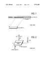
- FIG. 1 is an illustration of a normalization process of a typical normalization shifter found in the Prior Art.
- FIG. 2 is a general block diagram of a typical normalization shifter found in the Prior Art.
- FIG. 3 is a general block diagram of the normalization shifter in a floating point arithmetic unit of a microprocessor in accordance with the present invention.
- FIG. 4 is a general block diagram of a four level normalization shifter illustrating one embodiment of the present invention.
- FIG. 5 is a general block diagram of the sticky bit logic circuit of the 64-bit shifter of FIG. 4.
- FIG. 6 is a general block diagram of an alternative embodiment of the sticky bit logic circuit of the 16-bit shifter of FIG. 4.
- FIG. 7 is a general block diagram of the sticky bit logic circuit of FIG. 6.
- the present invention provides a method and apparatus to perform the computation of a sticky bit in a multistage shifter used for floating point arithmetic.
- the method can be used for both alignment and normalization processes.
- a normalization circuit is presented as one embodiment that performs the normalization of a number using multiple shifting stages in the floating point arithmetic unit of a microprocessor.
- the first shifter shifts in increments of 64 bits
- the second shifter shifts in increments of 16 bits
- the third shifter shifts in increments of 4 bits
- the fourth and final shifter shifts in increments of 1 bit.
- the first shifter initially receives the unnormalized number and shifts in increments of 64 bits on a signal called the shift control.
- Each stage is coupled to a separate sticky bit logic circuit.
- the sticky bit can be computed in parallel to the shifting at any particular stage.
- the last stage is the stage where the last shifting sequence was performed on the number.
- the sticky bit is computed in this alternative embodiment using the data inputs of the first shifter, the control inputs of the first shifter and the control inputs of the second shifter.
- the sticky bit can be calculated at the second stage without having to wait for the first stage of the normalization circuit to complete its process.
- FIGS. 1 through 6 of the drawings disclose various embodiments of the present invention for purposes of illustration.
- One skilled in the art will recognize alternative embodiments that may be employed without departing from the principles of the invention that are illustrated by the structures and methods described herein.
- use of the method set forth below in the form of an alignment shifter would still embody the basic principals of the present invention.
- the normalization shifter 10 receives a 192-bit binary input number 12. This is the number to be normalized. As can be seen in FIG. 3, the input 12 is the output of the Carry Propagate Adder (CPA) 14. As can be seen in FIG. 1, the number can have a plurality of leading zeroes, a 1 representing the left most significant bit, a round bit representing the right most significant bit, intermediate significant bits between the round bit and the most significant bit and a sticky bit representing the ORed product of the bits to the right of the round bit.
- the normalization shifter output 16 is a 65-bit normalized number including a round bit.
- the normalization shifter 10 in FIG. 2 receives the input 12, which is the output from the CPA 14. Shifting of the input 12 is governed by a shift control circuit 18 which is within the Leading Bit Anticipator (LBA) 20 shown pictured in FIG. 3. This results in a 65-bit normalized output number at the final output 16 and a sticky bit output at sticky bit output 24.
- LBA Leading Bit Anticipator
- the particular parameters for the 192-bit numbers and the 65 bit numbers referred to herein pertain to a particular embodiment for illustration and can be changed to conform to a variety of scenarios calling for different parameters.
- the shifter itself can be implemented in a number of stages and is not limited to the four-stage shifter described herein. Changes to these parameters would not, however, depart from the spirit and scope of the present invention as described and claimed herein.
- the output of the Carry Save Adder (CSA) 26 are two binary numbers that are issued to the CPA 14 and the LBA 20.
- the CPA 14 performs an arithmetic function on the two numbers producing the 192-bit input number to the normalization shifter.
- the LBA 20 receives the same two numbers and predicts the number of leading zeroes resulting at the CPA 14 output.
- the normalization shifter 10 receives the 192-bit input from the output 15 of the CPA 14.
- the normalization shifter receives the 192-bit input number 12 from the CPA 14 and also receives control signals from the LBA 20 and shifts the input number in response thereto as described below.
- the normalization shifter 10 is a 4-stage shifter, each stage shifting the input number a predetermined increment, in response to the LBA 20, each stage outputting a sticky bit and each stage outputting a partially normalized number.
- the present embodiment disclosed herein is a four stage shifter, different implementations may call for more or less stages of different sizes. Different variations, however, would not vary from the spirit and scope of the present invention as described and claimed herein.
- the second shifter the 16 bit shifter 32
- the 64 bit shifter 30 would shift at a maximum of 192 bits. This is simply because the input number is a total of 192 bits.
- the first stage includes a 64-bit shifter 30 coupled to the first input 15, coupled to a first shift control 18A, coupled to a first output 16A and coupled to a first sticky bit logic circuit 40. Details of the sticky bit logic circuit for the 64-bit shifter are shown in FIG. 5.
- the first shifter 30 receives the 192-bit input number 12 and shifts the number in increments of 64-bits in response to inputting the number and in response to the first shifting control output 18A.
- the first shifter 30 shifts by 0, 64 or 128 bits in response to the first shift controller 18A.
- the output number necessarily has less than 64 consecutive leading zeroes and, since the final output is a 65 bit number including a round bit, the output 16A of the first shifter 30 can be reduced by 64 bits from the right most bit.
- the first shifter 30 then outputs the left most 128 bits to the next stage of the shifter after the shifting operation of the first shifter. For example, if the first shifter shifts the input data by zero, bits (63:0) cannot make it to the next stage and thus are ORed together with the OR gate 48 of the first sticky bit logic circuit 40 to participate in the sticky bit generation. If the shift count is greater than zero, the sticky bit of this stage is a zero.
- the final sticky bit is the result of the sticky bit logic outputs 24A through 24D ORed together with OR gate 50.
- the sticky bit at the final output 24 of the OR gate 50 will be ready before the shifting process is completed.
- subsequent stages will necessarily need to compute a sticky bit individually to ensure an accurate sticky bit computation.
- a key feature of this implementation is a reduction in hardware for computing the sticky bit without sacrificing performance. Subsequent stages in the multi-stage shifter 10 operate similarly.
- the second shifter 32 receives a 128 bit number from the first shifter output 16A of the first shifter 30. Similar to the first shifter, the second shifter 32 receives a 16-bit shifting signal from the second shift control output 18B of the LBA 20 and shifts the 128 bit number in response thereto. The second shifter shifts in increments of 0, 16, 32, or 48 bits. Like the first shifter 30, all the least significant bits that cannot make it to the next stage participate in the sticky bit generation.
- the output 16B of the second shifter 32 can be reduced by 48 bits. Therefore, the output number of the second shifter is 80 bits. The right most 48 bits which will be unused in the next stage of the shifter will be ORed together to produce the sticky bit. If this stage shifts by 16, then 32 bits are ORed if by 32, 16 bits are ORed and if by 48, 0 bits are ORed.
- Another embodiment of the present invention includes an alternate method with the related hardware to compute the sticky bit at the second stage of the multi-bit shifter that does not rely on the output of the first shifter 30.
- the sticky bit at the second stage can be computed from the data inputs to the first shifter, the control inputs of the first shifter and the control inputs of the second shifter. This is illustrated in FIG. 6.
- the logic circuit used to compute the sticky bit at the second stage of the multi-stage shifter is shown in FIG. 7.
- the left portion 60 of the circuit is utilized when there is no shift at the first shifter 30.
- the left most 128 bits that will have been input to the second shifter is analyzed by the left portion 60. If there is to be no 16 bit shift left at the second shifter, then the input number input ⁇ 111:64> will necessarily be ORed together to compute the sticky bit. Accordingly, the left portion 60 logically ANDs the result of ORing together the input ⁇ 111:64> with the shl16 0 (or no-shift by 16 bits). This result is then logically ANDed with the shl64 0 (or no-shift by 64 bits) to produce the sticky bit for the second shifter. The process is similar with a shift of 16 or 32 bits.
- the process for the right portion 61 of the circuit is engaged when there is a shl64 1 (or shift left 64 bits once).
- the process is similar to that of the left portion 60 except that the portion of the number ORed together is shifted by 64 bits. If there is no shift anticipated for the second shifter 32, the bits input ⁇ 47:0> are ORed together to compute the sticky bit. If there is one shift with the second shifter, then input ⁇ 31:0> is ORed and if there are two shifts then input ⁇ 15:0> is ORed.
- the second shifter 32 outputs a second partially normalized number for use in the third stage.
- the third shifter 34 receives an 80-bit number from the output 16B of the second shifter 32 and, similar to the first and second shifter, shifts the 80-bit number in increments of 4 bits or 0, 4, 8 or 12 bits in response to the third shift controller 18C of the LBA 20. Similar to the first and second shifter, if the third shifter 34 shifts the number by zero, a sticky bit is produced at this stage using the third sticky bit logic circuit 44 to produce a sticky bit at the third sticky bit output 24C. The right most 12 bits from the 80-bit number would then be ORed together to produce the sticky bit at the third stage if the shift amount is zero.
- the third shifter 34 shifts by 4, 8 bits are ORed, if it shifts by 8, 4 bits are ORed and if it shifts by 12, 0 bits are ORed.
- the output 16C of the third shifter 34 can be reduced by 12 bits. Therefore, the output 16C of the third shifter is 68 bits.
- the third shifter outputs a partially normalized 68-bit number at the third output 16C that is available for the next stage.
- the fourth shifter 36 receives the 68-bit number from the fourth shifter output 16C and shifts the number in increments of 1 bit in response to the fourth shift controller 18B in the LBA 20. Again, similar to the first three stages, if the fourth shifter shifts by zero, the remaining 3 unused bits are ORed together to produce the sticky bit using the fourth sticky bit logic circuit 46 which is output at the fourth sticky bit output and ORed together with the other sticky bit outputs 24A through 24C to produce the final sticky bit 24. If the fourth shifter shifts by 1, 2 bits are ORed, if by 2, 1 bit is ORed, if by 3, 0 bits are ORed. The final normalized number is output by the fourth shifter at the fourth shifter output 16D. This is a 65-bit normalized number.
- the first shifter In the first stage, the first shifter inputs the 192-bit number. Since there are less than 64 zeroes leading the left most significant bit, there is no shift at this stage.
- the right most 64 bits (63:0) are ORed together with the first sticky bit logic circuit 40 to produce a sticky bit at the first sticky bit output 24A. Since there are 1's in the right most bits being ORed, a sticky bit is produced.
- the sticky bit is received by the OR gate 50 producing a sticky bit 24. Thus, we now have a sticky bit before the number is completely normalized.
- the first shifter 30 then outputs the left most 128 bits.
- the second shifter 32 receives the 128-bit number. Since there are 18 leading zeroes in the number, the second shifter 32 shifts 16 bits to the left. The least significant 32 bits are then ORed to produce a sticky bit. This second shifter then outputs the left most 80 bits of the number.
- the third shifter 34 receives the 80-bit number. No shift occurs because there are less than four leading zeroes at this point.
- the right most 12 bits are ORed together to produce the sticky bit with the third sticky bit logic circuit 44 and a sticky bit output is produced at the third sticky bit output 24C.
- the third shifter then outputs the left most 68 bits of the number.
- the fourth shifter receives the 68-bit number.
- the shifter shifts twice in response to the fourth shift controller 18B since there are two leading zeroes left.
- the single right most bit is ORed to produce a sticky bit.
- the fourth shifter 36 then outputs the left most 65-bits of the number producing the final normalized number.
- the sticky bit is already waiting to further computations.
- the first shifter 30 inputs the 192-bit number.
- the number is shifted 64-bits to the left since there are 64 leading zeroes. No sticky bit is produced because there was a shift.
- the sticky bit can be produced.
- the general block diagram showing the process utilizing alternate sticky logic 42' is shown in FIG. 6 with the details of the sticky bit logic circuit 24B' illustrated in FIG. 7. Since there is a shift at stage 1, the right most portion illustrated in FIG. 7 is utilized.
- the input bits input ⁇ 47:0> from the input are ORed together.
- the result is then ANDed with the 16-bit or second shifting signal shl16 0 at the AND gate 52.
- This second result then ORed with the other shl16 ANDed combinations at the OR gate 54.
- This third result is then ANDed with the 64 bit shifting signal from the first shift control signal at AND gate 56 and finally ORed together at OR gate 58 with the left section of FIG. 7 to produce the sticky bit from the second stage.
Abstract
Description
Claims (18)
Priority Applications (1)
| Application Number | Priority Date | Filing Date | Title |
|---|---|---|---|
| US08/672,678 US5771183A (en) | 1996-06-28 | 1996-06-28 | Apparatus and method for computation of sticky bit in a multi-stage shifter used for floating point arithmetic |
Applications Claiming Priority (1)
| Application Number | Priority Date | Filing Date | Title |
|---|---|---|---|
| US08/672,678 US5771183A (en) | 1996-06-28 | 1996-06-28 | Apparatus and method for computation of sticky bit in a multi-stage shifter used for floating point arithmetic |
Publications (1)
| Publication Number | Publication Date |
|---|---|
| US5771183A true US5771183A (en) | 1998-06-23 |
Family
ID=24699554
Family Applications (1)
| Application Number | Title | Priority Date | Filing Date |
|---|---|---|---|
| US08/672,678 Expired - Lifetime US5771183A (en) | 1996-06-28 | 1996-06-28 | Apparatus and method for computation of sticky bit in a multi-stage shifter used for floating point arithmetic |
Country Status (1)
| Country | Link |
|---|---|
| US (1) | US5771183A (en) |
Cited By (17)
| Publication number | Priority date | Publication date | Assignee | Title |
|---|---|---|---|---|
| WO1999060475A1 (en) * | 1998-05-19 | 1999-11-25 | Intel Corporation | A leading bit anticipator for floating point multiplication |
| US5999960A (en) * | 1995-04-18 | 1999-12-07 | International Business Machines Corporation | Block-normalization in multiply-add floating point sequence without wait cycles |
| US6085211A (en) * | 1997-02-13 | 2000-07-04 | Kabushiki Kaisha Toshiba | Logic circuit and floating-point arithmetic unit |
| WO2001004724A2 (en) * | 1999-07-12 | 2001-01-18 | Sony Electronics, Inc. | A partitioned shift right logic circuit having rounding support |
| US20020078109A1 (en) * | 2000-12-19 | 2002-06-20 | Nec Corporation | Shift and detecting circuit and floating-point calculating circuit using the same |
| US20020198916A1 (en) * | 2001-05-21 | 2002-12-26 | Graham Kirsch | Method and circuit for normalization of floating point significands in a SIMD array MPP |
| US6557021B1 (en) * | 1999-11-04 | 2003-04-29 | Intrinsity, Inc. | Rounding anticipator for floating point operations |
| US6571267B1 (en) | 1999-03-10 | 2003-05-27 | Kabushiki Kaisha Toshiba | Floating point addition/subtraction execution unit |
| US20040210610A1 (en) * | 2002-12-12 | 2004-10-21 | Adaptec, Inc. | Method and apparatus for aligning operands for a processor |
| US20040254971A1 (en) * | 2003-06-11 | 2004-12-16 | Stmicroelectronics, Inc. | Method and system for computing alignment sticky bit in floating-point operations |
| US20060101108A1 (en) * | 2004-11-05 | 2006-05-11 | International Business Machines Corporation | Using a leading-sign anticipator circuit for detecting sticky-bit information |
| US20070050434A1 (en) * | 2005-08-25 | 2007-03-01 | Arm Limited | Data processing apparatus and method for normalizing a data value |
| US20070130242A1 (en) * | 2005-12-02 | 2007-06-07 | Fujitsu Limited | Arithmetic operation unit, information processing apparatus and arithmetic operation method |
| JP2012521047A (en) * | 2009-03-16 | 2012-09-10 | アドバンスト・マイクロ・ディバイシズ・インコーポレイテッド | Mechanism for fast detection of overshifts in floating point units |
| US20130018933A1 (en) * | 2010-03-31 | 2013-01-17 | Telefonaktiebolaget Lm Ericsson (Publ) | Data Shifter and Control Method Thereof, Multiplexer, Data Sifter, and Data Sorter |
| RU2498392C1 (en) * | 2012-07-20 | 2013-11-10 | Открытое акционерное общество "КОНСТРУКТОРСКОЕ БЮРО "КОРУНД-М" (ОАО КБ "КОРУНД-М") | Device to predict exceptional situation "accuracy loss" of "multiplication with accumulation" operation unit |
| US20140181170A1 (en) * | 2012-12-26 | 2014-06-26 | Kabushiki Kaisha Toshiba | Arithmetic circuit and arithmetic method |
Citations (4)
| Publication number | Priority date | Publication date | Assignee | Title |
|---|---|---|---|---|
| US4782457A (en) * | 1986-08-18 | 1988-11-01 | Texas Instruments Incorporated | Barrel shifter using bit reversers and having automatic normalization |
| US4887232A (en) * | 1987-05-15 | 1989-12-12 | Digital Equipment Corporation | Apparatus and method for performing a shift operation in a multiplier array circuit |
| US4901263A (en) * | 1988-09-12 | 1990-02-13 | General Electric Company | Versatile data shifter with sticky bit generation capability |
| US4999796A (en) * | 1989-12-14 | 1991-03-12 | Motorola, Inc. | Sticky bit detection and shifting logic |
-
1996
- 1996-06-28 US US08/672,678 patent/US5771183A/en not_active Expired - Lifetime
Patent Citations (4)
| Publication number | Priority date | Publication date | Assignee | Title |
|---|---|---|---|---|
| US4782457A (en) * | 1986-08-18 | 1988-11-01 | Texas Instruments Incorporated | Barrel shifter using bit reversers and having automatic normalization |
| US4887232A (en) * | 1987-05-15 | 1989-12-12 | Digital Equipment Corporation | Apparatus and method for performing a shift operation in a multiplier array circuit |
| US4901263A (en) * | 1988-09-12 | 1990-02-13 | General Electric Company | Versatile data shifter with sticky bit generation capability |
| US4999796A (en) * | 1989-12-14 | 1991-03-12 | Motorola, Inc. | Sticky bit detection and shifting logic |
Cited By (30)
| Publication number | Priority date | Publication date | Assignee | Title |
|---|---|---|---|---|
| US5999960A (en) * | 1995-04-18 | 1999-12-07 | International Business Machines Corporation | Block-normalization in multiply-add floating point sequence without wait cycles |
| US6085211A (en) * | 1997-02-13 | 2000-07-04 | Kabushiki Kaisha Toshiba | Logic circuit and floating-point arithmetic unit |
| WO1999060475A1 (en) * | 1998-05-19 | 1999-11-25 | Intel Corporation | A leading bit anticipator for floating point multiplication |
| US6571267B1 (en) | 1999-03-10 | 2003-05-27 | Kabushiki Kaisha Toshiba | Floating point addition/subtraction execution unit |
| WO2001004724A2 (en) * | 1999-07-12 | 2001-01-18 | Sony Electronics, Inc. | A partitioned shift right logic circuit having rounding support |
| WO2001004724A3 (en) * | 1999-07-12 | 2001-08-09 | Sony Electronics Inc | A partitioned shift right logic circuit having rounding support |
| US6557021B1 (en) * | 1999-11-04 | 2003-04-29 | Intrinsity, Inc. | Rounding anticipator for floating point operations |
| US20020078109A1 (en) * | 2000-12-19 | 2002-06-20 | Nec Corporation | Shift and detecting circuit and floating-point calculating circuit using the same |
| EP1220086A2 (en) * | 2000-12-19 | 2002-07-03 | Nec Corporation | Shift circuits and partial sticky bit detection for floating point calculation |
| EP1220086A3 (en) * | 2000-12-19 | 2002-07-17 | Nec Corporation | Shift circuits and partial sticky bit detection for floating point calculation |
| US20020198916A1 (en) * | 2001-05-21 | 2002-12-26 | Graham Kirsch | Method and circuit for normalization of floating point significands in a SIMD array MPP |
| US6981012B2 (en) * | 2001-05-21 | 2005-12-27 | Micron Technology, Inc. | Method and circuit for normalization of floating point significants in a SIMD array MPP |
| US20040210610A1 (en) * | 2002-12-12 | 2004-10-21 | Adaptec, Inc. | Method and apparatus for aligning operands for a processor |
| US7320013B2 (en) * | 2002-12-12 | 2008-01-15 | Adaptec, Inc. | Method and apparatus for aligning operands for a processor |
| US20040254971A1 (en) * | 2003-06-11 | 2004-12-16 | Stmicroelectronics, Inc. | Method and system for computing alignment sticky bit in floating-point operations |
| US8543632B2 (en) * | 2003-06-11 | 2013-09-24 | Stmicroelectronics, Inc. | Method and system for computing alignment sticky bit in floating-point operations |
| US20060101108A1 (en) * | 2004-11-05 | 2006-05-11 | International Business Machines Corporation | Using a leading-sign anticipator circuit for detecting sticky-bit information |
| US7668892B2 (en) * | 2005-08-25 | 2010-02-23 | Arm Limited | Data processing apparatus and method for normalizing a data value |
| US20070050434A1 (en) * | 2005-08-25 | 2007-03-01 | Arm Limited | Data processing apparatus and method for normalizing a data value |
| EP1806652A3 (en) * | 2005-12-02 | 2008-11-05 | Fujitsu Ltd. | Normalization and rounding of an arithmetic operation result |
| JP2007156748A (en) * | 2005-12-02 | 2007-06-21 | Fujitsu Ltd | Arithmetic processor, information processor and arithmetic processing method |
| US20070130242A1 (en) * | 2005-12-02 | 2007-06-07 | Fujitsu Limited | Arithmetic operation unit, information processing apparatus and arithmetic operation method |
| US7720899B2 (en) | 2005-12-02 | 2010-05-18 | Fujitsu Limited | Arithmetic operation unit, information processing apparatus and arithmetic operation method |
| JP4571903B2 (en) * | 2005-12-02 | 2010-10-27 | 富士通株式会社 | Arithmetic processing apparatus, information processing apparatus, and arithmetic processing method |
| EP1806652A2 (en) | 2005-12-02 | 2007-07-11 | Fujitsu Ltd. | Normalization and rounding of an arithmetic operation result |
| JP2012521047A (en) * | 2009-03-16 | 2012-09-10 | アドバンスト・マイクロ・ディバイシズ・インコーポレイテッド | Mechanism for fast detection of overshifts in floating point units |
| US20130018933A1 (en) * | 2010-03-31 | 2013-01-17 | Telefonaktiebolaget Lm Ericsson (Publ) | Data Shifter and Control Method Thereof, Multiplexer, Data Sifter, and Data Sorter |
| RU2498392C1 (en) * | 2012-07-20 | 2013-11-10 | Открытое акционерное общество "КОНСТРУКТОРСКОЕ БЮРО "КОРУНД-М" (ОАО КБ "КОРУНД-М") | Device to predict exceptional situation "accuracy loss" of "multiplication with accumulation" operation unit |
| US20140181170A1 (en) * | 2012-12-26 | 2014-06-26 | Kabushiki Kaisha Toshiba | Arithmetic circuit and arithmetic method |
| US9632751B2 (en) * | 2012-12-26 | 2017-04-25 | Kabushiki Kaisha Toshiba | Arithmetic circuit and arithmetic method |
Similar Documents
| Publication | Publication Date | Title |
|---|---|---|
| US5771183A (en) | Apparatus and method for computation of sticky bit in a multi-stage shifter used for floating point arithmetic | |
| US5696711A (en) | Apparatus and method for performing variable precision floating point rounding operations | |
| US5889690A (en) | Multiply-add unit and data processing apparatus using it | |
| EP0127988B1 (en) | A normalizing circuit | |
| US5844830A (en) | Executing computer instrucrions by circuits having different latencies | |
| US7395304B2 (en) | Method and apparatus for performing single-cycle addition or subtraction and comparison in redundant form arithmetic | |
| US5600583A (en) | Circuit and method for detecting if a sum of two multidigit numbers equals a third multidigit number prior to availability of the sum | |
| US20210349692A1 (en) | Multiplier and multiplication method | |
| US5426598A (en) | Adder and multiplier circuit employing the same | |
| US5204825A (en) | Method and apparatus for exact leading zero prediction for a floating-point adder | |
| EP1806652B1 (en) | Normalization and rounding of an arithmetic operation result | |
| US5367477A (en) | Method and apparatus for performing parallel zero detection in a data processing system | |
| JPH0542011B2 (en) | ||
| US6988119B2 (en) | Fast single precision floating point accumulator using base 32 system | |
| US5790445A (en) | Method and system for performing a high speed floating point add operation | |
| US5260889A (en) | Computation of sticky-bit in parallel with partial products in a floating point multiplier unit | |
| JPH0545982B2 (en) | ||
| US5867413A (en) | Fast method of floating-point multiplication and accumulation | |
| US5245563A (en) | Fast control for round unit | |
| US4677583A (en) | Apparatus for decimal multiplication | |
| US5754458A (en) | Trailing bit anticipator | |
| EP0361886B1 (en) | Improved floating point computation unit | |
| US5570309A (en) | Iterative arithmetic processor | |
| US5781464A (en) | Apparatus and method for incrementing floating-point numbers represented in diffrent precision modes | |
| US5635858A (en) | Zero-stopping incrementers |
Legal Events
| Date | Code | Title | Description |
|---|---|---|---|
| AS | Assignment |
Owner name: INTEL CORPORATION, CALIFORNIA Free format text: ASSIGNMENT OF ASSIGNORS INTEREST;ASSIGNOR:MAKINENI, SIVAKUMAR;REEL/FRAME:008151/0757 Effective date: 19960826 |
|
| STCF | Information on status: patent grant |
Free format text: PATENTED CASE |
|
| FPAY | Fee payment |
Year of fee payment: 4 |
|
| REMI | Maintenance fee reminder mailed | ||
| FPAY | Fee payment |
Year of fee payment: 8 |
|
| FPAY | Fee payment |
Year of fee payment: 12 |
|
| AS | Assignment |
Owner name: MICRON TECHNOLOGY, INC., IDAHO Free format text: ASSIGNMENT OF ASSIGNORS INTEREST;ASSIGNOR:INTEL CORPORATION;REEL/FRAME:030747/0001 Effective date: 20111122 |
|
| AS | Assignment |
Owner name: U.S. BANK NATIONAL ASSOCIATION, AS COLLATERAL AGENT, CALIFORNIA Free format text: SECURITY INTEREST;ASSIGNOR:MICRON TECHNOLOGY, INC.;REEL/FRAME:038669/0001 Effective date: 20160426 Owner name: U.S. BANK NATIONAL ASSOCIATION, AS COLLATERAL AGEN Free format text: SECURITY INTEREST;ASSIGNOR:MICRON TECHNOLOGY, INC.;REEL/FRAME:038669/0001 Effective date: 20160426 |
|
| AS | Assignment |
Owner name: MORGAN STANLEY SENIOR FUNDING, INC., AS COLLATERAL AGENT, MARYLAND Free format text: PATENT SECURITY AGREEMENT;ASSIGNOR:MICRON TECHNOLOGY, INC.;REEL/FRAME:038954/0001 Effective date: 20160426 Owner name: MORGAN STANLEY SENIOR FUNDING, INC., AS COLLATERAL Free format text: PATENT SECURITY AGREEMENT;ASSIGNOR:MICRON TECHNOLOGY, INC.;REEL/FRAME:038954/0001 Effective date: 20160426 |
|
| AS | Assignment |
Owner name: U.S. BANK NATIONAL ASSOCIATION, AS COLLATERAL AGENT, CALIFORNIA Free format text: CORRECTIVE ASSIGNMENT TO CORRECT THE REPLACE ERRONEOUSLY FILED PATENT #7358718 WITH THE CORRECT PATENT #7358178 PREVIOUSLY RECORDED ON REEL 038669 FRAME 0001. ASSIGNOR(S) HEREBY CONFIRMS THE SECURITY INTEREST;ASSIGNOR:MICRON TECHNOLOGY, INC.;REEL/FRAME:043079/0001 Effective date: 20160426 Owner name: U.S. BANK NATIONAL ASSOCIATION, AS COLLATERAL AGEN Free format text: CORRECTIVE ASSIGNMENT TO CORRECT THE REPLACE ERRONEOUSLY FILED PATENT #7358718 WITH THE CORRECT PATENT #7358178 PREVIOUSLY RECORDED ON REEL 038669 FRAME 0001. ASSIGNOR(S) HEREBY CONFIRMS THE SECURITY INTEREST;ASSIGNOR:MICRON TECHNOLOGY, INC.;REEL/FRAME:043079/0001 Effective date: 20160426 |
|
| AS | Assignment |
Owner name: MICRON TECHNOLOGY, INC., IDAHO Free format text: RELEASE BY SECURED PARTY;ASSIGNOR:U.S. BANK NATIONAL ASSOCIATION, AS COLLATERAL AGENT;REEL/FRAME:047243/0001 Effective date: 20180629 |
|
| AS | Assignment |
Owner name: MICRON TECHNOLOGY, INC., IDAHO Free format text: RELEASE BY SECURED PARTY;ASSIGNOR:MORGAN STANLEY SENIOR FUNDING, INC., AS COLLATERAL AGENT;REEL/FRAME:050937/0001 Effective date: 20190731 |