US5766426A - Apparatus for, and method of, depositing a film on a substrate - Google Patents
Apparatus for, and method of, depositing a film on a substrate Download PDFInfo
- Publication number
- US5766426A US5766426A US08/388,475 US38847595A US5766426A US 5766426 A US5766426 A US 5766426A US 38847595 A US38847595 A US 38847595A US 5766426 A US5766426 A US 5766426A
- Authority
- US
- United States
- Prior art keywords
- anode
- substrate
- target
- voltage
- deposition
- Prior art date
- Legal status (The legal status is an assumption and is not a legal conclusion. Google has not performed a legal analysis and makes no representation as to the accuracy of the status listed.)
- Expired - Fee Related
Links
Images


Classifications
-
- H—ELECTRICITY
- H01—ELECTRIC ELEMENTS
- H01J—ELECTRIC DISCHARGE TUBES OR DISCHARGE LAMPS
- H01J37/00—Discharge tubes with provision for introducing objects or material to be exposed to the discharge, e.g. for the purpose of examination or processing thereof
- H01J37/32—Gas-filled discharge tubes
- H01J37/34—Gas-filled discharge tubes operating with cathodic sputtering
- H01J37/3411—Constructional aspects of the reactor
- H01J37/3438—Electrodes other than cathode
-
- C—CHEMISTRY; METALLURGY
- C23—COATING METALLIC MATERIAL; COATING MATERIAL WITH METALLIC MATERIAL; CHEMICAL SURFACE TREATMENT; DIFFUSION TREATMENT OF METALLIC MATERIAL; COATING BY VACUUM EVAPORATION, BY SPUTTERING, BY ION IMPLANTATION OR BY CHEMICAL VAPOUR DEPOSITION, IN GENERAL; INHIBITING CORROSION OF METALLIC MATERIAL OR INCRUSTATION IN GENERAL
- C23C—COATING METALLIC MATERIAL; COATING MATERIAL WITH METALLIC MATERIAL; SURFACE TREATMENT OF METALLIC MATERIAL BY DIFFUSION INTO THE SURFACE, BY CHEMICAL CONVERSION OR SUBSTITUTION; COATING BY VACUUM EVAPORATION, BY SPUTTERING, BY ION IMPLANTATION OR BY CHEMICAL VAPOUR DEPOSITION, IN GENERAL
- C23C14/00—Coating by vacuum evaporation, by sputtering or by ion implantation of the coating forming material
- C23C14/04—Coating on selected surface areas, e.g. using masks
- C23C14/046—Coating cavities or hollow spaces, e.g. interior of tubes; Infiltration of porous substrates
-
- C—CHEMISTRY; METALLURGY
- C23—COATING METALLIC MATERIAL; COATING MATERIAL WITH METALLIC MATERIAL; CHEMICAL SURFACE TREATMENT; DIFFUSION TREATMENT OF METALLIC MATERIAL; COATING BY VACUUM EVAPORATION, BY SPUTTERING, BY ION IMPLANTATION OR BY CHEMICAL VAPOUR DEPOSITION, IN GENERAL; INHIBITING CORROSION OF METALLIC MATERIAL OR INCRUSTATION IN GENERAL
- C23C—COATING METALLIC MATERIAL; COATING MATERIAL WITH METALLIC MATERIAL; SURFACE TREATMENT OF METALLIC MATERIAL BY DIFFUSION INTO THE SURFACE, BY CHEMICAL CONVERSION OR SUBSTITUTION; COATING BY VACUUM EVAPORATION, BY SPUTTERING, BY ION IMPLANTATION OR BY CHEMICAL VAPOUR DEPOSITION, IN GENERAL
- C23C14/00—Coating by vacuum evaporation, by sputtering or by ion implantation of the coating forming material
- C23C14/22—Coating by vacuum evaporation, by sputtering or by ion implantation of the coating forming material characterised by the process of coating
- C23C14/34—Sputtering
- C23C14/35—Sputtering by application of a magnetic field, e.g. magnetron sputtering
-
- C—CHEMISTRY; METALLURGY
- C23—COATING METALLIC MATERIAL; COATING MATERIAL WITH METALLIC MATERIAL; CHEMICAL SURFACE TREATMENT; DIFFUSION TREATMENT OF METALLIC MATERIAL; COATING BY VACUUM EVAPORATION, BY SPUTTERING, BY ION IMPLANTATION OR BY CHEMICAL VAPOUR DEPOSITION, IN GENERAL; INHIBITING CORROSION OF METALLIC MATERIAL OR INCRUSTATION IN GENERAL
- C23C—COATING METALLIC MATERIAL; COATING MATERIAL WITH METALLIC MATERIAL; SURFACE TREATMENT OF METALLIC MATERIAL BY DIFFUSION INTO THE SURFACE, BY CHEMICAL CONVERSION OR SUBSTITUTION; COATING BY VACUUM EVAPORATION, BY SPUTTERING, BY ION IMPLANTATION OR BY CHEMICAL VAPOUR DEPOSITION, IN GENERAL
- C23C14/00—Coating by vacuum evaporation, by sputtering or by ion implantation of the coating forming material
- C23C14/22—Coating by vacuum evaporation, by sputtering or by ion implantation of the coating forming material characterised by the process of coating
- C23C14/54—Controlling or regulating the coating process
- C23C14/541—Heating or cooling of the substrates
-
- H—ELECTRICITY
- H01—ELECTRIC ELEMENTS
- H01J—ELECTRIC DISCHARGE TUBES OR DISCHARGE LAMPS
- H01J37/00—Discharge tubes with provision for introducing objects or material to be exposed to the discharge, e.g. for the purpose of examination or processing thereof
- H01J37/32—Gas-filled discharge tubes
- H01J37/34—Gas-filled discharge tubes operating with cathodic sputtering
- H01J37/3402—Gas-filled discharge tubes operating with cathodic sputtering using supplementary magnetic fields
-
- H—ELECTRICITY
- H01—ELECTRIC ELEMENTS
- H01J—ELECTRIC DISCHARGE TUBES OR DISCHARGE LAMPS
- H01J2237/00—Discharge tubes exposing object to beam, e.g. for analysis treatment, etching, imaging
- H01J2237/20—Positioning, supporting, modifying or maintaining the physical state of objects being observed or treated
- H01J2237/2001—Maintaining constant desired temperature
Definitions
- This invention relates to a system for, and a method of, controlling the characteristics of the deposition on a substrate such as a wafer for integrated circuit chips or a magnetic transducer head. More particularly, this invention relates to a system for, and a method of, regulating the temperature of such a substrate so that a deposition with optimal characteristics can be provided on the substrate.
- Wafers are fabricated with a plurality of dies (sometimes as many as hundreds) on each wafer. Each of the dies on a wafer subsequently forms an integrated circuit chip. The dies are tested while on the wafer to determine if they have been produced properly. The defective dies are marked to distinguish then from the satisfactory dies. The dies are then cut from the wafer and the satisfactory dies are retained for use as integrated circuit chips.
- the wafers are produced from a plurality of successive layers, some of them formed electrically conductive material and others formed from electrically insulating material.
- a layer of an electrically conductive material When a layer of an electrically conductive material is formed, it generally is produced in a pattern to represent electrical circuitry.
- a layer of an electrically conductive material is initially deposited on the wafer, hopefully in a substantially uniform thickness.
- the layer is then masked with a material which is subjected to light in a pattern corresponding to the pattern of the electrical circuitry to be produced.
- the masking material subjected to the light is impervious to an etching material such as an acid.
- the remaining portions of the layer are then etched as by an acid.
- the masking material subjected to the light is then removed from the remaining electrically conductive material in the layer.
- the electrically conductive material remaining in such layer is then joined with the electrically conductive material in other layers to define the electrical circuitry for each die on the wafer.
- Apparatus has been in use for some time for depositing sputtered atoms on a wafer to produce a layer of material defined by the sputtered atoms.
- the apparatus now in use produces such a deposition by providing a glow discharge between an anode and a target in a cavity to obtain an emission of sputtered atoms from the target.
- a magnetic field co-operates with the electrical field providing the glow discharge to produce a force on the electrons for enhancing the movement of the electrons in the cavity between the target and the anode. This enhanced movement of the electrons facilitates the ionization of the neutral gas.
- the target when a layer of aluminum is to be deposited on a wafer, the target may be made from aluminum.
- the target is bombarded with ions of an inert gas such as argon, the target emits sputtered atoms of aluminum. These sputtered atoms travel to the wafer and become deposited on the wafer to produce a substantially uniform layer of electrically conductive material on the wafer such as discussed in the previous paragraph.
- the deposition may be provided with a substantially uniform thickness on the surface of the substrate and on the walls of grooves in the substrate.
- a deposition with such characteristics may be provided in grooves in the substrate when the voltage on the anode is approximately forty five volts (+45V.) and the target has a negative voltage of approximately four hundred and fifty five volts (-455V.).
- the anode is at a positive potential of approximately two hundred volts (+200V.) and the target is at a negative potential of approximately three hundred volts (-300 V.)
- the deposition tends to fill the grooves and provide a substantially smooth surface with the remaining surface on the wafer.
- the glow discharge adjacent the anode has approximately the voltage of the anode. This causes the sputtered atoms emitted from the target to travel with a relatively high energy to the substrate and to impinge on the substrate with such a high energy. This high energy impingement causes the temperature of the substrate to rise. It has been found that it is not desirable for the temperature of the substrate to rise above a value such as approximately 450° C. Above that temperature, the substrate tends to deteriorate.
- This invention provides a system for, and a method of, regulating the temperature of the substrate during the deposition of materials on the substrate so that the substrate temperature does not increase above approximately 450° C.
- the system and method of this invention provide such a regulation in a relatively simple and straight forward manner. In this way, the characteristics of the depositions on the substrate are maintained on an optimal basis.
- an electrical field between a positive anode and a negative target in a cavity and a magnetic field in the cavity cause electrons from the target to ionize neutral gas (e.g. argon) atoms in the cavity.
- the ions cause the target to release sputtered atoms (e.g. aluminum) for deposition on a substrate.
- a shield between the target and the substrate inhibits charged particle movement to the substrate.
- the anode potential may be positive, and the shield and the magnetic members may be negative relative to the anode, to obtain electron movement to the anode, thereby inhibiting the heating of the shield and the magnetic members by electron impingement.
- the anode may be water cooled.
- the magnitude of the positive anode voltage relative to the target voltage provides selectively for (a) a uniform thickness of sputtered atoms on the walls of a groove in the substrate or (b) a filling of the groove by the sputtered atoms and a uniform thickness of deposition on the substrate surface including the filled groove.
- a sensor may receive infra red energy passing from the substrate through a hole in the anode to provide signals having characteristics indicating variations in the substrate temperature.
- the anode voltage is varied in accordance with the characteristics of such signal to regulate the temperature of the substrate.
- the target voltage is preferably varied with the anode voltage variations to maintain the anode-cathode voltage difference substantially a constant.
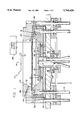
- FIG. 1 is a fragmentary sectional view, in side elevation, of apparatus constituting one embodiment of the apparatus for depositing sputtered atoms of a material from a target on a surface of a substrate such as a wafer and on the walls of grooves in such surface;
- FIG. 2 is a top plan view of the embodiment shown in FIG. 1;
- FIG. 3 is an enlarged elevational view schematically illustrating a substrate, and the grooves in a surface of the substrate, receiving the deposition of the sputtered atoms;
- FIG. 4 illustrates on an enlarged fragmentary basis a groove in a substrate and a deposition of a substantially uniform thickness on the walls of the groove and, on the substrate by apparatus shown in FIGS. 1 and 2;
- FIG. 5 illustrates on an enlarged fragmentary basis a groove in a substrate and a deposition to fill the substrate and to provide a substantially uniform thickness on the substrate and the area including the groove, this deposition being provided by apparatus shown in FIGS. 1 and 2;
- FIG. 6 shows curves illustrating (a) current to the substrate for progressive values of voltage on the substrate and (b) current to the substrate for progressive voltage differences between the anode and the substrate;
- FIG. 7 is a schematic diagram of a system constituting one embodiment of the invention for regulating the temperature of the substrate so that the depositions on the substrate will have optimal characteristics.
- apparatus generally indicated at 10 in FIG. 1 is provided for depositing sputtered atoms from a target 12 onto a substrate 14.
- the substrate may constitute a wafer 14 which is used in the semiconductor industry.
- the wafer 14 may be disposed at a ground potential.
- the wafer 14 may be in the form of a thin disc made from a suitable material such as silicon dioxide and having a suitable diameter such as approximately five inches (5").
- the wafer may hold a plurality of dies, each of generally identical construction and each forming, when completed, an integrated circuit chip defining complex electrical circuitry.
- Each die 15 may be quite small (e.g. 1/4" ⁇ 1/4") so that a considerable number of dies can be formed on a single wafer.
- Each die 15 may be provided with a surface 17 for receiving a uniform deposition of sputtered atoms and may be further provided with grooves 19 in such surface.
- the walls of the grooves 19 are also expected to receive a deposition of the sputtered atoms. In many instances, the deposition of the sputtered atoms on the walls of the grooves 19 is expected to be in a substantially uniform thickness.
- the target 12 may be a unitary member, preferably with an annular configuration, as shown in FIGS. 1 and 2.
- the target 12 may be defined by an annular external periphery 16 and may be provided with a centrally disposed opening defining a frusto-conical internal periphery 18.
- the internal periphery 18 of the target 12 may have a frusto-conical configuration.
- the target 12 may be made from a suitable material such as aluminum or titanium.
- An anode 32 is disposed internally relative to the target 12 and may be supported in any suitable manner well known in the art.
- a chamber or cavity 34 is defined in part by the target 12.
- the cavity 34 holds atoms of an inert gas such as argon.
- the atoms of the inert gas such as argon are introduced to the cavity 34 through an inlet 35.
- An electrical field is provided between the anode 32 and the target 12 by connecting the anode and the targets respectively to the positive and negative terminals of a power supply 36.
- the anode 32 may be at ground potential or some suitable voltage above ground and the target 12 may be at a negative potential.
- a clamp 40 is disposed in the central opening of the target 12 in abutting relationship with the internal periphery 18 of the target.
- the clamp 40 has a shoulder which overlays the internal periphery 18 of the target 12.
- the clamp 40 may be made from a suitable material such as copper.
- the clamp 40 is disposed against a support portion 44 of a cooling member 46 and is attached to the support portion of the cooling member as by screws.
- the cooling member 46 has a portion 50 which abuts the external periphery 16 of the target 12.
- a passageway 52 is respectively disposed in the cooling member 46 and externally of the cooling member to provide for the flow of a fluid such as water to cool the clamp 40 and the target 12.
- a pair of magnetizable members 54 and 55 enclosing a permanent magnet 56 are disposed on opposite sides of the target 12 to create a magnetic field in the cavity 34.
- the magnetizable members 54 and 55 and the permanent magnet 56 may be at a ground potential.
- the voltage difference between the anode 32 and the target 12 causes electrons from the discharge to travel toward the anode.
- the electrons move in a spiral path from the target 12 toward the anode 32 because the magnetic field produced in the cavity or chamber 34 by the permanent magnet 56 and the magnetizable members 54 and 55 has a force vector component in a direction perpendicular to the electrical field between the anode and the target. Because of this spiral path, the electrons have an ample opportunity to strike and ionize argon atoms in the cavity or chamber 34.
- the argon ions travel to the frusto-conical internal periphery 18 of the target 12 and cause sputtered atoms to be released from this surface when they impinge on such surface.
- the sputtered atoms travel to the wafer 14 and become deposited on the wafer.
- the target becomes progressively worn.
- the target 12 is removed from the apparatus and is replaced by a new target.
- the target becomes heated. This would tend to cause the target to expand at its external periphery 16 in FIG. 1 because of metal expansion caused by heat.
- the external periphery 16 of the target 12 is maintained in fixed position by its mechanical abutment with the portion 50 of the cooling member 46 and by the cooling action of the cooling member. This cooling action results from the flow of a cooling fluid such as water through the passageway 52.
- a shield 70 made from a suitable material such as aluminum is disposed between the target 12 and the wafer 14.
- the shield 70 is provided with a hollow interior 72 having a suitable configuration such as a frusto-conical configuration defining a funnel with progressive positions toward the wafer 14.
- the shield 70 may be provided with a suitable potential such as a ground potential.
- the shield 70 attracts electrons and negative ions in the space between the target 12 and the wafer 14. Since the charged particles produce heat when they impinge upon the wafer 14, the inhibition provided by the shield 70 against the movement of the charged particles to the wafer 14 causes the wafer to be maintained at a relatively cool temperature relative to the temperature of wafers in apparatus of the prior art. This allows the wafer 14 to be disposed closer to the target 12 than in the apparatus of the prior art.
- the sputtered atoms from the target can be deposited on the wafer 14 with a greater density than in the apparatus of the prior art. Furthermore, the sputtered atoms can be deposited on the wafer 14 with an enhanced uniformity of thickness relative to the deposition of the sputtered atoms on the wafer by the apparatus of the prior art.
- the voltage difference between the target 12 and the anode 32 may be as much as five hundred volts (500V.).
- the voltage on the anode 32 may be varied, with an inverse variation of the voltage on the target 12, to affect the characteristics of the deposition on the wafer 14.
- a deposition 68 of a substantially constant thickness is made on the walls 72 of a groove 74 in the wafer 14 as illustrated schematically in FIG. 4.
- a deposition of a substantially uniform thickness is also provided on the smooth surface of the wafer 14 as illustrated schematically at 76 in FIG. 4. This is advantageous because it has been difficult, if not impossible, to provide a deposition of a uniform thickness on the walls of a groove such as the groove 74 on the adjacent surface 76 in the prior art by using a single target.
- a deposition 78 tends to fill the groove 74 and to provide a substantially smooth surface 79 of the wafer 14 and in the area formerly occupied by the groove 74. This is indicated schematically in FIG. 5. It has been difficult, if not impossible, to accomplish this in the prior art.
- a glow discharge of charged particles accumulates near the anode 32.
- This glow discharge may be produced in part from charged particles of argon when the argon is ionized by the electrons from the glow discharge.
- This glow discharge has a potential approaching that of the anode 32. For example, when the target 12 is at a negative potential of five hundred volts (-500V.) and the anode 32 is at substantially a ground potential, the glow discharge may be at a negative potential of approximately two volts (-2V.).
- the glow discharge may be at a potential close to approximately one hundred volts when the anode 32 is at a positive potential of approximately one hundred volts (+100V.) and the target 12 is at a negative potential of four hundred volts (-400V.).
- the ions formed in the glow discharge are attracted toward the wafer 14.
- the potential of the glow discharge is dependent upon the voltage on the anode.
- the potential difference between the glow discharge and the wafer 14 affects the characteristics of the deposition on the walls 72 of the groove 74 in the wafer 14 and on the smooth surface 76 of the wafer 14 as discussed in the previous paragraph.
- a curve 120 illustrates the relationship between changes in voltage on the substrate such as the wafer 14 relative to the current flowing to the wafer in milliamperes. This current indicates the rate of deposition of the sputtered atoms on the substrate 14.
- the curve 120 in FIG. 6 indicates that the current flow to the substrate 14 becomes substantially saturated when the negative voltage on the substrate 14 reaches a relatively low negative value such as approximately five volts (-5V.).
- a curve 122 in FIG. 6 indicates the relationship between the voltage on the anode 32 (shown on the horizontal axis) and the current flowing to the substrate 14 in milliamperes (shown on the vertical axis).
- the voltage on the horizontal axis is shown relative to a ground potential on the substrate 14.
- the current flowing to the substrate 14 continues to increase for anode voltages considerably in excess of five volts (5V.).
- Such measurements have been made to anode voltages of approximately sixty volts (+60V.).
- This relationship is further advantageous in that the current increase is substantially linear in the range to approximately sixty volts (+60V.) in the potential on the anode 32.
- the curve 122 shows a space charge limited current with no indication of saturation.
- the rate of deposition of the sputtered atoms on the wafer is relatively large when the anode has a potential which is relatively high.
- the temperature of the wafer 14 affects the characteristics of the wafer when the temperature exceeds a particular value such as approximately 450° C. Above this temperature, the wafer 14 tends to deteriorate.
- This invention provides a system as shown schematically in FIG. 7 for regulating the temperature of the substrate so that the substrate temperature does not exceed 450° C. and preferably does not exceed a temperature which is uncomfortably close to 450° C.
- the system includes the substrate or wafer 14 and the anode 32.
- a hole 100 is provided in the anode 32 to pass infra red energy from the substrate or wafer.
- the magnitude of the infra red energy passing through the hole 100 in the anode 32 is dependent upon the temperature of the substrate or wafer 14.
- the infrared energy passing through the hole 100 is received by an infra red detector 102 which thus produces a signal with a magnitude dependent upon the temperature of the wafer 14.
- the signal on the detector 102 is introduced to a regulator 104 (shown as a central processing unit in FIG. 7) which varies the voltage on the anode 32 and the target 12 in accordance with variations in the magnitude of the signal from the detector 102.
- the voltage on the anode 32 is reduced when the temperature on the wafer 32 approaches approximately 450° C., thereby reducing the temperature of the substrate. In this way, the temperature of the wafer 32 is regulated so that it does not exceed a temperature of approximately 450° C.
Abstract
Description
Claims (35)
Priority Applications (1)
| Application Number | Priority Date | Filing Date | Title |
|---|---|---|---|
| US08/388,475 US5766426A (en) | 1995-02-14 | 1995-02-14 | Apparatus for, and method of, depositing a film on a substrate |
Applications Claiming Priority (1)
| Application Number | Priority Date | Filing Date | Title |
|---|---|---|---|
| US08/388,475 US5766426A (en) | 1995-02-14 | 1995-02-14 | Apparatus for, and method of, depositing a film on a substrate |
Publications (1)
| Publication Number | Publication Date |
|---|---|
| US5766426A true US5766426A (en) | 1998-06-16 |
Family
ID=23534265
Family Applications (1)
| Application Number | Title | Priority Date | Filing Date |
|---|---|---|---|
| US08/388,475 Expired - Fee Related US5766426A (en) | 1995-02-14 | 1995-02-14 | Apparatus for, and method of, depositing a film on a substrate |
Country Status (1)
| Country | Link |
|---|---|
| US (1) | US5766426A (en) |
Cited By (7)
| Publication number | Priority date | Publication date | Assignee | Title |
|---|---|---|---|---|
| KR19990023327A (en) * | 1997-08-05 | 1999-03-25 | 토마스 엠. 알바레즈 | Apparatus and method for depositing first and second materials onto a substrate |
| US6110337A (en) * | 1997-12-01 | 2000-08-29 | National Research Council Of Canada | Sputtering method and apparatus with optical monitoring |
| FR2797944A1 (en) * | 1999-08-27 | 2001-03-02 | Sleever Int | FOUR-TUNNEL WITH INFRARED ELEMENTS |
| US20040244949A1 (en) * | 2003-05-30 | 2004-12-09 | Tokyo Electron Limited | Temperature controlled shield ring |
| CN103074579A (en) * | 2011-10-26 | 2013-05-01 | 塔工程有限公司 | Thin film deposition apparatus |
| US20130156937A1 (en) * | 2011-12-16 | 2013-06-20 | Intermolecular, Inc. | System and Method for Aligning Sputter Sources |
| CN106884150A (en) * | 2017-04-24 | 2017-06-23 | 大连爱瑞德纳米科技有限公司 | A kind of suspension anode and the magnetic control sputtering device with suspension anode |
Citations (7)
| Publication number | Priority date | Publication date | Assignee | Title |
|---|---|---|---|---|
| US4100055A (en) * | 1977-06-10 | 1978-07-11 | Varian Associates, Inc. | Target profile for sputtering apparatus |
| US4913790A (en) * | 1988-03-25 | 1990-04-03 | Tokyo Electron Limited | Treating method |
| US4994162A (en) * | 1989-09-29 | 1991-02-19 | Materials Research Corporation | Planarization method |
| US5080772A (en) * | 1990-08-24 | 1992-01-14 | Materials Research Corporation | Method of improving ion flux distribution uniformity on a substrate |
| US5108570A (en) * | 1990-03-30 | 1992-04-28 | Applied Materials, Inc. | Multistep sputtering process for forming aluminum layer over stepped semiconductor wafer |
| US5126028A (en) * | 1989-04-17 | 1992-06-30 | Materials Research Corporation | Sputter coating process control method and apparatus |
| US5135634A (en) * | 1991-02-14 | 1992-08-04 | Sputtered Films, Inc. | Apparatus for depositing a thin layer of sputtered atoms on a member |
-
1995
- 1995-02-14 US US08/388,475 patent/US5766426A/en not_active Expired - Fee Related
Patent Citations (7)
| Publication number | Priority date | Publication date | Assignee | Title |
|---|---|---|---|---|
| US4100055A (en) * | 1977-06-10 | 1978-07-11 | Varian Associates, Inc. | Target profile for sputtering apparatus |
| US4913790A (en) * | 1988-03-25 | 1990-04-03 | Tokyo Electron Limited | Treating method |
| US5126028A (en) * | 1989-04-17 | 1992-06-30 | Materials Research Corporation | Sputter coating process control method and apparatus |
| US4994162A (en) * | 1989-09-29 | 1991-02-19 | Materials Research Corporation | Planarization method |
| US5108570A (en) * | 1990-03-30 | 1992-04-28 | Applied Materials, Inc. | Multistep sputtering process for forming aluminum layer over stepped semiconductor wafer |
| US5080772A (en) * | 1990-08-24 | 1992-01-14 | Materials Research Corporation | Method of improving ion flux distribution uniformity on a substrate |
| US5135634A (en) * | 1991-02-14 | 1992-08-04 | Sputtered Films, Inc. | Apparatus for depositing a thin layer of sputtered atoms on a member |
Cited By (8)
| Publication number | Priority date | Publication date | Assignee | Title |
|---|---|---|---|---|
| KR19990023327A (en) * | 1997-08-05 | 1999-03-25 | 토마스 엠. 알바레즈 | Apparatus and method for depositing first and second materials onto a substrate |
| US6110337A (en) * | 1997-12-01 | 2000-08-29 | National Research Council Of Canada | Sputtering method and apparatus with optical monitoring |
| FR2797944A1 (en) * | 1999-08-27 | 2001-03-02 | Sleever Int | FOUR-TUNNEL WITH INFRARED ELEMENTS |
| WO2001016543A1 (en) * | 1999-08-27 | 2001-03-08 | Sleever International Company | Tunnel kiln with infrared elements |
| US20040244949A1 (en) * | 2003-05-30 | 2004-12-09 | Tokyo Electron Limited | Temperature controlled shield ring |
| CN103074579A (en) * | 2011-10-26 | 2013-05-01 | 塔工程有限公司 | Thin film deposition apparatus |
| US20130156937A1 (en) * | 2011-12-16 | 2013-06-20 | Intermolecular, Inc. | System and Method for Aligning Sputter Sources |
| CN106884150A (en) * | 2017-04-24 | 2017-06-23 | 大连爱瑞德纳米科技有限公司 | A kind of suspension anode and the magnetic control sputtering device with suspension anode |
Similar Documents
| Publication | Publication Date | Title |
|---|---|---|
| US5135634A (en) | Apparatus for depositing a thin layer of sputtered atoms on a member | |
| US4853102A (en) | Sputtering process and an apparatus for carrying out the same | |
| US5234560A (en) | Method and device for sputtering of films | |
| US4401539A (en) | Sputtering cathode structure for sputtering apparatuses, method of controlling magnetic flux generated by said sputtering cathode structure, and method of forming films by use of said sputtering cathode structure | |
| KR900004600B1 (en) | Setting target and target set of magnetron sputter | |
| US4675530A (en) | Charge density detector for beam implantation | |
| US7288166B2 (en) | Plasma processing apparatus | |
| JPH02274874A (en) | Apparatus and method for sputtering for coating and piling of base sheet | |
| TWI284916B (en) | Method and device for producing extreme ultraviolet radiation and soft x-ray radiation | |
| SE430188B (en) | METHOD OF JON IMPLANTATION FOR MANAGING THE SURFACE POTENTIAL OF A TEMPLE, AND DEVICE FOR APPLICATION OF THE METHOD | |
| US4392932A (en) | Method for obtaining uniform etch by modulating bias on extension member around radio frequency etch table | |
| US5766426A (en) | Apparatus for, and method of, depositing a film on a substrate | |
| JPS62228463A (en) | Magnetron sputtering apparatus having separation limit magnetic field separating target and magnetically intensified r.f. bias | |
| US3282815A (en) | Magnetic control of film deposition | |
| JP2000311890A (en) | Plasma etching method and device | |
| US3325394A (en) | Magnetic control of film deposition | |
| US20040007183A1 (en) | Apparatus and method for the formation of thin films | |
| EP0544831B1 (en) | Sputtering apparatus and sputtering method of improving ion flux distribution uniformity on a substrate | |
| EP0413291B1 (en) | Method and device for sputtering of films | |
| US8791433B2 (en) | Ion implanting apparatus | |
| US6605198B1 (en) | Apparatus for, and method of, depositing a film on a substrate | |
| US6620301B1 (en) | Method for forming a sputtered layer and apparatus therefor | |
| Strümpel et al. | Dynamics of zigzag destabilized solitary stripes in a dc-driven pattern-forming semiconductor gas-discharge system | |
| Paik et al. | The characterization of a magnetron-sputter-type negative-ion source | |
| US20240145206A1 (en) | Temperature controlled electrode to limit deposition rates and distortion |
Legal Events
| Date | Code | Title | Description |
|---|---|---|---|
| AS | Assignment |
Owner name: SPUTTERED FILMS, INC., CALIFORNIA Free format text: ASSIGNMENT OF ASSIGNORS INTEREST;ASSIGNOR:CLARKE, ANDREW P.;REEL/FRAME:007452/0499 Effective date: 19950125 |
|
| AS | Assignment |
Owner name: UNION BANK, CALIFORNIA Free format text: SECURITY AGREEMENT;ASSIGNOR:SPUTTERED FILMS INC.;REEL/FRAME:007764/0336 Effective date: 19951214 |
|
| AS | Assignment |
Owner name: FINOVA CAPITAL CORPORATION, CALIFORNIA Free format text: SECURITY AGREEMENT;ASSIGNOR:SPUTTERED FILMS, INC.;REEL/FRAME:008766/0855 Effective date: 19971028 |
|
| AS | Assignment |
Owner name: FINOVA CAPITAL CORPORATION, CALIFORNIA Free format text: SECURITY INTEREST;ASSIGNOR:SPUTTERED FILMS, INC.;REEL/FRAME:009808/0010 Effective date: 19990304 |
|
| FEPP | Fee payment procedure |
Free format text: PAYOR NUMBER ASSIGNED (ORIGINAL EVENT CODE: ASPN); ENTITY STATUS OF PATENT OWNER: SMALL ENTITY |
|
| REMI | Maintenance fee reminder mailed | ||
| LAPS | Lapse for failure to pay maintenance fees | ||
| STCH | Information on status: patent discontinuation |
Free format text: PATENT EXPIRED DUE TO NONPAYMENT OF MAINTENANCE FEES UNDER 37 CFR 1.362 |
|
| FP | Lapsed due to failure to pay maintenance fee |
Effective date: 20020616 |