US5763914A - Cell topology for power transistors with increased packing density - Google Patents
Cell topology for power transistors with increased packing density Download PDFInfo
- Publication number
- US5763914A US5763914A US08/895,507 US89550797A US5763914A US 5763914 A US5763914 A US 5763914A US 89550797 A US89550797 A US 89550797A US 5763914 A US5763914 A US 5763914A
- Authority
- US
- United States
- Prior art keywords
- cell
- transistor cell
- gate
- trenched
- recited
- Prior art date
- Legal status (The legal status is an assumption and is not a legal conclusion. Google has not performed a legal analysis and makes no representation as to the accuracy of the status listed.)
- Expired - Lifetime
Links
- 238000012856 packing Methods 0.000 title abstract description 29
- 229910021420 polycrystalline silicon Inorganic materials 0.000 claims abstract description 60
- 229920005591 polysilicon Polymers 0.000 claims abstract description 59
- 239000000758 substrate Substances 0.000 claims abstract description 41
- 210000000746 body region Anatomy 0.000 claims abstract description 17
- 239000004065 semiconductor Substances 0.000 claims abstract description 10
- 239000012535 impurity Substances 0.000 claims abstract description 6
- 239000002019 doping agent Substances 0.000 claims description 7
- 210000004027 cell Anatomy 0.000 description 151
- 238000004519 manufacturing process Methods 0.000 description 20
- 238000000034 method Methods 0.000 description 14
- 230000008569 process Effects 0.000 description 12
- 238000009792 diffusion process Methods 0.000 description 10
- 238000012545 processing Methods 0.000 description 6
- XUIMIQQOPSSXEZ-UHFFFAOYSA-N Silicon Chemical compound [Si] XUIMIQQOPSSXEZ-UHFFFAOYSA-N 0.000 description 4
- 239000007943 implant Substances 0.000 description 4
- 229910052710 silicon Inorganic materials 0.000 description 4
- 239000010703 silicon Substances 0.000 description 4
- 238000005530 etching Methods 0.000 description 3
- 230000004907 flux Effects 0.000 description 3
- 230000006872 improvement Effects 0.000 description 3
- 238000010884 ion-beam technique Methods 0.000 description 3
- 229910052751 metal Inorganic materials 0.000 description 3
- 239000002184 metal Substances 0.000 description 3
- 238000001465 metallisation Methods 0.000 description 3
- 230000009467 reduction Effects 0.000 description 3
- 229910052785 arsenic Inorganic materials 0.000 description 2
- RQNWIZPPADIBDY-UHFFFAOYSA-N arsenic atom Chemical compound [As] RQNWIZPPADIBDY-UHFFFAOYSA-N 0.000 description 2
- 239000005380 borophosphosilicate glass Substances 0.000 description 2
- 210000003850 cellular structure Anatomy 0.000 description 2
- 238000013461 design Methods 0.000 description 2
- 230000000694 effects Effects 0.000 description 2
- 238000012986 modification Methods 0.000 description 2
- 230000004048 modification Effects 0.000 description 2
- 230000003647 oxidation Effects 0.000 description 2
- 238000007254 oxidation reaction Methods 0.000 description 2
- 238000002179 total cell area Methods 0.000 description 2
- ZOXJGFHDIHLPTG-UHFFFAOYSA-N Boron Chemical compound [B] ZOXJGFHDIHLPTG-UHFFFAOYSA-N 0.000 description 1
- OAICVXFJPJFONN-UHFFFAOYSA-N Phosphorus Chemical compound [P] OAICVXFJPJFONN-UHFFFAOYSA-N 0.000 description 1
- 238000001994 activation Methods 0.000 description 1
- 229910052782 aluminium Inorganic materials 0.000 description 1
- XAGFODPZIPBFFR-UHFFFAOYSA-N aluminium Chemical compound [Al] XAGFODPZIPBFFR-UHFFFAOYSA-N 0.000 description 1
- 230000000903 blocking effect Effects 0.000 description 1
- 229910052796 boron Inorganic materials 0.000 description 1
- 230000015556 catabolic process Effects 0.000 description 1
- 230000008859 change Effects 0.000 description 1
- 238000011109 contamination Methods 0.000 description 1
- 230000003247 decreasing effect Effects 0.000 description 1
- 238000000280 densification Methods 0.000 description 1
- 239000003989 dielectric material Substances 0.000 description 1
- 230000005669 field effect Effects 0.000 description 1
- 238000002513 implantation Methods 0.000 description 1
- 239000011261 inert gas Substances 0.000 description 1
- 238000005468 ion implantation Methods 0.000 description 1
- 150000002500 ions Chemical class 0.000 description 1
- 229910044991 metal oxide Inorganic materials 0.000 description 1
- 150000004706 metal oxides Chemical class 0.000 description 1
- 238000004806 packaging method and process Methods 0.000 description 1
- 230000003071 parasitic effect Effects 0.000 description 1
- 229910052698 phosphorus Inorganic materials 0.000 description 1
- 239000011574 phosphorus Substances 0.000 description 1
- 229910021332 silicide Inorganic materials 0.000 description 1
- FVBUAEGBCNSCDD-UHFFFAOYSA-N silicide(4-) Chemical compound [Si-4] FVBUAEGBCNSCDD-UHFFFAOYSA-N 0.000 description 1
Images


Classifications
-
- H—ELECTRICITY
- H01—ELECTRIC ELEMENTS
- H01L—SEMICONDUCTOR DEVICES NOT COVERED BY CLASS H10
- H01L29/00—Semiconductor devices adapted for rectifying, amplifying, oscillating or switching, or capacitors or resistors with at least one potential-jump barrier or surface barrier, e.g. PN junction depletion layer or carrier concentration layer; Details of semiconductor bodies or of electrodes thereof ; Multistep manufacturing processes therefor
- H01L29/66—Types of semiconductor device ; Multistep manufacturing processes therefor
- H01L29/66007—Multistep manufacturing processes
- H01L29/66075—Multistep manufacturing processes of devices having semiconductor bodies comprising group 14 or group 13/15 materials
- H01L29/66227—Multistep manufacturing processes of devices having semiconductor bodies comprising group 14 or group 13/15 materials the devices being controllable only by the electric current supplied or the electric potential applied, to an electrode which does not carry the current to be rectified, amplified or switched, e.g. three-terminal devices
- H01L29/66409—Unipolar field-effect transistors
- H01L29/66477—Unipolar field-effect transistors with an insulated gate, i.e. MISFET
- H01L29/66674—DMOS transistors, i.e. MISFETs with a channel accommodating body or base region adjoining a drain drift region
- H01L29/66712—Vertical DMOS transistors, i.e. VDMOS transistors
-
- H—ELECTRICITY
- H01—ELECTRIC ELEMENTS
- H01L—SEMICONDUCTOR DEVICES NOT COVERED BY CLASS H10
- H01L29/00—Semiconductor devices adapted for rectifying, amplifying, oscillating or switching, or capacitors or resistors with at least one potential-jump barrier or surface barrier, e.g. PN junction depletion layer or carrier concentration layer; Details of semiconductor bodies or of electrodes thereof ; Multistep manufacturing processes therefor
- H01L29/02—Semiconductor bodies ; Multistep manufacturing processes therefor
- H01L29/06—Semiconductor bodies ; Multistep manufacturing processes therefor characterised by their shape; characterised by the shapes, relative sizes, or dispositions of the semiconductor regions ; characterised by the concentration or distribution of impurities within semiconductor regions
- H01L29/0684—Semiconductor bodies ; Multistep manufacturing processes therefor characterised by their shape; characterised by the shapes, relative sizes, or dispositions of the semiconductor regions ; characterised by the concentration or distribution of impurities within semiconductor regions characterised by the shape, relative sizes or dispositions of the semiconductor regions or junctions between the regions
- H01L29/0692—Surface layout
- H01L29/0696—Surface layout of cellular field-effect devices, e.g. multicellular DMOS transistors or IGBTs
-
- H—ELECTRICITY
- H01—ELECTRIC ELEMENTS
- H01L—SEMICONDUCTOR DEVICES NOT COVERED BY CLASS H10
- H01L29/00—Semiconductor devices adapted for rectifying, amplifying, oscillating or switching, or capacitors or resistors with at least one potential-jump barrier or surface barrier, e.g. PN junction depletion layer or carrier concentration layer; Details of semiconductor bodies or of electrodes thereof ; Multistep manufacturing processes therefor
- H01L29/66—Types of semiconductor device ; Multistep manufacturing processes therefor
- H01L29/68—Types of semiconductor device ; Multistep manufacturing processes therefor controllable by only the electric current supplied, or only the electric potential applied, to an electrode which does not carry the current to be rectified, amplified or switched
- H01L29/76—Unipolar devices, e.g. field effect transistors
- H01L29/772—Field effect transistors
- H01L29/78—Field effect transistors with field effect produced by an insulated gate
- H01L29/7801—DMOS transistors, i.e. MISFETs with a channel accommodating body or base region adjoining a drain drift region
- H01L29/7802—Vertical DMOS transistors, i.e. VDMOS transistors
- H01L29/7811—Vertical DMOS transistors, i.e. VDMOS transistors with an edge termination structure
-
- H—ELECTRICITY
- H01—ELECTRIC ELEMENTS
- H01L—SEMICONDUCTOR DEVICES NOT COVERED BY CLASS H10
- H01L29/00—Semiconductor devices adapted for rectifying, amplifying, oscillating or switching, or capacitors or resistors with at least one potential-jump barrier or surface barrier, e.g. PN junction depletion layer or carrier concentration layer; Details of semiconductor bodies or of electrodes thereof ; Multistep manufacturing processes therefor
- H01L29/66—Types of semiconductor device ; Multistep manufacturing processes therefor
- H01L29/68—Types of semiconductor device ; Multistep manufacturing processes therefor controllable by only the electric current supplied, or only the electric potential applied, to an electrode which does not carry the current to be rectified, amplified or switched
- H01L29/76—Unipolar devices, e.g. field effect transistors
- H01L29/772—Field effect transistors
- H01L29/78—Field effect transistors with field effect produced by an insulated gate
- H01L29/7801—DMOS transistors, i.e. MISFETs with a channel accommodating body or base region adjoining a drain drift region
- H01L29/7802—Vertical DMOS transistors, i.e. VDMOS transistors
- H01L29/7813—Vertical DMOS transistors, i.e. VDMOS transistors with trench gate electrode, e.g. UMOS transistors
-
- H—ELECTRICITY
- H01—ELECTRIC ELEMENTS
- H01L—SEMICONDUCTOR DEVICES NOT COVERED BY CLASS H10
- H01L29/00—Semiconductor devices adapted for rectifying, amplifying, oscillating or switching, or capacitors or resistors with at least one potential-jump barrier or surface barrier, e.g. PN junction depletion layer or carrier concentration layer; Details of semiconductor bodies or of electrodes thereof ; Multistep manufacturing processes therefor
- H01L29/02—Semiconductor bodies ; Multistep manufacturing processes therefor
- H01L29/06—Semiconductor bodies ; Multistep manufacturing processes therefor characterised by their shape; characterised by the shapes, relative sizes, or dispositions of the semiconductor regions ; characterised by the concentration or distribution of impurities within semiconductor regions
- H01L29/0603—Semiconductor bodies ; Multistep manufacturing processes therefor characterised by their shape; characterised by the shapes, relative sizes, or dispositions of the semiconductor regions ; characterised by the concentration or distribution of impurities within semiconductor regions characterised by particular constructional design considerations, e.g. for preventing surface leakage, for controlling electric field concentration or for internal isolations regions
- H01L29/0607—Semiconductor bodies ; Multistep manufacturing processes therefor characterised by their shape; characterised by the shapes, relative sizes, or dispositions of the semiconductor regions ; characterised by the concentration or distribution of impurities within semiconductor regions characterised by particular constructional design considerations, e.g. for preventing surface leakage, for controlling electric field concentration or for internal isolations regions for preventing surface leakage or controlling electric field concentration
- H01L29/0611—Semiconductor bodies ; Multistep manufacturing processes therefor characterised by their shape; characterised by the shapes, relative sizes, or dispositions of the semiconductor regions ; characterised by the concentration or distribution of impurities within semiconductor regions characterised by particular constructional design considerations, e.g. for preventing surface leakage, for controlling electric field concentration or for internal isolations regions for preventing surface leakage or controlling electric field concentration for increasing or controlling the breakdown voltage of reverse biased devices
- H01L29/0615—Semiconductor bodies ; Multistep manufacturing processes therefor characterised by their shape; characterised by the shapes, relative sizes, or dispositions of the semiconductor regions ; characterised by the concentration or distribution of impurities within semiconductor regions characterised by particular constructional design considerations, e.g. for preventing surface leakage, for controlling electric field concentration or for internal isolations regions for preventing surface leakage or controlling electric field concentration for increasing or controlling the breakdown voltage of reverse biased devices by the doping profile or the shape or the arrangement of the PN junction, or with supplementary regions, e.g. junction termination extension [JTE]
- H01L29/0619—Semiconductor bodies ; Multistep manufacturing processes therefor characterised by their shape; characterised by the shapes, relative sizes, or dispositions of the semiconductor regions ; characterised by the concentration or distribution of impurities within semiconductor regions characterised by particular constructional design considerations, e.g. for preventing surface leakage, for controlling electric field concentration or for internal isolations regions for preventing surface leakage or controlling electric field concentration for increasing or controlling the breakdown voltage of reverse biased devices by the doping profile or the shape or the arrangement of the PN junction, or with supplementary regions, e.g. junction termination extension [JTE] with a supplementary region doped oppositely to or in rectifying contact with the semiconductor containing or contacting region, e.g. guard rings with PN or Schottky junction
-
- H—ELECTRICITY
- H01—ELECTRIC ELEMENTS
- H01L—SEMICONDUCTOR DEVICES NOT COVERED BY CLASS H10
- H01L29/00—Semiconductor devices adapted for rectifying, amplifying, oscillating or switching, or capacitors or resistors with at least one potential-jump barrier or surface barrier, e.g. PN junction depletion layer or carrier concentration layer; Details of semiconductor bodies or of electrodes thereof ; Multistep manufacturing processes therefor
- H01L29/02—Semiconductor bodies ; Multistep manufacturing processes therefor
- H01L29/06—Semiconductor bodies ; Multistep manufacturing processes therefor characterised by their shape; characterised by the shapes, relative sizes, or dispositions of the semiconductor regions ; characterised by the concentration or distribution of impurities within semiconductor regions
- H01L29/0603—Semiconductor bodies ; Multistep manufacturing processes therefor characterised by their shape; characterised by the shapes, relative sizes, or dispositions of the semiconductor regions ; characterised by the concentration or distribution of impurities within semiconductor regions characterised by particular constructional design considerations, e.g. for preventing surface leakage, for controlling electric field concentration or for internal isolations regions
- H01L29/0607—Semiconductor bodies ; Multistep manufacturing processes therefor characterised by their shape; characterised by the shapes, relative sizes, or dispositions of the semiconductor regions ; characterised by the concentration or distribution of impurities within semiconductor regions characterised by particular constructional design considerations, e.g. for preventing surface leakage, for controlling electric field concentration or for internal isolations regions for preventing surface leakage or controlling electric field concentration
- H01L29/0638—Semiconductor bodies ; Multistep manufacturing processes therefor characterised by their shape; characterised by the shapes, relative sizes, or dispositions of the semiconductor regions ; characterised by the concentration or distribution of impurities within semiconductor regions characterised by particular constructional design considerations, e.g. for preventing surface leakage, for controlling electric field concentration or for internal isolations regions for preventing surface leakage or controlling electric field concentration for preventing surface leakage due to surface inversion layer, e.g. with channel stopper
-
- H—ELECTRICITY
- H01—ELECTRIC ELEMENTS
- H01L—SEMICONDUCTOR DEVICES NOT COVERED BY CLASS H10
- H01L29/00—Semiconductor devices adapted for rectifying, amplifying, oscillating or switching, or capacitors or resistors with at least one potential-jump barrier or surface barrier, e.g. PN junction depletion layer or carrier concentration layer; Details of semiconductor bodies or of electrodes thereof ; Multistep manufacturing processes therefor
- H01L29/40—Electrodes ; Multistep manufacturing processes therefor
- H01L29/402—Field plates
Definitions
- This invention relates generally to the structure and fabrication process of integrated circuit (IC) power transistors. More particularly, this invention relates to a novel and improved cell topology to achieve higher packing density which is defined as total channel width per unit cell area, to improve the current conduction of the power transistors.
- IC integrated circuit
- MOSFET metal oxide silicon field effect transistor
- conventional planar cellular structure of power MOSFETs such as square, circular, and hexagonal topologies are limited by the difficulty that the on-resistance is increased due to the reduction in polysilicon gate width which causes the JFET resistance to increase.
- the cell size is reduced in order to manufacture power device with higher cell density, the dimension of the cell and also width of the polysilicon gates are reduced. Since the on-resistance is inversely proportional to the width of the polysilicon gate, as the cell size is reduced, the width of the polysilicon gate is decreased and the on-resistance is increased.
- the requirement to maintain a low level of on-resistance becomes a major design difficulty and hindrance to manufacture power device with cell density higher than 6.5 million cells/in 2 since the increased JFET resistance cancels out the reduction in channel resistance when the unit cell size is shrunken.
- FIG. 1 shows a typical vertical double diffused MOS (VDMOS) device which uses a double diffusion technique to control the channel length 1.
- VDMOS vertical double diffused MOS
- Two successive diffusions are performed with first a p diffusion using boron, then a n+ diffusion using either arsenic or phosphorus, to produce two closely spaced pn junctions at different depths below the silicon surface.
- the VDMOS supports the drain voltage vertically in the n - epilayer. The current flows laterally from the source through the channel, parallel to the surface of the silicon.
- the current flow then turns through a right angle to flow vertically down through the drain epilayer to the substrate and to the drain contact.
- the current must first pass through the resistance of a parasitic JFET zone between two body-regions.
- the JFET resistance is inversely proportional to the width of the polysilicon gate. As the width of the polysilicon gate is reduced for the purpose of shrinking the size of the power transistor cells to obtain power device with higher cell density, the JFET resistance is increased.
- the power MOSFET device is fabricated by employing a cellular structure as that shown in FIGS. 2A and 2B.
- a cellular structure as that shown in FIGS. 2A and 2B.
- Several different schemes are used. High current capability is obtained by connecting many cells together in parallel as will be discussed below.
- heavily doped polycrystalline silicon is used as gate electrode.
- the connection metalization process where an oxide layer can be formed over the polysilicon and the source metalization may then be extended over the whole of the upper surface.
- the polysilicon, used as gate electrodes can be deposited with great accuracy and the gate oxide is more stable and less prone to contamination than the aluminum gate.
- the source is self aligned automatically with the gate edge thus greatly simplifies the fabrication process.
- FIGS. 2C and 2D shows the top views of two alternate square cell arrangements wherein the central dark squares represent the polysilicon gate and the outer squares represent the area occupied by the source region of each cell.
- the cell arrangement in FIG. 2C is commonly referred to as a "square on square” cell topology while that shown in FIG. 2D is a "square on hexagon" cell topology.
- the cell topology thus renders the three-dimensional diffusion phenomenon less problematic at the corners when the shallow junctions are formed for high density power transistor cells with channel length reduced to a range between 0.5 to 0.75 microns.
- Yilmez et al. disclose a solution to overcome the difficult in the square cells with corner vulnerability, the limitation of higher on-resistance with reduced cell size which commonly represented by a packing density parameter is still not resolved.
- the packing density is defined as: ##EQU1##
- the total channel width is 4a and the total cell area is (a+b) 2 .
- the packing density for this typical square cell is therefore:
- Another object of the present invention is to provide a new and improved MOSFET cell topology wherein the packing density is increased by manufacturing the transistor cells as non-orthogonal parallelograms with the sharper corner blunted or rounded whereby the packing density is increased with the same total channel width formed in a smaller cell area while the punch through vulnerability at the weak points in these sharper corners of the non-orthogonal parallelogram cells may be eliminated.
- Another object of the present invention is to provide a new and improved MOSFET cell topology wherein the packing density is increased by manufacturing the transistor cells as non-orthogonal parallelograms whereby the packing density is increased with the same total channel width formed in a smaller cell area while the processing flow employed in manufacturing the transistor cells can be applied without requiring significant changes thus greatly simplifying a switch over to the new transistor cell topology of this invention.
- the present invention includes a power transistor cell supported on a semiconductor substrate with a top surface and a bottom surface.
- the power transistor cell includes a drain region, doped with impurities of a first conductivity type, formed at the bottom surface.
- the power transistor cell further includes a polysilicon gate layer overlaying the top surface includes a polysilicon opening disposed substantially in a central portion of the transistor cell with a remaining portion of the polysilicon layer constituting a gate and defining an outer boundary for the transistor cell wherein the polysilicon opening and the outer boundary defined by the gate for the transistor cell constituting substantially non-orthogonal parallelograms.
- the power transistor further includes a source region, doped with the first conductivity type, disposed in the substrate underneath and around an outer edge of the source opening with a small portion extends underneath the gate.
- the power transistor further includes a body region, doped with a second conductivity type, disposed in the substrate surrounding the source region and an entire portion of the substrate underneath the polysilicon opening having a small portion extends underneath the gate near the cell boundary.
- the packing density of the transistor cell is improved with the parallelogram cell occupies less areas than the regular square cell having the same total channel width.
- FIG. 1 is a cross-sectional view of a prior art structure of a general MOSFET
- FIGS. 2A to 2B are partial perspective views of the layer structure of a prior art hexagonal and square MOSFET respectively;
- FIGS. 2C to 2D are top views of the prior art cell arrangements of the square MOSFET of FIG. 2B;
- FIGS. 3A and 3B show a top view and a cross sectional view of a prior art MOSFET cell topology and the packing density of the cell;
- FIGS. 4A and 4B show a top view and a cross sectional view of a MOSFET cell topology and the packing density of the cell of this invention
- FIG. 5A and 5B show the transistor cell arrangement respectively in parallelogram centered at lattice points of a hexagonal lattice and parallelogram centered at lattice points of a parallelogram lattice configuration;
- FIGS. 6A and 6B show the transistor cells with polysilicon openings have the sharp corners blunted and rounded respectively to remove punch through vulnerable points at the sharp corners of the parallelogram cells;
- FIGS. 7A and 7B show the transistor cell arrangement respectively in parallelogram centered at lattice points of a hexagonal lattice and parallelogram centered at lattice points of parallelogram lattice configurations of the blunted sharp-corner parallelogram cells;
- FIGS. 8A and 8B show the transistor cell arrangement respectively in parallelogram centered at lattice points of a hexagonal lattice and parallelogram centered at lattice points of a parallelogram lattice configurations of the rounded sharp-corner parallelogram cells;
- FIGS. 9A to 9D show the processing steps for manufacturing the MOSFET device of FIG. 3.
- FIGS. 10A and 10B show a top view and a cross sectional view of an array of trenched DMOS cells with improved packing density according to the cell topology disclosed in this invention.
- the transistor cells 100 are configured with a novel cell topology that the cell are formed to have a non-orthogonal parallelogram shape instead of the regular square, rectangular, or hexagonal shapes.
- the transistor cells 100 of parallelogram shape are formed to have the shaper corners opened between the horizontal and the tilted vertical boundary lines with an angle ⁇ which is less than 90-degrees, as that shown in FIGS. 4A and 4B.
- the packing density for the transistor cells 100 can be computed according the definition provided in Equation (1) as
- SIN ⁇ is always smaller or equal to 1.0
- the packing density for the transistor cell is increased. For example, if the sharper corners have a an angle of sixty-degrees, then there is about 16% improvement in packing density.
- a reduction of the total cell area of (a+b) 2 (1-SIN ⁇ ) can be achieved without sacrificing the total channel width which is maintained at the same value of 4a.
- the percentage of the improvement of the packing density for the transistor cell according to this invention can be computed as:
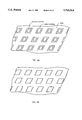
- the non-orthogonal parallelogram cells can be arranged in the configurations with either the parallelogram centered at lattice points of a hexagonal lattice or parallelogram centered at lattice points of a parallelogram lattice configuration as that shown in FIGS. 5A and 5B respectively.
- the non-orthogonal parallelogram cells can also be arranged as a parallelogram centered at lattice points of a square lattice configuration (not shown) depending on convenience of manufacture, packaging and device application considerations.
- the sharp corners of the polysilicon openings can be either blunted or rounded as that shown in FIGS. 6A and 6B respectively.
- the present invention achieves higher packing density by implementing a non-orthogonal parallelogram cell topology.
- the power transistor implemented with cell configuration of this invention can therefore be manufactured with higher cell density without sacrificing the total channel width because the cells of non-orthogonal parallelogram shapes occupy less total area than a regular square cell.
- FIGS. 7A and 7B for the power devices which include transistor cells of blunted non-orthogonal parallelogram cells arranged respectively in parallelogram centered at lattice points of a hexagonal lattice and parallelogram centered at lattice points of a parallelogram lattice configurations.
- FIGS. 8A and 8B illustrate the power devices which include transistor cells of rounded non-orthogonal parallelogram cells arranged respectively in parallelogram centered at lattice points of a hexagonal lattice and parallelogram centered at lattice points of a parallelogram lattice configurations.
- a power device includes a plurality of vertical MOSFET cells wherein each cell includes a drain disposed at a bottom surface of a substrate, a source region surrounded by a body region under a top surface of the substrate and a gate with a polysilicon opening disposed substantially near a center portion of the cell and overlaying a top surface of the substrate with a portion covering the source region and the body region thereunder wherein the polysilicon opening having a non-orthogonal parallelogram shape for each of the transistor cells.
- the transistor cells having the polysilicon opening of the non-orthogonal parallelogram shape are arranged with every four of the cells constituting substantially a non-orthogonal parallelogram shape.
- the transistor cells with the polysilicon opening of the non-orthogonal parallelogram shape are arranged with every four of the cells constituting sides of equal length. In a preferred embodiment, the transistor cells with the polysilicon opening of the non-orthogonal parallelogram shape are arranged with every seven of the cells constituting substantially a hexagonal shape including six outer cells defining a boundary of the hexagonal shape and one inner cell contained therein.
- the processing steps begins by first growing a N - epitaxial layer 110 with a resistivity ranging from 0.1 to 1.0 ohm-cm on top of a N+ substrate 105.
- the substrate has a resistivity of 0.001 to 0.007 ohm-cm.
- the thickness and the resistivity of the epitaxial layer 110 depend on the device requirements for the on-resistance and breakdown voltage. In a preferred embodiment, the thickness of the epi-layer 110 is about six to eight microns.
- An initial oxide layer 115 of thickness in the range of 5,000 to 10,000 ⁇ is grown which is then etched by applying a mask to define the active areas.
- a gate oxidation process is first carried out to form a gate oxide layer 120.
- a polysilicon layer 125 is then deposited on the gate oxide layer 120.
- a POCL 3 doping process is carried out followed by an arsenic (As) implant process with an ion beam of energy at 60-80 Kev with a flux density of 5 to 8 ⁇ 10 15 /cm 2 .
- a polysilicon mask is then applied to carry out the an anisotropic etching process to define the polysilicon gate 125 wherein the polysilicon gate 125 are formed with parallelogram shape as that shown in FIGS.
- 3A and 3B with a portion of the polysilicon layer 120 removed between adjacent core cells 102.
- the resist is then stripped and a p-body implant at 30-100 Kev with an ion beam of 3 ⁇ 10 13 to 3 ⁇ 10 14 /cm 2 flux density is applied to implant the p-body regions 130.
- a p-body diffusion process is then carried out at an elevated temperature of 1,000°-1,200° C. for ten minutes to increase the depth of the p-body region 120 to 1.0-2.0 ⁇ .
- a silicide layer 148 is then formed covering the top surface.
- a N+ block mask 135 is applied to carry out an N + implant to form the N + region 140.
- the N + implantation is carried out with an ion beam at an energy of 60-100 Kev and ion flux density of 5 ⁇ 10 15 to 1 ⁇ 10 16 /cm 2 .
- the resist i.e., the parallelogram-shaped N + blocking mask 135, is stripped, the N + source regions 140 are driven into desired junction depth ranging from 0.2 to 1.0 ⁇ by a diffusion process.
- a BPSG or PSG is deposited to form a layer 145 of approximately 5000-15,000 ⁇ in thickness.
- a BPSG flow or PSG densification process is performed at 900°-950° C.
- a contact mask is applied to perform an etching process to define the contact windows.
- a p+ ion implantation is carried out to form the p+ region 160 by a p+ activation process at 900°-950° C. in an oxidation or inert gas ambient.
- the final power MOSFET device 100 is completed with the metal deposition and metal etching with a metal mask to define the source contacts (S) 170, the gate contacts (G) 180, the field plate (FP) 185, and equal potential ring (EQR) 190. Since these metal contacts are well known in the art and are not the major features of this invention, they are not specifically described in details for the sake of simplicity and being more clearly focused on the main features of the invention.
- this invention discloses a power transistor cell 100 supported on a semiconductor substrate 105 with a top surface and a bottom surface.
- the power transistor cell includes a drain region, doped with impurities of a first conductivity type, formed at the bottom surface.
- the power transistor cell further includes a polysilicon gate layer overlaying the top surface includes a polysilicon opening disposed substantially in a central portion of the transistor cell with a remaining portion of the polysilicon layer constituting a gate and defining an outer boundary for the transistor cell wherein the polysilicon opening and the outer boundary defined by the gate for the transistor cell constituting substantially non-orthogonal parallelograms.
- the power transistor further includes a source region, doped with the first conductivity type, disposed in the substrate underneath and around an outer edge of the source opening with a small portion extends underneath the gate.
- the power transistor further includes a body region, doped with a second conductivity type, disposed in the substrate surrounding the source region and an entire portion of the substrate underneath the polysilicon opening having a small portion extends underneath the gate near the cell boundary.
- the packing density of the transistor cell 100 can be improved with the parallelogram cell occupies less areas, e.g., (a+b) 2 (1-SIN ⁇ ), than the area occupied by a regular square cell, e.g., (a+b) 2 , having the same total channel width, e.g., 4a.
- this invention discloses a vertical power transistor cell disposed on a semiconductor substrate provided as drain at a bottom surface and a source region, a gate disposed on a top surface, and a source and a body region each with a portion under the gate.
- the gate defining a gate-layer opening constituting substantially a non-orthogonal parallelogram.
- the source region is doped with dopant of a first conductivity type and the first conductivity type is an N type conductivity and the transistor cell constituting an N-channel power transistor.
- the source region is doped with dopant of a first conductivity type and the first conductivity type is an P type conductivity and the transistor cell constituting an P-channel power transistor.
- the gate having an outer edge defining an outer boundary of the cell constituting substantially a non-orthogonal parallelogram.
- FIGS. 10A and 10B are the top view and cross sectional view of a power device 200 which include an array of trenched MOSFET cells 204.
- Each of these cells 204 includes a trenched gate 225 surround by a source region 240 which are in source contact 270.
- a deeper p-body region 230 surrounds the source region and extends outwordly toward the outer boundary of the transistor cell.
- the trenched gate 225 includes a trench opened in the substrate and filled with a dielectric material such as polysilicon.
- the manufacturing process for the trenched cells are well known in the art and since the fabrication process is not the main theme of this invention, no detail description would be necessary for a clear understanding of this invention.
- each of these the cells 204 defines a non-orthogonal parallelogram. Again, for this novel cell topology for a trenched power transistor cell, the packing density, i.e., total unit cell channel width per total unit cell area, is improved because the total unit cell area is reduced when compared to a regular square cell.
- this invention also discloses a trenched power transistor cell supported on a semiconductor substrate having a top surface and a bottom surface.
- the trenched transistor cell includes a drain region, doped with impurities of a first conductivity type, formed at the bottom surface.
- the trenched cell further includes a trenched polysilicon gate disposed in a trench, opened from the top surface.
- the trenched cell further includes a source region, doped with the first conductivity type, disposed in the substrate immediately next to the and surrounding the trenched gate constituting substantially a ring of non-orthogonal parallelogram shape.
- the trenched cell further includes a body region, doped with a second conductivity type, disposed in the substrate surrounding and underneath the source region thus occupying an entire portion of the substrate underneath the source opening.
- the trenched cell further includes an outer boundary of the cell defined by a central line of the trenched polysilicon gate constituting substantially a ring of non-orthogonal parallelogram shape.
- this invention also discloses a trenched vertical power transistor cell disposed on a semiconductor substrate provided as drain at a bottom surface and a source region, a trenched gate disposed in a trench opened from a top surface, and a source and a body region each with a portion disposed next to the gate.
- the trenched gate having centerline defining an outer boundary of the cell constituting substantially a non-orthogonal parallelogram.
- the present invention provides a new and improved MOSFET cell topology to overcome the limitations encountered in the prior art.
- the present invention provides a new and improved MOSFET cell topology wherein the packing density is increased by manufacturing the transistor cells as non-orthogonal parallelograms wherein the packing density is increased with the same total channel width formed in a smaller cell area when compared to that of square cells as that commonly used in the prior art such that the cell size can be further reduced without sacrificing the total channel width.
- the sharper corners are blunted or rounded whereby the punch through vulnerability at the weak points in these sharper corners of the non-orthogonal parallelogram cells may be removed.
- the processing flow employed in manufacturing the transistor cells can be applied without requiring significant changes thus greatly simplifying a switch over to the new transistor cell topology of this invention.
Abstract
Description
Cell Packing Density=4a /(a+b).sup.2 ( 2)
Cell Packing Density=4a/ (a+b).sup.2 SIN θ! (3)
% of Packing Density Improvement=100 (1/SINθ)-1! (4)
Claims (37)
Priority Applications (2)
| Application Number | Priority Date | Filing Date | Title |
|---|---|---|---|
| US08/895,507 US5763914A (en) | 1997-07-16 | 1997-07-16 | Cell topology for power transistors with increased packing density |
| PCT/US1998/013150 WO1999004435A1 (en) | 1997-07-16 | 1998-06-26 | Novel cell topology for power transistors with increased packing density |
Applications Claiming Priority (1)
| Application Number | Priority Date | Filing Date | Title |
|---|---|---|---|
| US08/895,507 US5763914A (en) | 1997-07-16 | 1997-07-16 | Cell topology for power transistors with increased packing density |
Publications (1)
| Publication Number | Publication Date |
|---|---|
| US5763914A true US5763914A (en) | 1998-06-09 |
Family
ID=25404608
Family Applications (1)
| Application Number | Title | Priority Date | Filing Date |
|---|---|---|---|
| US08/895,507 Expired - Lifetime US5763914A (en) | 1997-07-16 | 1997-07-16 | Cell topology for power transistors with increased packing density |
Country Status (2)
| Country | Link |
|---|---|
| US (1) | US5763914A (en) |
| WO (1) | WO1999004435A1 (en) |
Cited By (13)
| Publication number | Priority date | Publication date | Assignee | Title |
|---|---|---|---|---|
| US20040145015A1 (en) * | 1997-11-14 | 2004-07-29 | Fairchild Semiconductor Corporation | Field effect transistor and method of its manufacture |
| DE102004048278B3 (en) * | 2004-10-05 | 2006-06-01 | X-Fab Semiconductor Foundries Ag | Simulation and / or layout method for power transistors designed for different powers |
| CN100388505C (en) * | 2003-12-26 | 2008-05-14 | 恩益禧电子股份有限公司 | Semiconductor device and method of manufacturing the same |
| US20090007046A1 (en) * | 2005-10-27 | 2009-01-01 | Ralf Lerner | Layout Method for Vertical Power Transistors Having a Variable Channel Width |
| US20090200578A1 (en) * | 2008-02-13 | 2009-08-13 | Vishay-Siliconix | Self-repairing field effect transisitor |
| US20100295124A1 (en) * | 2006-06-14 | 2010-11-25 | X-Fab Semiconductor Foundries Ag | Mos-power transistors with edge termination with small area requirement |
| RU2457576C1 (en) * | 2011-02-21 | 2012-07-27 | Государственное образовательное учреждение высшего профессионального образования "Воронежский государственный университет" (ГОУ ВПО ВГУ) | High-power semiconductor structure |
| RU2464669C1 (en) * | 2011-02-21 | 2012-10-20 | Государственное образовательное учреждение высшего профессионального образования "Воронежский государственный университет" (ГОУ ВПО ВГУ) | Powerful semiconductor structure |
| CN103247670A (en) * | 2012-02-10 | 2013-08-14 | 帅群微电子股份有限公司 | Enclosed and grooved type power semiconductor component and manufacturing method thereof |
| US8890242B2 (en) * | 2012-02-23 | 2014-11-18 | Super Group Semiconductor Co., Ltd. | Closed cell trenched power semiconductor structure |
| TWI492366B (en) * | 2011-11-09 | 2015-07-11 | 帥群微電子股份有限公司 | Closed cell trenched power semiconductor structure |
| US9190468B2 (en) | 2011-12-01 | 2015-11-17 | Mitsubishi Electric Corporation | Semiconductor device |
| US20210384347A1 (en) * | 2008-03-26 | 2021-12-09 | Rohm Co., Ltd. | Semiconductor device, and method for manufacturing the same |
Families Citing this family (1)
| Publication number | Priority date | Publication date | Assignee | Title |
|---|---|---|---|---|
| GB0014570D0 (en) | 2000-06-14 | 2000-08-09 | Nestle Sa | Milk chocolate containing water |
Citations (5)
| Publication number | Priority date | Publication date | Assignee | Title |
|---|---|---|---|---|
| DE3920010A1 (en) * | 1988-06-27 | 1989-12-28 | Hyundai Electronics Ind | DOUBLE DIFFUSED MOSFET ELEMENT |
| JPH05335582A (en) * | 1992-05-27 | 1993-12-17 | Omron Corp | Vertical mosfet device and manufacture thereof |
| US5304831A (en) * | 1990-12-21 | 1994-04-19 | Siliconix Incorporated | Low on-resistance power MOS technology |
| US5323036A (en) * | 1992-01-21 | 1994-06-21 | Harris Corporation | Power FET with gate segments covering drain regions disposed in a hexagonal pattern |
| US5410170A (en) * | 1993-04-14 | 1995-04-25 | Siliconix Incorporated | DMOS power transistors with reduced number of contacts using integrated body-source connections |
Family Cites Families (1)
| Publication number | Priority date | Publication date | Assignee | Title |
|---|---|---|---|---|
| US4803532A (en) * | 1982-11-27 | 1989-02-07 | Nissan Motor Co., Ltd. | Vertical MOSFET having a proof structure against puncture due to breakdown |
-
1997
- 1997-07-16 US US08/895,507 patent/US5763914A/en not_active Expired - Lifetime
-
1998
- 1998-06-26 WO PCT/US1998/013150 patent/WO1999004435A1/en active Application Filing
Patent Citations (5)
| Publication number | Priority date | Publication date | Assignee | Title |
|---|---|---|---|---|
| DE3920010A1 (en) * | 1988-06-27 | 1989-12-28 | Hyundai Electronics Ind | DOUBLE DIFFUSED MOSFET ELEMENT |
| US5304831A (en) * | 1990-12-21 | 1994-04-19 | Siliconix Incorporated | Low on-resistance power MOS technology |
| US5323036A (en) * | 1992-01-21 | 1994-06-21 | Harris Corporation | Power FET with gate segments covering drain regions disposed in a hexagonal pattern |
| JPH05335582A (en) * | 1992-05-27 | 1993-12-17 | Omron Corp | Vertical mosfet device and manufacture thereof |
| US5410170A (en) * | 1993-04-14 | 1995-04-25 | Siliconix Incorporated | DMOS power transistors with reduced number of contacts using integrated body-source connections |
Cited By (31)
| Publication number | Priority date | Publication date | Assignee | Title |
|---|---|---|---|---|
| US20100264487A1 (en) * | 1997-11-14 | 2010-10-21 | Brian Sze-Ki Mo | Method of Manufacturing a Trench Transistor Having a Heavy Body Region |
| US8476133B2 (en) | 1997-11-14 | 2013-07-02 | Fairchild Semiconductor Corporation | Method of manufacture and structure for a trench transistor having a heavy body region |
| US20070042551A1 (en) * | 1997-11-14 | 2007-02-22 | Mo Brian S | Method of manufacturing a trench transistor having a heavy body region |
| US20040145015A1 (en) * | 1997-11-14 | 2004-07-29 | Fairchild Semiconductor Corporation | Field effect transistor and method of its manufacture |
| US7511339B2 (en) | 1997-11-14 | 2009-03-31 | Fairchild Semiconductor Corporation | Field effect transistor and method of its manufacture |
| US20090134458A1 (en) * | 1997-11-14 | 2009-05-28 | Brian Sze-Ki Mo | Method of Manufacturing a Trench Transistor Having a Heavy Body Region |
| US8044463B2 (en) | 1997-11-14 | 2011-10-25 | Fairchild Semiconductor Corporation | Method of manufacturing a trench transistor having a heavy body region |
| US7696571B2 (en) | 1997-11-14 | 2010-04-13 | Fairchild Semiconductor Corporation | Method of manufacturing a trench transistor having a heavy body region |
| US20100112767A1 (en) * | 1997-11-14 | 2010-05-06 | Brian Sze-Ki Mo | Method of Manufacturing a Trench Transistor Having a Heavy Body Region |
| US7736978B2 (en) | 1997-11-14 | 2010-06-15 | Fairchild Semiconductor Corporation | Method of manufacturing a trench transistor having a heavy body region |
| CN100388505C (en) * | 2003-12-26 | 2008-05-14 | 恩益禧电子股份有限公司 | Semiconductor device and method of manufacturing the same |
| EP2381375A1 (en) | 2004-10-05 | 2011-10-26 | X-FAB Semiconductor Foundries AG | Method for the construction of vertical power transistors |
| US8793116B2 (en) * | 2004-10-05 | 2014-07-29 | X-Fab Semiconductor Foundries Ag | Method for the construction of vertical power transistors with differing powers by combination of pre-defined part pieces |
| US8190415B2 (en) | 2004-10-05 | 2012-05-29 | X-Fab Semiconductor Foundries Ag | Method for the construction of vertical power transistors with differing powers by combination of pre-defined part pieces |
| DE102004048278B3 (en) * | 2004-10-05 | 2006-06-01 | X-Fab Semiconductor Foundries Ag | Simulation and / or layout method for power transistors designed for different powers |
| US20120232855A1 (en) * | 2004-10-05 | 2012-09-13 | Alpha Microelctronics Gmbh | Method for the construction of vertical power transistors with differing powers by combination of pre-defined part pieces |
| US8448101B2 (en) | 2005-10-27 | 2013-05-21 | X-Fab Semiconductor Foundries Ag | Layout method for vertical power transistors having a variable channel width |
| US20090007046A1 (en) * | 2005-10-27 | 2009-01-01 | Ralf Lerner | Layout Method for Vertical Power Transistors Having a Variable Channel Width |
| US8823095B2 (en) | 2006-06-14 | 2014-09-02 | X-Fab Semiconductor Foundries Ag | MOS-power transistors with edge termination with small area requirement |
| US20100295124A1 (en) * | 2006-06-14 | 2010-11-25 | X-Fab Semiconductor Foundries Ag | Mos-power transistors with edge termination with small area requirement |
| CN101971305B (en) * | 2008-02-13 | 2012-10-03 | 威世硅尼克斯 | Field effect transistor |
| US20090200578A1 (en) * | 2008-02-13 | 2009-08-13 | Vishay-Siliconix | Self-repairing field effect transisitor |
| US10600902B2 (en) * | 2008-02-13 | 2020-03-24 | Vishay SIliconix, LLC | Self-repairing field effect transisitor |
| US20210384347A1 (en) * | 2008-03-26 | 2021-12-09 | Rohm Co., Ltd. | Semiconductor device, and method for manufacturing the same |
| RU2464669C1 (en) * | 2011-02-21 | 2012-10-20 | Государственное образовательное учреждение высшего профессионального образования "Воронежский государственный университет" (ГОУ ВПО ВГУ) | Powerful semiconductor structure |
| RU2457576C1 (en) * | 2011-02-21 | 2012-07-27 | Государственное образовательное учреждение высшего профессионального образования "Воронежский государственный университет" (ГОУ ВПО ВГУ) | High-power semiconductor structure |
| TWI492366B (en) * | 2011-11-09 | 2015-07-11 | 帥群微電子股份有限公司 | Closed cell trenched power semiconductor structure |
| US9190468B2 (en) | 2011-12-01 | 2015-11-17 | Mitsubishi Electric Corporation | Semiconductor device |
| CN103247670A (en) * | 2012-02-10 | 2013-08-14 | 帅群微电子股份有限公司 | Enclosed and grooved type power semiconductor component and manufacturing method thereof |
| CN103247670B (en) * | 2012-02-10 | 2016-05-25 | 帅群微电子股份有限公司 | Enclosed type groove power semiconductor element and manufacture method thereof |
| US8890242B2 (en) * | 2012-02-23 | 2014-11-18 | Super Group Semiconductor Co., Ltd. | Closed cell trenched power semiconductor structure |
Also Published As
| Publication number | Publication date |
|---|---|
| WO1999004435A1 (en) | 1999-01-28 |
Similar Documents
| Publication | Publication Date | Title |
|---|---|---|
| US6049104A (en) | MOSFET device to reduce gate-width without increasing JFET resistance | |
| JP3365984B2 (en) | MOS gate device and its manufacturing process | |
| US6426260B1 (en) | Switching speed improvement in DMO by implanting lightly doped region under gate | |
| US7005347B1 (en) | Structures of and methods of fabricating trench-gated MIS devices | |
| US8148224B2 (en) | Insulated gate type semiconductor device and method for fabricating the same | |
| US6031265A (en) | Enhancing DMOS device ruggedness by reducing transistor parasitic resistance and by inducing breakdown near gate runners and termination area | |
| US5723890A (en) | MOS type semiconductor device | |
| US6825105B2 (en) | Manufacture of semiconductor devices with Schottky barriers | |
| US6140678A (en) | Trench-gated power MOSFET with protective diode | |
| US5763915A (en) | DMOS transistors having trenched gate oxide | |
| JP2893554B2 (en) | Trench DMOS transistor having channel blocking means at corners of cell trench | |
| KR100498661B1 (en) | Power semiconductor device and method of manufacturing same | |
| EP0696054A1 (en) | Process for the manufacturing of high-density MOS-technology power devices | |
| US5763914A (en) | Cell topology for power transistors with increased packing density | |
| US5986304A (en) | Punch-through prevention in trenched DMOS with poly-silicon layer covering trench corners | |
| US6404025B1 (en) | MOSFET power device manufactured with reduced number of masks by fabrication simplified processes | |
| US20010003367A1 (en) | Trenched dmos device with low gate charges | |
| US5844277A (en) | Power MOSFETs and cell topology | |
| US6104060A (en) | Cost savings for manufacturing planar MOSFET devices achieved by implementing an improved device structure and fabrication process eliminating passivation layer and/or field plate | |
| US5894150A (en) | Cell density improvement in planar DMOS with farther-spaced body regions and novel gates | |
| US5731611A (en) | MOSFET transistor cell manufactured with selectively implanted punch through prevent and threshold reductoin zones | |
| US7233043B2 (en) | Triple-diffused trench MOSFET | |
| EP0961325B1 (en) | High integration density MOS technology power device | |
| KR100396956B1 (en) | Trench transistor and manufacturing method thereof | |
| JP4666708B2 (en) | Field effect transistor |
Legal Events
| Date | Code | Title | Description |
|---|---|---|---|
| AS | Assignment |
Owner name: MEGAMOS CORPORATION, CALIFORNIA Free format text: ASSIGNMENT OF ASSIGNORS INTEREST;ASSIGNORS:HSHIEH, FWU-IUAN;NIM, DANNY CHI;REEL/FRAME:008653/0550 Effective date: 19970712 |
|
| STCF | Information on status: patent grant |
Free format text: PATENTED CASE |
|
| REMI | Maintenance fee reminder mailed | ||
| FPAY | Fee payment |
Year of fee payment: 4 |
|
| SULP | Surcharge for late payment | ||
| AS | Assignment |
Owner name: SILICON SERVICES CONSORTIUM, INC., TEXAS Free format text: ASSIGNMENT OF ASSIGNORS INTEREST;ASSIGNOR:MEGAMOS CORPORATION;REEL/FRAME:013821/0311 Effective date: 20000118 |
|
| AS | Assignment |
Owner name: CERLAN TECHNOLOGY VENTURES, LLC, CALIFORNIA Free format text: ASSIGNMENT OF ASSIGNORS INTEREST;ASSIGNOR:SILICON SERVICE CONSORTIUM, INC.;REEL/FRAME:016004/0193 Effective date: 20050127 Owner name: ALPHA AND OMEGA SEMICONDUCTOR, LTD., BERMUDA Free format text: ASSIGNMENT OF ASSIGNORS INTEREST;ASSIGNOR:CERIAN TECHNOLOGY VENTURES, LLC;REEL/FRAME:016004/0215 Effective date: 20050126 |
|
| AS | Assignment |
Owner name: ALPHA AND OMEGA SEMICONDUCTOR, LTD., BERMUDA Free format text: ASSIGNMENT OF ASSIGNORS INTEREST;ASSIGNOR:CERIAN TECHNOLOGY VENTURES, LLC;REEL/FRAME:016580/0956 Effective date: 20050603 |
|
| FPAY | Fee payment |
Year of fee payment: 8 |
|
| FEPP | Fee payment procedure |
Free format text: PAT HOLDER NO LONGER CLAIMS SMALL ENTITY STATUS, ENTITY STATUS SET TO UNDISCOUNTED (ORIGINAL EVENT CODE: STOL); ENTITY STATUS OF PATENT OWNER: LARGE ENTITY |
|
| FPAY | Fee payment |
Year of fee payment: 12 |
|
| SULP | Surcharge for late payment |
Year of fee payment: 11 |