US5760780A - Computer graphics system using caching of pixel Z values to improve rendering performance - Google Patents
Computer graphics system using caching of pixel Z values to improve rendering performance Download PDFInfo
- Publication number
- US5760780A US5760780A US08/594,191 US59419196A US5760780A US 5760780 A US5760780 A US 5760780A US 59419196 A US59419196 A US 59419196A US 5760780 A US5760780 A US 5760780A
- Authority
- US
- United States
- Prior art keywords
- value
- cache
- current
- new
- byte
- Prior art date
- Legal status (The legal status is an assumption and is not a legal conclusion. Google has not performed a legal analysis and makes no representation as to the accuracy of the status listed.)
- Expired - Lifetime
Links
Images


Classifications
-
- G—PHYSICS
- G06—COMPUTING; CALCULATING OR COUNTING
- G06T—IMAGE DATA PROCESSING OR GENERATION, IN GENERAL
- G06T15/00—3D [Three Dimensional] image rendering
- G06T15/10—Geometric effects
- G06T15/40—Hidden part removal
- G06T15/405—Hidden part removal using Z-buffer
Definitions
- This invention relates to computer graphics systems and, more particularly, to computer graphics systems which utilize caching of pixel Z values in connection with updating a Z buffer memory.
- Computer graphics systems are commonly used for displaying graphical representations of objects on a two-dimensional video display screen.
- Current computer graphics systems provide highly detailed representations and are used in a variety of applications.
- an object to be represented on the display screen is broken down into graphics primitives.
- Primitives are basic components of a graphics display and may include points, lines, vectors and polygons, such as triangles and quadrilaterals.
- a hardware/software scheme is implemented to render or draw the graphics primitives that represent a view of one or more objects being represented on the display screen.
- the primitives of the three-dimensional object to be rendered are defined by a host computer in terms of primitive data.
- the host computer may define the primitive in terms of the X, Y and Z coordinates of its vertices, as well as the red, green and blue (R, G and B) color values of each vertex.
- Additional primitive data may be used in specific applications.
- Rendering hardware interpolates the primitive data to compute the display screen pixels that represent each primitive, and the R, G and B color values for each pixel.
- the basic components of a computer graphics system may include a geometry engine, or geometry accelerator, a rasterizer and a frame buffer.
- the system may also include texture mapping hardware.
- the geometry accelerator receives from the host computer primitive data which defines the primitives that make up the view to be displayed.
- the geometry accelerator performs transformations on the primitive data, decomposes quadrilaterals into triangles, and performs lighting, clipping and plane equation calculations for each primitive.
- the output of the geometry accelerator is rendering data used by the rasterizer and the texture mapping hardware to generate final coordinate and color data for each pixel in each primitive.
- the pixel data from the rasterizer and the pixel data from the texture mapping hardware are combined and stored in the frame buffer for display on the video display screen.
- the Z axis is utilized.
- the Z axis is perpendicular to the plane of the display screen and, by convention, has values that increase with distance from the observer.
- Each pixel is associated with a Z value that indicates the depth of the object to be drawn at that pixel location.
- the Z value which may be represented, for example, by a 24 bit binary number, is stored in a Z buffer memory.
- R, G and B color values, and depth, or Z value, of the object to be drawn are associated with each pixel.
- the Z buffer memory contains a current Z value for each pixel on the display screen.
- the displayed image changes with time, either with the entire image being replaced by another image so that a sequence of images is displayed, or with only certain pixels changing.
- the image is updated as follows. First, a Z value which corresponds to the image existing on the screen (the current Z value) is read from the Z buffer memory. The current Z value is then compared with the Z value corresponding to the object to be added (the new Z value). If the new Z value is less than the current Z value, indicating that the object to be drawn is in front of the existing image at that pixel location, then the new Z value is written to the Z buffer memory and replaces the current Z value. In addition, the new color values are drawn on the screen at that pixel location.
- a three step process is carried out in updating a pixel location: reading the Z buffer memory, comparing the current and new Z values and, if the new Z value passes the comparison, writing the new value to the memory.
- the desired display is achieved only when the updating operation is carried out at high speed.
- Defining the bandwidth of a memory device as the number of bits per unit time that can be processed by the memory, it is desirable to have as high a bandwidth as possible.
- the Z value for each pixel may be represented by a 24 bit binary number, including a high order byte, a middle order byte and a low order byte.
- six bytes are accessed in the Z buffer memory (three reads and three writes).
- a technique for increasing the bandwidth of Z buffer memory operation is disclosed in U.S. Pat. No. 5,301,263 issued Apr. 5, 1994 to Dowdell.
- the high order byte is read from memory and is compared with the high byte of the new Z value. If the compare passes (new Z value is less than current Z value), the three bytes of the new Z value are written to the Z buffer memory. If the compare fails, the new Z value is discarded. If the new high byte is equal to the current high byte, the middle byte is read from memory and is compared with the new middle byte. The process used for the high bytes is repeated for the middle bytes and, if necessary, the low bytes. Using this technique, no more than four memory accesses are required. While the disclosed technique provides a significant improvement in performance, the need exists for additional improvements in performance.
- apparatus for updating the Z values corresponding to pixels of a computer graphics display.
- the apparatus comprises a memory for storing current Z values representing depths at corresponding pixel locations, a Z cache for storing a subset of the current Z values which are stored in the memory, a comparator for comparing a new Z value with a corresponding current Z value and for indicating a pass when the new Z value satisfies a predetermined criteria, and control logic for controlling operation.
- the control logic in response to a new Z address corresponding to the new Z value, reads the current Z value from the Z cache when the current Z value is stored in the Z cache and reads the current Z value from the memory when the current Z value is not stored in the Z cache.
- the new and current Z values are supplied to the comparator.
- the new Z value is written to the Z cache in response to the comparator indicating a pass.
- the Z cache includes a predetermined number of cache entries and an ID representative of a memory address corresponding to each of the cache entries.
- Each of the cache entries preferably includes locations for storing a tile of the current Z values.
- the tile comprises several Z values corresponding to different pixels.
- the control logic may include logic for selecting a tile configuration from a group of two or more tile configurations. In a preferred embodiment, a 4 ⁇ 1 tile configuration or a 2 ⁇ 2 tile configuration may be selected to optimize rendering performance.
- the new Z value and the current Z value each comprise an H byte, an M byte and an L byte.
- the Z cache preferably comprises an H byte cache, an M byte cache and an L byte cache.
- Each of the data entries in the Z cache comprise one entry in each of the H byte, M byte and L bytes caches.
- the comparator preferably comprises an H byte comparator, an M byte comparator and an L byte comparator.
- a method for updating Z values in a computer graphics system comprising a memory for storing current Z values and a comparator for comparing a new Z value with a corresponding current Z value.
- the method comprises the steps of providing a Z cache for storing a subset of the current Z values which are stored in the memory, reading the current Z value from the Z cache when the current Z value is stored in the Z cache, reading the current Z value from the memory when the current Z value is not stored in the Z cache, supplying the new Z value and the current Z value to the comparator, comparing the new Z value with the current Z value and indicating a pass when the new Z value satisfies a predetermined criteria, and writing the new Z value to the Z cache in response to the comparator indicating a pass.
- FIG. 1 is a block diagram of a first embodiment of a computer graphics system incorporating the present invention
- FIG. 2 is a block diagram of a second embodiment of a computer graphics system incorporating the present invention.
- FIG. 3 is a simplified block diagram of a Z value processing unit in accordance with the present invention.
- FIG. 4 is a block diagram of the Z value processor shown in FIG. 3;
- FIG. 5 illustrates the organization of the Z cache shown in FIG. 4
- FIG. 6 is a block diagram representative of each Z comparator shown in FIG. 4;
- FIGS. 7A-7F are flow diagrams that illustrate operation of the Z value processing unit shown in FIGS. 3-6;
- FIG. 8 shows an example of one Z cache entry and the corresponding status bits
- FIG. 9A and 9B show examples of tile configurations used in the Z cache.
- FIG. 1 is a block diagram of a first embodiment of a computer graphics system suitable for incorporation of the present invention.
- the system includes a front end board 10, a texture mapping board 12, and a frame buffer board 14.
- the front end board communicates with a host computer 15 over a 52-bit bus 16.
- the front end board receives primitives to be rendered from the host computer over bus 16.
- the primitives are specified by X,Y,Z coordinate data, R, G and B color data, alpha, normals and texture S,T coordinates for portions of the primitives, such as for the vertices when the primitive is a triangle.
- Data representing the primitives in three dimensions then is provided by the front end board 10 to the texture mapping board 12 and the frame buffer board 14 over 64-bit bus 18.
- the texture mapping board interpolates the primitive data received to compute the screen display pixels that will represent the primitive, and determines corresponding resultant texture data for each primitive pixel.
- the resultant texture data is provided to the frame buffer board over five 11-bit buses 28, which are shown in FIG. 1 as a single bus for clarity of illustration.
- the frame buffer board 14 also interpolates the primitive data received from the front end board 10 to compute the pixels on the display screen that will represent each primitive, and to determine object color values for each pixel.
- the frame buffer board then combines, on a pixel by pixel basis, the object color values with the resultant texture data provided from the texture mapping board, to generate resulting image R,G,B values for each pixel.
- R,G,B color control signals for each pixel are respectively provided over R,G,B lines 29 to control the pixels of the display screen (not shown) to display a resulting image on the display screen that represents the texture mapped primitive.
- the front end board 10, texture mapping board 12 and frame buffer board 14 each is preferably pipelined and operates on multiple primitives simultaneously. While the texture mapping and frame buffer boards operate on primitives previously provided by the front end board, the front end board continues to operate upon and provide new primitives until the pipelines in the boards 12 and 14 become full.
- the front end board 10 may include a distributor chip 30, 3 three-dimensional (3-D) geometry accelerator chips 32A, 32B and 32C, a two-dimensional (2-D) geometry accelerator chip 34 and a concentrator chip 36.
- the distributor chip 30 receives the X,Y,Z coordinate and color primitive data over bus 16 from the host computer, and distributes 3-D primitive data evenly among the 3-D geometry accelerator chips 32A, 32B and 32C. In this manner, the system bandwidth is increased because three groups of primitives are operated upon simultaneously. Data is provided over 40-bit bus 38A to the 3-D geometry accelerator chips 32A and 32B, and over 40-bit bus 38B to chip 32C.
- Both buses 38A and 38B transfer data at a rate of 60 MHZ and provide sufficient bandwidth to support two 3-D geometry accelerator chips.
- 2-D primitive data is provided over a 44-bit bus 40 to the 2-D geometry accelerator chip 34 at a rate of 40 MHZ.
- Each 3-D geometry accelerator chip transforms the X,Y,Z coordinates that define the primitives received into corresponding screen space coordinates, determines object R,G,B values and texture S,T values for the screen space coordinates, decomposes quadrilaterals into triangles, calculates partial slope information, performs lighting calculations and computes a triangle plane equation to define each triangle.
- Each 3-D geometry accelerator chip also performs view clipping operations to ensure an accurate screen display of the resulting image when multiple windows within the screen are displayed, or when a portion of a primitive extends beyond the view volume represented on the display screen. Relevant operations performed by each 3-D geometry accelerator chip are described in more detail below.
- Output data from the 3-D geometry accelerator chips 32A, 32B and 32C respectively is provided over 44-bit buses 42A and 42B to concentrator chip 36 at a rate of 60 MHZ.
- Two-dimensional geometry accelerator chip 34 also provides output data to concentrator chip 36 over a 46-bit bus 44 at a rate of 45 MHZ.
- Concentrator chip 36 combines the 3-D primitive output data received from the 3-D geometry accelerator chips 32A-C, re-orders the primitives to the original order they had prior to distribution by the distributor chip 30, and provides the combined primitive output data over bus 18 to the texture mapping and frame buffer boards.
- Texture mapping board 12 includes a texture mapping chip 46 and a local memory 48 which is preferably arranged as a cache memory.
- the cache memory is formed from a plurality of SDRAM (synchronous dynamic random access memory) chips.
- the cache memory 48 stores texture MIP map data associated with the primitives being rendered in the frame buffer board.
- the texture MIP map data is downloaded from a main memory 17 of the host computer 15, over bus 40, through the 2-D geometry accelerator chip 34, and over 24-bit bus 24.
- the texture mapping chip 46 successively receives primitive data over bus 18 representing the primitives to be rendered on the display screen.
- the primitives provided from the 3-D geometry accelerator chips 32A-C include lines and triangles.
- the texture mapping board does not perform texture mapping of points or lines, and operates only upon triangle primitives.
- the data representing the triangle primitives includes the X,Y,Z object pixel coordinates for at least one vertex, the object color R,G,B values of the at least one vertex, the coordinates in S,T of the portions of the texture map that correspond to the at least one vertex, and the plane equation of the triangle.
- the texture mapping chip 46 ignores the object pixel z coordinate and the object color R,G,B values.
- the chip 46 interpolates the X,Y pixel coordinates to calculate S and T coordinates that correspond to each X,Y screen display pixel that represents the primitive. For each pixel, the texture mapping chip accesses the portion of the texture MIP map that corresponds thereto from the cache memory, and computes resultant texture data for the pixel, which may include a weighted average of multiple pixels.
- the resultant texture data for each pixel is provided by the texture mapping chip 46 to the frame buffer board over five buses 28.
- the five buses 28 are respectively coupled to five frame buffer controller chips 50A, 50B, 50C, 50D and 50E provided on the frame buffer board, and provide resultant texture data to the frame buffer controller chips in parallel.
- the frame buffer controller chips 50A, 50B, 50C, 50D and 50E are respectively coupled to groups of associated VRAM (video random access memory) chips 51A-E.
- the frame buffer board may further include four video format chips, 52A, 52B, 52C and 52D, and a RAMDAC (random access memory digital-to-analog converter) 54.
- the frame buffer controller chips control different, non-overlapping segments of the display screen.
- Each frame buffer controller chip receives primitive data from the front end board over bus 18, and resultant texture mapping data from the texture mapping board over bus 28.
- the frame buffer controller chips interpolate the primitive data to compute the screen display pixel coordinates in their respective segments that represent the primitive, and the corresponding object R,G,B color values for each pixel coordinate.
- the frame buffer controller chips combine, on a pixel by pixel basis, the object color values and the resultant texture data to generate final R,G,B values for each pixel to be displayed on the display screen.
- a blending mode defining the manner in which the object and texture color values are combined is controlled by a rendering mode control word that is provided over bus 18.
- a Z value processing unit determines whether objects to be displayed are partially or fully blocked by other objects that are closer to the observer.
- the VRAM chips store a Z value for each pixel on the display screen.
- the resulting image video data generated by the frame buffer controller chips 50A-E is stored in the corresponding VRAM chips 51A-E.
- Each group of VRAM chips 51A-E includes eight VRAM chips, such that forty VRAM chips are located on the frame buffer board.
- Each of video format chips 52A-D is connected to, and receives data from, a different set of ten VRAM chips.
- the video data is serially shifted out of the VRAM chips and is respectively provided over 64-bit buses 58A, 58B, 58C, and 58D to the four video format chips 52A, 52B, 52C and 52D at a rate of 27 MHZ.
- the video format chips format the video data so that it can be handled by the RAMDAC and provide the formatted data over 32-bit buses 60A, 60B, 60C and 60D to RAMDAC 54 at a rate of 33 MHZ.
- RAMDAC 54 converts the digital color data to analog R,G,B color control signals and provides the R,G,B control signals for each pixel to a screen display (not shown) along R,G,B control lines 29.
- FIG. 2 is a block diagram of a computer graphics system of the present invention having certain hardware replicated.
- the system of FIG. 2 includes four 3-D geometry accelerator chips 32A, 32B, 32C and 32D, two texture mapping chips 46A and 46B respectively associated with cache memories 48A and 48B, and ten frame buffer controller chips 50A-50J, each with an associated group of VRAM chips.
- the operation of the system of FIG. 2 is similar to that of the system of FIG. 1, described above.
- the replication of the hardware in the embodiment of FIG. 2 allows for increased system bandwidth because certain primitive rendering operations can be performed in parallel on multiple primitives.
- FIG. 3 A simplified block diagram of a Z value processing unit in accordance with the present invention is shown in FIG. 3.
- a pixel generator 100 supplies new Z values (ZDATA) and new Z addresses (ZADDR) for pixels of objects being rendered to a Z value processor 102.
- the pixel generator 100 also generates R. G and B color values (not shown in FIG. 3) for each pixel of an object being rendered.
- the Z value processor supplies addresses (ADDR) and data (ZCACHE OUT) to a Z buffer memory 106.
- the Z buffer memory 106 supplies current Z values (SRC DATA) to the Z value processor 102.
- the ZCACHE OUT data is supplied to the Z buffer memory 106 and the SRC DATA is supplied to the Z value processor 102 on a bidirectional data bus interconnecting the Z value processor 102 and the Z buffer memory 106.
- the pixel generator 100 and the Z value processor 102 are part of each frame buffer controller.
- the Z buffer memory 106 is part of each VRAM chip.
- the Z buffer memory 106 stores Z values for each pixel in the display screen.
- the Z value processor 102 controls reading and writing of Z values in the Z buffer memory 106 and controls comparison of new Z values received from the pixel generator 100 with current Z values stored in the Z buffer memory 106. Based on the result of the comparison, the new Z value may be used to update the Z buffer memory or may be discarded.
- the Z value processor 102 includes a Z cache which provides improved performance.
- Each Z value is preferably represented by three bytes of 8 bits each for a total of 24 bits.
- the three bytes are designated a high (H) byte, a middle (M) byte and a low (L) byte. It will be understood that different numbers of bits and different numbers of bytes may be used to represent Z values in accordance with the invention.
- a Z cache 110 includes an H byte cache 112, an M byte cache 114 and an L byte cache 116. As described below, each section of Z cache 110 preferably has eight locations of four bytes each.
- a Z comparator 120 includes an H byte comparator 122, an M byte comparator 124 and an L byte comparator 126.
- the H byte cache 112 operates with the H byte comparator 122; the M byte cache 114 operates with the M byte comparator 124; and the L byte cache 116 operates with the L byte comparator 126.
- the Z cache 110 and the comparator 120 are controlled by control logic 130.
- write address lines (SET Z CACHE 7:0!) are connected between control logic 130 and high byte cache 112, M byte cache 114 and L byte cache 116.
- read address lines (DUMP ZCACHE 7:0!) are connected between control logic 130 and H byte cache 112, M byte cache 114 and L byte cache 116.
- the embodiment of FIG. 4 uses one address line for each cache entry. It will be understood that any suitable addressing technique may be utilized.
- the data output (ZCACHE OUT) of each cache is connected to the corresponding comparator and is supplied to the Z buffer memory 106.
- ZCACHE OUT H is supplied by H byte cache 112 to H byte comparator 122 on bus 132;
- ZCACHE OUT M is supplied by M byte cache 114 to M byte comparator 124 on bus 134; and
- ZCACHE OUT L is supplied by L byte cache 116 to L byte comparator 126 on bus 136.
- New Z values are supplied to comparators 122, 124 and 126.
- H bytes (ZDATA 22:16!) are supplied to H byte comparator 122
- M bytes (ZDATA 15:8!) are supplied to M byte comparator 124
- L bytes (ZDATA 7:0!) are supplied to L byte comparator 126.
- comparator 122 writes H bytes to H byte cache 112 on bus 140; M byte comparator 124 writes M bytes to M byte cache 114 on bus 142; and L byte comparator 126 writes L bytes to L byte cache 116 on bus 144.
- the bytes written to Z cache 110 may be new values or may be current values read from Z buffer memory 106, depending on the results of the compare operation.
- FIG. 5 A preferred organization of Z cache is illustrated in FIG. 5.
- the cache data is organized as eight H byte tile locations 170, 172, etc. in H byte cache 112; eight M byte tile locations 180, 182, etc. in M byte cache 114; and eight L byte tile locations 190, 192 etc. in L byte cache 116.
- Each location preferably stores a tile of four bytes corresponding to four different pixels.
- the tile may have a 4 ⁇ 1 configuration, wherein each pixel is located on one scan line of the display screen, or a 2 ⁇ 2 configuration, wherein the pixels in the tile are located on two consecutive scan lines of the screen display.
- the tile configuration is selectable.
- Corresponding H, M and L byte tile locations constitute a cache data entry.
- tile locations 170, 180 and 190 in FIG. 5 constitute a single cache entry which is addressable by the read address and write address lines.
- the example of FIG. 5 has eight cache entries. Because each tile location stores a tile of four bytes, the cache input buses 140, 142 and 144 (FIG. 4) and the cache output buses 132, 134 and 136 are each 32 bits wide.
- a status and ID field is associated with each corresponding cache data entry.
- An ID field 152 contains the address of the corresponding cache data entry. The ID field specifies a pixel address and scan line.
- a long mode bit 154 controls whether the tile has a 4 ⁇ 1 configuration or a 2 ⁇ 2 configuration.
- a status field includes subfields which indicate the status of each cache data entry.
- An age field 156 indicates the age of the cache data entry. The age field is initially set to 0 and then is incremented each time a different entry is loaded. A larger age indicates an older entry.
- a read valid field 158 (RD Valid 2:0!) has bits which are set when Z data is loaded from the Z buffer memory. The three bits indicate valid data for each byte.
- the read valid bits are all set to 0 at reset or when moving to a different memory page.
- a write valid field 160 (WR Byte 2:0!) has bits which are set when Z data is loaded from the pixel generator. These bits control which bytes are written back into the Z buffer memory. The three bits indicate valid data for each byte.
- An update field 162 (Update 3:0!) has bits which are set when the corresponding Z value in the Z cache is updated by the pixel generator. Each bit in the update field corresponds to one Z value stored in the cache. When the pixel generator updates one of the four Z values in the cache, the corresponding bit is set in the update field. This allows more Z data, such as M or L bytes, without overriding existing Z data written by the pixel generator.
- a Current RAS Zone field 166 indicates the page in the Z buffer memory 106 corresponding the Z cache data. When a page boundary is crossed, the Z cache 110 is flushed and all entries are written to the Z buffer memory 106.
- the status and ID fields and the Current RAS Zone are stored in control logic 130.
- FIG. 6 A block diagram representative of each of the comparators 122, 124 and 126 is shown in FIG. 6.
- a byte of a new Z value to be compared is placed in a register 200.
- the new Z value is compared with the corresponding cache Z value when a cache hit occurs, and is compared with the corresponding Z buffer value when a cache miss occurs.
- the selection of cache data or Z buffer data is made by multiplexers 202, 204 and 206 and 208.
- a cache byte and a corresponding Z buffer byte are supplied to the two inputs of each of the multiplexers 202, 204, 206 and 208.
- a select line (SEL ZOLD) is connected to multiplexers 202, 204, 206 and 208 and selects either the cache data or the Z buffer data.
- the outputs of multiplexers 202, 204, 206 and 208 are supplied to respective inputs of a multiplexer 210 and to first inputs of multiplexers 212, 214, 216 and 218, respectively.
- the output of multiplexer 210 is supplied to one input of an equal-to comparator 220 and to one input of a greater-than comparator 222.
- the multiplexer 210 is controlled by a byte select signal which selects one of the four bytes in the tile for comparison with the new Z data.
- the byte select signal is derived from the two low order bits of the new Z address.
- the output of register 200 representing one byte of the new Z value, is supplied to a second input of equal to comparator 220, to a second input of greater-than comparator 222 and to second inputs of multiplexers 212, 214, 216 and 218.
- An output ZEQ of comparator 220 indicates that the new and current bytes of the Z value are equal.
- An output ZGT of comparator 222 indicates that the byte of the new Z value is greater than the byte of the current Z value.
- the multiplexers 212, 214, 216 and 218 supply four bytes of a tile for writing into, the Z cache 110 on bus 140, 142 or 144.
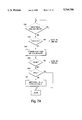
- control logic 130 determines in step 302 whether the corresponding pixel is presently in Z cache 110. This determination is made by comparing the new Z address with the addresses of each of the ID fields 152 (FIG. 5) of Z cache 110. When one of the cache ID fields matches the new Z address, a cache hit occurs.
- each cache entry contains a tile of four bytes corresponding to four different pixels, the two low order bits of the addresses are not compared. One of the four bytes is selected in the comparator using the two low order bits of the new Z address.
- the H byte of the new Z value is compared with the H byte of the corresponding cache entry in step 304. Step 304 is performed by the H byte comparator 122.
- the two low order bits of the new Z address are used to generate the select signal for multiplexer 210 to thereby select the appropriate byte from the addressed cache tile.
- step 306 the equal-to comparator 220 of H byte comparator 122 determines whether the H byte of the new Z value is equal to the H byte of the cache Z value.
- step 308 the greater-than comparator 222 of H byte comparator 122 determines whether the H byte of the new Z value is greater than the H byte of the cache Z value.
- the condition wherein the byte of the new Z value is less than the byte of the current Z value is designated as a pass. When a pass occurs, indicating that the new Z value is closer to the observer than the current Z value, the H, M and L bytes of the new Z value are written into the corresponding entry in the Z cache 110, in step 310.
- control logic 130 determines whether a cache hit occurs for the M byte of the new Z value.
- Step 320 requires comparison of the new Z address with the cache addresses and further requires examination of the read valid and update status bits.
- the read valid bit for the addressed cache entry is tested to determine if the M byte has been read into the Z cache 110 from the Z buffer memory 106.
- the Z cache 110 may include a valid M byte if the update bit is set, even if the read valid bit is not set.
- a cache hit occurs for the M byte if the read valid bit or the update bit is set for the addressed cache entry.
- the M byte of the new Z value is compared with the M byte of the cache Z value in step 322.
- the comparison of M bytes is performed by the M byte comparator 124 in the manner described above in connection with step 304.
- the equal-to comparator 220 of M byte comparator 124 determines whether the new and current M bytes are equal.
- the greater-than comparator 222 of M byte comparator 126 determines whether the M byte of the new Z value is greater than the M byte of the cache Z value.
- the M byte of the new Z value passes the comparison, the M and L bytes of the new Z value are written to the corresponding cache entry in step 328.
- the new Z value is discarded.
- step 340 the control logic 130 determines whether a cache hit occurs for the L byte of the new Z value in the manner described above in connection with step 320. In the case of a cache hit on the L byte in step 340, the L byte of the new Z value is compared with the L byte of the cache Z value in step 342. The comparison is performed by the L byte comparator 126 in the manner described above in connection with step 304.
- step 344 the equal-to comparator 220 of L byte comparator 126 determines whether the new and current L bytes are equal.
- step 346 the greater-than comparator 222 of L byte comparator 126 determines whether the L byte of the new Z value is greater than the L byte of the cache Z value.
- the L byte of the new Z value passes the comparison, the L byte of the new Z value is written into the corresponding cache entry in step 348.
- the new Z value is discarded.
- the new and current Z values are equal on all bytes, and the new Z value is processed according to a predetermined update criteria in step 350.
- the update criteria depends on the application.
- the new Z value replaces the current Z value when the new Z value is less than the current Z value.
- that criteria is not satisfied, and the new Z value is discarded.
- the new Z value replaces the current Z value when the new Z value is equal to or less than the current Z value.
- the new Z value replaces the current Z value.
- the process proceeds to FIG. 7D. Since the current Z value is not present in the Z cache 110, the Z value for the pixel corresponding to the new Z value is read from the Z buffer memory 106 in step 360. In particular, the four H bytes of a tile corresponding to the new Z value are read from the Z buffer memory. As indicated above, the tile may have a 2 ⁇ 2 pixel configuration or a 4 ⁇ 1 pixel configuration. The four H bytes from the Z buffer memory are supplied to the H byte comparator 122. The comparator 122 selects one of the four H bytes from memory and compares the H byte of the new Z value with the selected H byte from memory in step 362. With reference to FIG.
- the four H bytes from memory are input to the ZBUF inputs of multiplexers 202, 204, 206 and 208, respectively.
- the ZBUF inputs are selected, and the four H bytes are input to multiplexer 210.
- the two low order bits of the new Z address are used to generate a select signal for multiplexer 210.
- Multiplexer 210 selects the H byte corresponding to the pixel location of the new Z value.
- the selected H byte is supplied to comparators 220 and 222 for comparison with the H byte of the new Z value contained in register 200.
- the equal-to comparator 220 of H byte comparator 122 determines if the H byte of the new Z value is equal to the selected H byte from memory.
- step 366 the greater-than comparator 222 of H byte comparator 122 determines if the H byte of the new Z value is greater-than the selected H byte from memory.
- the H byte of the new Z value passes the comparison in step 366, the H, M and L bytes of the new Z value are written to the Z cache 110 in step 368.
- the three other H bytes read from the Z buffer memory in step 360 but not selected in step 362 are written to the corresponding cache entry in the H byte cache 112 in step 368.
- the cache entry selected for writing in step 368 is an empty cache entry if the Z cache 110 is not full. If the Z cache 110 is full, an entry is selected based on the age field.
- the new data is written into the cache entry with the highest value in the age field. Before new data is written into the cache entry, any bytes having the write valid bit true are written back to the Z buffer memory.
- the H byte of the new Z value does not pass the comparison in step 366, the four H bytes read from memory in step 360 are written into the Z cache 110 in step 370.
- a cache entry for writing the four H bytes is selected as described above in connection with step 368.
- step 380 the four M bytes of the tile corresponding to the new Z address are read from memory.
- step 382 the M byte of the new Z value is compared with a selected M byte of the four M bytes that were read from memory in step 380.
- the M byte selection and comparison operates in the manner described above in connection with the H byte comparison in step 362, except that the M byte comparator performs the selection and comparison.
- step 384 the equal to comparator 220 of M byte comparator 124 determines whether the M byte of the new Z value is equal to the selected M byte from memory.
- step 386 the greater than comparator 222 of M byte comparator 124 determines whether the M byte of the new Z value is greater than the selected M byte from memory.
- the M byte of the new Z value passes the comparison in step 386, the M and L bytes of the new Z value are written to the Z cache 110 in step 388.
- the three other M bytes that were read from memory in step 380 but not selected in step 382 are written to the other three byte locations in the same cache entry in step 388.
- the cache entry for writing of data in step 388 is selected as described above in connection with step 368.
- step 386 If the M byte of the new Z value does not pass the comparison in step 386, the four M bytes read from memory in step 380 are written into the Z cache 110 in step 390.
- the cache entry for writing in step 390 is selected as described above in connection with step 368.
- step 400 the four L bytes in the tile corresponding to the new Z address are read from memory.
- the L byte of the new Z value is compared with a selected one of the four L bytes from memory in step 402.
- the two low order bits of the new Z address are used to select one of the four L bytes from memory.
- the comparison of L bytes is performed by the L byte comparator 126 as described above in connection with step 362.
- step 404 the equal-to comparator 220 of L byte comparator 126 determines if the L byte of the new Z value is equal to the selected L byte from memory.
- step 406 the greater-than comparator 222 of L byte comparator 126 determines whether the L byte of the new Z value is greater than the selected L byte from memory.
- the L byte of the new Z value passes the comparison in step 406
- the L byte of the new Z value is written to the Z cache 110 in step 408.
- the three other L bytes read from memory in step 400 but not selected in step 402 are written into the same cache entry in step 408.
- the cache entry for writing in step 408 is selected as described above in connection with step 368.
- the L byte of the new Z value does not pass the comparison in step 406, the four L bytes read from memory in step 400 are written into the Z cache 110 in step 410.
- the cache entry for writing in step 410 is selected as described above in connection with step 368.
- the new and current Z values are equal, and the new Z value is processed according to a predetermined criteria in step 412.
- the processing in step 412 can be the same as described above in connection with step 350.
- each cache entry in Z cache 110 and the corresponding status bits contains H, M and L bytes for a tile of four pixels.
- the cache entry includes Z values Za, Zb, Zc and Zd.
- the h, m and I indicate data read from the Z buffer memory, while the H, M and L indicate new Z data updated from the pixel generator.
- the associated read valid field 158, write valid field 160 and update field 162 are shown. Bits in the read valid field are set when Z data is loaded from the Z buffer memory. Bits in the write valid field are set when the data is loaded from the pixel generator. When one of the Z values in the cache is updated by the pixel generator, the corresponding bit is set in the update field.
- the H and M bytes have been read from memory and stored in the cache as shown by the read valid bits.
- the write valid field indicates that when this cache entry is flushed, all bytes must be written to the Z buffer memory.
- the update field shows that the values Za and Zc have been modified. This information is necessary in case the L byte is needed to resolve the comparison for Zb or Zd. When the L byte is read, the L bytes for Za and Zc will not be updated from the Z buffer memory since the data in the cache is newer than the Z buffer data.
- the tile configuration in the Z cache 110 is preferably programmable. This permits the tile configuration to be optimized for the graphics primitive being processed.
- a 2 ⁇ 2 tile configuration or a 4 ⁇ 1 configuration is utilized.
- the 2 ⁇ 2 tile configuration is illustrated in FIG. 9A
- the 4 ⁇ 1 tile configuration is illustrated in FIG. 9B.
- pixels a and b are located on one scan line of the display screen
- pixels c and d are located on the next scan line of the display screen.
- Pixels a and b are located above pixels c and d, respectively.
- pixels a, b, c and d are located along a single scan line.
- pixels c and d are separated from pixels a and b by two pixels because dual interleaved memory controllers are utilized. It will be understood that the pixels in the 4 ⁇ 1 tile configuration may be separated by more or fewer pixels than illustrated in FIG. 9B, or may be consecutive, depending on the configuration of the memory controller.
- the 2 ⁇ 2 tile configuration is utilized for primitives having a relatively small dimension along the scan line, whereas the 4 ⁇ 1 tile configuration is utilized for primitives having a relatively large dimension along the scan line.
- the dimension of the primitive is determined in the pixel generator 100 (FIG. 3), and a control signal (long mode) is provided to the Z value processor 102.
- the 4 ⁇ 1 tile configuration is selected for primitives having a dimension of more than 128 pixels along the scan line. It will be understood that different criteria can be utilized for selecting different tile configurations. Furthermore, a variety of different tile configurations may be utilized and more than two tile configurations may be made available for selection.
- the circuitry shown and described herein is given by way of example only.
- the circuitry is preferably implemented in a large scale custom integrated circuit using logic synthesis software that is commercially available, for example, from Synopsys.
- the logic synthesis software optimizes and translates circuit descriptions written in high level languages, such as Verilog, into logic gates.
- the circuitry may be implemented using a CMOS process that produces 1 micron FET's which operate at 5 volts, a CMOS process that produces 0.6 micron drawn gate length devices which operate at 3.3 volts, or any other suitable process for implementing digital circuits.
Abstract
Description
Claims (15)
Priority Applications (1)
| Application Number | Priority Date | Filing Date | Title |
|---|---|---|---|
| US08/594,191 US5760780A (en) | 1996-01-31 | 1996-01-31 | Computer graphics system using caching of pixel Z values to improve rendering performance |
Applications Claiming Priority (1)
| Application Number | Priority Date | Filing Date | Title |
|---|---|---|---|
| US08/594,191 US5760780A (en) | 1996-01-31 | 1996-01-31 | Computer graphics system using caching of pixel Z values to improve rendering performance |
Publications (1)
| Publication Number | Publication Date |
|---|---|
| US5760780A true US5760780A (en) | 1998-06-02 |
Family
ID=24377901
Family Applications (1)
| Application Number | Title | Priority Date | Filing Date |
|---|---|---|---|
| US08/594,191 Expired - Lifetime US5760780A (en) | 1996-01-31 | 1996-01-31 | Computer graphics system using caching of pixel Z values to improve rendering performance |
Country Status (1)
| Country | Link |
|---|---|
| US (1) | US5760780A (en) |
Cited By (27)
| Publication number | Priority date | Publication date | Assignee | Title |
|---|---|---|---|---|
| US5995107A (en) * | 1996-08-02 | 1999-11-30 | Autodesk, Inc. | Caching in a three dimensional modeling and animation system |
| US6031550A (en) * | 1997-11-12 | 2000-02-29 | Cirrus Logic, Inc. | Pixel data X striping in a graphics processor |
| US6166743A (en) * | 1997-03-19 | 2000-12-26 | Silicon Magic Corporation | Method and system for improved z-test during image rendering |
| US6222552B1 (en) * | 1996-07-26 | 2001-04-24 | International Business Machines Corporation | Systems and methods for caching depth information of three-dimensional images |
| US6271851B1 (en) * | 1999-07-26 | 2001-08-07 | Silicon Integrated Systems Corporation | Z-buffer pre-test for 3D graphic performance enhancement |
| US6449328B1 (en) | 2000-05-15 | 2002-09-10 | International Business Machines Corporation | Method and apparatus for shifting data from registers |
| US6492987B1 (en) * | 1998-08-27 | 2002-12-10 | Ati Technologies, Inc. | Method and apparatus for processing object elements that are being rendered |
| US20030001861A1 (en) * | 2000-01-10 | 2003-01-02 | Watson David W. | Method and apparatus for pixel filtering using shared filter resource between overlay and texture mapping engines |
| WO2003058558A1 (en) * | 2001-12-31 | 2003-07-17 | Intel Corporation | Depth write disable for zone rendering |
| US6720964B1 (en) | 1998-08-27 | 2004-04-13 | Ati International Srl | Method and apparatus for processing portions of primitives that are being rendered |
| US20040111561A1 (en) * | 1998-10-23 | 2004-06-10 | Klein Dean A. | System and method for managing a cache memory |
| US6804411B1 (en) | 2000-05-15 | 2004-10-12 | International Business Machines Corporation | Method, system, and program for decompressing and aligning line work data from multiple objects |
| US6850338B1 (en) | 2000-05-12 | 2005-02-01 | International Business Machines Corporation | Method, system, program, and data structure for generating raster objects |
| US6894796B1 (en) | 2000-05-12 | 2005-05-17 | International Business Machines Corporation | Method, system, and logic for selecting line work and control data for a pixel from multiple objects of line work data provided for the pixel |
| US6961134B1 (en) | 2000-05-15 | 2005-11-01 | International Business Machines Corporation | Method, system, and logic using multiplexers to select data for pixels from multiple objects |
| US20070006065A1 (en) * | 2005-07-01 | 2007-01-04 | Microsoft Corporation | Conditional event timing for interactive multimedia presentations |
| US20070006062A1 (en) * | 2005-07-01 | 2007-01-04 | Microsoft Corporation | Synchronization aspects of interactive multimedia presentation management |
| US20070005758A1 (en) * | 2005-07-01 | 2007-01-04 | Microsoft Corporation | Application security in an interactive media environment |
| US20070006063A1 (en) * | 2005-07-01 | 2007-01-04 | Microsoft Corporation | Synchronization aspects of interactive multimedia presentation management |
| US20070005757A1 (en) * | 2005-07-01 | 2007-01-04 | Microsoft Corporation | Distributing input events to multiple applications in an interactive media environment |
| US20070046681A1 (en) * | 2005-08-23 | 2007-03-01 | Canon Kabushiki Kaisha | Memory apparatus and memory control method |
| WO2007005327A3 (en) * | 2005-07-01 | 2007-06-21 | Microsoft Corp | Rendering and compositing multiple applications in an interactive media environment |
| US7394568B1 (en) | 2000-05-15 | 2008-07-01 | Infoprint Solutions Company Llc | Method, system, and logic for selecting pixel data from multiple objects |
| US7721308B2 (en) | 2005-07-01 | 2010-05-18 | Microsoft Corproation | Synchronization aspects of interactive multimedia presentation management |
| US20100194747A1 (en) * | 2009-02-02 | 2010-08-05 | Microsoft Corporation | Dynamic Fragment Coverage Antialiasing |
| US8020084B2 (en) | 2005-07-01 | 2011-09-13 | Microsoft Corporation | Synchronization aspects of interactive multimedia presentation management |
| US8656268B2 (en) | 2005-07-01 | 2014-02-18 | Microsoft Corporation | Queueing events in an interactive media environment |
Citations (2)
| Publication number | Priority date | Publication date | Assignee | Title |
|---|---|---|---|---|
| US4965751A (en) * | 1987-08-18 | 1990-10-23 | Hewlett-Packard Company | Graphics system with programmable tile size and multiplexed pixel data and partial pixel addresses based on tile size |
| US5301263A (en) * | 1990-09-18 | 1994-04-05 | Hewlett-Packard Company | High memory bandwidth system for updating z-buffer values |
-
1996
- 1996-01-31 US US08/594,191 patent/US5760780A/en not_active Expired - Lifetime
Patent Citations (2)
| Publication number | Priority date | Publication date | Assignee | Title |
|---|---|---|---|---|
| US4965751A (en) * | 1987-08-18 | 1990-10-23 | Hewlett-Packard Company | Graphics system with programmable tile size and multiplexed pixel data and partial pixel addresses based on tile size |
| US5301263A (en) * | 1990-09-18 | 1994-04-05 | Hewlett-Packard Company | High memory bandwidth system for updating z-buffer values |
Cited By (49)
| Publication number | Priority date | Publication date | Assignee | Title |
|---|---|---|---|---|
| US6222552B1 (en) * | 1996-07-26 | 2001-04-24 | International Business Machines Corporation | Systems and methods for caching depth information of three-dimensional images |
| US5995107A (en) * | 1996-08-02 | 1999-11-30 | Autodesk, Inc. | Caching in a three dimensional modeling and animation system |
| US6166743A (en) * | 1997-03-19 | 2000-12-26 | Silicon Magic Corporation | Method and system for improved z-test during image rendering |
| US6031550A (en) * | 1997-11-12 | 2000-02-29 | Cirrus Logic, Inc. | Pixel data X striping in a graphics processor |
| US6492987B1 (en) * | 1998-08-27 | 2002-12-10 | Ati Technologies, Inc. | Method and apparatus for processing object elements that are being rendered |
| US6720964B1 (en) | 1998-08-27 | 2004-04-13 | Ati International Srl | Method and apparatus for processing portions of primitives that are being rendered |
| US20040111588A1 (en) * | 1998-10-23 | 2004-06-10 | Klein Dean A. | System and method for managing a cache memory |
| US7257697B2 (en) | 1998-10-23 | 2007-08-14 | Micron Technology, Inc. | Processing system with general purpose execution unit and separate independently operating data string manipulation unit |
| US7165143B2 (en) | 1998-10-23 | 2007-01-16 | Micron Technology, Inc. | System and method for manipulating cache data |
| US7370150B2 (en) | 1998-10-23 | 2008-05-06 | Micron Technology, Inc. | System and method for managing a cache memory |
| US20040111561A1 (en) * | 1998-10-23 | 2004-06-10 | Klein Dean A. | System and method for managing a cache memory |
| US7093093B2 (en) | 1998-10-23 | 2006-08-15 | Micron Technology, Inc. | Cache management system |
| US20040111595A1 (en) * | 1998-10-23 | 2004-06-10 | Klein Dean A. | System and method for managing a cache memory |
| US20040123074A1 (en) * | 1998-10-23 | 2004-06-24 | Klein Dean A. | System and method for manipulating cache data |
| US7120744B2 (en) | 1998-10-23 | 2006-10-10 | Micron Technology, Inc. | System and method for managing a cache memory |
| US7103719B2 (en) * | 1998-10-23 | 2006-09-05 | Micron Technology, Inc. | System and method for managing a cache memory |
| US6271851B1 (en) * | 1999-07-26 | 2001-08-07 | Silicon Integrated Systems Corporation | Z-buffer pre-test for 3D graphic performance enhancement |
| US7158147B2 (en) * | 2000-01-10 | 2007-01-02 | Intel Corporation | Method and apparatus for pixel filtering using shared filter resource between overlay and texture mapping engines |
| US20030001861A1 (en) * | 2000-01-10 | 2003-01-02 | Watson David W. | Method and apparatus for pixel filtering using shared filter resource between overlay and texture mapping engines |
| US20070103487A1 (en) * | 2000-01-10 | 2007-05-10 | Intel Corporation | Pixel filtering using shared filter resource between overlay and texture mapping engines |
| US7439986B2 (en) | 2000-01-10 | 2008-10-21 | Intel Corporation | Pixel filtering using shared filter resource between overlay and texture mapping engines |
| US6894796B1 (en) | 2000-05-12 | 2005-05-17 | International Business Machines Corporation | Method, system, and logic for selecting line work and control data for a pixel from multiple objects of line work data provided for the pixel |
| US6850338B1 (en) | 2000-05-12 | 2005-02-01 | International Business Machines Corporation | Method, system, program, and data structure for generating raster objects |
| US7394568B1 (en) | 2000-05-15 | 2008-07-01 | Infoprint Solutions Company Llc | Method, system, and logic for selecting pixel data from multiple objects |
| US6804411B1 (en) | 2000-05-15 | 2004-10-12 | International Business Machines Corporation | Method, system, and program for decompressing and aligning line work data from multiple objects |
| US6961134B1 (en) | 2000-05-15 | 2005-11-01 | International Business Machines Corporation | Method, system, and logic using multiplexers to select data for pixels from multiple objects |
| US6449328B1 (en) | 2000-05-15 | 2002-09-10 | International Business Machines Corporation | Method and apparatus for shifting data from registers |
| US6747657B2 (en) | 2001-12-31 | 2004-06-08 | Intel Corporation | Depth write disable for zone rendering |
| US20040257373A1 (en) * | 2001-12-31 | 2004-12-23 | Doyle Peter L. | Depth write disable for zone rendering |
| US6954208B2 (en) | 2001-12-31 | 2005-10-11 | Intel Corporation | Depth write disable for rendering |
| WO2003058558A1 (en) * | 2001-12-31 | 2003-07-17 | Intel Corporation | Depth write disable for zone rendering |
| US20070006065A1 (en) * | 2005-07-01 | 2007-01-04 | Microsoft Corporation | Conditional event timing for interactive multimedia presentations |
| US7721308B2 (en) | 2005-07-01 | 2010-05-18 | Microsoft Corproation | Synchronization aspects of interactive multimedia presentation management |
| WO2007005327A3 (en) * | 2005-07-01 | 2007-06-21 | Microsoft Corp | Rendering and compositing multiple applications in an interactive media environment |
| US20070005757A1 (en) * | 2005-07-01 | 2007-01-04 | Microsoft Corporation | Distributing input events to multiple applications in an interactive media environment |
| US20070006063A1 (en) * | 2005-07-01 | 2007-01-04 | Microsoft Corporation | Synchronization aspects of interactive multimedia presentation management |
| US20070005758A1 (en) * | 2005-07-01 | 2007-01-04 | Microsoft Corporation | Application security in an interactive media environment |
| US20070006062A1 (en) * | 2005-07-01 | 2007-01-04 | Microsoft Corporation | Synchronization aspects of interactive multimedia presentation management |
| JP2009505170A (en) * | 2005-07-01 | 2009-02-05 | マイクロソフト コーポレーション | Rendering and compositing multiple applications in an interactive media environment |
| US8799757B2 (en) | 2005-07-01 | 2014-08-05 | Microsoft Corporation | Synchronization aspects of interactive multimedia presentation management |
| US8656268B2 (en) | 2005-07-01 | 2014-02-18 | Microsoft Corporation | Queueing events in an interactive media environment |
| US8305398B2 (en) | 2005-07-01 | 2012-11-06 | Microsoft Corporation | Rendering and compositing multiple applications in an interactive media environment |
| US7941522B2 (en) | 2005-07-01 | 2011-05-10 | Microsoft Corporation | Application security in an interactive media environment |
| US8020084B2 (en) | 2005-07-01 | 2011-09-13 | Microsoft Corporation | Synchronization aspects of interactive multimedia presentation management |
| US8108787B2 (en) | 2005-07-01 | 2012-01-31 | Microsoft Corporation | Distributing input events to multiple applications in an interactive media environment |
| US20070046681A1 (en) * | 2005-08-23 | 2007-03-01 | Canon Kabushiki Kaisha | Memory apparatus and memory control method |
| US7616210B2 (en) * | 2005-08-23 | 2009-11-10 | Canon Kabushiki Kaisha | Memory apparatus and memory control method |
| US20100194747A1 (en) * | 2009-02-02 | 2010-08-05 | Microsoft Corporation | Dynamic Fragment Coverage Antialiasing |
| US8686999B2 (en) * | 2009-02-02 | 2014-04-01 | Microsoft Corporation | Dynamic fragment coverage antialiasing |
Similar Documents
| Publication | Publication Date | Title |
|---|---|---|
| US5760780A (en) | Computer graphics system using caching of pixel Z values to improve rendering performance | |
| US5801711A (en) | Polyline and triangle strip data management techniques for enhancing performance of computer graphics system | |
| EP0747825B1 (en) | SDRAM data allocation system and method | |
| US5821950A (en) | Computer graphics system utilizing parallel processing for enhanced performance | |
| US5896136A (en) | Computer graphics system with improved blending | |
| US5751292A (en) | Texture mapping method and system | |
| EP0747858B1 (en) | Texture cache | |
| US5606650A (en) | Method and apparatus for storage and retrieval of a texture map in a graphics display system | |
| EP0747860B1 (en) | Texture mapping data storage allocation method and system | |
| EP0747857B1 (en) | 3D Bypass for download of textures | |
| US6141725A (en) | Updating a local memory based on information provided by a host computer | |
| US5982384A (en) | System and method for triangle rasterization with frame buffers interleaved in two dimensions | |
| US6819324B2 (en) | Memory interleaving technique for texture mapping in a graphics system | |
| US5920687A (en) | Z-buffer storage based on opacity and depth using pointers | |
| US5321809A (en) | Categorized pixel variable buffering and processing for a graphics system | |
| US5847717A (en) | Data synchronization between a plurality of asynchronous data renderers | |
| JPH08212382A (en) | Z-buffer tag memory constitution | |
| US20030038810A1 (en) | Predictive optimizer for dram memory | |
| US6812928B2 (en) | Performance texture mapping by combining requests for image data | |
| US5696944A (en) | Computer graphics system having double buffered vertex ram with granularity | |
| US6930684B2 (en) | Method and apparatus for accelerating occlusion culling in a graphics computer | |
| US5784075A (en) | Memory mapping techniques for enhancing performance of computer graphics system | |
| EP0747826B1 (en) | Cache system with simultaneous tag comparison | |
| US5732248A (en) | Multistep vector generation for multiple frame buffer controllers | |
| US7053902B1 (en) | Image processing apparatus and method of processing images that stops operation of pixel processing circuits when pixel data to be processed is not needed |
Legal Events
| Date | Code | Title | Description |
|---|---|---|---|
| AS | Assignment |
Owner name: HEWLETT-PACKARD COMPANY, CALIFORNIA Free format text: ASSIGNMENT OF ASSIGNORS INTEREST;ASSIGNORS:LARSON, RONALD D.;DOWDELL, CHARLES R.;REEL/FRAME:008011/0909 Effective date: 19960327 |
|
| STCF | Information on status: patent grant |
Free format text: PATENTED CASE |
|
| FEPP | Fee payment procedure |
Free format text: PAYOR NUMBER ASSIGNED (ORIGINAL EVENT CODE: ASPN); ENTITY STATUS OF PATENT OWNER: LARGE ENTITY |
|
| AS | Assignment |
Owner name: HEWLETT-PACKARD COMPANY, COLORADO Free format text: MERGER;ASSIGNOR:HEWLETT-PACKARD COMPANY;REEL/FRAME:011523/0469 Effective date: 19980520 |
|
| CC | Certificate of correction | ||
| FPAY | Fee payment |
Year of fee payment: 4 |
|
| FPAY | Fee payment |
Year of fee payment: 8 |
|
| FPAY | Fee payment |
Year of fee payment: 12 |
|
| AS | Assignment |
Owner name: HEWLETT-PACKARD DEVELOPMENT COMPANY, L.P., TEXAS Free format text: ASSIGNMENT OF ASSIGNORS INTEREST;ASSIGNOR:HEWLETT-PACKARD COMPANY;REEL/FRAME:026945/0699 Effective date: 20030131 |