US5744976A - Floating guide plate test fixture - Google Patents
Floating guide plate test fixture Download PDFInfo
- Publication number
- US5744976A US5744976A US08/653,189 US65318996A US5744976A US 5744976 A US5744976 A US 5744976A US 65318996 A US65318996 A US 65318996A US 5744976 A US5744976 A US 5744976A
- Authority
- US
- United States
- Prior art keywords
- test
- guide plate
- probes
- circuit board
- plate
- Prior art date
- Legal status (The legal status is an assumption and is not a legal conclusion. Google has not performed a legal analysis and makes no representation as to the accuracy of the status listed.)
- Expired - Lifetime
Links
Images


Classifications
-
- G—PHYSICS
- G01—MEASURING; TESTING
- G01R—MEASURING ELECTRIC VARIABLES; MEASURING MAGNETIC VARIABLES
- G01R1/00—Details of instruments or arrangements of the types included in groups G01R5/00 - G01R13/00 and G01R31/00
- G01R1/02—General constructional details
- G01R1/06—Measuring leads; Measuring probes
- G01R1/067—Measuring probes
- G01R1/06705—Apparatus for holding or moving single probes
Definitions
- the present invention generally relates to test fixtures for circuit boards and, more particularly, to automated test fixtures for aligning undersized test points on a circuit board with test probes.
- circuit board designers are constantly faced with the challenge of packaging more and more electronics into a smaller amount of space. Often, there is little that can be done concerning the size or number of components required for a given function. Hence, where possible, other physical attributes of the circuit board design, such as the test points, are often minimized or eliminated.
- Test points are necessary on circuit boards to allow interconnection to test equipment via a test fixture.
- a test fixture is typically an automated device which comprises a plurality of fixed upwardly projecting test probes. Each of the test probes correspond to a test point on the circuit board such that when the board is pulled down on top of the probes, each probe is brought into electrical contact with its corresponding test point.
- test points are sometimes omitted for portions of a given board design or, alternatively, if test points are provided they may be of a diameter too small for the fixture to contact reliably. Omitted test points result in portions of the board going untested and thereby jeopardizing product quality. Similarly, if the test points are too small to reliably contact the test probes, manufacturing costs are increased due to retest cycles and delays.
- FIG. 1 shows an example of a test fixture for testing circuit boards generally referred to by the reference numeral 10.
- the test fixture 10 comprises a probe plate 12 having a plurality of upwardly projecting test probes 14. Each of the test probes 14 correspond to a test point 16 on the circuit board under test 18.
- the circuit board 18 sits on blocks 20 above a rigid guide plate 22.
- the guide plate 22 must be made of a non-conductive material so as not to interfere with the electrical probes 14.
- a vacuum chamber 28 defined by a vacuum mat 30 and vacuum seal 32
- atmospheric pressure pushes down on the vacuum mat 30 compressing springs 26 and causing the guide plate 22 to move in a downward direction along guide pin 34.
- a backer plate 36 connected to the guide plate 22, pushes down on backer post 38 which, in turn, pushes down on the circuit board 18 under test.
- Guide apertures 40 allow probe tips 42 to slide therethrough and make electrical contact with the test points 16.
- the total alignment error for the text fixture is the aggregate of all alignment errors introduced at the various alignment points of the individual fixture parts. This necessitates the need for relatively large guide apertures 40.
- the summation of these and other alignment tolerances yields a probe-center to test-point-center misalignment of 0.017" to 0.027" (0.43 to 0.69 mm). Therefore, the diameter of the test points designed onto the circuit board must be at least twice these values to ensure proper electrical contact (i.e., 0.034" to 0.054" or 0.86 to 1.37 mm).
- a guided probe test fixture may be used as shown in FIG. 2.
- the basic fixture assembly is the same as that shown in FIG. 1. Accordingly, like elements are labeled the same.
- the rigid guide plate 22 has affixed thereto a funnel plate 23.
- the funnel plate 23 has apertures 40' which are smaller in diameter than the apertures 40 in the guide plate 23 and thereby bias the probe tips 42 to establish a closer dimensional relationship to the target test points 16.
- Test point diameters as small as 0.025" (0.64 mm) are achievable; however, most of the misalignment tolerances for the standard fixture still apply.
- the funnel plate 23 may be made of nylon or similar reduced-friction polymer materials to minimize binding. However, the probe tips 42 still occasionally rub or drag on the funnel plate 23 causing binding which, in turn, results in a degradation in contact force.
- FIG. 3 shows a split probe fixture which provides even greater accuracy.
- the probes 14 are split at the tips 42.
- Small piston-type probes 43 are installed directly into the guide plate apertures 40.
- This split probe design serves to further reduce the misalignment tolerances between the probes 43 and test points 16 since a lessor number of component errors are involved. For example, the errors in the probe plate no longer contribute to the misalignment since the probe plate is unrelated to the piston-type probes and the probe points.
- a vacuum actuated test fixture for testing circuit boards includes a plurality of upwardly projecting test probes.
- a circuit board to be tested includes a plurality of test points to be contacted by a corresponding test probe.
- the circuit to be tested is fixed to a floating guide plate having apertures therethrough aligned with the test points. As the floating guide plate is lowered over the test probes the guide plate is permitted to float in a lateral direction to achieve proper alignment between the probes and the apertures. Once aligned, the probes continue to pass through the apertures to make contact with their respective test points.
- a card tooling pin is provided which securely aligns the circuit board under test to the floating guide plate. The tooling pin also establishes loose alignment of the floating plate with respect to the probes during floating plate installation.
- FIG. 1 is a diagram showing a related test fixture for aligning test probes to test points on a circuit board
- FIG. 2 is a diagram showing a related guided probe test fixture for aligning test probes to test points on a circuit board
- FIG. 3 is a diagram showing a related split probe test fixture for aligning test probes to test points on a circuit board
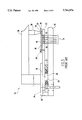
- FIG. 4 is a diagram showing a floating guide plate test probe fixture according to the present invention.
- the test fixture 11 comprises a probe plate 12 having a field of upwardly projecting test probes 14. Each of the test probes 14 correspond to a testpoint 16 on the circuit board 18 under test.
- the test fixture of the present invention includes a floating guide plate 50 onto which the circuit board under test 18 is secured atop of blocks 50.
- the floating guide plate 21 floats on return springs 52 and 54 and is captured by vacuum chamber plate upper lip 66.
- a press fit card tooling pin 56 securely aligns test points 16 with guide plate apertures 40.
- the pin 56 also establishes loose alignment between the floating plate 50 and the probe plate 12.
- the pin 56 fits relatively loosely in pin aperture 58 to permit the floating guide plate 50 to float. Additionally, this relaxed fit 58 helps avoid undue stress to the probes 14 from any transverse loading that may be experienced during pull-down since the total amount offloat is limited by the fit.
- the floating guide plate 50 establishes a dimensional relationship betweenthe probe field 14 and the board 18 under test to achieve a total possible misalignment of only 0.008 to 0.012 inches (0.2 to 0.3 mm), thus permitting the probes to reliably contact undersized test points. Note that the resulting tolerance is equivalent to the split probe fixture shown in FIG. 3; however, the present invention has the advantage of usingstandard probes thereby reducing initial cost as well as maintenance costs.
- the floating guide plate 50 is preferably constructed of a low friction polymer to help prevent binding, similar to the guide plate of a guided probe fixture shown in FIG. 2.
- lower cost is possible since the floating plate 50 simply rests on top of support springs, 52 and 54, rather than being aligned and fixedly assembled to a top plate as with a guided probe fixture.
- the floating guide plate 50 of the present invention moves laterally during a pull-down.
- funnel shaped apertures 40 may be used having smaller through openings at the probe emerging end thus further increasing pointing accuracy.
- a vacuum chamber plate 60 performs the primary function of applying force to the circuit board under test 18 for contact with the probes 14.
- the vacuum mat 30 and vacuum chamber plate 60 translate downward from atmospheric pressure along guide pin 34.
- a hinged backer gate arm 36 moves with the vacuum chamber plate 60and transfers force to the circuit board 18 with backer posts 38 compressing spring 54.
- the vacuum chamber plate 60 has an upper lip 66 which pushes down on a lower lip 68 of the floating guide plate 50 thus compressing spring 52.
- Spaces 62 are left to allow the lowerlip 68 of the guide plate 50 to slip under the upper lip 66 to permit limited lateral movement of the floating guide plate 50 during a pull-downoperation.
- the vacuum chamber plate 60 and the floating guide plate 50 are not continuous, overall strength or resistance to flexure is reduced. However, non-conductivity is no longer a requirement for the chamber plate 60 since it does not contact the probes. Hence, the chamber plate 60 may be constructed of materials stronger than standard fixture plates such as structural aluminum or steel.
- a testing device 64 such as a programmable signal generator or meter, may be connected to the probes 14. Once the circuit board 18 is pulled down, test signals are supplied through selected probesto the test points 16 on the board 18, while other probes read the resultant signals at other test points 16. In this manner, the integrity of the circuit board can be automatically tested.
Abstract
Description
Claims (15)
Priority Applications (1)
| Application Number | Priority Date | Filing Date | Title |
|---|---|---|---|
| US08/653,189 US5744976A (en) | 1996-05-24 | 1996-05-24 | Floating guide plate test fixture |
Applications Claiming Priority (1)
| Application Number | Priority Date | Filing Date | Title |
|---|---|---|---|
| US08/653,189 US5744976A (en) | 1996-05-24 | 1996-05-24 | Floating guide plate test fixture |
Publications (1)
| Publication Number | Publication Date |
|---|---|
| US5744976A true US5744976A (en) | 1998-04-28 |
Family
ID=24619854
Family Applications (1)
| Application Number | Title | Priority Date | Filing Date |
|---|---|---|---|
| US08/653,189 Expired - Lifetime US5744976A (en) | 1996-05-24 | 1996-05-24 | Floating guide plate test fixture |
Country Status (1)
| Country | Link |
|---|---|
| US (1) | US5744976A (en) |
Cited By (1)
| Publication number | Priority date | Publication date | Assignee | Title |
|---|---|---|---|---|
| US20100071948A1 (en) * | 2008-09-19 | 2010-03-25 | Hon Hai Precision Industry Co., Ltd. | Printed circuit board and method of manufacturing the same |
Citations (13)
| Publication number | Priority date | Publication date | Assignee | Title |
|---|---|---|---|---|
| US4061969A (en) * | 1975-05-17 | 1977-12-06 | International Computers Limited | Apparatus for testing printed circuit boards |
| US4115735A (en) * | 1976-10-14 | 1978-09-19 | Faultfinders, Inc. | Test fixture employing plural platens for advancing some or all of the probes of the test fixture |
| US4538104A (en) * | 1983-04-11 | 1985-08-27 | Test Point 1, Inc. | In-circuit test apparatus for printed circuit board |
| US4626776A (en) * | 1984-06-07 | 1986-12-02 | O. B. Test Group, Inc. | Programmable test fixture |
| US4746861A (en) * | 1986-08-21 | 1988-05-24 | Tti Testron, Inc. | Test fixture for printed circuit board assembly |
| US4771234A (en) * | 1986-11-20 | 1988-09-13 | Hewlett-Packard Company | Vacuum actuated test fixture |
| US4783624A (en) * | 1986-04-14 | 1988-11-08 | Interconnect Devices, Inc. | Contact probe devices and method |
| US4870354A (en) * | 1988-08-11 | 1989-09-26 | Zehntel, Inc. | Apparatus for contacting a printed circuit board with an array of test probes |
| US4935696A (en) * | 1987-04-16 | 1990-06-19 | Teradyne, Inc. | Test pin assembly for circuit board tester |
| US4935695A (en) * | 1988-07-13 | 1990-06-19 | Hewlett-Packard Company | Board alignment system |
| US5325052A (en) * | 1990-11-30 | 1994-06-28 | Tokyo Electron Yamanashi Limited | Probe apparatus |
| US5416428A (en) * | 1993-02-09 | 1995-05-16 | Everett Charles Technologies, Inc. | Marker probe |
| US5534787A (en) * | 1994-12-09 | 1996-07-09 | Vlsi Technology, Inc. | High-frequency coaxial interface test fixture |
-
1996
- 1996-05-24 US US08/653,189 patent/US5744976A/en not_active Expired - Lifetime
Patent Citations (13)
| Publication number | Priority date | Publication date | Assignee | Title |
|---|---|---|---|---|
| US4061969A (en) * | 1975-05-17 | 1977-12-06 | International Computers Limited | Apparatus for testing printed circuit boards |
| US4115735A (en) * | 1976-10-14 | 1978-09-19 | Faultfinders, Inc. | Test fixture employing plural platens for advancing some or all of the probes of the test fixture |
| US4538104A (en) * | 1983-04-11 | 1985-08-27 | Test Point 1, Inc. | In-circuit test apparatus for printed circuit board |
| US4626776A (en) * | 1984-06-07 | 1986-12-02 | O. B. Test Group, Inc. | Programmable test fixture |
| US4783624A (en) * | 1986-04-14 | 1988-11-08 | Interconnect Devices, Inc. | Contact probe devices and method |
| US4746861A (en) * | 1986-08-21 | 1988-05-24 | Tti Testron, Inc. | Test fixture for printed circuit board assembly |
| US4771234A (en) * | 1986-11-20 | 1988-09-13 | Hewlett-Packard Company | Vacuum actuated test fixture |
| US4935696A (en) * | 1987-04-16 | 1990-06-19 | Teradyne, Inc. | Test pin assembly for circuit board tester |
| US4935695A (en) * | 1988-07-13 | 1990-06-19 | Hewlett-Packard Company | Board alignment system |
| US4870354A (en) * | 1988-08-11 | 1989-09-26 | Zehntel, Inc. | Apparatus for contacting a printed circuit board with an array of test probes |
| US5325052A (en) * | 1990-11-30 | 1994-06-28 | Tokyo Electron Yamanashi Limited | Probe apparatus |
| US5416428A (en) * | 1993-02-09 | 1995-05-16 | Everett Charles Technologies, Inc. | Marker probe |
| US5534787A (en) * | 1994-12-09 | 1996-07-09 | Vlsi Technology, Inc. | High-frequency coaxial interface test fixture |
Cited By (1)
| Publication number | Priority date | Publication date | Assignee | Title |
|---|---|---|---|---|
| US20100071948A1 (en) * | 2008-09-19 | 2010-03-25 | Hon Hai Precision Industry Co., Ltd. | Printed circuit board and method of manufacturing the same |
Similar Documents
| Publication | Publication Date | Title |
|---|---|---|
| US3806801A (en) | Probe contactor having buckling beam probes | |
| US4665360A (en) | Docking apparatus | |
| US6066957A (en) | Floating spring probe wireless test fixture | |
| EP0840131B1 (en) | Loaded-board guided-probe test fixture | |
| US5818248A (en) | Loaded board test fixture with integral translator fixture for testing closely spaced test sites | |
| US6802720B2 (en) | Pin-array, separable, compliant electrical contact member | |
| US6064218A (en) | Peripherally leaded package test contactor | |
| US5663655A (en) | ESD protection for universal grid type test fixtures | |
| US5754057A (en) | Contact mechanism for test head of semiconductor test system | |
| EP0840130B1 (en) | Standard- and limited-access hybrid test fixture | |
| EP0360396A2 (en) | Force delivery system for improved precision membrane probe | |
| CN102656468B (en) | For the wiring plate tested loading printed circuit board (PCB) | |
| KR101284400B1 (en) | Zero insertion force printed circuit assembly connector system and method | |
| US6130547A (en) | Test apparatus for printed circuit board and assembly kit therefor | |
| US20080186037A1 (en) | Probe card and structure for fixing needle thereof | |
| US6169412B1 (en) | Adjustable tooling pin for a card test fixture | |
| JPS62182678A (en) | Test sight system | |
| US6794887B1 (en) | Test head including displaceable switch element | |
| US5744976A (en) | Floating guide plate test fixture | |
| KR20100069300A (en) | Probe card, and apparatus and method for testing semiconductor device | |
| US6885205B2 (en) | Test fixture assembly for printed circuit boards | |
| US6496001B1 (en) | System and method for probe mechanism planarization | |
| KR102193447B1 (en) | Test socket | |
| GB2145582A (en) | Electrical test probe assembly | |
| KR101540239B1 (en) | Probe Assembly and Probe Base Plate |
Legal Events
| Date | Code | Title | Description |
|---|---|---|---|
| AS | Assignment |
Owner name: INTERNATIONAL BUSINESS MACHINES CORPORATION, NEW Y Free format text: ASSIGNMENT OF ASSIGNORS INTEREST;ASSIGNORS:CAGGIANO, RAYMOND J.;HATLEY, JEFFREY A.;REEL/FRAME:008025/0773 Effective date: 19960521 |
|
| FEPP | Fee payment procedure |
Free format text: PAYOR NUMBER ASSIGNED (ORIGINAL EVENT CODE: ASPN); ENTITY STATUS OF PATENT OWNER: LARGE ENTITY |
|
| STCF | Information on status: patent grant |
Free format text: PATENTED CASE |
|
| FEPP | Fee payment procedure |
Free format text: PAYER NUMBER DE-ASSIGNED (ORIGINAL EVENT CODE: RMPN); ENTITY STATUS OF PATENT OWNER: LARGE ENTITY Free format text: PAYOR NUMBER ASSIGNED (ORIGINAL EVENT CODE: ASPN); ENTITY STATUS OF PATENT OWNER: LARGE ENTITY |
|
| FPAY | Fee payment |
Year of fee payment: 4 |
|
| FPAY | Fee payment |
Year of fee payment: 8 |
|
| FPAY | Fee payment |
Year of fee payment: 12 |
|
| AS | Assignment |
Owner name: GLOBALFOUNDRIES U.S. 2 LLC, NEW YORK Free format text: ASSIGNMENT OF ASSIGNORS INTEREST;ASSIGNOR:INTERNATIONAL BUSINESS MACHINES CORPORATION;REEL/FRAME:036550/0001 Effective date: 20150629 |
|
| AS | Assignment |
Owner name: GLOBALFOUNDRIES INC., CAYMAN ISLANDS Free format text: ASSIGNMENT OF ASSIGNORS INTEREST;ASSIGNORS:GLOBALFOUNDRIES U.S. 2 LLC;GLOBALFOUNDRIES U.S. INC.;REEL/FRAME:036779/0001 Effective date: 20150910 |
|
| AS | Assignment |
Owner name: GLOBALFOUNDRIES U.S. INC., NEW YORK Free format text: RELEASE BY SECURED PARTY;ASSIGNOR:WILMINGTON TRUST, NATIONAL ASSOCIATION;REEL/FRAME:056987/0001 Effective date: 20201117 |