US5737190A - Digital input/output circuit board - Google Patents
Digital input/output circuit board Download PDFInfo
- Publication number
- US5737190A US5737190A US08/521,182 US52118295A US5737190A US 5737190 A US5737190 A US 5737190A US 52118295 A US52118295 A US 52118295A US 5737190 A US5737190 A US 5737190A
- Authority
- US
- United States
- Prior art keywords
- input
- output
- module
- circuit board
- receptacles
- Prior art date
- Legal status (The legal status is an assumption and is not a legal conclusion. Google has not performed a legal analysis and makes no representation as to the accuracy of the status listed.)
- Expired - Lifetime
Links
Images


Classifications
-
- H—ELECTRICITY
- H05—ELECTRIC TECHNIQUES NOT OTHERWISE PROVIDED FOR
- H05K—PRINTED CIRCUITS; CASINGS OR CONSTRUCTIONAL DETAILS OF ELECTRIC APPARATUS; MANUFACTURE OF ASSEMBLAGES OF ELECTRICAL COMPONENTS
- H05K1/00—Printed circuits
- H05K1/02—Details
- H05K1/0286—Programmable, customizable or modifiable circuits
- H05K1/029—Programmable, customizable or modifiable circuits having a programmable lay-out, i.e. adapted for choosing between a few possibilities
-
- H—ELECTRICITY
- H05—ELECTRIC TECHNIQUES NOT OTHERWISE PROVIDED FOR
- H05K—PRINTED CIRCUITS; CASINGS OR CONSTRUCTIONAL DETAILS OF ELECTRIC APPARATUS; MANUFACTURE OF ASSEMBLAGES OF ELECTRICAL COMPONENTS
- H05K1/00—Printed circuits
- H05K1/02—Details
- H05K1/0296—Conductive pattern lay-out details not covered by sub groups H05K1/02 - H05K1/0295
- H05K1/0298—Multilayer circuits
-
- H—ELECTRICITY
- H05—ELECTRIC TECHNIQUES NOT OTHERWISE PROVIDED FOR
- H05K—PRINTED CIRCUITS; CASINGS OR CONSTRUCTIONAL DETAILS OF ELECTRIC APPARATUS; MANUFACTURE OF ASSEMBLAGES OF ELECTRICAL COMPONENTS
- H05K2201/00—Indexing scheme relating to printed circuits covered by H05K1/00
- H05K2201/10—Details of components or other objects attached to or integrated in a printed circuit board
- H05K2201/10007—Types of components
- H05K2201/10181—Fuse
-
- H—ELECTRICITY
- H05—ELECTRIC TECHNIQUES NOT OTHERWISE PROVIDED FOR
- H05K—PRINTED CIRCUITS; CASINGS OR CONSTRUCTIONAL DETAILS OF ELECTRIC APPARATUS; MANUFACTURE OF ASSEMBLAGES OF ELECTRICAL COMPONENTS
- H05K2201/00—Indexing scheme relating to printed circuits covered by H05K1/00
- H05K2201/10—Details of components or other objects attached to or integrated in a printed circuit board
- H05K2201/10227—Other objects, e.g. metallic pieces
- H05K2201/10325—Sockets, i.e. female type connectors comprising metallic connector elements integrated in, or bonded to a common dielectric support
Definitions
- the invention relates generally to the field of circuit boards and, more particularly, to a digital input/output circuit board.
- I/O Solid state input/output
- Such I/O systems enable a microprocessor or computer to receive input signals indicating the state of 120 volt switches via input modules, and to send output signals to activate external 120 volt devices via output modules.
- the known I/O systems enable microprocessors and computers to be utilized to control various devices in household and industrial settings.
- the known I/O systems typically include a base circuit board having a plurality of receptacles for mounting input and output modules, a connector for interfacing to a computer or microprocessor, a terminal strip for attaching field wires to field devices, and a fuse associated with each module.
- the base circuit boards conventionally have from one to thirty-two or more receptacles for mounting a selected number of modules. An input or an output module may be plugged into any given receptacle position on a circuit board.
- the known I/O circuit boards have a number of associated problems and disadvantages.
- the microprocessor or computer must have information as to whether a particular module position on the circuit board is occupied by an input or an output module. Accordingly, whenever the status of a module position changes, the microprocessor or computer information must be updated.
- the terminal strip must be wired for the proper configuration of each input or output module.
- Companies which manufacture large numbers of microprocessor or computer controlled equipment utilizing I/O module systems incur substantial labor costs related to the wiring of the terminal strips.
- I/O boards having a large number of modules require extensive wiring on the terminal strip to configure the modules.
- the terminal strip must be rewired in a time-consuming and tedious process.
- the present invention has been made in view of the above-described problems of the known I/O circuit boards and has as an object to provide a digital input/output circuit board which reduces manual wiring time and expenses.
- Another object of the present invention is to provide a digital I/O circuit board which provides flexibility of module selection and configuration.
- Yet another object of the present invention is to provide a digital I/O circuit board which complies with UL and CSA specifications.
- Still another object of the present invention is to provide a digital I/O circuit board which reduces reconfiguration time and expenses.
- the digital input/output circuit board in accordance with a preferred embodiment of the invention comprises a plurality of module receptacles for selectively mounting input modules or output modules.
- the module receptacles are electrically connectible to a computer.
- a plurality of wiring terminals are provided for attaching field wires to electrically connect the circuit board to field devices.
- the field devices may be devices from which an input signal is sent to the computer to indicate their state, or devices to which an output signal is sent from the computer to cause their activation.
- the circuit board further comprises a hot wiring terminal for attaching a hot power wire, and a neutral wiring terminal for attaching a neutral power wire.
- Means are further provided on the circuit board for selecting the status of each of the module receptacles as being either an input or an output, depending on the type of module mounted thereto.
- a method of connecting a computer and a digital I/O circuit board in accordance with the invention to field devices is also disclosed herein.
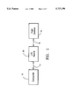
- FIG. 1 is an illustrational flow diagram of the general manner of use and operation of the I/O circuit board in accordance with the invention
- FIG. 2 is a top plan schematic view of a conventional I/O circuit board on which are mounted a plurality of input and output modules connected to field devices;
- FIG. 3 is a top plan schematic view of the conventional I/O circuit board of FIG. 2 with the modules mounted at reversed positions illustrating the labor intensive wiring changes required for reconfiguration;
- FIG. 4 is a top plan schematic view of an I/O circuit board in accordance with a preferred embodiment of the invention on which are mounted a plurality of input and output modules connected to field devices;
- FIG. 5 is a top plan schematic view of the I/O circuit board of FIG. 4 with the modules mounted at reversed positions;
- FIGS. 6A-6D are each top plan views illustrating the arrangement of the wiring connections and wiring of the four layers of the I/O circuit board in accordance with a preferred embodiment of the invention.
- FIG. 1 is a flow diagram of the general manner of use of a conventional I/O circuit board 20 and also the I/O circuit board in accordance with the present invention.
- the circuit board 20 is electrically connected to a computer 12 via a connector 14 and to one or more field devices 16 via field wiring 18.
- the computer receives input return signals from the field devices indicating their present state, and sends output signals to other field devices referred to herein as "loads" to activate these other devices.
- the input return signals may be received from electrical switches to indicate an "opened” or a "closed” state, or from other types of devices indicating their operating status as being either "on” or "off”.
- the output signals may be sent from the computer to loads including motors, solenoids, contactors and the like, to activate contacts and energize the devices.
- FIG. 2 schematically illustrates the electrical connection of the conventional I/O circuit board 20 to a pair of switches 22, 23 via field wiring 24, 25, and to a pair of loads 26, 27 via field wiring 28, 29.
- Input modules 30 and output modules 32 are shown removably mounted at spaced locations on the circuit board and being electrically connected to the field devices.
- the conventional circuit board may have as many as thirty-two locations for mounting modules, and an input or an output module may be mounted at any of the receptacle positions.
- the input modules 30 are electrically connected to a computer and to the switches 22, 23 to enable the computer to read the state (open or closed) of the switches, and the output modules 32 are electrically connected to the computer and to the loads 26, 27 to enable the computer to send output signals to selectively energize these devices. Any combination of input modules and output modules may be utilized on the circuit board depending on the number of switches or loads connected to the circuit board.
- the circuit board 20 further comprises a fuse 35 for each module 30, 32, and a screw terminal strip 34 having a pair of wiring terminals 36, 37 and 38, 39 for each of the modules 30, 32, respectively.
- the terminal strip is provided for electrically connecting the field wiring to the field switches 22, 23 and loads 26, 27.
- the terminal strip is wired for the proper configuration of an input or an output.
- field wires 24, 25 connect the respective switches 22, 23 to the terminals 36 associated with the input modules 30.
- the other terminal 37 for each input module is connected to a neutral power wire 42.
- field wires 28, 29 connect the respective loads 26, 27 to the terminals 39 associated with the output modules.
- the other terminal 38 for the output modules is connected to a hot power wire 40.
- FIG. 3 illustrates the conventional I/O circuit board of FIG. 2 electrically connected to the loads 26, 27 and switches 22, 23 arranged at reversed positions.
- the module arrangement of FIG. 3 is also reversed so that the input modules 30 are connected to the switches and the output modules 32 are connected to the loads.
- the reconfiguration of the modules requires significant rewiring of the terminal strip 34 so that the neutral power wire 42 is connected to the input modules 30 and the hot power wire 40 is connected to the output modules 32, and the field wires 24, 25, 28 and 29 are connected to the proper terminals on the terminal strip.
- FIG. 4 schematically depicts an I/O circuit board 50 in accordance with a preferred embodiment of the invention.
- the illustrated circuit board comprises two input modules 52 and two output modules 54 as in the conventional circuit board 20 depicted in FIG. 2.
- the circuit board may optionally have a different number of receptacles for mounting more than one module.
- the modules 52, 54 are removably mounted at receptacles (described in greater detail below) on the circuit board and are adapted to be electrically connected to a like number of field devices.
- the field devices may be loads and devices providing input signals such as switches.
- An input or an output module may be mounted at any of the receptacles, depending on the number and arrangement of the field devices.
- the circuit board 50 is electrically connected to a computer such as shown diagrammatically in FIG. 1 for the conventional I/O circuit board.
- a microprocessor (not shown) which is polled by the computer is preferably a component of the circuit board 50.
- the input modules 52 are electrically connected to the computer and to switches 56, 57 via field wiring 58, 59 to enable the computer to receive input signals to read the state of the switches, and the output modules 54 are also electrically connected to the computer and to loads 60, 61 via field wiring 62, 63 to enable the computer to send output signals to selectively activate the loads.
- the circuit board 50 integrates the hot and neutral wiring used to configure the input and output modules to reduce the amount of time and labor required to wire the terminal strip 64.
- a selecting device is incorporated as an element of the circuit board to provide flexibility and ease of reconfiguring the modules for different arrangements of field devices, and to reduce the number of terminals required for field wiring purposes.
- an insulated fuse 66 is provided for each of the input modules 52 and output modules 54 to function as the selecting device to enable selection for a given module position on the circuit board between an output or a input.
- the fuse is the preferred selecting device because it is a component of the circuit board wiring and also provides other advantages.
- the fuse is inexpensive and is an UL/CSA approved device. Being insulated, the fuse provides the safety advantage of eliminating shock hazards. Other types of UL/CSA approved devices such as switches and the like may optionally be used in the circuit board as the selecting device.
- the fuses 66 are each mounted at either an "input” or an "output” position on the circuit board, depending on whether the associated module is an input or an output module.
- the output modules 54 are connected to the loads 60, 61, and the fuses 66 are mounted at output positions as represented by solid lines.
- the input modules 52 are connected to the switches 56, 57, and the fuses 66 are mounted at input positions as also indicated by solid lines.
- the hot power wiring 68 and the neutral power wiring 70 are connected to the output modules 54 and the input modules 52, respectively.
- the circuit board 50 in accordance with the invention significantly reduces the number of wiring terminals associated with the terminal strip 64. Particularly, there is only one terminal 72 for each module 52, 54 and, additionally, two power terminals 74 for the hot wiring 68 and the neutral wiring 70. Thus, for the four modules there are a total of six terminals as compared to eight terminals in the conventional circuit board shown in FIGS. 2 and 3. For circuit boards having more modules, the reduction in the number of terminals as compared to the conventional circuit boards is even greater. For example, a circuit board in accordance with the invention having sixteen modules (not shown) requires eighteen terminals, while a conventional circuit board having sixteen modules (not shown) requires thirty-two terminals. The reduction in the number of terminals in the present circuit board provides significant time and cost advantages with respect to the reconfiguring of the circuit board for different combinations of field devices.
- FIG. 5 illustrates the circuit board of FIG. 4 electrically connected to the loads 60, 61 and switches 56, 57 arranged at reversed positions as compared to FIG. 4.
- the module arrangement of FIG. 5 is also reversed so that input modules 52 are connected to the switches 56, 57, and output modules 54 are connected to the loads 60, 61.
- the reconfiguration of the modules requires only the movement of the fuse 66 associated with each module to the opposite input or output position.
- the hot 68 and neutral wiring 70 is automatically connected without having to configure the modules manually through the terminal 64.
- the circuit board 50 in accordance with the invention preferably includes a plurality of layers.
- the illustrated circuit board comprises four layers; namely, a first outer layer 80, a first inner layer 90 positioned below the layer 80, a second inner layer 100 positioned below the layer 90, and a second outer layer 110 disposed below the layer 100.
- the layers are preferably arranged in a respective parallel configuration.
- a plurality of electrical connections represented by circles are provided at each layer and the connections in each of the four layers are aligned with connections in each of the other three layers.
- the fuse connections 81, 82 and 83 in the first outer layer 80 are aligned with the connections 91, 92 and 93 in the first inner layer 90, the connections 101, 102 and 103 in the second inner layer 100, and the connections 111, 112 and 113 in the second outer layer 110.
- the fuse connections 81-82 and 82-83 are referred to herein as "input sockets” and "output sockets", respectively.
- the four layers and the connections are effectively spaced with respect to each other to prevent relative interference and comply with UL and CSA dielectric requirements.
- connections 85-89 are provided for each input and output module position. These groups of five connections are referred to herein as "receptacles.”
- Two electrical circuits "C" for each input module position 52' and output module position 54' are disposed on the first outer layer 80 and the second outer layer 110 as represented by bold lines.
- the fuses 66 are mounted to selected input and output sockets. For the output module positions 54', the fuses 66 are mounted in the fuse sockets 82 and 83 as represented by "out”, and for the input module positions 52', the fuses 66 are mounted in the fuse sockets 81 and 82 as represented by "in”. A fuse is moved from an input to an output position, for example, simply by removing it from an input socket and plugging it into an output sockets.
- the hot "H” and neutral “N” circuits of the circuit board 50 are provided in the first inner layer 90 and the second inner layer 100, respectively, and extend to the connections 91, 92, 93, and 101, 102, 103, respectively.
- the hot and neutral circuits may optionally be provided in the opposite inner layer, for example, in the second inner layer 100 and the first inner layer 90, respectively.
- the I/O circuit board in accordance with the invention may optionally have other numbers of layers and configurations including, for example, multi-wire, wire-wrap, screened and etched.
Abstract
Description
Claims (12)
Priority Applications (1)
| Application Number | Priority Date | Filing Date | Title |
|---|---|---|---|
| US08/521,182 US5737190A (en) | 1995-08-30 | 1995-08-30 | Digital input/output circuit board |
Applications Claiming Priority (1)
| Application Number | Priority Date | Filing Date | Title |
|---|---|---|---|
| US08/521,182 US5737190A (en) | 1995-08-30 | 1995-08-30 | Digital input/output circuit board |
Publications (1)
| Publication Number | Publication Date |
|---|---|
| US5737190A true US5737190A (en) | 1998-04-07 |
Family
ID=24075704
Family Applications (1)
| Application Number | Title | Priority Date | Filing Date |
|---|---|---|---|
| US08/521,182 Expired - Lifetime US5737190A (en) | 1995-08-30 | 1995-08-30 | Digital input/output circuit board |
Country Status (1)
| Country | Link |
|---|---|
| US (1) | US5737190A (en) |
Cited By (5)
| Publication number | Priority date | Publication date | Assignee | Title |
|---|---|---|---|---|
| US6127748A (en) * | 1998-03-27 | 2000-10-03 | Schneider Electric Sa | Installation for making electrical connection between an equipment assembly and a command and control system |
| US6505083B1 (en) | 1999-05-07 | 2003-01-07 | Seagate Technology Llc | Apparatus for assembling a disc storage system including a modular input/output board |
| US20070253152A1 (en) * | 2006-05-01 | 2007-11-01 | Enermax Technology Corporation | Computer DC power source output device |
| US20090099682A1 (en) * | 2007-10-10 | 2009-04-16 | Honeywell Asca Inc. | Reduction of wire numbers in a paper scanner power track |
| EP4117398A1 (en) * | 2021-07-05 | 2023-01-11 | Yazaki Corporation | Electrical circuit board |
Citations (2)
| Publication number | Priority date | Publication date | Assignee | Title |
|---|---|---|---|---|
| US4504927A (en) * | 1982-09-08 | 1985-03-12 | Allen-Bradley Company | Programmable controller with expandable I/O interface circuitry |
| US4790762A (en) * | 1985-07-23 | 1988-12-13 | Honeywell Inc. | Backplane for a modularly expandable programmable controller |
-
1995
- 1995-08-30 US US08/521,182 patent/US5737190A/en not_active Expired - Lifetime
Patent Citations (2)
| Publication number | Priority date | Publication date | Assignee | Title |
|---|---|---|---|---|
| US4504927A (en) * | 1982-09-08 | 1985-03-12 | Allen-Bradley Company | Programmable controller with expandable I/O interface circuitry |
| US4790762A (en) * | 1985-07-23 | 1988-12-13 | Honeywell Inc. | Backplane for a modularly expandable programmable controller |
Cited By (7)
| Publication number | Priority date | Publication date | Assignee | Title |
|---|---|---|---|---|
| US6127748A (en) * | 1998-03-27 | 2000-10-03 | Schneider Electric Sa | Installation for making electrical connection between an equipment assembly and a command and control system |
| US6505083B1 (en) | 1999-05-07 | 2003-01-07 | Seagate Technology Llc | Apparatus for assembling a disc storage system including a modular input/output board |
| US20070253152A1 (en) * | 2006-05-01 | 2007-11-01 | Enermax Technology Corporation | Computer DC power source output device |
| US7411783B2 (en) * | 2006-05-01 | 2008-08-12 | Enermax Technology Corporation | Computer DC power source output device |
| US20090099682A1 (en) * | 2007-10-10 | 2009-04-16 | Honeywell Asca Inc. | Reduction of wire numbers in a paper scanner power track |
| US7819034B2 (en) | 2007-10-10 | 2010-10-26 | Honeywell Asca Inc. | Reduction of wire numbers in a paper scanner power track |
| EP4117398A1 (en) * | 2021-07-05 | 2023-01-11 | Yazaki Corporation | Electrical circuit board |
Similar Documents
| Publication | Publication Date | Title |
|---|---|---|
| US3701964A (en) | Flat cable electrical wiring system | |
| JP3786455B2 (en) | Modular terminal block device for control equipment | |
| US4131805A (en) | Line power cord adaptor | |
| CA1151315A (en) | Electrical equipment | |
| JPH04252305A (en) | Programmable connector module | |
| WO2000045488A1 (en) | Electrical wiring organizer for use in an electrical junction box | |
| GB2219448A (en) | Electrical load management system. | |
| WO2000048438A1 (en) | Distribution box | |
| US20030167631A1 (en) | Mounting assembly for premises automation system components | |
| US5737190A (en) | Digital input/output circuit board | |
| US4384755A (en) | Electrical harness interface system | |
| US5721403A (en) | Selective circuit bypass for elevator system | |
| US6324063B1 (en) | Decentralized module for joining and distributing signal lines | |
| US5446621A (en) | Platform module system for a larger electronic system | |
| US5757201A (en) | Universal testing device for electronic modules with different configurations and operating parameters | |
| US4674007A (en) | Method and apparatus for facilitating production of electronic circuit boards | |
| US5724614A (en) | Circuits provide input/output module connections having the input receptacle being connected to neutral wiring terminal and the output receptacle being connected to hot wiring terminal | |
| CN1099145C (en) | Device for coding plug receptacles | |
| US6157185A (en) | Miltiple bus switching and testing system | |
| US4685029A (en) | Reconfigurable standard switch panel | |
| KR20050084397A (en) | Process-oriented board with modular spc integration and expansion | |
| DE69819983T2 (en) | Power distribution system | |
| US6147419A (en) | Output-motor assembly | |
| US20070195510A1 (en) | Configurable circuit board and fabrication method | |
| WO2015049261A1 (en) | Functional component for a bus-capable connection and/or function module which can be strung together |
Legal Events
| Date | Code | Title | Description |
|---|---|---|---|
| AS | Assignment |
Owner name: FRICK YORK INTERNATIONAL, PENNSYLVANIA Free format text: ASSIGNMENT OF ASSIGNORS INTEREST;ASSIGNORS:MARSHALL, ARTHUR JAMES;ECTON, JOHN ANTHONY;REEL/FRAME:007686/0832 Effective date: 19950830 |
|
| REMI | Maintenance fee reminder mailed | ||
| FEPP | Fee payment procedure |
Free format text: PETITION RELATED TO MAINTENANCE FEES FILED (ORIGINAL EVENT CODE: PMFP); ENTITY STATUS OF PATENT OWNER: LARGE ENTITY |
|
| REIN | Reinstatement after maintenance fee payment confirmed | ||
| FP | Lapsed due to failure to pay maintenance fee |
Effective date: 20020407 |
|
| FPAY | Fee payment |
Year of fee payment: 4 |
|
| SULP | Surcharge for late payment | ||
| FEPP | Fee payment procedure |
Free format text: PETITION RELATED TO MAINTENANCE FEES GRANTED (ORIGINAL EVENT CODE: PMFG); ENTITY STATUS OF PATENT OWNER: LARGE ENTITY |
|
| PRDP | Patent reinstated due to the acceptance of a late maintenance fee |
Effective date: 20030109 |
|
| STCF | Information on status: patent grant |
Free format text: PATENTED CASE |
|
| FEPP | Fee payment procedure |
Free format text: PAYOR NUMBER ASSIGNED (ORIGINAL EVENT CODE: ASPN); ENTITY STATUS OF PATENT OWNER: LARGE ENTITY |
|
| FPAY | Fee payment |
Year of fee payment: 8 |
|
| FPAY | Fee payment |
Year of fee payment: 12 |