US5729667A - Power saving facsimile device - Google Patents
Power saving facsimile device Download PDFInfo
- Publication number
- US5729667A US5729667A US08/593,403 US59340396A US5729667A US 5729667 A US5729667 A US 5729667A US 59340396 A US59340396 A US 59340396A US 5729667 A US5729667 A US 5729667A
- Authority
- US
- United States
- Prior art keywords
- response
- facsimile device
- power supply
- power
- driving signal
- Prior art date
- Legal status (The legal status is an assumption and is not a legal conclusion. Google has not performed a legal analysis and makes no representation as to the accuracy of the status listed.)
- Expired - Lifetime
Links
Images

Classifications
-
- H—ELECTRICITY
- H04—ELECTRIC COMMUNICATION TECHNIQUE
- H04N—PICTORIAL COMMUNICATION, e.g. TELEVISION
- H04N1/00—Scanning, transmission or reproduction of documents or the like, e.g. facsimile transmission; Details thereof
- H04N1/32—Circuits or arrangements for control or supervision between transmitter and receiver or between image input and image output device, e.g. between a still-image camera and its memory or between a still-image camera and a printer device
- H04N1/333—Mode signalling or mode changing; Handshaking therefor
-
- H—ELECTRICITY
- H04—ELECTRIC COMMUNICATION TECHNIQUE
- H04N—PICTORIAL COMMUNICATION, e.g. TELEVISION
- H04N1/00—Scanning, transmission or reproduction of documents or the like, e.g. facsimile transmission; Details thereof
- H04N1/00885—Power supply means, e.g. arrangements for the control of power supply to the apparatus or components thereof
-
- G—PHYSICS
- G03—PHOTOGRAPHY; CINEMATOGRAPHY; ANALOGOUS TECHNIQUES USING WAVES OTHER THAN OPTICAL WAVES; ELECTROGRAPHY; HOLOGRAPHY
- G03G—ELECTROGRAPHY; ELECTROPHOTOGRAPHY; MAGNETOGRAPHY
- G03G15/00—Apparatus for electrographic processes using a charge pattern
- G03G15/80—Details relating to power supplies, circuits boards, electrical connections
-
- H—ELECTRICITY
- H04—ELECTRIC COMMUNICATION TECHNIQUE
- H04N—PICTORIAL COMMUNICATION, e.g. TELEVISION
- H04N1/00—Scanning, transmission or reproduction of documents or the like, e.g. facsimile transmission; Details thereof
- H04N1/00885—Power supply means, e.g. arrangements for the control of power supply to the apparatus or components thereof
- H04N1/00888—Control thereof
- H04N1/00896—Control thereof using a low-power mode, e.g. standby
-
- H—ELECTRICITY
- H04—ELECTRIC COMMUNICATION TECHNIQUE
- H04N—PICTORIAL COMMUNICATION, e.g. TELEVISION
- H04N1/00—Scanning, transmission or reproduction of documents or the like, e.g. facsimile transmission; Details thereof
- H04N1/00885—Power supply means, e.g. arrangements for the control of power supply to the apparatus or components thereof
- H04N1/00904—Arrangements for supplying power to different circuits or for supplying power at different levels
Definitions
- the present invention relates to a facsimile device, and more particularly, to a power saving facsimile device capable of reducing power consumption by being provided with only a minimum level of power when not used for a given time period.
- an energy star computer program sponsored by the U.S. Environmental Protection Agency allows manufacturers of energy efficient office equipment complying with specified contractual terms and conditions to use a designated energy star logo indicating the energy efficiency of their product.
- the energy star computer program is a cooperative effort between the U.S. Environmental Protection Agency and computer device manufacturers to promote the production and sale of energy efficient office equipment.
- the program is particularly aimed at reducing air pollution resulting from the generation of power necessary to operate currently available office equipment. Accordingly, the program encourages the production of office equipment having power saving features. Such equipment consumes less power, and thus helps reduce the production of air pollution.
- the present invention provides a facsimile device including a power supply circuit for supplying a plurality of voltage levels.
- a switch disconnects and connects the plurality of voltage levels from and to corresponding circuits in response to first and second states of a switching control signal, respectively.
- a driving signal output circuit outputs a driving signal in response to sensing a speech forming signal applied from a central office line.
- a power controller generates the switching control signal in the first state to interrupt the voltages when the facsimile device has not been used for a predetermined time period, and generates the switching control signal in the second state to provide the voltages in response to the driving signal.
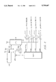
- FIG. 1 shows an abstract representation of a circuit for supplying various voltage levels to a facsimile device
- FIG. 2 shows a power saving circuit for a facsimile device constructed according to the principles of the present invention.
- FIG. 1 an abstract representation of a circuit for supplying various voltage levels to a facsimile device is shown.
- a switching mode power supply (SMPS) 2 provides voltages having various magnitudes (e.g., +5V, +12V, -12V, +24V, etc.) to respective circuits in a facsimile device. While the facsimile device performs its general functions, a switch 4 remains in an on (i.e., closed) state under the control of a central processing unit (CPU) 6.
- CPU central processing unit
- the voltage supplied through switch 4 (i.e., +24V) is used for the components and circuitry of the facsimile device that consume a lot of operating power, such as a fan driver and a heater, etc. As indicated in FIG. 1, the various voltages are used to provide the operating state system supply power.
- central processing unit (CPU) 6 switches switch 4 to an off (i.e., open) state in order to reduce unnecessary power consumption. Therefore, in these situations, the voltage supplied through switch 4 (e.g., +24V) is not provided to the fan driver and heater.
- the facsimile device has not been used for a predetermined time period, represent the stand-by state of the facsimile device.
- SMPS switching mode power supply
- the circuit of FIG. 1 interrupts the supply of power to components and circuitry that consume a large amount of power, but still provides operating power for the remaining circuits.
- optimal power savings are not achieved with the circuit shown in FIG. 1.
- the circuit of FIG. 2 includes a switching mode power supply (SMPS) 2 for supplying first, second, third and fourth voltages to first, second, third and fourth switches 10-1, 10-2, 10-3 and 10-4, respectively.
- SMPS switching mode power supply
- First, second, third and fourth switches 10-1, 10-2, 10-3 and 10-4 are switched off in response to a first state of a switching control signal (SC), and thereby interrupt the supply of first, second, third and fourth voltages to first, second, third and fourth corresponding circuits.
- SC switching control signal
- first, second, third and fourth switches 10-1, 10-2, 10-3 and 10-4 are switched on in response to a second state of switching control signal (SC), and thereby provide first, second, third and fourth voltages to first, second, third and fourth corresponding circuits.
- the first, second, third and fourth circuits each represent one or more components of the facsimile device that utilize a corresponding voltage level.
- a photo coupler 8 detects a speech forming signal applied from a central office line (COL) and outputs a driving signal (DRV) to a central processing unit (CPU) 6.
- a fifth switch 12 receives a manual power supply signal (MPS) corresponding to a user input selection, and also provides output of a power control signal (PWC) to central processing unit (CPU) 6.
- MPS manual power supply signal
- PWC power control signal
- Central processing unit (CPU) 6 generates switching control signal (SC) in a first state (i.e., the first switching control signal) to switch first, second, third and fourth switches 10-1, 10-2, 10-3 and 10-4 off when the user does not use the facsimile device for a predetermined time period, and generates switching control signal (SC) in a second state (i.e., the second switching control signal) to switch first, second, third and fourth switches 10-1, 10-2, 10-3 and 10-4 on in response to driving signal (DRV) output from photo coupler 8.
- SC switching control signal
- DUV driving signal
- switching mode power supply (SMPS) 2 provides the various voltages (i.e., +5V, +12 V, -12V, +24V) to respective circuits through first, second, third and fourth switches 10-1, 10-2, 10-3 and 10-4, respectively. During this time, the first to fourth switches 10-1 to 10-4 remain in the on state under the control of central processing unit (CPU) 6. As the respective circuits in the facsimile device receive requisite operating power, the facsimile device can perform its normal functions.
- Switching mode power supply (SMPS) 2 also provides a power supply voltage Vcc to specific circuit components, namely central processing unit (CPU) 6, a transistor of photo coupler 8 and one end of fifth switch 12.
- central processing unit (CPU) 6 applies switching control signal (SC) in a first state to first, second, third and fourth switches 10-1, 10-2, 10-3 and 10-4 to thereby switch them to the off state. Accordingly, all operating power that is provided to predetermined circuits through switches 10-1, 10-2, 10-3 and 10-4 is interrupted.
- switching mode power supply (SMPS) 2 continues to provide power supply voltage Vcc to central processing unit (CPU) 6, the transistor of photo coupler 8 and the one end of fifth switch 12 to enable their respective operations.
- the circuits in the facsimile device are provided with corresponding levels of operating power.
- a signal related to a driving operation of the facsimile device e.g., a ring signal or manual power supply signal (MPS)
- MPS manual power supply signal
- photo coupler 8 If the ring signal is applied to photo coupler 8 through the central office line (COL) while the facsimile device is in the stand-by state, photo coupler 8 outputs driving signal (DRV) to central processing unit (CPU) 6.
- central processing unit (CPU) 6 In response to receipt of driving signal (DRV), central processing unit (CPU) 6 applies switching control signal (SC) in a second state to the first to fourth switches 10-1 to 10-4, thus controlling these four switches to be in the on state.
- SC switching control signal
- the voltages +5V, +12V, -12V, +24V are provided from switching mode power supply (SMPS) 2 to respective circuits through the first to fourth switches 10-1 to 10-4, so that the facsimile device can perform its normal functions.
- SMPS switching mode power supply
- fifth switch 12 for controlling the manual power supply.
- MPS manual power supply signal
- Fifth switch 12 is preferably constructed as a switch that operates in response to depression of a given key on a keypad of the facsimile device.
- the present invention selectively provides operating voltages to circuit components of a facsimile device to thereby conserve operating power.
- an external driving signal or speech forming signal are applied, all of the circuits are provided with voltage. Accordingly, the present invention provides an advantage of reducing power consumption when a user does not use the facsimile device for a predetermined time period.
Abstract
A power saving facsimile includes a power supply circuit for supplying a plurality of voltage levels. A switch disconnects and connects the plurality of voltage levels from and to corresponding circuits in response to first and second states of a switching control signal, respectively. A driving signal output circuit outputs a driving signal in response to sensing a speech forming signal applied from a central office line. A power controller generates the switching control signal in the first state to interrupt the voltages when the facsimile device has not been used for a predetermined time period, and generates the switching control signal in the second state to provide the voltages in response to the driving signal.
Description
This application makes reference to, incorporates the same herein, and claims all benefits accruing under 35 U.S.C. §119 from an application for Power Saving Facsimile Device earlier filed in the Korean Industrial Property Office on 27 Jan. 1995 and there assigned Ser. No. 1626/1995.
The present invention relates to a facsimile device, and more particularly, to a power saving facsimile device capable of reducing power consumption by being provided with only a minimum level of power when not used for a given time period.
Recently, an energy star computer program sponsored by the U.S. Environmental Protection Agency (EPA) allows manufacturers of energy efficient office equipment complying with specified contractual terms and conditions to use a designated energy star logo indicating the energy efficiency of their product. The energy star computer program is a cooperative effort between the U.S. Environmental Protection Agency and computer device manufacturers to promote the production and sale of energy efficient office equipment. The program is particularly aimed at reducing air pollution resulting from the generation of power necessary to operate currently available office equipment. Accordingly, the program encourages the production of office equipment having power saving features. Such equipment consumes less power, and thus helps reduce the production of air pollution.
An early prior art reference directed towards the conservation of electrical energy is disclosed in U.S. Pat. No. 4,747,041 entitled Automatic Power Control System Which Automatically Activates And Deactivates Power To Selected Peripheral Devices Based Upon System Requirement issued to Engel et al. In Engel et al. '041, a controller provides selective, non-manual power control of various components of data processing equipment, and reports the power status of such components to a central location. While this early effort to conserve electrical energy is certainly useful in its own right, I note that there is a need in the realm of office equipment for a power saving facsimile device. Accordingly, the present invention recognizes and addresses this need.
It is therefore an object of the present invention to provide a power saving facsimile device capable of reducing power consumption.
It is another object to provide a power saving facsimile device capable of reducing power consumption by providing the facsimile device with only a minimum level of power when not used for a predetermined time period.
It is still another object to provide a power saving facsimile device capable of achieving a degree of power consumption while the facsimile device is in a stand-by state.
To achieve these and other objects, the present invention provides a facsimile device including a power supply circuit for supplying a plurality of voltage levels. A switch disconnects and connects the plurality of voltage levels from and to corresponding circuits in response to first and second states of a switching control signal, respectively. A driving signal output circuit outputs a driving signal in response to sensing a speech forming signal applied from a central office line. A power controller generates the switching control signal in the first state to interrupt the voltages when the facsimile device has not been used for a predetermined time period, and generates the switching control signal in the second state to provide the voltages in response to the driving signal.
A more complete appreciation of the invention, and many of the attendant advantages thereof, will be readily apparent as the same becomes better understood by reference to the following detailed description when considered in conjunction with the accompanying drawings, wherein:
FIG. 1 shows an abstract representation of a circuit for supplying various voltage levels to a facsimile device; and
FIG. 2 shows a power saving circuit for a facsimile device constructed according to the principles of the present invention.
Turn now to the drawings and referring to FIG. 1, an abstract representation of a circuit for supplying various voltage levels to a facsimile device is shown. In FIG. 1, a switching mode power supply (SMPS) 2 provides voltages having various magnitudes (e.g., +5V, +12V, -12V, +24V, etc.) to respective circuits in a facsimile device. While the facsimile device performs its general functions, a switch 4 remains in an on (i.e., closed) state under the control of a central processing unit (CPU) 6. The voltage supplied through switch 4 (i.e., +24V) is used for the components and circuitry of the facsimile device that consume a lot of operating power, such as a fan driver and a heater, etc. As indicated in FIG. 1, the various voltages are used to provide the operating state system supply power.
In FIG. 1, if the user does not use the facsimile device for a predetermined time period, central processing unit (CPU) 6 switches switch 4 to an off (i.e., open) state in order to reduce unnecessary power consumption. Therefore, in these situations, the voltage supplied through switch 4 (e.g., +24V) is not provided to the fan driver and heater. These situations, when the facsimile device has not been used for a predetermined time period, represent the stand-by state of the facsimile device. In the stand-by state, however, the voltages supplied from switching mode power supply (SMPS) 2, (i.e., +5V, +12V, -12V, +24V, which are used to provide the stand-by state system supply power, are still provided to predetermined circuits of the facsimile device.
Accordingly, in the stand-by state, the circuit of FIG. 1 interrupts the supply of power to components and circuitry that consume a large amount of power, but still provides operating power for the remaining circuits. Thus, optimal power savings are not achieved with the circuit shown in FIG. 1.
Referring now to FIG. 2, a power saving circuit for a facsimile device constructed according to the principles of the present invention is shown. The circuit of FIG. 2 includes a switching mode power supply (SMPS) 2 for supplying first, second, third and fourth voltages to first, second, third and fourth switches 10-1, 10-2, 10-3 and 10-4, respectively. First, second, third and fourth switches 10-1, 10-2, 10-3 and 10-4 are switched off in response to a first state of a switching control signal (SC), and thereby interrupt the supply of first, second, third and fourth voltages to first, second, third and fourth corresponding circuits. Similarly, first, second, third and fourth switches 10-1, 10-2, 10-3 and 10-4 are switched on in response to a second state of switching control signal (SC), and thereby provide first, second, third and fourth voltages to first, second, third and fourth corresponding circuits. The first, second, third and fourth circuits each represent one or more components of the facsimile device that utilize a corresponding voltage level. A photo coupler 8 detects a speech forming signal applied from a central office line (COL) and outputs a driving signal (DRV) to a central processing unit (CPU) 6. A fifth switch 12 receives a manual power supply signal (MPS) corresponding to a user input selection, and also provides output of a power control signal (PWC) to central processing unit (CPU) 6. Central processing unit (CPU) 6 generates switching control signal (SC) in a first state (i.e., the first switching control signal) to switch first, second, third and fourth switches 10-1, 10-2, 10-3 and 10-4 off when the user does not use the facsimile device for a predetermined time period, and generates switching control signal (SC) in a second state (i.e., the second switching control signal) to switch first, second, third and fourth switches 10-1, 10-2, 10-3 and 10-4 on in response to driving signal (DRV) output from photo coupler 8.
The operation of the present invention will now be described in detail with reference to FIG. 2.
In FIG. 2, when the facsimile device performs its normal functions, switching mode power supply (SMPS) 2 provides the various voltages (i.e., +5V, +12 V, -12V, +24V) to respective circuits through first, second, third and fourth switches 10-1, 10-2, 10-3 and 10-4, respectively. During this time, the first to fourth switches 10-1 to 10-4 remain in the on state under the control of central processing unit (CPU) 6. As the respective circuits in the facsimile device receive requisite operating power, the facsimile device can perform its normal functions. Switching mode power supply (SMPS) 2 also provides a power supply voltage Vcc to specific circuit components, namely central processing unit (CPU) 6, a transistor of photo coupler 8 and one end of fifth switch 12.
In the stand-by state that occurs when the user does not use the facsimile device for a predetermined time period, central processing unit (CPU) 6 applies switching control signal (SC) in a first state to first, second, third and fourth switches 10-1, 10-2, 10-3 and 10-4 to thereby switch them to the off state. Accordingly, all operating power that is provided to predetermined circuits through switches 10-1, 10-2, 10-3 and 10-4 is interrupted. In the stand-by state, switching mode power supply (SMPS) 2 continues to provide power supply voltage Vcc to central processing unit (CPU) 6, the transistor of photo coupler 8 and the one end of fifth switch 12 to enable their respective operations. When a signal related to a driving operation of the facsimile device (e.g., a ring signal or manual power supply signal (MPS)) is generated during the stand-by state, the circuits in the facsimile device are provided with corresponding levels of operating power.
If the ring signal is applied to photo coupler 8 through the central office line (COL) while the facsimile device is in the stand-by state, photo coupler 8 outputs driving signal (DRV) to central processing unit (CPU) 6. In response to receipt of driving signal (DRV), central processing unit (CPU) 6 applies switching control signal (SC) in a second state to the first to fourth switches 10-1 to 10-4, thus controlling these four switches to be in the on state. Accordingly, the voltages +5V, +12V, -12V, +24V are provided from switching mode power supply (SMPS) 2 to respective circuits through the first to fourth switches 10-1 to 10-4, so that the facsimile device can perform its normal functions.
If a user wants to perform an operation with the facsimile device, such as calling or printing, during the stand-by state, the user presses fifth switch 12 for controlling the manual power supply. In response to depression of fifth switch 12, manual power supply signal (MPS) is applied to fifth switch 12, and fifth switch 12 switches to the on state. Fifth switch 12 is preferably constructed as a switch that operates in response to depression of a given key on a keypad of the facsimile device.
When fifth switch 12 shifts to the on state in response to manual power supply signal (MPS), power control signal (PWC) corresponding to power supply voltage Vcc is applied to central processing unit (CPU) 6. In response to power control signal (PWC), central processing unit (CPU) 6 provides switching control signal (SC) in a second state to the first to fourth switches 10-1 to 10-4 so that these switches shift to the on state. Accordingly, respective circuits in the facsimile device are provided with corresponding voltages applied from switching mode power supply (SMPS) 2, and the facsimile device can perform its normal functions.
As described above, the present invention selectively provides operating voltages to circuit components of a facsimile device to thereby conserve operating power. When an external driving signal or speech forming signal are applied, all of the circuits are provided with voltage. Accordingly, the present invention provides an advantage of reducing power consumption when a user does not use the facsimile device for a predetermined time period.
While there have been illustrated and described what are considered to be preferred embodiments of the present invention, it will be understood by those skilled in the art that various changes and modifications may be made, and equivalents may be substituted for elements thereof without departing from the true scope of the present invention. In addition, many modifications may be made to adapt a particular situation to the teaching of the present invention without departing from the central scope thereof. Therefore, it is intended that the present invention not be limited to the particular embodiments disclosed as the best mode contemplated for carrying out the present invention, but that the present invention includes all embodiments falling within the scope of the appended claims.
Claims (16)
1. A power saving facsimile device, comprising:
power supply means for supplying a plurality of voltages having various magnitudes;
switching means for disconnecting said power supply means from corresponding circuits in response to a first switching control signal, and for connecting said power supply means to said corresponding circuits in response to a second switching control signal;
driving signal output means for outputting a driving signal in response to a ring signal provided via an office line; and
power control means for detecting when said facsimile device has not been used for a predetermined time period and for generating said first switching control signal in response thereto, and for generating said second switching control signal in response to said driving signal.
2. The power saving facsimile device as claimed in claim 1, further comprising manual power supply means for outputting a power control signal in response to a user input for enabling said power control means to generate said second switching control signal.
3. The power saving facsimile device as claimed in claim 2, wherein said manual power supply means comprises a switching device that is switched on in response to said user input.
4. The power saving facsimile device as claimed in claim 1, wherein said driving signal output means comprises a photo coupler for outputting said driving signal in response to said ring signal provided via said office line.
5. The power saving facsimile device as claimed in claim 3, wherein said driving signal output means comprises a photo coupler for outputting said driving signal in response to said ring signal provided via said office line.
6. A power saving facsimile device, comprising:
power supply means for supplying first, second, third and fourth voltages;
first, second, third and fourth switching means for disconnecting said power supply means from first, second, third and fourth circuits in response to a first switching control signal, and for respectively connecting said power supply means to said first, second, third and fourth circuits in response to a second switching control signal;
driving signal output means for outputting a driving signal in response to a ring signal provided via an office line;
manual power supply means for outputting a power control signal in response to a user input; and
power control means for detecting when said facsimile device has not been used for a predetermined time period and for generating said first switching control signal in response thereto, and for generating said second switching control signal in response to one of said driving signal and said power control signal.
7. The power saving facsimile device as claimed in claim 6, wherein said manual power supply means comprises a switching device that is switched on in response to said user input.
8. The power saving facsimile device as claimed in claim 6, wherein said driving signal output means comprises a photo coupler for outputting said driving signal in response to said ring signal provided via said office line.
9. The power saving facsimile device as claimed in claim 7, wherein said driving signal output means comprises a photo coupler for outputting said driving signal in response to said ring signal provided via said office line.
10. The power saving facsimile device as claimed in claim 6, further comprised of said power supply means for supplying a predetermined voltage to said driving signal output means, said manual power supply means and said power control means.
11. A facsimile device, comprising:
power supply means for supplying first, second, third and fourth voltages;
switching means for disconnecting said power supply means from corresponding circuits in response to a first switching control signal, and for connecting said power supply means to said corresponding circuits in response to a second switching control signal;
driving signal output means for outputting a driving signal in response to a ring signal provided via an office line; and
power control means for detecting a stand-by state when said facsimile device has not been used for a predetermined time period and for generating said first switching control signal in response thereto, and for generating said second switching control signal in response to said driving signal.
12. The facsimile device as claimed in claim 11, further comprising manual power supply means for outputting a power control signal in response to a user input for enabling said power control means to generate said second switching control signal.
13. The power saving facsimile device as claimed in claim 12, wherein said manual power supply means comprises a switching device that is switched on in response to said user input.
14. The power saving facsimile device as claimed in claim 11, wherein said driving signal output means comprises a photo coupler for outputting said driving signal in response to said ring signal provided via said office line.
15. The power saving facsimile device as claimed in claim 12, further comprised of said power supply means for supplying a predetermined voltage to said driving signal output means, said manual power supply means and said power control means.
16. A method for saving power in a facsimile device, comprising the steps of:
disconnecting a power supply means which supplies a plurality of voltages from corresponding circuits within said facsimile device in response to detection of activation of a stand-by state wherein said facsimile device has not been used for a predetermined time period; and
connecting said power supply means which supplies said plurality of voltages to said corresponding circuits in response to said facsimile device receiving one of a ring signal via a communication line and a manual key input from a user.
Applications Claiming Priority (2)
| Application Number | Priority Date | Filing Date | Title |
|---|---|---|---|
| KR1019950001626A KR960030631A (en) | 1995-01-27 | 1995-01-27 | Energy-saving fax |
| KR1626/1995 | 1995-01-27 |
Publications (1)
| Publication Number | Publication Date |
|---|---|
| US5729667A true US5729667A (en) | 1998-03-17 |
Family
ID=19407446
Family Applications (1)
| Application Number | Title | Priority Date | Filing Date |
|---|---|---|---|
| US08/593,403 Expired - Lifetime US5729667A (en) | 1995-01-27 | 1996-01-29 | Power saving facsimile device |
Country Status (4)
| Country | Link |
|---|---|
| US (1) | US5729667A (en) |
| KR (1) | KR960030631A (en) |
| DE (1) | DE19545918A1 (en) |
| GB (1) | GB2297452B (en) |
Cited By (11)
| Publication number | Priority date | Publication date | Assignee | Title |
|---|---|---|---|---|
| US5894543A (en) * | 1994-10-20 | 1999-04-13 | Canon Kabushiki Kaisha | Facsimile apparatus having two states of operation which are controlled in response to discriminating an operational condition |
| US6035205A (en) * | 1997-03-07 | 2000-03-07 | Samsung Electronics Co., Ltd. | Apparatus and method for enhancing telephone call quality of facsimile system with wireless telephone function |
| EP0996233A2 (en) * | 1998-10-22 | 2000-04-26 | Lg Electronics Inc. | Apparatus and method for controlling power saving mode in a power supply |
| EP1067753A2 (en) * | 1999-07-08 | 2001-01-10 | Ricoh Company, Ltd. | Electronic mail terminal device and method of controlling the same |
| US6330175B2 (en) * | 2000-02-02 | 2001-12-11 | Sony Corporation | Power supply apparatus for electronic unit |
| US20040233475A1 (en) * | 2000-07-18 | 2004-11-25 | Canon Kabushiki Kaisha | Image capture apparatus capable of being wirelessly connected to other apparatuses; and method for controlling the same |
| US20050278554A1 (en) * | 2004-06-10 | 2005-12-15 | Digi International Inc. | System and method for routing data and power to external devices |
| EP1736834A1 (en) * | 2005-06-25 | 2006-12-27 | Samsung Electronics Co, Ltd | High Voltage Power Supply and Digital Control Method Thereof |
| US20070070384A1 (en) * | 2005-09-27 | 2007-03-29 | Samsung Electronics Co., Ltd. | Ultra-power saving facsimile apparatus and method thereof |
| US20070236734A1 (en) * | 2006-04-05 | 2007-10-11 | Sharp Kabushiki Kaisha | Image processing apparatus |
| CN100454189C (en) * | 2006-01-05 | 2009-01-21 | 三星电子株式会社 | Power saving apparatus |
Families Citing this family (1)
| Publication number | Priority date | Publication date | Assignee | Title |
|---|---|---|---|---|
| US5758040A (en) * | 1995-01-26 | 1998-05-26 | Ricoh Company, Ltd. | Energy-saving facsimile apparatus and energy-saving method for facsimile apparatus |
Citations (12)
| Publication number | Priority date | Publication date | Assignee | Title |
|---|---|---|---|---|
| US4747041A (en) * | 1983-06-27 | 1988-05-24 | Unisys Corporation | Automatic power control system which automatically activates and deactivates power to selected peripheral devices based upon system requirement |
| US5003578A (en) * | 1989-08-11 | 1991-03-26 | Lin Den K | Power-saving device for a cable-information receiving/transmitting apparatus |
| JPH03108941A (en) * | 1989-09-22 | 1991-05-09 | Ricoh Co Ltd | Facsimile equipment |
| US5163124A (en) * | 1987-10-14 | 1992-11-10 | Sharp Kabushiki Kaisha | Method and apparatus for controlling power to device in a computer system |
| US5282054A (en) * | 1991-05-16 | 1994-01-25 | Tokyo Electric Co., Ltd. | Facsimile equipment having different operations with different power sources |
| US5325209A (en) * | 1991-04-18 | 1994-06-28 | Ricoh Company, Ltd. | Multiplex image forming apparatus |
| US5347167A (en) * | 1990-08-09 | 1994-09-13 | Sophisticated Circuits, Inc. | Power controller using keyboard and computer interface |
| US5392023A (en) * | 1991-09-06 | 1995-02-21 | Motorola, Inc. | Data communication system with automatic power control |
| US5475500A (en) * | 1993-02-22 | 1995-12-12 | Canon Kabushiki Kaisha | Image processing apparatus having a remote mode for printing data from an external apparatus and a local mode for recording an image read by a copier |
| US5483464A (en) * | 1993-03-31 | 1996-01-09 | Samsung Electronics Co., Ltd. | Power saving apparatus for use in peripheral equipment of a computer |
| EP0701361A2 (en) * | 1994-09-07 | 1996-03-13 | Canon Kabushiki Kaisha | A facsimile machine |
| US5528385A (en) * | 1993-10-08 | 1996-06-18 | Zoom Telephonics, Inc. | Faxmodem with scanning capability |
Family Cites Families (3)
| Publication number | Priority date | Publication date | Assignee | Title |
|---|---|---|---|---|
| GB2231213A (en) * | 1989-02-24 | 1990-11-07 | Pyramid Power Systems Limited | An uninterruptible power supply for a facsimile machine |
| KR960010183B1 (en) * | 1993-10-23 | 1996-07-26 | 김광호 | Image recording apparatus and control method thereof for energy economization |
| KR0141675B1 (en) * | 1993-12-30 | 1998-07-15 | 김광호 | Method to print with saving power in electronic image forming device |
-
1995
- 1995-01-27 KR KR1019950001626A patent/KR960030631A/en not_active IP Right Cessation
- 1995-12-08 DE DE19545918A patent/DE19545918A1/en not_active Ceased
-
1996
- 1996-01-18 GB GB9600988A patent/GB2297452B/en not_active Expired - Fee Related
- 1996-01-29 US US08/593,403 patent/US5729667A/en not_active Expired - Lifetime
Patent Citations (12)
| Publication number | Priority date | Publication date | Assignee | Title |
|---|---|---|---|---|
| US4747041A (en) * | 1983-06-27 | 1988-05-24 | Unisys Corporation | Automatic power control system which automatically activates and deactivates power to selected peripheral devices based upon system requirement |
| US5163124A (en) * | 1987-10-14 | 1992-11-10 | Sharp Kabushiki Kaisha | Method and apparatus for controlling power to device in a computer system |
| US5003578A (en) * | 1989-08-11 | 1991-03-26 | Lin Den K | Power-saving device for a cable-information receiving/transmitting apparatus |
| JPH03108941A (en) * | 1989-09-22 | 1991-05-09 | Ricoh Co Ltd | Facsimile equipment |
| US5347167A (en) * | 1990-08-09 | 1994-09-13 | Sophisticated Circuits, Inc. | Power controller using keyboard and computer interface |
| US5325209A (en) * | 1991-04-18 | 1994-06-28 | Ricoh Company, Ltd. | Multiplex image forming apparatus |
| US5282054A (en) * | 1991-05-16 | 1994-01-25 | Tokyo Electric Co., Ltd. | Facsimile equipment having different operations with different power sources |
| US5392023A (en) * | 1991-09-06 | 1995-02-21 | Motorola, Inc. | Data communication system with automatic power control |
| US5475500A (en) * | 1993-02-22 | 1995-12-12 | Canon Kabushiki Kaisha | Image processing apparatus having a remote mode for printing data from an external apparatus and a local mode for recording an image read by a copier |
| US5483464A (en) * | 1993-03-31 | 1996-01-09 | Samsung Electronics Co., Ltd. | Power saving apparatus for use in peripheral equipment of a computer |
| US5528385A (en) * | 1993-10-08 | 1996-06-18 | Zoom Telephonics, Inc. | Faxmodem with scanning capability |
| EP0701361A2 (en) * | 1994-09-07 | 1996-03-13 | Canon Kabushiki Kaisha | A facsimile machine |
Cited By (18)
| Publication number | Priority date | Publication date | Assignee | Title |
|---|---|---|---|---|
| US5894543A (en) * | 1994-10-20 | 1999-04-13 | Canon Kabushiki Kaisha | Facsimile apparatus having two states of operation which are controlled in response to discriminating an operational condition |
| US6035205A (en) * | 1997-03-07 | 2000-03-07 | Samsung Electronics Co., Ltd. | Apparatus and method for enhancing telephone call quality of facsimile system with wireless telephone function |
| EP0996233A2 (en) * | 1998-10-22 | 2000-04-26 | Lg Electronics Inc. | Apparatus and method for controlling power saving mode in a power supply |
| EP0996233A3 (en) * | 1998-10-22 | 2003-11-12 | Lg Electronics Inc. | Apparatus and method for controlling power saving mode in a power supply |
| US6883016B1 (en) | 1999-07-08 | 2005-04-19 | Ricoh Company, Ltd. | Electronic mail terminal device and method of controlling the same |
| EP1067753A2 (en) * | 1999-07-08 | 2001-01-10 | Ricoh Company, Ltd. | Electronic mail terminal device and method of controlling the same |
| EP1067753A3 (en) * | 1999-07-08 | 2002-09-04 | Ricoh Company, Ltd. | Electronic mail terminal device and method of controlling the same |
| US6330175B2 (en) * | 2000-02-02 | 2001-12-11 | Sony Corporation | Power supply apparatus for electronic unit |
| US20040233475A1 (en) * | 2000-07-18 | 2004-11-25 | Canon Kabushiki Kaisha | Image capture apparatus capable of being wirelessly connected to other apparatuses; and method for controlling the same |
| US7907297B2 (en) * | 2000-07-18 | 2011-03-15 | Canon Kabushiki Kaisha | Image capture apparatus capable of communicating wirelessly and reducing power consumption, and method for controlling the same |
| US9049319B2 (en) | 2000-07-18 | 2015-06-02 | Canon Kabushiki Kaisha | Image communication apparatus wirelessly connectable to other apparatuses, system having the image communication apparatus, and method for controlling the same |
| US20050278554A1 (en) * | 2004-06-10 | 2005-12-15 | Digi International Inc. | System and method for routing data and power to external devices |
| US7240229B2 (en) * | 2004-06-10 | 2007-07-03 | Digi International Inc. | System and method for routing data and power to external devices |
| EP1736834A1 (en) * | 2005-06-25 | 2006-12-27 | Samsung Electronics Co, Ltd | High Voltage Power Supply and Digital Control Method Thereof |
| US20070070384A1 (en) * | 2005-09-27 | 2007-03-29 | Samsung Electronics Co., Ltd. | Ultra-power saving facsimile apparatus and method thereof |
| CN100454189C (en) * | 2006-01-05 | 2009-01-21 | 三星电子株式会社 | Power saving apparatus |
| US20070236734A1 (en) * | 2006-04-05 | 2007-10-11 | Sharp Kabushiki Kaisha | Image processing apparatus |
| US7872774B2 (en) * | 2006-04-05 | 2011-01-18 | Sharp Kabushiki Kaisha | Image processing apparatus having an energization switching unit and control information updating unit |
Also Published As
| Publication number | Publication date |
|---|---|
| GB2297452B (en) | 1997-03-26 |
| GB9600988D0 (en) | 1996-03-20 |
| GB2297452A (en) | 1996-07-31 |
| KR960030631A (en) | 1996-08-17 |
| DE19545918A1 (en) | 1996-08-08 |
Similar Documents
| Publication | Publication Date | Title |
|---|---|---|
| KR100393062B1 (en) | Double control unit capable of saving power and power control method thereof | |
| US5729667A (en) | Power saving facsimile device | |
| US6665806B1 (en) | Power saving for a portable information processing apparatus using switch that shuts off power to sub memory block when in battery mode and supplies power when in AC mode | |
| US6006335A (en) | Power management system and method of displaying power management information in a computer | |
| US5546591A (en) | Distributed power management system for battery operated personal computers | |
| JP2000324713A (en) | Controller for charging current | |
| US5758103A (en) | Circuit for replacing a peripheral device of a computer system and method therefor | |
| JP2004202692A (en) | Image formation device | |
| US5692203A (en) | Power up/power down for electronic hardware which conserves electric power | |
| KR20070075106A (en) | Power supply apparatus and display apparatus having the same | |
| EP0172344A2 (en) | Power saving system | |
| US5555167A (en) | Power supply apparatus with a power-saving function | |
| US20090157231A1 (en) | Washing machine and controlling method for the same | |
| KR20100045377A (en) | Image forming apparatus and control method thereof | |
| JP2003319572A (en) | Power control system for indoor equipment | |
| JPH11167439A (en) | Information processor having power selection state of multiple stages | |
| KR100480017B1 (en) | Apparatus and method for controlling power saving in display | |
| JPH10173840A (en) | Facsimile equipment | |
| JP2004127188A (en) | Information processing system | |
| US7308585B2 (en) | Low power residual remaining power indicator | |
| KR0135742Y1 (en) | Power saving device for image display apparatus | |
| JP3575355B2 (en) | RGB signal input switching device and power consumption reduction method | |
| KR970008816A (en) | Power saving device of printer by power off mode | |
| JP2006211499A (en) | Image forming system | |
| KR960043449A (en) | Power saving device for office equipment |
Legal Events
| Date | Code | Title | Description |
|---|---|---|---|
| AS | Assignment |
Owner name: SAMSUNG ELECTRONICS CO., LTD., A CORP. OF KOREA, K Free format text: ASSIGNMENT OF ASSIGNORS INTEREST;ASSIGNOR:LEE, GANG-BOCK;REEL/FRAME:007864/0122 Effective date: 19960311 |
|
| STCF | Information on status: patent grant |
Free format text: PATENTED CASE |
|
| FEPP | Fee payment procedure |
Free format text: PAYOR NUMBER ASSIGNED (ORIGINAL EVENT CODE: ASPN); ENTITY STATUS OF PATENT OWNER: LARGE ENTITY |
|
| FPAY | Fee payment |
Year of fee payment: 4 |
|
| FPAY | Fee payment |
Year of fee payment: 8 |
|
| FPAY | Fee payment |
Year of fee payment: 12 |