US5690781A - Plasma processing apparatus for manufacture of semiconductor devices - Google Patents
Plasma processing apparatus for manufacture of semiconductor devices Download PDFInfo
- Publication number
- US5690781A US5690781A US08/527,847 US52784795A US5690781A US 5690781 A US5690781 A US 5690781A US 52784795 A US52784795 A US 52784795A US 5690781 A US5690781 A US 5690781A
- Authority
- US
- United States
- Prior art keywords
- coil
- dielectric plate
- reaction chamber
- chamber
- main surface
- Prior art date
- Legal status (The legal status is an assumption and is not a legal conclusion. Google has not performed a legal analysis and makes no representation as to the accuracy of the status listed.)
- Expired - Fee Related
Links
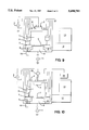
Images


Classifications
-
- H—ELECTRICITY
- H01—ELECTRIC ELEMENTS
- H01J—ELECTRIC DISCHARGE TUBES OR DISCHARGE LAMPS
- H01J37/00—Discharge tubes with provision for introducing objects or material to be exposed to the discharge, e.g. for the purpose of examination or processing thereof
- H01J37/32—Gas-filled discharge tubes
- H01J37/32009—Arrangements for generation of plasma specially adapted for examination or treatment of objects, e.g. plasma sources
- H01J37/32082—Radio frequency generated discharge
- H01J37/321—Radio frequency generated discharge the radio frequency energy being inductively coupled to the plasma
-
- H—ELECTRICITY
- H01—ELECTRIC ELEMENTS
- H01J—ELECTRIC DISCHARGE TUBES OR DISCHARGE LAMPS
- H01J37/00—Discharge tubes with provision for introducing objects or material to be exposed to the discharge, e.g. for the purpose of examination or processing thereof
- H01J37/32—Gas-filled discharge tubes
- H01J37/32431—Constructional details of the reactor
- H01J37/32458—Vessel
Definitions
- the present invention relates to an apparatus for plasma processing used for the manufacture of semiconductor devices.
- etching is performed by the combined action of neutral radicals and ions formed in a plasma generated within a reaction chamber. Ions in the plasma are accelerated through the action of electric fields created in the reaction chamber to hit the wafer. However, these ions are scattered due to collision with neutral gas molecules, resulting in a change in the direction of movement. Therefore, these ions cannot strike the wafer surface perpendicularly, thus causing lateral etching (frequently called "side etching"), resulting in formation of etched structures different in geometric size from the mask.
- side etching lateral etching
- the number of neutral-gas molecules may be decreased to reduce the collision of ions with the neutral-gas molecules by lowering gas pressure in the reaction chamber.
- the density of the plasma itself also decreases, insufficient etching selectivity, i.e., insufficient etching rate difference for different materials becomes a problem, pertaining to the different material underlying the material to be etched. Therefore, apparatuses using high density plasma sources for producing plasma with sufficient density in a low pressure region have been proposed.
- FIG. 13 shows the structure of this apparatus.
- a magnetic field penetrating through a dielectric plate 55 and parallel to the dielectric plate 55 is generated in a reaction chamber 52 by flowing an RF current through a coil 45 having a planar side.
- the fluctuation in the thus generated magnetic field over time further produces an inductive electric field by electromagnetic induction, which in turn generates a low-pressure, high-concentration plasma.
- ion energy incident to a to be ached wafer 59 is controlled by placing the wafer 59 on an electrode 56 installed in the reaction chamber 52 to face the dielectric plate 55, and simultaneously biasing this electrode to a certain voltage.
- the diameter of the coil 45 is smaller at the end than at the center in order to make the intensity of the generated magnetic field uniform.
- the coil used for producing plasma is not symmetrical about the center of the reaction chamber where the to be processed wafer is placed. Therefore, the density of the plasma produced is also not axially symmetrical, and achieving a uniform plasma cannot be expected. Since the uniformity of the plasma affects the uniformity of the etching rate directly, acceptable uniformity of the etching rate, which is one of important parameters of etching, cannot be expected.
- etching conditions were required to be changed in order to control the etching selectivity and etching profiles.
- a uniform plasma and a uniform etching rate is achieved by making the dielectric plate thick at the center of the reaction chamber and thin at the peripheral portion of the chamber. Uniformity of the plasma and the etching rate is further achieved by forming the electric field induced by supplying an RF current to the coil to be axially symmetrical about the center of the reaction chamber.
- the etching profile and the selectivity are controlled by varying the distance between the dielectric plate and the spiral coil.
- FIG. 1(a) is a schematic drawing illustrating a first embodiment of the present invention having a dielectric plate window which is thicker at the center of the reaction chamber, thinner at the periphery, and convex downward;
- FIG. 1(b) is a schematic drawing illustrating the spiral coil of the first embodiment of the present invention
- FIG. 2(a) shows schematically by arrows, the direction of the magnetic field produced by application of an RF voltage to the spiral coil
- FIG. 2(b) shows schematically by arrows, the direction of the electric field produced by application of an RF voltage to the spiral coil
- FIG. 3 shows 3 different plots of ion current density distribution for 3 types of dielectric plate window shapes
- FIG. 4(a) shows, for n + -type polysilicon etching, the dependency of the etching rate and uniformity on the shape of the dielectric plate window;
- FIG. 4(b) shows, for WSi 2 etching, the dependency of the etching rate and uniformity on the shape of the dielectric plate window
- FIG. 5(a) schematically illustrates a second embodiment of the present invention, wherein a plano-convex dielectric plate window positioned to have the convex portion pointing away from the reaction chamber and a flat coil is combined;
- FIG. 5(b) schematically illustrates the second embodiment of the present invention, wherein a plano-convex dielectric plate window positioned to have the convex portion pointing away from the reaction chamber and a non-flat coil conforming to the convex shape of the plate is combined;
- FIG. 5(c) schematically illustrates the second embodiment of the present invention, wherein a dome-shaped dielectric plate window positioned to have the convex side pointing away from the reaction chamber and a curved coil conforming to the convex shape of the dome is combined;
- FIG. 6(a) is a schematic cross sectional drawing illustrating a third embodiment of the present invention, wherein a spiral coil is movable in a direction parallel to the main planar side of the dielectric plate window;
- FIG. 6(b) is a schematic drawing illustrating a top view of the third embodiment of the present invention.
- FIG. 7 shows the dependency of etching uniformity on locations in the radial direction of the coil
- FIG. 8(a) illustrates a fourth embodiment of the present invention, wherein the coil consists of a combination of two spiral coils electrically connected and the shape of the combined coil is axially symmetrical;
- FIG. 8(b) illustrates another example of the fourth embodiment of the present invention, wherein the coil consists of a combination of four spiral coils electrically connected and the shape of the combined coil is axially symmetrical;
- FIG. 9 illustrates a fifth embodiment of the present invention, wherein the shape of the coil is axially symmetrical and a plano-convex dielectric plate window positioned to have the convex portion pointing away from the reaction chamber is combined;
- FIG. 10 illustrates a sixth embodiment of the present invention, wherein the coil is movable in its axial direction
- FIG. 11(a) shows the dependency of the etching rate and etching uniformity of polysilicon on locations in the axial direction of the coil
- FIG. 11(b) shows the dependency of the etching rate and etching uniformity of SiO 2 on locations in the axial direction of the coil
- FIG. 12 shows, for two different taper angles, the etched profiles of poly-silicon when the distance between the coil and the dielectric window was varied.
- FIG. 13 illustrates an example of the related art.
- FIG. 1 illustrates a first embodiment of the plasma processing apparatus of the present invention. The method for producing a plasma and the method for using the plasma for etching will be described in detail below.
- a semiconductor wafer 7 to be processed having a diameter of, for example, 6 inches is placed in a reaction chamber 1.
- the distance between the wafer 7 and the dielectric plate window 4 is adjusted, a process gas is introduced from the gas ring 9 into the reaction chamber 1, and the pressure in the reaction chamber 1 is adjusted to, for example, several millitorr.
- a radio frequency (RF) current is supplied to a spiral coil 2 placed on the dielectric window 4 from an RF power source 3 of, for example, 13.56 MHz through a matching circuit not shown in FIG. 1.
- RF radio frequency
- This induction field 15 causes the electrons in the reaction chamber 1 to move and repeatedly collide with the gas molecules to generate plasma.
- the generated plasma contains not only the above fully inductively coupled component but also a capacitively coupled component, wherein the coil and the plasma are directly coupled.
- the wafer 7 to be processed is etched by a plasma thus generated.
- the lower electrode 8 on which the wafer 7 is placed is biased by the RF power source 11 to control the ion energy, i.e., the kinetic energy of the ions impinging on the surface of the wafer 7.
- the distribution of ion current densities in the radial direction of the reaction chamber 1 was measured by changing the shape of the dielectric window.
- Dielectric plate windows having a uniform thickness 16, and that having a thick part at the center 17, and that having of a wider thick part 18 were compared. The result of the measurement is shown in FIG. 3.
- the ion current density is high at the center, and the uniformity within a diameter of 6 inches was as low as ⁇ 15%.
- the wound conductive material of the spiral coil 2 is equally spaced and wound to end at the center of the reaction chamber, so that the intensity of the induction field produced by the coil 2 is high at the center.
- the uniformity increased to ⁇ 5%
- the dielectric window 18 having a widened thick part the uniformity was further improved to ⁇ 3%.
- the uniformity of the etching rate 19 and 21 for polysilicon and WSi 2 corresponds to the uniformity of the plasma density, and improved from ⁇ 10% to ⁇ 4% for poly-silicon and ⁇ 7% to ⁇ 2.5% for WSi 2 .
- FIG. 5(a), (b) and (c) shows a second embodiment of the present invention, wherein the dielectric plate has a plano-convex shape or a dome-like shape with the convex side pointing upward, away from the reaction chamber.
- FIG. 5(a) shows the case where a flat coil is used with the upwardly convex dielectric plate.
- FIG. 5(b) shows the case where a coil is provided to conform along the upper surface of the upwardly convex dielectric plate; and
- FIG. 5(c) shows the case where a coil is provided to conform along the upper surface of the upwardly domed dielectric plate.
- FIG. 6(a) and FIG. 6(b) show a third embodiment of the present invention for making the etching rate distribution further uniform.
- the spiral coil 2 is made movable in the direction parallel to the main planar surface of the dielectric plate, or in effect the radial direction of the reaction chamber 1 by a motor 23 and a control mechanism thereof. Since the spiral coil 2 is not axially symmetrical, the distribution of the etching rate is not symmetrical about the center of the wafer which is located on axis of the chamber. Therefore, the coil was moved ⁇ 1 cm in the radial direction 25, which creates the most change in the system, and the uniformity of etching rate of poly-silicon and WSi 2 was measured. The result is shown in FIG. 7.
- FIG. 8(a) and FIG. 8(b) show an embodiment wherein a plurality of coils are combined in order to make the coils axially symmetrical about the center.
- two and four coils, respectively are electrically connected together at the axis of the reaction chamber to form axially symmetrical shapes.
- the same plasma density is obtained by a shorter coil length.
- Decrease in the length of a coil reduces the electric resistance of the coils, and voltage applied to the coils may be lowered from several kilovolts to several hundred volts.
- the capacitively coupled component of the plasma is decreased so that sputtering of the dielectric plate is reduced, thus minimizing contamination due to the sputtered dielectric material (Si, SiO 2 or O 2 in the case of quartz, and Al or Al 2 O 3 in the case of alumina ceramics).
- FIG. 9 A fifth embodiment of the present invention is shown in FIG. 9.
- the dielectric plate window is provided outside the reaction chamber 1 and is placed to have the convex side pointing upward, away from the reaction chamber.
- An axially symmetrical coil is provided to conform along the upper surface of this dielectric plate.
- the flat side of the dielectric plate constitutes part of the inside wall of the chamber so that the maintenance of the chamber is made feasible. Also, since the center portion is thicker than the circumference, and since the coil is axially symmetrical about the center of the reaction chamber, the uniformity of the plasma and the etching rate is achieved.
- FIG. 10 shows a sixth embodiment of the present invention, wherein the coil is movable in the axial direction by use of a motor 23 and a control mechanism 24.
- the distance between the coil and the dielectric plate window can be varied for each etching step much as like varying the etching condition.
- the ratio of the inductively coupled component and the capacitively coupled component in the plasma can be changed.
- FIG. 10(a) shows the etching rate and etching uniformity for polysilicon etching observed when the distance between the coil and the dielectric window was changed.
- FIG. 11(b) shows the etching rate of SiO 2 , and the etching selectivity of poly-silicon to SiO 2 observed when the distance between the coil and the dielectric window was changed. The selectivity can be varied from 60 and 140 without changing the poly-silicon etching rate using the otherwise same etching conditions, and the process margin can be expanded.
- FIG. 12 shows two cross sectional secondary electron microscope (SEM) photographs depicting the etched profile of a poly-silicon structure observed when the distance between the coil and the dielectric window was changed. The bottom figure is a schematic drawing showing the layer structure of the observed sample.
- SEM secondary electron microscope
- the taper angle (the angle made by the side wall and the bottom surface) can be varied from 80 to 90 degrees. Therefore, the etching profile can be controlled by changing the distance between the coil and the dielectric window during a main etching step and an over-etching step.
- the uniformity of the plasma ion current density is improved from ⁇ 15% to ⁇ 3%, and the uniformity of the etching rate is improved from ⁇ 10% to ⁇ 4% for polysilicon and from ⁇ 5% to ⁇ 1% for WSi 2 .
- the etching selectivity of polysilicon to SiO 2 can be varied from 60 to 140, and the taper angle can be varied from 80 to 90 degrees, without changing etching conditions other than the axial position of the coil.
- reaction chamber was assumed to have a cylindrical shape, but it may have a non-cylindrical geometry.
- dielectric plate window may be of material other than quartz or alumina ceramics. It is intended for the subject matter of the invention to include all alternatives, modifications and equivalents as can be included within the spirit and scope of the following claims.
Abstract
A plasma processing apparatus comprises a reaction chamber to hold a high-density plasma and having a dielectric plate window, a spiral coil placed outside the reaction chamber and close to the dielectric window, and a lower electrode which holds a wafer to be processed in place and installed in the reaction chamber facing the dielectric plate. A first radio frequency current supply to the coil, a mechanism for varying the distance between the coil and the dielectric plate window, and a second radio frequency voltage supply to the lower electrode is provided. Excellent uniformity of the ion current density of the plasma and hence etching rate is achieved by making the thickness of a central part of the dielectric plate window thicker than its peripheral parts. Also, the uniformity of the plasma and the etching rate is achieved by making the induction field produced by the coil axially symmetrical about the axial center of the reaction chamber. The etching profile and the material etching selectivity are controlled by moving the coil in the axial direction of the coil.
Description
1. Field of the Invention
The present invention relates to an apparatus for plasma processing used for the manufacture of semiconductor devices.
2. Description of the Related Art
With the increase in the degree of integration, and hence the increase in the density of semiconductor devices, dry etching systems which can perform anisotropic etching on wafers are being widely used. For example, in dry etching systems using plasmas, etching is performed by the combined action of neutral radicals and ions formed in a plasma generated within a reaction chamber. Ions in the plasma are accelerated through the action of electric fields created in the reaction chamber to hit the wafer. However, these ions are scattered due to collision with neutral gas molecules, resulting in a change in the direction of movement. Therefore, these ions cannot strike the wafer surface perpendicularly, thus causing lateral etching (frequently called "side etching"), resulting in formation of etched structures different in geometric size from the mask. The number of neutral-gas molecules may be decreased to reduce the collision of ions with the neutral-gas molecules by lowering gas pressure in the reaction chamber. However, since the density of the plasma itself also decreases, insufficient etching selectivity, i.e., insufficient etching rate difference for different materials becomes a problem, pertaining to the different material underlying the material to be etched. Therefore, apparatuses using high density plasma sources for producing plasma with sufficient density in a low pressure region have been proposed.
An example of such a plasma generating apparatus is disclosed in a Japanese Laid-Open Patent Publication (Kokai), JPUPA 6-84811. FIG. 13 shows the structure of this apparatus. In this apparatus a magnetic field penetrating through a dielectric plate 55 and parallel to the dielectric plate 55 is generated in a reaction chamber 52 by flowing an RF current through a coil 45 having a planar side. The fluctuation in the thus generated magnetic field over time further produces an inductive electric field by electromagnetic induction, which in turn generates a low-pressure, high-concentration plasma. Also in this apparatus, ion energy incident to a to be ached wafer 59 is controlled by placing the wafer 59 on an electrode 56 installed in the reaction chamber 52 to face the dielectric plate 55, and simultaneously biasing this electrode to a certain voltage. The diameter of the coil 45 is smaller at the end than at the center in order to make the intensity of the generated magnetic field uniform.
In the plasma generating apparatus described above, the coil used for producing plasma is not symmetrical about the center of the reaction chamber where the to be processed wafer is placed. Therefore, the density of the plasma produced is also not axially symmetrical, and achieving a uniform plasma cannot be expected. Since the uniformity of the plasma affects the uniformity of the etching rate directly, acceptable uniformity of the etching rate, which is one of important parameters of etching, cannot be expected.
It is important that the method for making a plasma density uniform is a simple one so as to cope with the recent trend of increase in the diameter of wafers.
Also in conventional plasma generating apparatuses, etching conditions were required to be changed in order to control the etching selectivity and etching profiles.
It is therefore an object of the present invention to provide a simple plasma generating apparatus which can meet requirements of increased wafers diameters, has a low-pressure/high-concentration plasma source with a capability of producing a uniform plasma and hence a uniform etching rate.
It is another object of the present invention to provide a method for producing plasma using the apparatus for producing plasma of the present invention, and controlling the selection ratio and the shape without changing the etching conditions.
An apparatus according to the present invention for producing low pressure/high concentration plasma comprises: a reaction chamber having a plate consisting of a dielectric material at an upper part of the chamber and being electrically grounded at other parts, a spiral coil placed outside the reaction chamber in the vicinity of the upper surface of the dielectric plate, an RF power source for supplying a high frequency current to the spiral coil, a tuning means for this RF power source and the coil, a means for introducing a plurality of gases into the reaction chamber, a means for controlling the pressure of the process gases, a lower electrode provided at the lower portion of the reaction chamber and on which the processed wafers are placed, a mechanical means to vary the distance between the dielectric plate and the spiral coil, and a means for supplying the lower electrode with a high frequency voltage. A uniform plasma and a uniform etching rate is achieved by making the dielectric plate thick at the center of the reaction chamber and thin at the peripheral portion of the chamber. Uniformity of the plasma and the etching rate is further achieved by forming the electric field induced by supplying an RF current to the coil to be axially symmetrical about the center of the reaction chamber.
In the above plasma generating apparatus, the etching profile and the selectivity are controlled by varying the distance between the dielectric plate and the spiral coil.
The above-mentioned and other objects, features and advantages of this invention will become more apparent by reference to the following detailed description of the invention taken in conjunction with the accompanying drawings, wherein:
FIG. 1(a) is a schematic drawing illustrating a first embodiment of the present invention having a dielectric plate window which is thicker at the center of the reaction chamber, thinner at the periphery, and convex downward;
FIG. 1(b) is a schematic drawing illustrating the spiral coil of the first embodiment of the present invention;
FIG. 2(a) shows schematically by arrows, the direction of the magnetic field produced by application of an RF voltage to the spiral coil; and
FIG. 2(b) shows schematically by arrows, the direction of the electric field produced by application of an RF voltage to the spiral coil;
FIG. 3 shows 3 different plots of ion current density distribution for 3 types of dielectric plate window shapes;
FIG. 4(a) shows, for n+ -type polysilicon etching, the dependency of the etching rate and uniformity on the shape of the dielectric plate window; and
FIG. 4(b) shows, for WSi2 etching, the dependency of the etching rate and uniformity on the shape of the dielectric plate window;
FIG. 5(a) schematically illustrates a second embodiment of the present invention, wherein a plano-convex dielectric plate window positioned to have the convex portion pointing away from the reaction chamber and a flat coil is combined;
FIG. 5(b) schematically illustrates the second embodiment of the present invention, wherein a plano-convex dielectric plate window positioned to have the convex portion pointing away from the reaction chamber and a non-flat coil conforming to the convex shape of the plate is combined;
FIG. 5(c) schematically illustrates the second embodiment of the present invention, wherein a dome-shaped dielectric plate window positioned to have the convex side pointing away from the reaction chamber and a curved coil conforming to the convex shape of the dome is combined;
FIG. 6(a) is a schematic cross sectional drawing illustrating a third embodiment of the present invention, wherein a spiral coil is movable in a direction parallel to the main planar side of the dielectric plate window;
FIG. 6(b) is a schematic drawing illustrating a top view of the third embodiment of the present invention;
FIG. 7 shows the dependency of etching uniformity on locations in the radial direction of the coil;
FIG. 8(a) illustrates a fourth embodiment of the present invention, wherein the coil consists of a combination of two spiral coils electrically connected and the shape of the combined coil is axially symmetrical;
FIG. 8(b) illustrates another example of the fourth embodiment of the present invention, wherein the coil consists of a combination of four spiral coils electrically connected and the shape of the combined coil is axially symmetrical;
FIG. 9 illustrates a fifth embodiment of the present invention, wherein the shape of the coil is axially symmetrical and a plano-convex dielectric plate window positioned to have the convex portion pointing away from the reaction chamber is combined;
FIG. 10 illustrates a sixth embodiment of the present invention, wherein the coil is movable in its axial direction;
FIG. 11(a) shows the dependency of the etching rate and etching uniformity of polysilicon on locations in the axial direction of the coil;
FIG. 11(b) shows the dependency of the etching rate and etching uniformity of SiO2 on locations in the axial direction of the coil;
FIG. 12 shows, for two different taper angles, the etched profiles of poly-silicon when the distance between the coil and the dielectric window was varied; and
FIG. 13 illustrates an example of the related art.
FIG. 1 illustrates a first embodiment of the plasma processing apparatus of the present invention. The method for producing a plasma and the method for using the plasma for etching will be described in detail below.
A semiconductor wafer 7 to be processed having a diameter of, for example, 6 inches is placed in a reaction chamber 1. The distance between the wafer 7 and the dielectric plate window 4 is adjusted, a process gas is introduced from the gas ring 9 into the reaction chamber 1, and the pressure in the reaction chamber 1 is adjusted to, for example, several millitorr. Under these conditions, a radio frequency (RF) current is supplied to a spiral coil 2 placed on the dielectric window 4 from an RF power source 3 of, for example, 13.56 MHz through a matching circuit not shown in FIG. 1. By this arrangement, a varying magnetic field 14 is produced in the reaction chamber 1, and an induction electric field 15 is produced by the electromagnetic induction of the varying magnetic field 14, as shown in FIG. 2(a) and FIG. 2(b), respectively. This induction field 15 causes the electrons in the reaction chamber 1 to move and repeatedly collide with the gas molecules to generate plasma. The generated plasma contains not only the above fully inductively coupled component but also a capacitively coupled component, wherein the coil and the plasma are directly coupled. The wafer 7 to be processed is etched by a plasma thus generated. In the plasma processing apparatus of the present invention, the lower electrode 8 on which the wafer 7 is placed is biased by the RF power source 11 to control the ion energy, i.e., the kinetic energy of the ions impinging on the surface of the wafer 7.
First, in order to check the effect the shape of the dielectric plate window has on the uniformity of the plasma, the distribution of ion current densities in the radial direction of the reaction chamber 1 was measured by changing the shape of the dielectric window. Dielectric plate windows having a uniform thickness 16, and that having a thick part at the center 17, and that having of a wider thick part 18 were compared. The result of the measurement is shown in FIG. 3. In the dielectric window 16 of a uniform thickness, the ion current density is high at the center, and the uniformity within a diameter of 6 inches was as low as ±15%. This is because the wound conductive material of the spiral coil 2 is equally spaced and wound to end at the center of the reaction chamber, so that the intensity of the induction field produced by the coil 2 is high at the center. In the dielectric window 17 having a thick part at the center for reducing the intensity of induction field at the center, the uniformity increased to ±5%, and in the dielectric window 18 having a widened thick part, the uniformity was further improved to ±3%.
Since what is important for etching is the uniformity of the actual etching rate, the above dielectric windows 16, 17 and 18 were used, and the etching rates 19 and 21 for poly-silicon and WSi2, respectively, were measured. The result is shown in FIG. 4(a) and FIG. 4(b), respectively. As the figures show, the uniformity of the etching rate 19 and 21 for polysilicon and WSi2, respectively, corresponds to the uniformity of the plasma density, and improved from ±10% to ±4% for poly-silicon and ±7% to ±2.5% for WSi2.
It was optimal for making the plasma density and etching rate uniform to have the diameter of the thick part 0.2-0.5 times the diameter of the dielectric plate, and the thickness of the thick part 2-5 times the thickness of the dielectric plate for an 8-turn spiral coil of a diameter of 8 inches.
FIG. 5(a), (b) and (c) shows a second embodiment of the present invention, wherein the dielectric plate has a plano-convex shape or a dome-like shape with the convex side pointing upward, away from the reaction chamber. FIG. 5(a) shows the case where a flat coil is used with the upwardly convex dielectric plate. FIG. 5(b) shows the case where a coil is provided to conform along the upper surface of the upwardly convex dielectric plate; and FIG. 5(c) shows the case where a coil is provided to conform along the upper surface of the upwardly domed dielectric plate. By making the dielectric plate upwardly convex and pointing away from the reaction chamber, maintenance is made easier, and the distance between the dielectric plate window and the wafer is made constant. Of course, the same effect of making the plasma the and etching rate uniform as the plano-convex dielectric plate window with its convex part directed inwardly toward the center of the reaction chamber is obtained.
FIG. 6(a) and FIG. 6(b) show a third embodiment of the present invention for making the etching rate distribution further uniform. In this embodiment, the spiral coil 2 is made movable in the direction parallel to the main planar surface of the dielectric plate, or in effect the radial direction of the reaction chamber 1 by a motor 23 and a control mechanism thereof. Since the spiral coil 2 is not axially symmetrical, the distribution of the etching rate is not symmetrical about the center of the wafer which is located on axis of the chamber. Therefore, the coil was moved ±1 cm in the radial direction 25, which creates the most change in the system, and the uniformity of etching rate of poly-silicon and WSi2 was measured. The result is shown in FIG. 7. It is obvious as the graph shows, that the movement of the coil 2 in the radial direction of the reaction chamber 1 is effective in making the etching rate uniform, and the optimum location of the coil is when the center of gravity of the coil is matched with the axial center of the reaction chamber.
Although the above embodiments employ coils which are not axially symmetrical, FIG. 8(a) and FIG. 8(b) show an embodiment wherein a plurality of coils are combined in order to make the coils axially symmetrical about the center. In FIG. 8(a) and FIG. 8(b), two and four coils, respectively, are electrically connected together at the axis of the reaction chamber to form axially symmetrical shapes. Compared with other embodiments wherein the plasma is produced using a single coil, the same plasma density is obtained by a shorter coil length. By combining a plurality of coils to make them axially symmetrical, the same effect as in the third embodiment is achieved. Decrease in the length of a coil reduces the electric resistance of the coils, and voltage applied to the coils may be lowered from several kilovolts to several hundred volts. By this, the capacitively coupled component of the plasma is decreased so that sputtering of the dielectric plate is reduced, thus minimizing contamination due to the sputtered dielectric material (Si, SiO2 or O2 in the case of quartz, and Al or Al2 O3 in the case of alumina ceramics).
A fifth embodiment of the present invention is shown in FIG. 9. The dielectric plate window is provided outside the reaction chamber 1 and is placed to have the convex side pointing upward, away from the reaction chamber. An axially symmetrical coil is provided to conform along the upper surface of this dielectric plate. By employing this configuration, the flat side of the dielectric plate constitutes part of the inside wall of the chamber so that the maintenance of the chamber is made feasible. Also, since the center portion is thicker than the circumference, and since the coil is axially symmetrical about the center of the reaction chamber, the uniformity of the plasma and the etching rate is achieved.
FIG. 10 shows a sixth embodiment of the present invention, wherein the coil is movable in the axial direction by use of a motor 23 and a control mechanism 24. In this case, the distance between the coil and the dielectric plate window can be varied for each etching step much as like varying the etching condition. By changing the distance between the coil and the dielectric window, the ratio of the inductively coupled component and the capacitively coupled component in the plasma can be changed.
FIG. 10(a) shows the etching rate and etching uniformity for polysilicon etching observed when the distance between the coil and the dielectric window was changed. FIG. 11(b) shows the etching rate of SiO2, and the etching selectivity of poly-silicon to SiO2 observed when the distance between the coil and the dielectric window was changed. The selectivity can be varied from 60 and 140 without changing the poly-silicon etching rate using the otherwise same etching conditions, and the process margin can be expanded. FIG. 12 shows two cross sectional secondary electron microscope (SEM) photographs depicting the etched profile of a poly-silicon structure observed when the distance between the coil and the dielectric window was changed. The bottom figure is a schematic drawing showing the layer structure of the observed sample. It is found from these results that the taper angle (the angle made by the side wall and the bottom surface) can be varied from 80 to 90 degrees. Therefore, the etching profile can be controlled by changing the distance between the coil and the dielectric window during a main etching step and an over-etching step.
By the use of the plasma processing apparatus according to the present invention, the uniformity of the plasma ion current density is improved from ±15% to ±3%, and the uniformity of the etching rate is improved from ±10% to ±4% for polysilicon and from ±5% to ±1% for WSi2. Also, the etching selectivity of polysilicon to SiO2 can be varied from 60 to 140, and the taper angle can be varied from 80 to 90 degrees, without changing etching conditions other than the axial position of the coil.
While the present invention has been described in connection with certain preferred embodiments, it is to be understood that the subject matter encompassed by way of the present invention is not to be limited to those specific embodiments. For instance, the reaction chamber was assumed to have a cylindrical shape, but it may have a non-cylindrical geometry. Also, the dielectric plate window may be of material other than quartz or alumina ceramics. It is intended for the subject matter of the invention to include all alternatives, modifications and equivalents as can be included within the spirit and scope of the following claims.
Claims (11)
1. A plasma processing apparatus comprising:
a reaction chamber in which a plasma is generated, said chamber having a dielectric plate with an inner main surface and an outer main surface, said inner main surface facing the interior of said chamber, said chamber being electrically grounded except for said dielectric plate;
a spiral coil placed outside said reaction chamber and adjacent said outer main surface;
a radio frequency power source for supplying a first high frequency electrical current to said coil;
a tuning mechanism for electromagnetically matching said radio frequency power source and said coil;
at least one inlet for introducing a plurality of process gas into said vacuum reaction chamber;
a pressure controller for controlling the pressure of said process gas;
a lower electrode for receiving a wafer to be processed, said lower electrode being contained within said reaction chamber and positioned remote from said dielectric plate;
a mechanism for varying the distance between said dielectric plate and said spiral coil; and
a second high frequency voltage supply connected to said lower electrode;
wherein said dielectric plate comprises a central portion with a constant first thickness, a circumferential portion with a constant second thickness, and a tapered portion between said central portion and said circumferential portion, said central portion of said dielectric plate having a diameter 0.2 to 0.4 times the diameter of said dielectric plate, and said first thickness being 2 to 5 times said second thickness.
2. The plasma processing apparatus according to claim 1, wherein said central portion of the dielectric plate projects from said peripheral portion interiorly of said chamber.
3. The plasma processing apparatus according to claim 1, wherein said central portion of the dielectric plate projects from said peripheral portion exteriorly of said chamber.
4. The plasma processing apparatus according to claim 3, wherein said spiral coil has a frustoconical shape conforming to said outer main side of the dielectric plate.
5. The plasma processing apparatus according to claim 1, wherein said coil is composed of an interfitted plurality of spiral coils electrically connected together to form an axially symmetrical coil.
6. The plasma processing apparatus according to claim 1, wherein said coil is composed of two interfitted spiral coils, said two spiral coils being electrically connected together at the center of said coil to form an axially symmetrical coil.
7. The plasma processing apparatus according to claim 1, wherein said coil is composed of four interfitted spiral coils, said four spiral coils being electrically connected together at the center of said coil to form an axially symmetrical coil.
8. A plasma processing apparatus comprising:
a reaction chamber in which a plasma is generated, said chamber having a dielectric plate with an inner main surface and an outer main surface, said inner main surface facing the interior of said chamber, said chamber being electrically grounded except for said dielectric plate;
a spiral coil placed outside said reaction chamber and adjacent said outer main surface;
a radio frequency power source for supplying a first high frequency electrical current to said coil;
a tuning mechanism for electromagnetically matching said radio frequency power source and said coil;
at least one inlet for introducing a plurality of process gas into said vacuum reaction chamber;
a pressure controller for controlling the pressure of said process gas;
a lower electrode for receiving a wafer to be processed, said lower electrode being contained within said reaction chamber and positioned remote from said dielectric plate;
a mechanism for varying the distance between said dielectric plate and said spiral coil; and
a second high frequency voltage supply connected to said lower electrode;
wherein said dielectric plate has a dome-like shape with a domed side facing away from said chamber, a central portion of said plate being 2 to 4 times thicker than a peripheral portion thereof, said spiral coil being shaped to conform with said domed side of said dielectric plate.
9. A plasma processing apparatus comprising:
a reaction chamber in which a plasma is generated, said chamber having a dielectric plate with an inner main surface and an outer main surface, said inner main surface facing the interior of said chamber, said chamber being electrically grounded except for said dielectric plate;
a spiral coil placed outside said reaction chamber and adjacent said outer main surface;
a radio frequency power source for supplying a first high frequency electrical current to said coil;
a tuning mechanism for electromagnetically matching said radio frequency power source and said coil;
at least one inlet for introducing a plurality of process gas into said vacuum reaction chamber;
a pressure controller for controlling the pressure of said process gas;
a lower electrode for receiving a wafer to be processed, said lower electrode being contained within said reaction chamber and positioned remote from said dielectric plate;
a first mechanism for varying the distance between said dielectric plate and said spiral coil;
a second high frequency voltage supply connected to said lower electrode;
a second mechanism for moving said coil within a range of 4 cm parallel to said dielectric plate; and
a computer-controlled mechanism for regulating an extent of coil movement by said first and second moving mechanisms;
wherein said dielectric plate has a central portion having a thickness greater than a peripheral portion thereof.
10. The plasma processing apparatus according to claim 9, wherein said coil has a center of gravity aligned with a central axis of said reaction chamber.
11. A plasma processing apparatus comprising:
a reaction chamber in which a plasma is generated, said chamber having a dielectric plate with an inner main surface and an outer main surface, said inner main surface facing the interior of said chamber, said chamber being electrically grounded except for said dielectric plate;
a spiral coil placed outside said reaction chamber and adjacent said outer main surface;
a radio frequency power source for supplying a first high frequency electrical current to said coil;
a tuning mechanism for electromagnetically matching said radio frequency power source and said coil;
at least one inlet for introducing a plurality of process gas into said vacuum reaction chamber;
a pressure controller for controlling the pressure of said process gas;
a lower electrode for receiving a wafer to be processed, said lower electrode being contained within said reaction chamber and positioned remote from said dielectric plate;
a second high frequency voltage supply connected to said lower electrode;
a mechanism for changing the distance between said coil and said dielectric plate from 0 to 15 mm perpendicular to said coil so as to control a ratio of an inductively coupled component and a capacitively coupled component in said plasma; and
a computer-controlled mechanism for regulating an extent of coil movement by said distance changing mechanism;
wherein said dielectric plate has a central portion having a thickness greater than a peripheral portion thereof.
Applications Claiming Priority (2)
| Application Number | Priority Date | Filing Date | Title |
|---|---|---|---|
| JP6-258960 | 1994-09-16 | ||
| JP6259860A JP2770753B2 (en) | 1994-09-16 | 1994-09-16 | Plasma processing apparatus and plasma processing method |
Publications (1)
| Publication Number | Publication Date |
|---|---|
| US5690781A true US5690781A (en) | 1997-11-25 |
Family
ID=17339979
Family Applications (1)
| Application Number | Title | Priority Date | Filing Date |
|---|---|---|---|
| US08/527,847 Expired - Fee Related US5690781A (en) | 1994-09-16 | 1995-09-13 | Plasma processing apparatus for manufacture of semiconductor devices |
Country Status (3)
| Country | Link |
|---|---|
| US (1) | US5690781A (en) |
| JP (1) | JP2770753B2 (en) |
| KR (1) | KR0162530B1 (en) |
Cited By (57)
| Publication number | Priority date | Publication date | Assignee | Title |
|---|---|---|---|---|
| WO1998052208A1 (en) * | 1997-05-14 | 1998-11-19 | Applied Materials, Inc. | Method and apparatus for producing a uniform density plasma above a substrate |
| US5944902A (en) * | 1997-02-10 | 1999-08-31 | Applied Materials, Inc. | Plasma source for HDP-CVD chamber |
| US5964949A (en) * | 1996-03-06 | 1999-10-12 | Mattson Technology, Inc. | ICP reactor having a conically-shaped plasma-generating section |
| US5983828A (en) * | 1995-10-13 | 1999-11-16 | Mattson Technology, Inc. | Apparatus and method for pulsed plasma processing of a semiconductor substrate |
| US5994236A (en) * | 1998-01-23 | 1999-11-30 | Ogle; John Seldon | Plasma source with process nonuniformity improved using ferromagnetic cores |
| US6077402A (en) * | 1997-05-16 | 2000-06-20 | Applied Materials, Inc. | Central coil design for ionized metal plasma deposition |
| US6093457A (en) * | 1997-03-27 | 2000-07-25 | Matsushita Electric Industrial Co., Ltd. | Method for plasma processing |
| US6096232A (en) * | 1996-06-14 | 2000-08-01 | Nec Corporation | Dry etching system and dry etching method using plasma |
| US6139679A (en) * | 1998-10-15 | 2000-10-31 | Applied Materials, Inc. | Coil and coil feedthrough |
| US6146508A (en) * | 1998-04-22 | 2000-11-14 | Applied Materials, Inc. | Sputtering method and apparatus with small diameter RF coil |
| US6164241A (en) * | 1998-06-30 | 2000-12-26 | Lam Research Corporation | Multiple coil antenna for inductively-coupled plasma generation systems |
| EP0820087A3 (en) * | 1996-07-15 | 2000-12-27 | Applied Materials, Inc. | RF plasma reactor with hybrid conductor and multi-radius dome ceiling |
| US6217718B1 (en) | 1999-02-17 | 2001-04-17 | Applied Materials, Inc. | Method and apparatus for reducing plasma nonuniformity across the surface of a substrate in apparatus for producing an ionized metal plasma |
| US6228229B1 (en) * | 1995-11-15 | 2001-05-08 | Applied Materials, Inc. | Method and apparatus for generating a plasma |
| US6229264B1 (en) * | 1999-03-31 | 2001-05-08 | Lam Research Corporation | Plasma processor with coil having variable rf coupling |
| US6237527B1 (en) | 1999-08-06 | 2001-05-29 | Axcelis Technologies, Inc. | System for improving energy purity and implant consistency, and for minimizing charge accumulation of an implanted substrate |
| US6254746B1 (en) | 1996-05-09 | 2001-07-03 | Applied Materials, Inc. | Recessed coil for generating a plasma |
| US6268700B1 (en) * | 1996-06-10 | 2001-07-31 | Lam Research Corporation | Vacuum plasma processor having coil with intermediate portion coupling lower magnetic flux density to plasma than center and peripheral portions of the coil |
| US6361661B2 (en) | 1997-05-16 | 2002-03-26 | Applies Materials, Inc. | Hybrid coil design for ionized deposition |
| US6368469B1 (en) | 1996-05-09 | 2002-04-09 | Applied Materials, Inc. | Coils for generating a plasma and for sputtering |
| US6379576B2 (en) | 1997-11-17 | 2002-04-30 | Mattson Technology, Inc. | Systems and methods for variable mode plasma enhanced processing of semiconductor wafers |
| US6395641B2 (en) | 1995-10-13 | 2002-05-28 | Mattson Techonolgy, Inc. | Apparatus and method for pulsed plasma processing of a semiconductor substrate |
| US6436837B1 (en) * | 1997-08-06 | 2002-08-20 | Applied Materials, Inc. | Domed wafer reactor vessel window with reduced stress at atmospheric and above atmospheric pressures |
| US6447635B1 (en) * | 1999-08-24 | 2002-09-10 | Bethel Material Research | Plasma processing system and system using wide area planar antenna |
| US20020153349A1 (en) * | 2001-04-04 | 2002-10-24 | Tomohiro Okumura | Plasma processing method and apparatus |
| US20020162629A1 (en) * | 2001-05-03 | 2002-11-07 | Jeon Jeong-Sic | Apparatus for manufacturing semiconductor device |
| US6506287B1 (en) | 1998-03-16 | 2003-01-14 | Applied Materials, Inc. | Overlap design of one-turn coil |
| US20030180971A1 (en) * | 2002-03-25 | 2003-09-25 | Adaptive Plasma Technology Corporation | Plasma etching method and apparatus for manufacturing a semiconductor device |
| EP1349196A2 (en) * | 2002-03-25 | 2003-10-01 | Adaptive Plasma Technology Corporation | Plasma etching method and apparatus for manufacturing a semiconductor device |
| US6660134B1 (en) | 1998-07-10 | 2003-12-09 | Applied Materials, Inc. | Feedthrough overlap coil |
| US20030230386A1 (en) * | 2002-06-12 | 2003-12-18 | Taijiro Uchida | Magnetic neutral line discharge plasma processing system |
| US20040023507A1 (en) * | 2002-07-31 | 2004-02-05 | Matthias Rudolph | Processing method |
| US20040118521A1 (en) * | 2000-02-29 | 2004-06-24 | Applied Materials, Inc. | Coil and coil support for generating a plasma |
| US20040149741A1 (en) * | 2002-12-17 | 2004-08-05 | Yasuyoshi Yasaka | Plasma processing apparatus |
| US6794301B2 (en) | 1995-10-13 | 2004-09-21 | Mattson Technology, Inc. | Pulsed plasma processing of semiconductor substrates |
| US6808759B1 (en) | 1999-02-23 | 2004-10-26 | Matsushita Electric Industrial Co., Ltd. | Plasma processing method and apparatus |
| US20040261718A1 (en) * | 2003-06-26 | 2004-12-30 | Kim Nam Hun | Plasma source coil for generating plasma and plasma chamber using the same |
| US20040263083A1 (en) * | 2003-06-30 | 2004-12-30 | Marc Schaepkens | System and method for inductive coupling of an expanding thermal plasma |
| US20060065367A1 (en) * | 2004-09-30 | 2006-03-30 | Tokyo Electron Limited | Plasma processing system for treating a substrate |
| US20060070703A1 (en) * | 2004-10-04 | 2006-04-06 | David Johnson | Method & apparatus to improve plasma etch uniformity |
| US20060070875A1 (en) * | 1996-05-09 | 2006-04-06 | Applied Materials, Inc. | Coils for generating a plasma and for sputtering |
| US20060124455A1 (en) * | 2003-06-02 | 2006-06-15 | Yizhou Song | Thin film forming device and thin film forming method |
| US20070056515A1 (en) * | 2003-05-22 | 2007-03-15 | Sarl Helyssen | High density plasma reactor |
| US20070113788A1 (en) * | 2003-09-04 | 2007-05-24 | Tokyo Electron Limited | Plasma processing equipment |
| US20070221622A1 (en) * | 2004-03-25 | 2007-09-27 | Kim Nam H | Plasma Chamber Having Plasma Source Coil and Method for Etching the Wafer Using the Same |
| US20090314435A1 (en) * | 2001-06-01 | 2009-12-24 | Tokyo Electron Limited | Plasma processing unit |
| CN102378462A (en) * | 2010-08-04 | 2012-03-14 | 东京毅力科创株式会社 | Plasma processing apparatus |
| US20120145671A1 (en) * | 2009-08-25 | 2012-06-14 | Canon Anelva Corporation | Plasma processing apparatus and device manufacturing method |
| US20120190207A1 (en) * | 2011-01-25 | 2012-07-26 | Tokyo Electron Limited | Plasma processing apparatus and plasma processing method |
| USRE45280E1 (en) * | 1995-07-27 | 2014-12-09 | Lam Research Corporation | Segmented coil for generating plasma in plasma processing equipment |
| US20160118229A1 (en) * | 2014-10-22 | 2016-04-28 | Panasonic Intellectual Property Management Co., Ltd. | Plasma processing apparatus |
| US20160118284A1 (en) * | 2014-10-22 | 2016-04-28 | Panasonic Intellectual Property Management Co., Ltd. | Plasma processing apparatus |
| US20170316922A1 (en) * | 2016-04-27 | 2017-11-02 | Vni Solution Co., Ltd. | Gas supply structure for inductively coupled plasma processing apparatus |
| KR20180027133A (en) * | 2016-09-06 | 2018-03-14 | 한국전자통신연구원 | Electromagnetic bandgap structure and manufacturing method thereof |
| US11195700B2 (en) | 2013-05-17 | 2021-12-07 | Canon Anelva Corporation | Etching apparatus |
| CN114023622A (en) * | 2022-01-05 | 2022-02-08 | 盛吉盛(宁波)半导体科技有限公司 | Inductively coupled plasma device and semiconductor thin film device |
| US11821106B2 (en) * | 2017-06-07 | 2023-11-21 | Samsung Electronics Co., Ltd. | Semiconductor process chamber including lower volume upper dome |
Families Citing this family (11)
| Publication number | Priority date | Publication date | Assignee | Title |
|---|---|---|---|---|
| JP3483733B2 (en) * | 1997-06-04 | 2004-01-06 | 株式会社日立国際電気 | Semiconductor manufacturing apparatus and substrate processing method |
| KR100383256B1 (en) * | 2000-08-04 | 2003-05-09 | 주식회사 래디언테크 | High density plasma etching equpiment |
| US7571697B2 (en) * | 2001-09-14 | 2009-08-11 | Lam Research Corporation | Plasma processor coil |
| KR20040005161A (en) * | 2002-07-08 | 2004-01-16 | 어댑티브프라즈마테크놀로지 주식회사 | Apparatus for generating plasma |
| JP2007514324A (en) * | 2003-12-22 | 2007-05-31 | アダプティーブ プラズマ テクノロジー コーポレイション | Method of installing plasma chamber having adaptive plasma source, plasma etching method using the same, and method of manufacturing adaptive plasma source |
| US20070287295A1 (en) * | 2004-09-14 | 2007-12-13 | Kim Nam H | Adaptively Plasma Source And Method Of Processing Semiconductor Wafer Using The Same |
| KR100774521B1 (en) | 2005-07-19 | 2007-11-08 | 주식회사 디엠에스 | Plasma reactor having multiple antenna structure |
| JP2007214262A (en) * | 2006-02-08 | 2007-08-23 | Matsushita Electric Ind Co Ltd | Method and device for plasma treatment |
| JP4888076B2 (en) * | 2006-11-17 | 2012-02-29 | パナソニック株式会社 | Plasma etching equipment |
| US9947516B2 (en) | 2014-06-03 | 2018-04-17 | Tokyo Electron Limited | Top dielectric quartz plate and slot antenna concept |
| WO2021181565A1 (en) * | 2020-03-11 | 2021-09-16 | 株式会社Kokusai Electric | Substrate treatment device, production method for semiconductor device, and program |
Citations (11)
| Publication number | Priority date | Publication date | Assignee | Title |
|---|---|---|---|---|
| JPS59186327A (en) * | 1983-04-06 | 1984-10-23 | Hitachi Ltd | Dry-etching |
| JPS6487596A (en) * | 1987-09-28 | 1989-03-31 | Kobe Steel Ltd | Diamond vapor synthesis device |
| JPH03219620A (en) * | 1990-01-24 | 1991-09-27 | Sharp Corp | Plasma ashing apparatus |
| JPH04120277A (en) * | 1990-09-10 | 1992-04-21 | Mitsubishi Heavy Ind Ltd | Plasma cvd device |
| US5155331A (en) * | 1988-01-20 | 1992-10-13 | Tokyo Electron Limited | Method for cooling a plasma electrode system for an etching apparatus |
| US5261962A (en) * | 1991-06-05 | 1993-11-16 | Mitsubishi Jukogyo Kabushiki Kaisha | Plasma-chemical vapor-phase epitaxy system comprising a planar antenna |
| US5277751A (en) * | 1992-06-18 | 1994-01-11 | Ogle John S | Method and apparatus for producing low pressure planar plasma using a coil with its axis parallel to the surface of a coupling window |
| US5346578A (en) * | 1992-11-04 | 1994-09-13 | Novellus Systems, Inc. | Induction plasma source |
| US5368710A (en) * | 1992-05-14 | 1994-11-29 | Lam Research Corporation | Method of treating an article with a plasma apparatus in which a uniform electric field is induced by a dielectric window |
| US5433812A (en) * | 1993-01-19 | 1995-07-18 | International Business Machines Corporation | Apparatus for enhanced inductive coupling to plasmas with reduced sputter contamination |
| US5468296A (en) * | 1993-12-17 | 1995-11-21 | Lsi Logic Corporation | Apparatus for igniting low pressure inductively coupled plasma |
-
1994
- 1994-09-16 JP JP6259860A patent/JP2770753B2/en not_active Expired - Lifetime
-
1995
- 1995-09-13 US US08/527,847 patent/US5690781A/en not_active Expired - Fee Related
- 1995-09-16 KR KR1019950030564A patent/KR0162530B1/en not_active IP Right Cessation
Patent Citations (11)
| Publication number | Priority date | Publication date | Assignee | Title |
|---|---|---|---|---|
| JPS59186327A (en) * | 1983-04-06 | 1984-10-23 | Hitachi Ltd | Dry-etching |
| JPS6487596A (en) * | 1987-09-28 | 1989-03-31 | Kobe Steel Ltd | Diamond vapor synthesis device |
| US5155331A (en) * | 1988-01-20 | 1992-10-13 | Tokyo Electron Limited | Method for cooling a plasma electrode system for an etching apparatus |
| JPH03219620A (en) * | 1990-01-24 | 1991-09-27 | Sharp Corp | Plasma ashing apparatus |
| JPH04120277A (en) * | 1990-09-10 | 1992-04-21 | Mitsubishi Heavy Ind Ltd | Plasma cvd device |
| US5261962A (en) * | 1991-06-05 | 1993-11-16 | Mitsubishi Jukogyo Kabushiki Kaisha | Plasma-chemical vapor-phase epitaxy system comprising a planar antenna |
| US5368710A (en) * | 1992-05-14 | 1994-11-29 | Lam Research Corporation | Method of treating an article with a plasma apparatus in which a uniform electric field is induced by a dielectric window |
| US5277751A (en) * | 1992-06-18 | 1994-01-11 | Ogle John S | Method and apparatus for producing low pressure planar plasma using a coil with its axis parallel to the surface of a coupling window |
| US5346578A (en) * | 1992-11-04 | 1994-09-13 | Novellus Systems, Inc. | Induction plasma source |
| US5433812A (en) * | 1993-01-19 | 1995-07-18 | International Business Machines Corporation | Apparatus for enhanced inductive coupling to plasmas with reduced sputter contamination |
| US5468296A (en) * | 1993-12-17 | 1995-11-21 | Lsi Logic Corporation | Apparatus for igniting low pressure inductively coupled plasma |
Cited By (97)
| Publication number | Priority date | Publication date | Assignee | Title |
|---|---|---|---|---|
| USRE45280E1 (en) * | 1995-07-27 | 2014-12-09 | Lam Research Corporation | Segmented coil for generating plasma in plasma processing equipment |
| US6794301B2 (en) | 1995-10-13 | 2004-09-21 | Mattson Technology, Inc. | Pulsed plasma processing of semiconductor substrates |
| US5983828A (en) * | 1995-10-13 | 1999-11-16 | Mattson Technology, Inc. | Apparatus and method for pulsed plasma processing of a semiconductor substrate |
| US6395641B2 (en) | 1995-10-13 | 2002-05-28 | Mattson Techonolgy, Inc. | Apparatus and method for pulsed plasma processing of a semiconductor substrate |
| US6297595B1 (en) | 1995-11-15 | 2001-10-02 | Applied Materials, Inc. | Method and apparatus for generating a plasma |
| US6264812B1 (en) | 1995-11-15 | 2001-07-24 | Applied Materials, Inc. | Method and apparatus for generating a plasma |
| US6228229B1 (en) * | 1995-11-15 | 2001-05-08 | Applied Materials, Inc. | Method and apparatus for generating a plasma |
| US5964949A (en) * | 1996-03-06 | 1999-10-12 | Mattson Technology, Inc. | ICP reactor having a conically-shaped plasma-generating section |
| US20060070875A1 (en) * | 1996-05-09 | 2006-04-06 | Applied Materials, Inc. | Coils for generating a plasma and for sputtering |
| US20040256217A1 (en) * | 1996-05-09 | 2004-12-23 | Jaim Nulman | Coils for generating a plasma and for sputtering |
| US6368469B1 (en) | 1996-05-09 | 2002-04-09 | Applied Materials, Inc. | Coils for generating a plasma and for sputtering |
| US20020144901A1 (en) * | 1996-05-09 | 2002-10-10 | Jaim Nulman | Coils for generating a plasma and for sputtering |
| US6783639B2 (en) | 1996-05-09 | 2004-08-31 | Applied Materials | Coils for generating a plasma and for sputtering |
| US6254746B1 (en) | 1996-05-09 | 2001-07-03 | Applied Materials, Inc. | Recessed coil for generating a plasma |
| US8398832B2 (en) | 1996-05-09 | 2013-03-19 | Applied Materials Inc. | Coils for generating a plasma and for sputtering |
| US6268700B1 (en) * | 1996-06-10 | 2001-07-31 | Lam Research Corporation | Vacuum plasma processor having coil with intermediate portion coupling lower magnetic flux density to plasma than center and peripheral portions of the coil |
| US6096232A (en) * | 1996-06-14 | 2000-08-01 | Nec Corporation | Dry etching system and dry etching method using plasma |
| EP0820087A3 (en) * | 1996-07-15 | 2000-12-27 | Applied Materials, Inc. | RF plasma reactor with hybrid conductor and multi-radius dome ceiling |
| US5944902A (en) * | 1997-02-10 | 1999-08-31 | Applied Materials, Inc. | Plasma source for HDP-CVD chamber |
| US6093457A (en) * | 1997-03-27 | 2000-07-25 | Matsushita Electric Industrial Co., Ltd. | Method for plasma processing |
| US6875307B2 (en) | 1997-03-27 | 2005-04-05 | Matsushita Electric Industrial Co., Ltd. | Method and apparatus for plasma processing |
| US7135089B2 (en) | 1997-03-27 | 2006-11-14 | Matsushita Electric Industrial Co., Ltd. | Method and apparatus for plasma processing |
| US20050145340A1 (en) * | 1997-03-27 | 2005-07-07 | Tomohiro Okumura | Method and apparatus for plasma processing |
| US20020079058A1 (en) * | 1997-03-27 | 2002-06-27 | Tomohiro Okumura | Method and apparatus for plasma processing |
| US6210539B1 (en) * | 1997-05-14 | 2001-04-03 | Applied Materials, Inc. | Method and apparatus for producing a uniform density plasma above a substrate |
| WO1998052208A1 (en) * | 1997-05-14 | 1998-11-19 | Applied Materials, Inc. | Method and apparatus for producing a uniform density plasma above a substrate |
| US6361661B2 (en) | 1997-05-16 | 2002-03-26 | Applies Materials, Inc. | Hybrid coil design for ionized deposition |
| US6077402A (en) * | 1997-05-16 | 2000-06-20 | Applied Materials, Inc. | Central coil design for ionized metal plasma deposition |
| US6436837B1 (en) * | 1997-08-06 | 2002-08-20 | Applied Materials, Inc. | Domed wafer reactor vessel window with reduced stress at atmospheric and above atmospheric pressures |
| US6536449B1 (en) | 1997-11-17 | 2003-03-25 | Mattson Technology Inc. | Downstream surface cleaning process |
| US6379576B2 (en) | 1997-11-17 | 2002-04-30 | Mattson Technology, Inc. | Systems and methods for variable mode plasma enhanced processing of semiconductor wafers |
| US5994236A (en) * | 1998-01-23 | 1999-11-30 | Ogle; John Seldon | Plasma source with process nonuniformity improved using ferromagnetic cores |
| US6506287B1 (en) | 1998-03-16 | 2003-01-14 | Applied Materials, Inc. | Overlap design of one-turn coil |
| US6146508A (en) * | 1998-04-22 | 2000-11-14 | Applied Materials, Inc. | Sputtering method and apparatus with small diameter RF coil |
| US6463875B1 (en) * | 1998-06-30 | 2002-10-15 | Lam Research Corporation | Multiple coil antenna for inductively-coupled plasma generation systems |
| US6164241A (en) * | 1998-06-30 | 2000-12-26 | Lam Research Corporation | Multiple coil antenna for inductively-coupled plasma generation systems |
| US6660134B1 (en) | 1998-07-10 | 2003-12-09 | Applied Materials, Inc. | Feedthrough overlap coil |
| US6139679A (en) * | 1998-10-15 | 2000-10-31 | Applied Materials, Inc. | Coil and coil feedthrough |
| US6217718B1 (en) | 1999-02-17 | 2001-04-17 | Applied Materials, Inc. | Method and apparatus for reducing plasma nonuniformity across the surface of a substrate in apparatus for producing an ionized metal plasma |
| US20050011453A1 (en) * | 1999-02-23 | 2005-01-20 | Tomohiro Okumura | Plasma processing method and apparatus |
| US7513214B2 (en) | 1999-02-23 | 2009-04-07 | Matsushita Electric Industrial Co., Ltd. | Plasma processing method and apparatus |
| US6808759B1 (en) | 1999-02-23 | 2004-10-26 | Matsushita Electric Industrial Co., Ltd. | Plasma processing method and apparatus |
| US6229264B1 (en) * | 1999-03-31 | 2001-05-08 | Lam Research Corporation | Plasma processor with coil having variable rf coupling |
| US6237527B1 (en) | 1999-08-06 | 2001-05-29 | Axcelis Technologies, Inc. | System for improving energy purity and implant consistency, and for minimizing charge accumulation of an implanted substrate |
| US6447635B1 (en) * | 1999-08-24 | 2002-09-10 | Bethel Material Research | Plasma processing system and system using wide area planar antenna |
| US20040118521A1 (en) * | 2000-02-29 | 2004-06-24 | Applied Materials, Inc. | Coil and coil support for generating a plasma |
| US7331306B2 (en) | 2001-04-04 | 2008-02-19 | Matsushita Electric Industrial Co., Ltd. | Plasma processing method and apparatus |
| US6905625B2 (en) * | 2001-04-04 | 2005-06-14 | Matsushita Electric Industrial Co., Ltd. | Plasma processing method and apparatus |
| US20050092252A1 (en) * | 2001-04-04 | 2005-05-05 | Tomohiro Okumura | Plasma processing method and apparatus |
| US20020153349A1 (en) * | 2001-04-04 | 2002-10-24 | Tomohiro Okumura | Plasma processing method and apparatus |
| US6833050B2 (en) | 2001-05-03 | 2004-12-21 | Samsung Electronics Co., Ltd. | Apparatus for manufacturing semiconductor device |
| US20020162629A1 (en) * | 2001-05-03 | 2002-11-07 | Jeon Jeong-Sic | Apparatus for manufacturing semiconductor device |
| GB2381374A (en) * | 2001-05-03 | 2003-04-30 | Samsung Electronics Co Ltd | Apparatus for manufacturing semiconductor device |
| US20040231797A1 (en) * | 2001-05-03 | 2004-11-25 | Samsung Electronics Co., Ltd. | Apparatus for manufacturing semiconductor device |
| GB2381374B (en) * | 2001-05-03 | 2003-09-17 | Samsung Electronics Co Ltd | Apparatus for manufacturing semiconductor device |
| US7442272B2 (en) | 2001-05-03 | 2008-10-28 | Samsung Electronics Co., Ltd. | Apparatus for manufacturing semiconductor device |
| US20090314435A1 (en) * | 2001-06-01 | 2009-12-24 | Tokyo Electron Limited | Plasma processing unit |
| EP1349196A2 (en) * | 2002-03-25 | 2003-10-01 | Adaptive Plasma Technology Corporation | Plasma etching method and apparatus for manufacturing a semiconductor device |
| US20030180971A1 (en) * | 2002-03-25 | 2003-09-25 | Adaptive Plasma Technology Corporation | Plasma etching method and apparatus for manufacturing a semiconductor device |
| EP1349196A3 (en) * | 2002-03-25 | 2006-02-01 | Adaptive Plasma Technology Corporation | Plasma etching method and apparatus for manufacturing a semiconductor device |
| US20030230386A1 (en) * | 2002-06-12 | 2003-12-18 | Taijiro Uchida | Magnetic neutral line discharge plasma processing system |
| US8048260B2 (en) * | 2002-06-12 | 2011-11-01 | Ulvac, Inc. | Magnetic neutral line discharge plasma processing system |
| US6852639B2 (en) * | 2002-07-31 | 2005-02-08 | Infineon Technologies Ag | Etching processing method for a material layer |
| US20040023507A1 (en) * | 2002-07-31 | 2004-02-05 | Matthias Rudolph | Processing method |
| US6953908B2 (en) | 2002-12-17 | 2005-10-11 | Tokyo Electron Limited | Plasma processing apparatus |
| US20040149741A1 (en) * | 2002-12-17 | 2004-08-05 | Yasuyoshi Yasaka | Plasma processing apparatus |
| US20070056515A1 (en) * | 2003-05-22 | 2007-03-15 | Sarl Helyssen | High density plasma reactor |
| US8974629B2 (en) * | 2003-05-22 | 2015-03-10 | Helyssen Sarl | High density plasma reactor |
| US20060124455A1 (en) * | 2003-06-02 | 2006-06-15 | Yizhou Song | Thin film forming device and thin film forming method |
| US20040261718A1 (en) * | 2003-06-26 | 2004-12-30 | Kim Nam Hun | Plasma source coil for generating plasma and plasma chamber using the same |
| US6969953B2 (en) * | 2003-06-30 | 2005-11-29 | General Electric Company | System and method for inductive coupling of an expanding thermal plasma |
| US20040263083A1 (en) * | 2003-06-30 | 2004-12-30 | Marc Schaepkens | System and method for inductive coupling of an expanding thermal plasma |
| TWI454186B (en) * | 2003-09-04 | 2014-09-21 | Tokyo Electron Ltd | Plasma processing device |
| US20070113788A1 (en) * | 2003-09-04 | 2007-05-24 | Tokyo Electron Limited | Plasma processing equipment |
| US7930992B2 (en) | 2003-09-04 | 2011-04-26 | Tokyo Electron Limited | Plasma processing equipment |
| US20070221622A1 (en) * | 2004-03-25 | 2007-09-27 | Kim Nam H | Plasma Chamber Having Plasma Source Coil and Method for Etching the Wafer Using the Same |
| US7524395B2 (en) | 2004-03-25 | 2009-04-28 | Adaptive Plasma Technology Corp. | Plasma chamber having plasma source coil and method for etching the wafer using the same |
| US7396431B2 (en) * | 2004-09-30 | 2008-07-08 | Tokyo Electron Limited | Plasma processing system for treating a substrate |
| US20060065367A1 (en) * | 2004-09-30 | 2006-03-30 | Tokyo Electron Limited | Plasma processing system for treating a substrate |
| US7713432B2 (en) | 2004-10-04 | 2010-05-11 | David Johnson | Method and apparatus to improve plasma etch uniformity |
| US20060070703A1 (en) * | 2004-10-04 | 2006-04-06 | David Johnson | Method & apparatus to improve plasma etch uniformity |
| EP2955741A1 (en) | 2004-10-04 | 2015-12-16 | Plasma-Therm, Llc | Method to improve plasma etch uniformity |
| WO2006041634A3 (en) * | 2004-10-04 | 2006-07-13 | Unaxis Usa Inc | Method and apparatus to improve plasma etch uniformity |
| US20120145671A1 (en) * | 2009-08-25 | 2012-06-14 | Canon Anelva Corporation | Plasma processing apparatus and device manufacturing method |
| US10685815B2 (en) * | 2009-08-25 | 2020-06-16 | Canon Anelva Corporation | Plasma processing apparatus and device manufacturing method |
| CN102378462A (en) * | 2010-08-04 | 2012-03-14 | 东京毅力科创株式会社 | Plasma processing apparatus |
| CN102378462B (en) * | 2010-08-04 | 2013-12-04 | 东京毅力科创株式会社 | Plasma processing apparatus |
| US20120190207A1 (en) * | 2011-01-25 | 2012-07-26 | Tokyo Electron Limited | Plasma processing apparatus and plasma processing method |
| US11195700B2 (en) | 2013-05-17 | 2021-12-07 | Canon Anelva Corporation | Etching apparatus |
| US20160118229A1 (en) * | 2014-10-22 | 2016-04-28 | Panasonic Intellectual Property Management Co., Ltd. | Plasma processing apparatus |
| US20180019099A1 (en) * | 2014-10-22 | 2018-01-18 | Panasonic Intellectual Property Management Co., Ltd. | Plasma processing apparatus |
| US20160118284A1 (en) * | 2014-10-22 | 2016-04-28 | Panasonic Intellectual Property Management Co., Ltd. | Plasma processing apparatus |
| US20170316922A1 (en) * | 2016-04-27 | 2017-11-02 | Vni Solution Co., Ltd. | Gas supply structure for inductively coupled plasma processing apparatus |
| KR20180027133A (en) * | 2016-09-06 | 2018-03-14 | 한국전자통신연구원 | Electromagnetic bandgap structure and manufacturing method thereof |
| US10237969B2 (en) * | 2016-09-06 | 2019-03-19 | Electronics And Telecommunications Research Institute | Electromagnetic bandgap structure and method for manufacturing the same |
| US11821106B2 (en) * | 2017-06-07 | 2023-11-21 | Samsung Electronics Co., Ltd. | Semiconductor process chamber including lower volume upper dome |
| CN114023622A (en) * | 2022-01-05 | 2022-02-08 | 盛吉盛(宁波)半导体科技有限公司 | Inductively coupled plasma device and semiconductor thin film device |
Also Published As
| Publication number | Publication date |
|---|---|
| JPH0888190A (en) | 1996-04-02 |
| JP2770753B2 (en) | 1998-07-02 |
| KR0162530B1 (en) | 1999-02-01 |
| KR960012315A (en) | 1996-04-20 |
Similar Documents
| Publication | Publication Date | Title |
|---|---|---|
| US5690781A (en) | Plasma processing apparatus for manufacture of semiconductor devices | |
| US5824605A (en) | Gas dispersion window for plasma apparatus and method of use thereof | |
| US6624084B2 (en) | Plasma processing equipment and plasma processing method using the same | |
| US8222157B2 (en) | Hybrid RF capacitively and inductively coupled plasma source using multifrequency RF powers and methods of use thereof | |
| EP0413282B1 (en) | Method and apparatus for producing magnetically-coupled planar plasma | |
| US6364995B1 (en) | Dome-shaped inductive coupling wall having a plurality of radii for an inductively coupled plasma reactor | |
| KR100988085B1 (en) | High density plasma processing apparatus | |
| KR100774228B1 (en) | Plasma processing system with dynamic gas distribution control | |
| US5226967A (en) | Plasma apparatus including dielectric window for inducing a uniform electric field in a plasma chamber | |
| US5904780A (en) | Plasma processing apparatus | |
| US5982100A (en) | Inductively coupled plasma reactor | |
| US5976308A (en) | High density plasma CVD and etching reactor | |
| US20100101727A1 (en) | Capacitively coupled remote plasma source with large operating pressure range | |
| US6887341B2 (en) | Plasma processing apparatus for spatial control of dissociation and ionization | |
| US10418224B2 (en) | Plasma etching method | |
| US20040079485A1 (en) | Inductively coupled plasma generating apparatus incorporating serpentine coil antenna | |
| EP0747928A1 (en) | Electrode designs for controlling uniformity profiles in plasma processing reactors | |
| US7777178B2 (en) | Plasma generating apparatus and method using neutral beam | |
| KR100845285B1 (en) | Plasma Generating Apparatus and Plasma Generating Method | |
| US20060096706A1 (en) | Dry etching apparatus and a method of manufacturing a semiconductor device | |
| KR100455951B1 (en) | Rf plasma reactor with hybrid conductor and multi-radius dome ceiling | |
| JP3973283B2 (en) | Plasma processing apparatus and plasma processing method | |
| KR102358480B1 (en) | Large Area Dry Etching Device | |
| KR20040021809A (en) | Inductively coupled plasma generating apparatus having antenna with different cross sections | |
| US11244837B2 (en) | Process gas supply apparatus and wafer treatment system including the same |
Legal Events
| Date | Code | Title | Description |
|---|---|---|---|
| AS | Assignment |
Owner name: NEC CORPORATION, JAPAN Free format text: ASSIGNMENT OF ASSIGNORS INTEREST;ASSIGNORS:YOSHIDA, KAZUYOSHI;MIYAMOTO, HIDENOBU;REEL/FRAME:007654/0539 Effective date: 19950911 |
|
| FEPP | Fee payment procedure |
Free format text: PAYOR NUMBER ASSIGNED (ORIGINAL EVENT CODE: ASPN); ENTITY STATUS OF PATENT OWNER: LARGE ENTITY |
|
| REMI | Maintenance fee reminder mailed | ||
| LAPS | Lapse for failure to pay maintenance fees | ||
| STCH | Information on status: patent discontinuation |
Free format text: PATENT EXPIRED DUE TO NONPAYMENT OF MAINTENANCE FEES UNDER 37 CFR 1.362 |
|
| FP | Lapsed due to failure to pay maintenance fee |
Effective date: 20011125 |