US5682402A - Organic luminescent devices with a multiplex structure - Google Patents
Organic luminescent devices with a multiplex structure Download PDFInfo
- Publication number
- US5682402A US5682402A US08/584,473 US58447396A US5682402A US 5682402 A US5682402 A US 5682402A US 58447396 A US58447396 A US 58447396A US 5682402 A US5682402 A US 5682402A
- Authority
- US
- United States
- Prior art keywords
- layer
- mirror
- organic luminescent
- overlying
- reflector
- Prior art date
- Legal status (The legal status is an assumption and is not a legal conclusion. Google has not performed a legal analysis and makes no representation as to the accuracy of the status listed.)
- Expired - Lifetime
Links
Images


Classifications
-
- H—ELECTRICITY
- H10—SEMICONDUCTOR DEVICES; ELECTRIC SOLID-STATE DEVICES NOT OTHERWISE PROVIDED FOR
- H10K—ORGANIC ELECTRIC SOLID-STATE DEVICES
- H10K50/00—Organic light-emitting devices
- H10K50/10—OLEDs or polymer light-emitting diodes [PLED]
- H10K50/11—OLEDs or polymer light-emitting diodes [PLED] characterised by the electroluminescent [EL] layers
-
- H—ELECTRICITY
- H10—SEMICONDUCTOR DEVICES; ELECTRIC SOLID-STATE DEVICES NOT OTHERWISE PROVIDED FOR
- H10K—ORGANIC ELECTRIC SOLID-STATE DEVICES
- H10K50/00—Organic light-emitting devices
- H10K50/80—Constructional details
- H10K50/85—Arrangements for extracting light from the devices
-
- H—ELECTRICITY
- H10—SEMICONDUCTOR DEVICES; ELECTRIC SOLID-STATE DEVICES NOT OTHERWISE PROVIDED FOR
- H10K—ORGANIC ELECTRIC SOLID-STATE DEVICES
- H10K59/00—Integrated devices, or assemblies of multiple devices, comprising at least one organic light-emitting element covered by group H10K50/00
- H10K59/80—Constructional details
- H10K59/875—Arrangements for extracting light from the devices
- H10K59/876—Arrangements for extracting light from the devices comprising a resonant cavity structure, e.g. Bragg reflector pair
-
- H—ELECTRICITY
- H10—SEMICONDUCTOR DEVICES; ELECTRIC SOLID-STATE DEVICES NOT OTHERWISE PROVIDED FOR
- H10K—ORGANIC ELECTRIC SOLID-STATE DEVICES
- H10K50/00—Organic light-emitting devices
- H10K50/80—Constructional details
- H10K50/85—Arrangements for extracting light from the devices
- H10K50/852—Arrangements for extracting light from the devices comprising a resonant cavity structure, e.g. Bragg reflector pair
-
- H—ELECTRICITY
- H10—SEMICONDUCTOR DEVICES; ELECTRIC SOLID-STATE DEVICES NOT OTHERWISE PROVIDED FOR
- H10K—ORGANIC ELECTRIC SOLID-STATE DEVICES
- H10K85/00—Organic materials used in the body or electrodes of devices covered by this subclass
- H10K85/30—Coordination compounds
- H10K85/321—Metal complexes comprising a group IIIA element, e.g. Tris (8-hydroxyquinoline) gallium [Gaq3]
- H10K85/324—Metal complexes comprising a group IIIA element, e.g. Tris (8-hydroxyquinoline) gallium [Gaq3] comprising aluminium, e.g. Alq3
-
- H—ELECTRICITY
- H10—SEMICONDUCTOR DEVICES; ELECTRIC SOLID-STATE DEVICES NOT OTHERWISE PROVIDED FOR
- H10K—ORGANIC ELECTRIC SOLID-STATE DEVICES
- H10K85/00—Organic materials used in the body or electrodes of devices covered by this subclass
- H10K85/60—Organic compounds having low molecular weight
- H10K85/631—Amine compounds having at least two aryl rest on at least one amine-nitrogen atom, e.g. triphenylamine
Abstract
A first half-mirror, a buffer layer, a second half-mirror, a transparent electrode, an organic luminescent layer and a metal electrode which also serves as a reflector are formed on a transparent substrate thereby to constitute a first resonator between the second half-mirror and the metal electrode and a second resonator between the first half-mirror and the metal electrode. Light output of a desired wavelength is obtained from the light emitted from the organic luminescent layer utilizing resonance characteristics of the first and second resonators.
Description
The present invention relates to a luminescent device and, particularly, to an organic luminescent device which is capable of producing a varying emission spectrum depending upon the object.
In a conventional organic luminescent device having a very small resonance structure, as disclosed in Nakayama et al, "Study of a Multi-Color Luminescent Device Using Organic Luminescent device Having a Very Small Resonance Structure", the Transaction of the Institute of Electronics, Information and Communication Engineers of Japan, C-II, Vol. J77-C-II, No. 10, October, 1994, pp. 437-443, a luminescent device is provided between two reflectors to cause resonance therebetween.
That is, the conventional luminescent device having a very small resonance structure has a half-mirror of a thin multilayer film on a substrate. Then, a transparent electrode composed of an ITO (indium-tin oxide film) is formed thereon. Moreover, a luminescent layer made of a triphenyldiamine derivative (TAD) and tris-(8-hydvoxy quindline) aluminum(ALQ) compound is formed thereon and an electrode of a thin metal film, which also serves as a reflector, is further formed thereon. With this constitution, the light emitted from the luminescent layer causes resonance between the electrode and the half-mirror, so that light having a particular wavelength only is emitted to the outer side from the half-mirror.
The conventional organic luminescent device having a very small resonance structure has an emission spectrum specific to the resonator. That is, resonance is brought about by selecting the length of addition of twice the effective optical distance between the reflectors and the wavelength by a phase shift occurring on the reflector surface, to be an integral multiple of the wavelength that is taken out. Therefore, the device must be designed to satisfy the above requirement.
In designing thin-film devices, in many cases, a limitation is imposed on the thickness of the film depending upon the function and structure of the device. In many liquid crystal devices reported so far, for example, the thickness of the film is of the order of microns, which is larger by about ten times than the wavelength of the light that is emitted.
Due to miss-matching between these requirements and the limitations, a sufficient length could not be provided in the resonator and the desired functions often could not be often realized.
The object of the present invention is to provide an organic luminescent device which is capable of emitting light having a desired spectrum, and a communication device and a display using the device, by solving the above-mentioned problems.
In order to accomplish the above-mentioned object according to the present invention, a first half-mirror layer is formed on a substrate, a transparent film of silicon oxide is formed thereon in such a way as to define a predetermined gap, a second half-mirror is formed thereon, an electrode of ITO is formed on the second half-mirror, a luminescent device layer is formed thereon and, then, an electrode of a thin metal film is formed thereon to also serve as a reflector.
In the case of a light-excited luminescent device, by providing an ITO electrode having a double resonance structure as mentioned above, a combination of characteristics of a plurality of resonators can be realized in a single device.
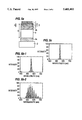
FIG. 1(a) is a sectional view of a light-excited luminescent device having a double resonance structure according to the present invention, and FIG. 1(b) is a graph of the luminescent spectra obtained thereby;
FIG. 2(a) is a sectional view of the light-excited luminescent device and FIG. 2(b) is a graph of the luminescent spectra obtained thereby;
FIG. 3(a) is a sectional view of a light-excited luminescent device having a resonance structure, and FIG. 3(b) is a graph of the luminescent spectra obtained thereby;
FIG. 4(a) is a sectional view illustrating another light-excited luminescent device having a resonance structure, and FIG. 4(b) is a graph of the luminescent spectra obtained thereby;
FIG. 5(a) is a sectional view of an organic EL device having a double resonance structure, FIG. 5(b-1) is a graph of the luminescent spectra obtained by a first resonator and FIG. 5(b-2) is a graph of the luminescent spectra obtained by a second resonator in the device of FIG. 5(a), and FIG. 5(c) is a graph of the combined luminescent spectra of FIGS. 5(b-1) and 5(b-2);
FIG. 6(a) is a sectional view of another organic EL device having a double resonance structure, and FIGS. 6(b-1) to 6(b-3) are graphs of the luminescent spectra produced by the device of FIG. 6(a) when the applied voltage is changed;
FIG. 7 is a diagram illustrating an optical communication device using the organic EL device having a double resonance structure;
FIG. 8 is a diagram illustrating another optical communication device using the organic EL device having a double resonance structure; and
FIG. 9 is a diagram illustrating a display using the organic EL devices having a double resonance structure.
First of all a principle of when a light-excited luminescent device is provided with a resonance function will be described.
FIG. 2(a) illustrates a conventional organic luminescent device having a light-exciting structure.
In this constitution, as shown in FIG. 2(a), a luminescent layer 2 of ALQ compound expressed by the following structural formula (1) is formed on a transparent glass substrate 3, and a thin metal layer 1 is formed thereon to form a reflector. ##STR1##
When this device is irradiated with light from an ultraviolet lamp, luminescent spectra are obtained as shown in FIG. 2(b).
FIG. 3(a), illustrates a device of the constitution of FIG. 2(a) to which a resonance function is added, wherein a half-mirror 4 is formed between the glass substrate 3 and the luminescent layer 2 by forming thin films of a titanium oxide and a silicon oxide one upon the other. The device emits light of a wavelength of a characteristic close to the luminescent wavelength of the device
Luminescent spectrum obtained by this constitution are shown in FIG. 3(b), from which the peak of luminescence is observed near the wavelength of 500 nm.
FIG. 4(a) illustrates a luminescent device having a very small resonance structure of FIG. 3(a) but in which a buffer layer 5 is additionally provided between the luminescent layer and the half-mirror. This buffer layer 5 makes it possible to obtain a resonator of a characteristic wavelength which is longer by about ten times than the luminescent wavelength.
FIG. 4(b) shows luminescent spectrum of FIG. 4(a), in which a plurality of peaks are shown in the resonance region. This is due to the fact that the resonator has a long characteristic wavelength, causing intervals between the wavelengths satisfying the resonance conditions to become short. The envelope of peaks is close to the shape of the luminescent spectrum of FIG. 1(b).
FIG. 1(a) illustrates an example of an organic luminescent device having a multiplex resonance function according to the present invention.
The constitution of FIG. 1(a) is such that the present invention is adapted to the light-excited luminescent device shown in FIG. 3(a).
Referring to FIG. 1(a), a first half-mirror 4a comprising five layers of titanium oxide TiO2 (54 nm thick and silicon oxide SiO2 (86 nm thick) is formed on the transparent glass substrate 1, and a transparent film of silicon oxide is formed thereon to a thickness of about 2 pm. Then, a second half-mirror 4b comprising four layers of TiO2 (54 nm thick) and SiO2 (86 nm thick) is formed, on which is further formed, as a luminescent layer, a film of ALQ of the structural formula (1) which is a sublimated and purified product manufactured by Dojin Kagaku Co. to a thickness of 350 nm. There is further formed thereon a reflector of a thin metal film. In this device, the thin metal film is made of indium.
The thus constituted luminescent device was tested by using an ultraviolet lamp for causing luminescence, and the luminescent spectrum is shown in FIG. 1(b), in which a plurality of peaks are shown like those of the luminescent spectrum of FIG. 4(b). The envelope of these peaks are close to the shape of the luminescent spectrum of FIG. 3(c). That is, it is found that the device of this structure has the features of the two emission wavelengths of the structures of FIGS. 3(a) and 4(a).
By employing a double resonance structure as described above, it is possible to fabricate a device that has a combination of characteristics of a plurality of resonators.
FIG. 5(a) illustrates another embodiment of the present invention, in the form of is a sectional view of the device obtained by applying a double resonance structure to an organic EL device.
In FIG. 5(a), TiO2 layers (54 nm thick) and SiO2 layers (86 nm thick) are formed in five layers on the glass substrate 3 to form a half-mirror 4a. On the half-mirror 4a is formed a transparent buffer layer 5 of silicon oxide of a thickness of 2 pm, on which is further formed a transparent electrode 7 of ITO. There is further formed thereon by vacuum evaporation a luminescent layer 2 comprising TAD layer 2-1 (50 nm thick) expressed by a structural formula (2) and the above-mentioned ALQ layer 2-2 (50 nm thick). On the luminescent layer 2 is formed a thin metal layer 1 of indium that serves as an electrode, and the luminescent side of this layer is used as a reflector surface. ##STR2##
The method of producing the device will be described below.
(1) First, the glass substrate 3 is washed.
(2) Next, the TiO2 layer and the SiO2 layer are alternately formed by sputtering to form the half-mirror 4a.
(3) The buffer layer of silicon oxide (SiO2) is formed by sputtering to a thickness of about 2 pm on the half-mirror 4a that is formed.
(4) Next, the TiO2 layer and the SiO2 layer are alternately formed by sputtering to form the half-mirror 4a in the same manner as in the step (2).
(5) Then, the ITO film is formed also by sputtering and is selectively removed by etching to form an electrode pattern.
(6) Thereafter, a thin film of the above-mentioned TAD is formed by vacuum evaporation on the above electrode.
(7) On the thin TAD film is formed a thin film of ALQ by vacuum evaporation.
(8) A predetermined mask pattern is formed on the ALQ film, and a thin indium film is formed thereon by vacuum evaporation.
In the above-mentioned steps, the sputtering is effected by using a sputtering gas of Ar+4% of O2. The gas pressure is 1.3 Pa, the gas flow rate is 10 sccm, the substrate temperature is 40 (cooled with water), the speed of revolution of a sample holder is 4 rpm, the distance between the sample and the target is 50 mm, and the RF power is 2.6 W/cm for TiO2 and 3.9 W/cm for SiO2.
FIG. 5(c) illustrates the emission spectrum of the constitution of FIG. 5(a). Thus, it is possible to obtain light having a sharp peak near a wavelength of 550 nm. This light is obtained according to the principle described above with reference to FIGS. 2(a) to 4(a). That is, from the light emitted from the luminescent layer 2, light having emission spectrum of FIG. 5(b-1) is obtained by the first resonator A, and the light having emission spectrum of FIG. 5(b-2) is obtained by the resonator B. Emission spectrum of FIG. 5(c) are obtained by combining the above spectra.
By changing the thicknesses of the films according to the present invention, it is possible to obtain emission spectrum having any specific wavelengths. Thus, it is possible to provide a luminescent device with an increased degree of freedom of design.
In the above described embodiments, the a device is designed to emit light having a sharp peak in the direction perpendicular to the layers. The device, however, may be so designed that the light is emitted in an oblique direction with respect to the layers. In this case, the emission spectrum can be varied depending upon the angle of measurement from the front side according to whether or not the average refractive indexes of the first resonator A and the second resonator B are brought into agreement. Even in the embodiments, a similar luminescence could be confirmed even in an oblique direction.
The organic luminescent resonator can be so fabricated that the peak wavelength in the emission spectrum is nearly the same as the wavelength of luminescence, but has a margin in the thickness of the layers which is too small to incorporate a device having another function. Therefore, the effect of realizing a device having a combination of the functions of the two devices by use of the above structure is great.
It should be obvious that the organic luminescent device may have luminescent layers formed by using well-known organic luminescent materials in addition to the structure of the luminescent layers of the above embodiments. The devices also can be fabricated by coating other, rather than evaporation.
Moreover, the above-mentioned embodiments employ a total reflection mirror and two half-reflectors (half-mirrors) to realize a double resonance structure. Depending upon the objects, however, the number of half-mirrors may be increased to obtain a multiplex resonance structure.
FIG. 6(a) is a sectional view of a luminescent device according to another embodiment of the present invention.
In this embodiment, provision is made of a transparent electrode layer 6a of ITO, a liquid crystal layer 8 of polymer dispersion type, and a transparent electrode layer 6b of ITO, instead of the transparent layer 5 of silicon oxide as used in the embodiment of FIG. 5(a). The refractive index is changed by controlling the voltage applied to the liquid crystal layer 8. According to this constitution, the optical distance is varied between the two half-mirrors.
FIGS. 6(b-1) to 6(b-3) illustrate emission spectra when the voltage applied to the liquid crystal layer 8 is changed.
FIG. 6(b-1) shows the emission spectrum when a predetermined voltage is applied. In this case, an emission peak occurs at a wavelength of 600 nm. As the applied voltage is raised, the emission peak will almost disappear, as shown in FIG. 6(b-2). The reason is because the emission wavelengths generated by the first resonator A and the second resonator B do not overlap one upon the other any longer, as if no light was emitted. As the characteristics of the resonator B change causing a further increase in the applied voltage, light of about 480 nm is emitted as shown in FIG. 6(b-3).
The field to which the device of the invention can be applied can be selected according to the emission peak by controlling the voltage.
In this embodiment, the apparent distance of the resonator is varied by providing the liquid crystal layer and the electrode layer for driving the liquid crystal layer. In addition to the above-mentioned constitution, however, it is also possible to employ electromagnetic waves, pressure, temperature or magnetic force to vary the apparent optical length.
Though the above-mentioned embodiment uses the transparent substrate 3, it is also possible to utilize the light of the surface opposite to the substrate by using a half-mirror for the thin metal layer 1, which is the uppermost layer. When the light in the lateral direction is to be utilized, there may be employed an opaque substrate. When the light in the lateral direction is utilized, it becomes essential that at least one of the three reflectors is a semi-transparent one.
As the semi-transparent reflector film, there can be used a dielectric multilayer film, a semitransparent metal film, or a total-reflection film having partly transmitting windows.
FIG. 7 illustrates an example in which the luminescent device of the present invention is applied to optical communication.
In FIG. 7, an organic luminescent device 11 that was described above as a light-emitting device is provided at an end of an optical waveguide 10, the data input from an external unit is subjected to A/D conversion and converted into light signals having different wavelengths depending upon the digital data that is converted, and the light signals are output to the optical waveguide. Light-receiving conversion devices 13 are provided along the optical waveguide or at the other end thereof to receive light signals transmitted through the waveguide. In FIG. 7, the light-receiving conversion devices 13 are so provided along the path of the waveguide as to receive light signals of different wavelengths. This constitution makes it possible to simultaneously transmit large amounts of communication data to different receivers.
FIG. 8 illustrates another example in which the luminescent devices of the present invention are applied to optical communication.
In this embodiment, the optical waveguide 10 is provided with a plurality of organic luminescent devices 11 for transmission to simultaneously emit a plurality of light signals having different wavelengths which are then received by a plurality of light-receiving conversion devices 13 provided along the path of the optical waveguide. Here, any one or all of the plurality of light-receiving conversion devices 13 may be light-receiving conversion devices made up of light-receiving devices capable of receiving light of all the wavelengths, so that all of the data can be transmitted to particular receivers.
FIG. 9 illustrates an embodiment where the luminescent devices of the constitution shown in FIG. 6(a) are applied to a display panel.
The luminescent devices are arranged on the glass substrate in the form of a matrix in units of a pixel. As shown in FIG. 9, the half-mirrors 4a are disposed in the form of a matrix on the glass substrate 3, and transparent electrodes 6a are formed thereon for each column of pixels. Then, a liquid crystal layer is formed thereon to vary the optical length, and transparent electrodes 6b are formed thereon for each row of pixels. Half-mirrors 4b are superposed thereon, and transparent electrodes 7 of ITO are provided on the half-mirrors 4b for each column of pixels. A thin TAD film 2-2 and a thin ALQ film 2-1 are formed on the transparent electrodes 7 to constitute luminescent portions, and metal electrodes 1 are formed for each row of pixels. The surfaces of the metal electrodes in contact with the thin ALQ film 2-1 are so formed as to serve as total reflection surfaces.
The device of this constitution operates as described below.
A voltage is applied between the transparent electrodes 1 and 7 according to the image data to be displayed, so that luminescent devices of predetermined pixels emit light. The luminescent intensity at this moment can be varied in multiple gradations by controlling the voltage that is applied. As for the emission wavelength related to the color of emission, furthermore, the voltage applied between the transparent electrodes 6a and 6b is controlled to change the optical path length of light emitted by the luminescent devices between the half- mirrors 4a, 4b constituting the reflectors and the metal electrodes 1 which are the reflectors, in order to output light of a predetermined color and wavelength.
This makes it possible to eliminate color filters that have been so far necessary and to form a vivid image.
According to the present invention, a single luminescent device makes it possible to obtain an emission spectrum of a combination of characteristics of a plurality of luminescent devices. It is further possible to obtain characteristics such as angle dependence. Moreover, since the freedom of selecting the film thicknesses is ensured, it is possible to realize a device in which a separate function is added to the resonator. By employing the luminescent device for communication, furthermore, it is possible to simultaneously transmit a large quantity of data to different receivers. By applying the luminescent devices to a display for displaying an image, etc., furthermore, it is possible to form a vivid image by means of a simple control operation.
Claims (9)
1. An organic luminescent device with a multiplex structure, comprising: a light-excited luminescent device made up of a substrate, a first half-mirror layer overlying said substrate, an organic luminescent layer, overlying said first half-mirror layer, that emits light, and a reflector overlying said organic luminescent layer, wherein at least one of a buffer layer and a second half-mirror layer is formed between said first half-mirror layer and said organic luminescent layer such that resonators are formed between said reflector and said first half-mirror layer, and between said reflector and any second half-mirror layer.
2. An organic luminescent device with a multiplex structure, comprising: a luminescent device made up of a substrate, a first half-mirror layer overlying said substrate, an electrode layer overlying said first half-mirror layer, an organic luminescent layer, overlying said electrode layer, that emits light, and a metal layer, serving as both a reflector and an electrode, overlying said organic luminescent layer, wherein at least one of a buffer layer and a second half-mirror layer is formed between said first half-mirror layer and said organic luminescent layer such that resonators are formed between said reflector and said first half-mirror layer, and between said reflector and any second half-mirror layer.
3. An organic luminescent device with a multiplex structure, comprising: a substrate, a first half-mirror overlying said substrate, a transparent buffer layer overlying said first half-mirror, a second half-mirror overlying said buffer layer, an organic luminescent layer, that emits light when irradiated with light, overlying said second half-mirror, and a metal layer, serving as a reflector, overlying said organic luminescent layer, wherein a first resonator is provided between said reflector and said second half-mirror, and a second resonator is provided between said reflector and said first half-mirror.
4. An organic luminescent device with a multiplex structure, comprising: a substrate, a first half-mirror overlying said substrate, a transparent buffer layer overlying said first half-mirror, a second half-mirror overlying said transparent buffer layer, a transparent electrode overlying said second half-mirror, an organic luminescent layer, that emits light, overlying said transparent electrode, and a metal layer, serving as a reflector and an electrode, overlying said organic luminescent layer, wherein a first resonator is provided between the reflector of said metal layer and said second half-mirror, and a second resonator is provided between said reflector and said first half-mirror.
5. An organic luminescent device with a multiplex structure according to claim 1 or 2, including both said buffer layer and said second half-mirror layer, said buffer layer being sandwiched between the first half-mirror layer and the second half-mirror layer and the organic luminescent layer overlying the second half-mirror layer, resonators respectively being formed between said reflector and the first half-mirror layer, and between said reflector and the second half-mirror layer.
6. An organic luminescent device with a multiplex structure according to claim 1 or 2, including said second half-mirror layer, between said organic luminescent layer and said first half-mirror layer, such that resonators are respectively provided between said reflector and said first half-mirror layer, and between said reflector and said second half-mirror layer.
7. An organic luminescent device with a multiplex structure according to any one of claims 1, 2, 3 and 4, wherein said substrate is a transparent substrate.
8. An organic luminescent device with a multiplex structure according to claim 3 or 4, wherein said buffer layer varies an optical path length of light emitted by the organic luminescent layer response to signals from an external unit.
9. An organic luminescent device with a multiplex structure according to claim 8, wherein said buffer layer includes a sandwich of a layer of liquid crystal between transparent electrodes, provided between the first half-mirror and the second half-mirror.
Applications Claiming Priority (2)
| Application Number | Priority Date | Filing Date | Title |
|---|---|---|---|
| JP170895 | 1995-01-10 | ||
| JP7-001708 | 1995-01-10 |
Publications (1)
| Publication Number | Publication Date |
|---|---|
| US5682402A true US5682402A (en) | 1997-10-28 |
Family
ID=11509057
Family Applications (1)
| Application Number | Title | Priority Date | Filing Date |
|---|---|---|---|
| US08/584,473 Expired - Lifetime US5682402A (en) | 1995-01-10 | 1996-01-11 | Organic luminescent devices with a multiplex structure |
Country Status (1)
| Country | Link |
|---|---|
| US (1) | US5682402A (en) |
Cited By (23)
| Publication number | Priority date | Publication date | Assignee | Title |
|---|---|---|---|---|
| US5881089A (en) * | 1997-05-13 | 1999-03-09 | Lucent Technologies Inc. | Article comprising an organic laser |
| US5932895A (en) * | 1997-05-20 | 1999-08-03 | The Trustees Of Princeton University | Saturated full color stacked organic light emitting devices |
| US5966393A (en) * | 1996-12-13 | 1999-10-12 | The Regents Of The University Of California | Hybrid light-emitting sources for efficient and cost effective white lighting and for full-color applications |
| EP1043780A1 (en) * | 1998-09-04 | 2000-10-11 | Seiko Epson Corporation | Device with optical communication means |
| US6160828A (en) * | 1997-07-18 | 2000-12-12 | The Trustees Of Princeton University | Organic vertical-cavity surface-emitting laser |
| EP1154676A1 (en) * | 1999-11-22 | 2001-11-14 | Sony Corporation | Display device |
| US6498802B1 (en) | 1999-12-02 | 2002-12-24 | Electronics And Telecommunications Research Institute | Organic micro-cavity laser |
| EP1286184A2 (en) * | 2001-08-07 | 2003-02-26 | Konica Corporation | Half mirror film producing method and optical element comprising a half mirror film |
| US20030219058A1 (en) * | 2002-05-23 | 2003-11-27 | Eastman Kodak Company | Organic vertical cavity laser array device |
| US6661445B2 (en) * | 1998-08-31 | 2003-12-09 | Canon Kabushiki Kaisha | Exposure apparatus with an array of light emitting devices |
| EP1403939A1 (en) * | 2002-09-30 | 2004-03-31 | Kabushiki Kaisha Toyota Jidoshokki | Light-emitting device, display and lighting unit |
| US20050013336A1 (en) * | 2003-07-18 | 2005-01-20 | Eastman Kodak Company | Organic vertical cavity laser array device with varying pixel sizes |
| US20050083460A1 (en) * | 2001-07-16 | 2005-04-21 | Nippon Sheet Glass Co., Ltd. | Semi-transmitting mirror-possessing substrate, and semi-transmitting type liquid crystal display apparatus |
| US20060077386A1 (en) * | 2002-12-30 | 2006-04-13 | Commissarita A L'energie Atomique | Method for the optical characterisation of materials without using a physical model |
| US20060133437A1 (en) * | 2004-12-21 | 2006-06-22 | Trustees Of Princeton University | Organic injection laser |
| US20080253420A1 (en) * | 2003-07-01 | 2008-10-16 | Semiconductor Energy Laboratory Co., Ltd. | Light-emitting device |
| US20110204342A1 (en) * | 2010-02-24 | 2011-08-25 | Hee-Seong Jeong | Organic light-emitting display device and method of manufacturing the same |
| US20110207254A1 (en) * | 2010-02-25 | 2011-08-25 | Lee Joo-Hyeon | Method of manufacturing organic light emitting display device |
| US20110317429A1 (en) * | 2009-03-03 | 2011-12-29 | Satoshi Aiba | Method for producing light-emitting display device, light-emitting display device and light-emitting display |
| USRE43759E1 (en) | 1999-06-02 | 2012-10-23 | Seiko Epson Corporation | Multiple wavelength light emitting device, electronic apparatus, and interference mirror |
| CN103178084A (en) * | 2011-12-23 | 2013-06-26 | 乐金显示有限公司 | Organic light emitting display device |
| JP2017521673A (en) * | 2014-07-25 | 2017-08-03 | フラウンホーファー−ゲゼルシャフト ツゥア フェアデルング デア アンゲヴァンドテン フォァシュング エー.ファウ. | Device for spatially and wavelength-resolved detection of light radiation emitted from at least one OLED or LED |
| US20190064693A1 (en) * | 2015-11-18 | 2019-02-28 | S-Printing Solution Co., Ltd. | Image forming apparatus and light emitting device |
Citations (3)
| Publication number | Priority date | Publication date | Assignee | Title |
|---|---|---|---|---|
| US5307186A (en) * | 1991-08-09 | 1994-04-26 | Sharp Kabushiki Kaisha | Liquid crystal light valve having capability of providing high-contrast image |
| US5369657A (en) * | 1992-09-15 | 1994-11-29 | Texas Instruments Incorporated | Silicon-based microlaser by doped thin films |
| US5384795A (en) * | 1992-09-15 | 1995-01-24 | Texas Instruments Incorporated | Light emission from rare-earth element-doped CaF2 thin films by electroluminescence |
-
1996
- 1996-01-11 US US08/584,473 patent/US5682402A/en not_active Expired - Lifetime
Patent Citations (3)
| Publication number | Priority date | Publication date | Assignee | Title |
|---|---|---|---|---|
| US5307186A (en) * | 1991-08-09 | 1994-04-26 | Sharp Kabushiki Kaisha | Liquid crystal light valve having capability of providing high-contrast image |
| US5369657A (en) * | 1992-09-15 | 1994-11-29 | Texas Instruments Incorporated | Silicon-based microlaser by doped thin films |
| US5384795A (en) * | 1992-09-15 | 1995-01-24 | Texas Instruments Incorporated | Light emission from rare-earth element-doped CaF2 thin films by electroluminescence |
Cited By (47)
| Publication number | Priority date | Publication date | Assignee | Title |
|---|---|---|---|---|
| US5966393A (en) * | 1996-12-13 | 1999-10-12 | The Regents Of The University Of California | Hybrid light-emitting sources for efficient and cost effective white lighting and for full-color applications |
| US5881089A (en) * | 1997-05-13 | 1999-03-09 | Lucent Technologies Inc. | Article comprising an organic laser |
| US5932895A (en) * | 1997-05-20 | 1999-08-03 | The Trustees Of Princeton University | Saturated full color stacked organic light emitting devices |
| US6160828A (en) * | 1997-07-18 | 2000-12-12 | The Trustees Of Princeton University | Organic vertical-cavity surface-emitting laser |
| US6661445B2 (en) * | 1998-08-31 | 2003-12-09 | Canon Kabushiki Kaisha | Exposure apparatus with an array of light emitting devices |
| EP1569280A3 (en) * | 1998-09-04 | 2006-06-07 | Seiko Epson Corporation | Device having light transmission means |
| EP1043780A4 (en) * | 1998-09-04 | 2004-11-17 | Seiko Epson Corp | Device with optical communication means |
| US20030026517A1 (en) * | 1998-09-04 | 2003-02-06 | Seiko Epson Corporation | Device having a light transmission device |
| EP1043780A1 (en) * | 1998-09-04 | 2000-10-11 | Seiko Epson Corporation | Device with optical communication means |
| USRE43759E1 (en) | 1999-06-02 | 2012-10-23 | Seiko Epson Corporation | Multiple wavelength light emitting device, electronic apparatus, and interference mirror |
| USRE45442E1 (en) | 1999-06-02 | 2015-03-31 | Seiko Epson Corporation | Multiple wavelength light emitting device, electronic apparatus, and interference mirror |
| USRE44164E1 (en) | 1999-06-02 | 2013-04-23 | Seiko Epson Corporation | Multiple wavelength light emitting device, electronic apparatus, and interference mirror |
| EP1154676A1 (en) * | 1999-11-22 | 2001-11-14 | Sony Corporation | Display device |
| US7710025B2 (en) | 1999-11-22 | 2010-05-04 | Sony Corporation | Display device using an organic electroluminescence device having resonant cavity |
| US20070228943A1 (en) * | 1999-11-22 | 2007-10-04 | Jiro Yamada | Display device |
| EP1154676A4 (en) * | 1999-11-22 | 2008-08-20 | Sony Corp | Display device |
| US6498802B1 (en) | 1999-12-02 | 2002-12-24 | Electronics And Telecommunications Research Institute | Organic micro-cavity laser |
| US20050083460A1 (en) * | 2001-07-16 | 2005-04-21 | Nippon Sheet Glass Co., Ltd. | Semi-transmitting mirror-possessing substrate, and semi-transmitting type liquid crystal display apparatus |
| US6903512B2 (en) | 2001-08-07 | 2005-06-07 | Konica Corporation | Half mirror film producing method and optical element comprising a half mirror film |
| EP1286184A2 (en) * | 2001-08-07 | 2003-02-26 | Konica Corporation | Half mirror film producing method and optical element comprising a half mirror film |
| EP1286184A3 (en) * | 2001-08-07 | 2004-04-28 | Konica Corporation | Half mirror film producing method and optical element comprising a half mirror film |
| US20030146709A1 (en) * | 2001-08-07 | 2003-08-07 | Konica Corporation | Half mirror film producing method and optical element comprising a half mirror film |
| US6728278B2 (en) * | 2002-05-23 | 2004-04-27 | Eastman Kodak Company | Organic vertical cavity laser array device |
| US20030219058A1 (en) * | 2002-05-23 | 2003-11-27 | Eastman Kodak Company | Organic vertical cavity laser array device |
| US20040105047A1 (en) * | 2002-09-30 | 2004-06-03 | Yoshifumi Kato | Light-emitting device, display unit and lighting unit |
| EP1403939A1 (en) * | 2002-09-30 | 2004-03-31 | Kabushiki Kaisha Toyota Jidoshokki | Light-emitting device, display and lighting unit |
| US20060077386A1 (en) * | 2002-12-30 | 2006-04-13 | Commissarita A L'energie Atomique | Method for the optical characterisation of materials without using a physical model |
| US7307723B2 (en) * | 2002-12-30 | 2007-12-11 | Commissariat A L'energie Atomique | Method for the optical characterization of materials without using a physical model |
| US20080253420A1 (en) * | 2003-07-01 | 2008-10-16 | Semiconductor Energy Laboratory Co., Ltd. | Light-emitting device |
| US7812520B2 (en) | 2003-07-01 | 2010-10-12 | Semiconductor Energy Laboratory Co., Ltd. | Full color display based on organic light-emitting device |
| US20050013336A1 (en) * | 2003-07-18 | 2005-01-20 | Eastman Kodak Company | Organic vertical cavity laser array device with varying pixel sizes |
| CN100423390C (en) * | 2003-07-18 | 2008-10-01 | 伊斯曼柯达公司 | Organic vertical cavity laser array device with varying pixel sizes |
| US6928095B2 (en) * | 2003-07-18 | 2005-08-09 | Eastman Kodak Company | Organic vertical cavity laser array device with varying pixel sizes |
| CN100539335C (en) * | 2004-12-21 | 2009-09-09 | 普林斯顿大学理事会 | Organic injection laser |
| US7242703B2 (en) * | 2004-12-21 | 2007-07-10 | The Trustees Of Princeton University | Organic injection laser |
| US20060133437A1 (en) * | 2004-12-21 | 2006-06-22 | Trustees Of Princeton University | Organic injection laser |
| US10135032B2 (en) * | 2009-03-03 | 2018-11-20 | Udc Ireland Limited | Method for producing light-emitting display device, light-emitting display device and light-emitting display |
| US20110317429A1 (en) * | 2009-03-03 | 2011-12-29 | Satoshi Aiba | Method for producing light-emitting display device, light-emitting display device and light-emitting display |
| US20110204342A1 (en) * | 2010-02-24 | 2011-08-25 | Hee-Seong Jeong | Organic light-emitting display device and method of manufacturing the same |
| US8530888B2 (en) | 2010-02-24 | 2013-09-10 | Samsung Display Co., Ltd. | Organic light-emitting display device and method of manufacturing the same |
| US8435810B2 (en) | 2010-02-25 | 2013-05-07 | Samsung Display Co., Ltd. | Method of manufacturing organic light emitting display device |
| US20110207254A1 (en) * | 2010-02-25 | 2011-08-25 | Lee Joo-Hyeon | Method of manufacturing organic light emitting display device |
| CN103178084A (en) * | 2011-12-23 | 2013-06-26 | 乐金显示有限公司 | Organic light emitting display device |
| CN103178084B (en) * | 2011-12-23 | 2015-10-14 | 乐金显示有限公司 | Organic light-emitting display device |
| JP2017521673A (en) * | 2014-07-25 | 2017-08-03 | フラウンホーファー−ゲゼルシャフト ツゥア フェアデルング デア アンゲヴァンドテン フォァシュング エー.ファウ. | Device for spatially and wavelength-resolved detection of light radiation emitted from at least one OLED or LED |
| US20190064693A1 (en) * | 2015-11-18 | 2019-02-28 | S-Printing Solution Co., Ltd. | Image forming apparatus and light emitting device |
| US10642183B2 (en) * | 2015-11-18 | 2020-05-05 | Hewlett-Packard Development Company, L.P. | Image forming apparatus and light emitting device |
Similar Documents
| Publication | Publication Date | Title |
|---|---|---|
| US5682402A (en) | Organic luminescent devices with a multiplex structure | |
| KR101404546B1 (en) | Organic light emitting diode display and method for manufacturing the same | |
| US7019331B2 (en) | Green light-emitting microcavity OLED device using a yellow color filter element | |
| JP3319251B2 (en) | Light emitting device having multiple resonance structure | |
| EP0616488B1 (en) | Light-emitting elements | |
| KR100690568B1 (en) | Multiple-wavelength light emitting device and electronic apparatus | |
| KR101448003B1 (en) | Organic light emitting diode display and method for manufacturing the same | |
| EP0653902B1 (en) | Variable wavelength luminescent device and control method therefor | |
| JP2553696B2 (en) | Multicolor light emitting thin film electroluminescent device | |
| JP4011126B2 (en) | Method for forming thin-film light absorption layer for electroluminescent device and TFEL device | |
| TWI226504B (en) | A structure of an interference display cell | |
| EP1403939B1 (en) | Light-emitting device, display and lighting unit | |
| KR100875559B1 (en) | display | |
| US8659512B2 (en) | Organic light emitting diode display and method for manufacturing the same | |
| KR20090089151A (en) | Organic light emitting diode display and method for manufacturing the same | |
| CN103077954A (en) | Display unit | |
| KR100809931B1 (en) | Organic Electroluminescence Display and Fabricating Method Thereof | |
| KR101458908B1 (en) | Organic light emitting diode display and method for manufacturing the same | |
| CN112582570A (en) | Display module | |
| US6317179B1 (en) | Reflection type display and coloring method thereof | |
| JP2009049003A (en) | Organic el element | |
| JPH04359B2 (en) | ||
| KR20100059447A (en) | Organic light emitting diode display | |
| KR100326464B1 (en) | Electroluminescent display device | |
| TW591244B (en) | Color changeable pixel |
Legal Events
| Date | Code | Title | Description |
|---|---|---|---|
| AS | Assignment |
Owner name: HITACHI, LTD, JAPAN Free format text: ASSIGNMENT OF ASSIGNORS INTEREST;ASSIGNORS:NAKAYAMA, TAKAHIRO;KAKUTA ATSUSHI;REEL/FRAME:008583/0957 Effective date: 19951218 |
|
| STCF | Information on status: patent grant |
Free format text: PATENTED CASE |
|
| FEPP | Fee payment procedure |
Free format text: PAYOR NUMBER ASSIGNED (ORIGINAL EVENT CODE: ASPN); ENTITY STATUS OF PATENT OWNER: LARGE ENTITY |
|
| FPAY | Fee payment |
Year of fee payment: 4 |
|
| FPAY | Fee payment |
Year of fee payment: 8 |
|
| FPAY | Fee payment |
Year of fee payment: 12 |