US5679971A - Semiconductor integrated circuit - Google Patents
Semiconductor integrated circuit Download PDFInfo
- Publication number
- US5679971A US5679971A US08/505,459 US50545995A US5679971A US 5679971 A US5679971 A US 5679971A US 50545995 A US50545995 A US 50545995A US 5679971 A US5679971 A US 5679971A
- Authority
- US
- United States
- Prior art keywords
- circuit
- power supply
- wiring
- mosfet
- semiconductor substrate
- Prior art date
- Legal status (The legal status is an assumption and is not a legal conclusion. Google has not performed a legal analysis and makes no representation as to the accuracy of the status listed.)
- Expired - Lifetime
Links
Images


Classifications
-
- H—ELECTRICITY
- H01—ELECTRIC ELEMENTS
- H01L—SEMICONDUCTOR DEVICES NOT COVERED BY CLASS H10
- H01L23/00—Details of semiconductor or other solid state devices
- H01L23/58—Structural electrical arrangements for semiconductor devices not otherwise provided for, e.g. in combination with batteries
-
- H—ELECTRICITY
- H01—ELECTRIC ELEMENTS
- H01L—SEMICONDUCTOR DEVICES NOT COVERED BY CLASS H10
- H01L27/00—Devices consisting of a plurality of semiconductor or other solid-state components formed in or on a common substrate
- H01L27/02—Devices consisting of a plurality of semiconductor or other solid-state components formed in or on a common substrate including semiconductor components specially adapted for rectifying, oscillating, amplifying or switching and having at least one potential-jump barrier or surface barrier; including integrated passive circuit elements with at least one potential-jump barrier or surface barrier
- H01L27/0203—Particular design considerations for integrated circuits
- H01L27/0248—Particular design considerations for integrated circuits for electrical or thermal protection, e.g. electrostatic discharge [ESD] protection
- H01L27/0251—Particular design considerations for integrated circuits for electrical or thermal protection, e.g. electrostatic discharge [ESD] protection for MOS devices
- H01L27/0255—Particular design considerations for integrated circuits for electrical or thermal protection, e.g. electrostatic discharge [ESD] protection for MOS devices using diodes as protective elements
-
- H—ELECTRICITY
- H01—ELECTRIC ELEMENTS
- H01L—SEMICONDUCTOR DEVICES NOT COVERED BY CLASS H10
- H01L27/00—Devices consisting of a plurality of semiconductor or other solid-state components formed in or on a common substrate
- H01L27/02—Devices consisting of a plurality of semiconductor or other solid-state components formed in or on a common substrate including semiconductor components specially adapted for rectifying, oscillating, amplifying or switching and having at least one potential-jump barrier or surface barrier; including integrated passive circuit elements with at least one potential-jump barrier or surface barrier
- H01L27/0203—Particular design considerations for integrated circuits
- H01L27/0248—Particular design considerations for integrated circuits for electrical or thermal protection, e.g. electrostatic discharge [ESD] protection
- H01L27/0251—Particular design considerations for integrated circuits for electrical or thermal protection, e.g. electrostatic discharge [ESD] protection for MOS devices
- H01L27/0266—Particular design considerations for integrated circuits for electrical or thermal protection, e.g. electrostatic discharge [ESD] protection for MOS devices using field effect transistors as protective elements
-
- H—ELECTRICITY
- H01—ELECTRIC ELEMENTS
- H01L—SEMICONDUCTOR DEVICES NOT COVERED BY CLASS H10
- H01L2924/00—Indexing scheme for arrangements or methods for connecting or disconnecting semiconductor or solid-state bodies as covered by H01L24/00
- H01L2924/0001—Technical content checked by a classifier
- H01L2924/0002—Not covered by any one of groups H01L24/00, H01L24/00 and H01L2224/00
Definitions
- the present invention relates to a semiconductor integrated circuit, and a technology effectively utilizable for a semiconductor integrated circuit having a plurality of electronic circuits each supplied with power from a plurality of power supply terminals.
- the electrostatic breakdown of a semiconductor integrated circuit is caused by electrostatic discharge arising while the semiconductor integrated circuit is handled or after it is mounted on a printed circuit board.
- Such breakdown includes gate oxide film breakdown, junction breakdown, and wiring fusing of a MOSFET (MOSFET is used to refer to an insulated gate field effect transistor in the present application for patent).
- MOSFET MOSFET is used to refer to an insulated gate field effect transistor in the present application for patent.
- a portion which is least resistant to these three main causes determines the electrostatic breakdown voltage of the semiconductor integrated circuit.
- there have heretofore been contrived circuit arrangements against the gate oxide film breakdown so that no voltage exceeding the breakdown voltage is applied directly to the gate oxide film in the semiconductor integrated circuit even when a high voltage is applied thereto.
- a resistor for a signal line is connected between a pad (external terminal) and the interior of the semiconductor integrated circuit, diodes are inserted between the signal line and a power supply and between the signal line and GND, and, for the junction breakdown, the layout pattern in view of the junction area, the contact arrangement and so forth is contrived.
- wiring fusing further, wiring width enlarging method has been employed.
- Japanese Patent Publication No. 36154/1975 discloses the technology of the countermeasure of the aforementioned electrostatic breakdown.
- the present inventors have adopted a system in which when a semiconductor integrated circuit including analog and digital circuits in combination is developed, these circuits are each supplied with power from independent external terminals to prevent switching noise from being introduced from the digital circuit to the analog circuit via the ground potential of the power supply line or circuit.
- the present inventors have encounter a phenomenon that the internal circuit malfunctions when such a semiconductor integrated circuit is subjected to electrostatic breakdown test using a Human Body Model (HBM) method.
- HBM Human Body Model
- FIG. 13A shows an interface between independent power supply terminals (VDD1, VDD2).
- the interface comprises a P-channel output MOSFET Q20, an N-channel output MOSFET Q21, a P-channel input MOSFET Q22, an N-channel input MOSFET Q23, and wiring for use as a signal transmission path for connecting the commonly connected drains of the output MOSFETs Q20, Q21 and the gates of the input MOSFETs Q22, Q23.
- the power supply terminal VDD1 is, for example, for the digital circuit (or analog circuit)
- the power supply terminal VDD2 is for the analog circuit (or digital circuit).
- FIG. 13B is a schematic element structural sectional view of the interface.
- an overvoltage say, 1,000 V
- a reference voltage of VDD2 due to static electricity is applied to the VDD1 while ground potentials GND1 and GND2 of the circuit are open
- the parasitic capacitance C2 between the well NWEL and a substrate P-SUBSTRATE
- an overvoltage is applied to the gate oxide film of the P-channel input MOSFET Q22 and causes the electrostatic breakdown of the film.
- the gate oxide film of the N-channel input MOSFET Q23 also breaks down likewise when an overvoltage with respect to the potential GND2 is applied to the VDD1 in the state that the VDD2 and GND1 are open.
- An object of the present invention is to provide a reliable semiconductor integrated circuit.
- a semiconductor integrated circuit embodying the present invention comprising a plurality of electronic circuits which are provided with interfaces for effecting signal transmission, and supplied with operating voltages from a plurality of independent power supply terminals, unidirectional elements each having a high threshold voltage so that the elements are off in a normal power supply state are provided between the corresponding power supply terminals.
- the input MOSFET of the interface is protected even when a high voltage due to static electricity is applied to power supply terminals while handling the semiconductor integrated circuit because the power supply terminals are discharged by the unidirectional elements.
- a resistor and a diode both for preventing electrostatic breakdown are connected to the gate of the input MOSFET of the interface for transmitting a signal between electronic circuits.
- the gate of the input MOSFET of the interface is prevented from breakdown by the electrostatic breakdown preventive circuit including the resistor and the diode even when a high voltage due to static electricity is applied to power supply terminals while the semiconductor integrated circuit is handled.
- Still another semiconductor integrated circuit embodying the present invention comprises a semiconductor substrate, a first and a second circuit formed on the semiconductor substrate, a first power supply terminal formed on the semiconductor substrate and used for supplying a first operating voltage to the first circuit, a second power supply terminal formed on the semiconductor substrate and used for supplying a second operating voltage to the second circuit, and a protective element formed on the semiconductor substrate between the first and second power supply terminals, wherein the protective element has a threshold voltage higher than the first and second operating voltages.
- Still another semiconductor integrated circuit embodying the present invention comprises a semiconductor substrate, a first and a second circuit formed on the semiconductor substrate, a first power supply terminal formed on the semiconductor substrate and used for supplying a first operating voltage to the first circuit, a second power supply terminal formed on the semiconductor substrate and used for supplying a second operating voltage to the second circuit, first power supply wiring connected to the first power supply terminal and extended in the first circuit, first reference potential wiring extended in the first circuit, second power supply wiring connected to the second power supply terminal and extended in the second circuit, second reference potential wiring extended in the second circuit, a first and a second MOSFET connected in series between the first power supply wiring and first reference potential wiring in the first circuit, a third and a fourth MOSFET connected in series between the second power supply wiring and the second reference potential wiring in the second circuit, and a signal wiring connected to the first, second and fourth MOSFETs and used for transmitting an output signal of the first circuit to the second circuit, wherein the first and second power supply wirings are electrically independent of each other on the semiconductor substrate, and
- Still another semiconductor integrated circuit embodying the present invention comprises a semiconductor substrate, a first and a second circuit formed on the semiconductor substrate, a first power supply terminal formed on the semiconductor substrate and used for supplying a first operating voltage to the first circuit, a second power supply terminal formed on the semiconductor substrate and used for supplying a second operating voltage to the second circuit, first power supply wiring connected to the first power supply terminal and extended in the first circuit, first reference voltage wiring extended in the first circuit, a second power supply wiring connected to the second power supply terminal and extended in the second circuit, second reference potential wiring extended in the second circuit, a first and a second MOSFET connected in series between the first power supply wiring and a first reference potential wiring in the first circuit, a third and a fourth MOSFET connected in series between the second power supply wiring and the second reference potential wiring in the second circuit, and a signal wiring connected to the first, second and fourth MOSFETs and used for transmitting an output signal of the first circuit to the second circuit, wherein the first and second power supply wirings are electrically independent of each other on the
- FIG. 1 is a block diagram of a semiconductor integrated circuit embodying the present invention.
- FIGS. 2A and 2B are schematic structural sectional views of an aluminum parasitic MOSFET of FIG. 1 embodying the present invention.
- FIGS. 3A and 3B are schematic structural sectional views of another parasitic MOSFET embodying the present invention.
- FIGS. 4A and 4B are schematic structural sectional views of still another parasitic MOSFET embodying the present invention.
- FIG. 5 is a circuit diagram of an interface in a semiconductor integrated circuit according to the present invention.
- FIG. 6 is a schematic element structural sectional view of the interface of FIG. 5 according to the present invention.
- FIGS. 7A and 7B are structural views of another interface embodying the present invention.
- FIG. 8 is a circuit diagram of still another interface embodying the present invention.
- FIG. 9 is a circuit diagram of still another interface embodying the present invention.
- FIG. 10 is a circuit diagram of still another interface embodying the present invention.
- FIG. 11 is a circuit diagram of still another interface embodying the present invention.
- FIG. 12 is a block diagram of a portable communication terminal containing a semiconductor integrated circuit according to the present invention.
- FIGS. 13A and 13B are structural views for illustrating problems to be solved by the present invention.
- FIG. 12 is a block diagram of an embodiment of a portable communication terminal containing a semiconductor integrated circuit to which the present invention is applied.
- This portable communication terminal according to the present invention is mainly made up of a voice code section, a phase modulation-demodulation section, a high-frequency section, a microcomputer for controlling the sections and so forth.
- the semiconductor integrated circuit to which the present invention is applied constitutes the phase modulation-demodulation section in the portable communication terminal.
- the portable communication terminal of the embodiment comprises a voice coding-decoding section (hereinafter referred to as voice coding section) 101, a phase modulation-demodulation section 102 and a high-frequency section 103.
- voice coding section hereinafter referred to as voice coding section
- phase modulation-demodulation section 102 and a high-frequency section 103.
- the operation order of these sections 101-103, the activation and deactivation of the circuits are controlled by signals or pulses from a microcomputer 180, a reset signal generating circuit 190 and a clock generating circuit 140.
- power is supplied from regulators 170, 171 to the voice coding section 101, the phase modulation-demodulation section 102 and the high-frequency section 103.
- the independent regulator 171 is used for the high-frequency section 103 in consideration of the burst operation and the like.
- the phase modulation-demodulation section 102 has a mixture of digital and analog circuits, and is formed into one semiconductor integrated circuit.
- a digital section for processing digital signals comprising a phase modulator 120 and a phase demodulator 125
- an analog section for processing analog signals comprising D/A converters 121-1, 121-2 (hereinafter referred to as D/A), filters 122-1, 122-2, an A/D converter 124, a phase/voltage converter 123, and an offset regulating circuit 126.
- the voice encoding section 101 includes a prefilter 111 for suppressing a high-frequency noise component out of the transmitted analog voice signal fed from a microphone 110, an A/D converter 112 for converting the output of the prefilter 111 to a digital signal, a DSP (digital signal processor) 113 for compressing the frequency band of the output of the A/D converter 112 by processing the digital signal or conversely for expanding the band-compressed digital voice signal thus received to the original band width, a D/A converter 114 for converting the output thus band-expanded by the DSP 113 to an analog voice signal, a post-filter 115 for suppressing the high-frequency components contained in the output of the D/A converter 114 and amplifying the output thereof, and a speaker 116 which is driven by the output of the post filter 115.
- a prefilter 111 for suppressing a high-frequency noise component out of the transmitted analog voice signal fed from a microphone 110
- an A/D converter 112 for converting the output of the prefilter
- the phase modulation-demodulation section 102 includes a phase modulator 120 for subjecting the signal output from the DSP 113 to modulation suitable for radio communication, for example, Gaussian Minimum Shift Keying (GMSK) modulation or ⁇ /4-Shift QPSK modulation, D/A converters 121-1, 121-2 for converting the output of the phase modulator 120 to an analog signal, post-filters 122-1, 122-2 for suppressing the high-frequency components contained in the outputs of the post-filters 122-1, 122-2, a phase/voltage converter 123 for conversely detecting the phase shift contained in the received modulation signal and converting the phase shift to voltage, an A/D converter 124 for converting the output of the phase/voltage converter 123 to a digital signal, and a phase demodulator, 125 for demodulating the original fundamental signal component from the output the A/D converter 124.
- An offset regulating circuit 126 is providing for regulating the offset generated between the D/A converters 121-1, 121-2 and the
- a plurality of sets of a phase modulator 120, D/A converters 121-1, 121-2 and post-filters 122-1, 122-2 are parallely provided in accordance with the system configuration to output a positive-phase signal and a negative-phase signal respectively or signals having phases 90° different from each other, that is, signals whose phases are orthogonal to each other.
- the high-frequency section 103 includes an orthogonal modulator 130 for modulating the signals output from the post-filters 122-1, 122-2 with a radio-frequency carrier signal having a frequency of, for example, about 800 MHz to 2 GHz, a high power amplifier 133 for amplifying the output of the orthogonal modulator 130 up to predetermined transmission power and exciting an antenna 132 via a transmission-reception change-over switch 131, and a detector 135 for detecting a desired signal from the output of the antenna 132 and its amplifier 134.
- a radio-frequency carrier signal having a frequency of, for example, about 800 MHz to 2 GHz
- a high power amplifier 133 for amplifying the output of the orthogonal modulator 130 up to predetermined transmission power and exciting an antenna 132 via a transmission-reception change-over switch 131
- a detector 135 for detecting a desired signal from the output of the antenna 132 and its amplifier 134.
- the orthogonal modulator 130 may have, in accordance with the system configuration, a plurality of stages for effecting modulation with a relatively low frequency of, for example, 455 KHz or 90 KHz, and effecting modulation with a radio-frequency carrier signal of a predetermined frequency of about 800 MHz to 2 GHz.
- FIG. 1 is a block diagram of a semiconductor integral circuit embodying the present invention.
- the semiconductor integrated circuit shown in FIG. 1 is a digital/analog mixed LSI and constitutes the phase modulation-demodulation section 102 of FIG. 12.
- a modem LSI for a portable communication terminal of this embodiment of the present invention has the following three independent power supply terminals to avoid noise interference in the analog part from the digital part and a crystal oscillation circuit.
- An analog power supply terminal VA supplies an operating voltage via power supply wiring on a semiconductor substrate to an amplifier 123', a phase/voltage conversion circuit 123, an A/D converter 124, a D/A converter 121, a post filter 122 and an output buffer 122'.
- a digital power supply terminal VD supplies an operating voltage via power supply wiring on the semiconductor substrate to a frequency divider 142, a delay detection circuit 125 and a modulated waveform generating circuit 120.
- a crystal power supply terminal VX supplies an operating voltage to a crystal oscillation circuit 141. In this case, the terminal means a bonding pad.
- grounding terminals for supplying the ground potentials of the circuits are also supplied with ground potentials of the circuits via independent external terminals GA, GD and GX.
- the same operating voltage of 3-5 V is applied to the power supply terminal VA, VD and VX; however, the voltages to be supplied thereto may be different.
- MOSFETs Q 1 -Q 6 are diode-connected between the above different power supply terminals VA, VD, VX in this embodiment. These MOSFETs Q 1 -Q 6 are allowed to have high threshold voltages so that they are not turned on in a normal operating state as will be described later.
- Use is made of, but not necessarily limited to, a thick field insulating film as a gate insulating film, that is, a so-called parasitic MOSFET.
- a MOSFET hereinafter referred to as N-type aluminum parasitic MOSFET in which the gate insulating film is made up of a field insulating film and the gate is made up of an aluminum layer as state above is used.
- the N-type aluminum parasitic MOSFET Q5 when a positive high voltage compared with the analog power supply terminal VA is applied to the digital power supply terminal, the N-type aluminum parasitic MOSFET Q5 is turned on if the applied voltage exceeds the threshold voltage of the N-type aluminum parasitic MOSFET Q5, which causes the analog power supply terminal VA to electrically connect to the digital power supply terminal VD to conduct.
- the N-type aluminum parasitic MOSFET Q3 When a negative high voltage is applied, the N-type aluminum parasitic MOSFET Q3 is turned on, causing the analog power supply terminal VA to electrically connect to the digital power supply terminal VD. Thereby the potential different between the analog power supply terminal VA and the digital power supply terminal VD is canceled, and thus the electrostatic breakdown of the interface between the analog-digital power supplies is avoided.
- the N-type aluminum parasitic MOSFET Q1 When a positive high voltage with respect to the crystal power supply terminal is applied to the analog power supply terminal VA, the N-type aluminum parasitic MOSFET Q1 is turned on, whereas when a negative-electrode high voltage is applied, the N-type aluminum parasitic MOSFET Q2 is turned on, whereby the potential difference between the analog power supply terminal VA and the crystal power supply terminal VX is canceled.
- the N-type aluminum parasitic MOSFET Q2 is turned on, whereas when a negative high voltage is applied, the N-type aluminum parasitic MOSFET Q1 is turned on, whereby the potential difference between the analog power supply terminal VA and the crystal power supply terminal VX is canceled.
- the threshold voltages of the N-type aluminum parasitic MOSFETs Q 1 -Q 6 are thus utilized to cancel the potential difference between the independent power supply terminals which is the main cause of electrostatic breakdown of the interfaces between the independent power supplies, so that electrostatic breakdown of the interfaces is avoided.
- the constitution of the power supply terminal, the grounding terminal and the input-output terminal is not limited as far as a plurality of independent power supplies are provided, and interfaces between the independent power supplies are provided.
- the amplifier 123' constitutes an input buffer included in the input part of the phase/voltage converter 123 not shown in FIG. 12.
- the output buffers 122' are not shown likewise in FIG. 12, they are included in the output parts of the filters 122-1, 122-2. The rest corresponds to that of FIG. 12.
- FIGS. 2A, 2B are schematic structural sectional views of the aluminum parasitic MOSFETs according to the present invention: FIG. 2A shows an N-type aluminum parasitic MOSFET; and FIG. 2B a P-type aluminum parasitic MOSFET.
- N-type aluminum parasitic MOSFET of FIG. 2A an N + source and an N + drain are formed in a P-substrate, and an aluminum gate is formed, using a field insulating film (450-500 nm) 1 and an interlayer insulating film (400-500 nm) 2 as gate insulating films.
- the aluminum gate 3 is connected to a diffusion layer serving as a drain 5, forming a diode-connected FET.
- an N-type well NWEL is formed in the P-substrate, and a P + source 6 and a P + drain 7 are formed in the NWEL, the rest being the same in structure as those of FIG. 2A.
- the threshold voltages of the aluminum parasitic MOSFETs is 12-15 V.
- FIGS. 3A, 3B are schematic structural sectional views of other parasitic MOSFETs according to the present invention: FIG. 3A shows an N-type parasitic MOSFET; and FIG. 3B a P-type parasitic MOSFET.
- the N-type parasitic MOSFET is provided with a gate oxide film 10 (about 400 nm) which is sufficiently thicker than the gate insulating film (20 nm) of an ordinary MOSFET, and formed on the P-substrate between an N + source 8 and an N + drain 9, a polysilicon gate 11 is formed on the gate oxide film 10, and the drain and the gate electrode are connected in the form of a diode by means of aluminum wiring 12.
- a P-type parasitic MOSFET of FIG. 3B an N-type well NWEL is formed in the P-substrate, and the P + source 8 and P + drain 9 are formed in the NWEL, the rest being the same in structure as those of FIG. 3A.
- FIGS. 4A, 4B are schematic structural sectional views of still other parasitic MOSFETs according to the present invention: FIG. 4A shows a P-type parasitic MOSFET; and FIG. 4B an N-type parasitic MOSFET.
- N-type parasitic MOSFET of FIG. 4B an N + source 19 and an N + drain 20 are formed in a P-substrate, a field insulating film (450-500 nm) 1 therebetween is utilized as a gate insulating film, and a polysilicon gate 15 is formed on the gate oxide film.
- Aluminum wiring 16 is used to connect the drain and the gate electrode 15 in the form of a diode.
- the N-type well NWEL is formed in the P-substrate, and the P + source 17 and P + drain 18 are formed in the NWEL, the rest being the same in structure as those of FIG. 4B.
- the P- and N-channel MOSFETs constituting the digital and analog circuits are, unless otherwise specifically described, of ordinary LDD structure (e.g., formed by the technique disclosed in U.S. Pat. No. 4,366,613) and comprise a gate oxide film (20 nm) on the surface of a semiconductor substrate, a polysilicon gate (200 nm), source and drain region comprising high and low concentration layers.
- the threshold voltages of these P- and N-type MOSFETs are about 0.7 V.
- gates are made of aluminum and polysilicon on the field oxide film or the thick gate insulating film.
- the purpose is to set the absolute values of the threshold voltages of the P- and N-type parasitic MOSFETs to serve as clamp MOSs larger than the normal power supply voltage and smaller than the breakdown voltages of the gate insulating films of MOSFETs constituting the digital and analog circuits. Further, that the purpose is to hold the independent power supply during the normal operation by making use of the threshold voltage of the clamp MOS, and to operate the clamp MOS only when a great potential difference due to static electricity or the like is generated. As shown in FIGS. 2A, 2B, 3A, 3B, 4A, 4B, it is necessary for the threshold voltage to be only made greater by increasing the thicknesses of the field and the gate oxide films.
- the P-type parasitic MOSFETs of FIGS. 2A, 2B, 3A, 3B, 4A, 4B are also usable in place of the N-type parasitic MOSFETs of FIG. 1.
- a combination of N- and P-type parasitic MOSFETs may be used likewise.
- FIG. 5 is a circuit diagram of an interface in a semiconductor integrated circuit according to the present invention.
- Each element of FIG. 5 is formed on one semiconductor substrate of single crystal silicon through a known semiconductor integrated circuit technology.
- the power supply voltages VDD1 and VDD2 are each supplied from different power supply terminals.
- the ground potentials GND1 and GND2 of the circuit are supplied from independent external terminals, as described before.
- the ground potentials GND1 and GND2 of the circuit are internally connected together via a parasitic resistor R2 formed in the semiconductor substrate, the semiconductor region or the like.
- a P-channel MOSFET Q10 and an N-channel MOSFET Q11 constitute a CMOS inverter circuit as an interface output circuit; in other words, it is a circuit for generating an output signal fed to an electronic circuit which is operated by the power supply voltage VDD2, out of the electronic circuits operated by the power supply voltage VDD1.
- the MOSFETs Q10 and Q11 constituting such an output circuit are of LDD structure as will be described later.
- a resistor R1 is provided in a signal transmission path to prevent the aforementioned electrostatic breakdown.
- This resistor R1 is constituted of a polysilicon layer or a P- or N-type semiconductor region formed in the semiconductor substrate.
- a P-channel MOSFET Q12 and an N-channel MOSFET Q13 constituting an input circuit are of single drain structure to prevent their electrostatic breakdown.
- the MOSFETs constituting the input interface circuit is of the single drain structure though the other internal circuits are of LLD structure.
- the channel lengths of the MOSFETs are also set greater than the channel lengths of the output MOSFETs Q10 and Q11 or of the MOSFETs of LLD structure forming the other internal circuits, whereby the MOSFETs constituting the input interface circuit is made to withstand higher voltages.
- FIG. 6 is a schematic element structural sectional view of the interface device according to the present invention.
- the P-channel MOSFET Q10 constituting the output circuit is formed in the N-type well region NWEL, whereas the N-channel MOSFET Q11 is formed in the P-type substrate.
- These MOSFETs Q10 and Q11 are of LDD structure and the MOSFETs constituting the internal circuit are also similar in structure to the P-channel MOSFET Q10 and the N-channel MOSFET Q11.
- the P-channel MOSFET Q12 constituting the input circuit is formed in the N-type well region NWEL, whereas the N-channel MOSFET Q13 is formed in the P-type substrate.
- These MOSFETs Q12 and Q13 are of single drain structure so as to withstand higher voltages.
- the grounding lines GND1, GND2 of the circuit are open, and if a high voltage with respect to the power supply voltage VDD2 is applied to the power supply voltage VDD1, the voltage of the signal line to which the resistor R1 is connected by parasitic capacitance rises with a rise in the voltage of VDD1.
- the input MOSFETs Q12 and Q13 a high voltage is relaxed by the resistor R1 and the parasitic capacitor. Since the MOSFET is of single drain structure, the breakdown voltage of the gate oxide film is increased by increasing the withstand voltage against the junction breakdown and the gate length.
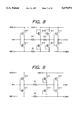
- FIGS. 7A, 7B are block diagrams of another interface embodying the present invention: FIG. 7A shows an example of a circuit; and FIG. 7B a corresponding schematic structural sectional view of the circuit.
- the interface is formed on one semiconductor substrate of single crystal silicon through a known semiconductor integrated circuit technology.
- a P-channel MOSFET Q14 in the form of a diode for clamping voltage is provided between the commonly connected gates of a P-channel MOSFET Q12 and an N-channel MOSFET Q13 constituting the input circuit and the power supply voltage VDD2. Further, a diode-connected N-channel MOSFET Q15 for clamping voltage is provided between the gate and the ground potential GND2. Moreover, a resistor R1 formed with an N + diffusion layer is provided in the signal transmission line for use in transmitting a signal from the output circuit.
- the input MOSFETs Q12, Q13 and the MOSFETs Q14, Q15 for clamping voltage are MOSFETs of single drain structure.
- the GND1, GND2 are open, and if a positive high voltage with respect to the power supply voltage VDD2 is applied to the power supply voltage VDD1, the voltage in the signal transmission path rises with a rise in the voltage of the power supply VDD1. To prevent this, a forward current is made to flow through the protective diode comprising the P-type MOSFET Q14, thereby clamping the voltage of the signal transmission path. Contrarily, when a negative high voltage is applied, the voltage of the signal transmission path lowers with the voltage of the VDD1. To prevent this, by causing a reverse current to flow by use of the breakdown of the protective diode comprising the P-type MOSFET Q14, the voltage of the signal transmission path is clamped.
- the withstand voltage against electrostatic breakdown of the input MOSFETs Q12 and Q13 is improved by means of the protective resistor R1 for suppressing the sharp change of voltage in the signal transmission path and through the operation of the P-type MOSFET Q14 and the N-type MOSFET Q15.
- FIG. 8 is a circuit diagram of still another interface embodying the present invention.
- a further improvement in the withstand voltage against electrostatic breakdown is made by providing R11 and R12 as protective resistors, and two stages of Q14, Q15, and Q16, Q17 as protective diodes which are MOSFETs for clamping voltage. If necessary, similar circuits but of three stages may be provided.
- FIG. 9 is a circuit diagram of still another interface embodying the present invention.
- the N-channel MOSFETs Q14 and Q15 are employed as MOSFETs for clamping voltage in the power supply VDD2 system of the input side.
- the protective diode that has been formed with the P-channel MOSFET Q is formed with an N-channel MOSFET Q.
- the clamping MOSFETs Q14, Q15 and the input MOSFETs Q12, Q13 are of single drain structure.
- the GND1, GND2 are open, and if a positive high voltage with respect to the power supply voltage VDD2 is applied to the power supply voltage VDD1, the voltage in the signal transmission path rises with a rise in the voltage of the power supply VDD1. To prevent this, a forward current is made to flow through the protective diode comprising the N-type MOSFET Q14, thereby clamping the voltage of the signal transmission path. Contrarily, when a negative high voltage is applied, the voltage of the signal transmission path lowers with the voltage of the VDD1. To prevent this, by causing a reverse current to flow by use of the breakdown of the protective diode comprising the N-type MOSFET Q14, the voltage of the signal transmission path is clamped.
- the withstand voltage against electrostatic breakdown of the input MOSFETs Q12 and Q13 is improved by means of the protective resistor R1 for suppressing the sharp change of voltage in the signal transmission path and through the operation of the N-type MOSFET Q14 and the N-channel MOSFET Q15.
- the feature of the interface in this embodiment is the use of only the N-channel MOSFET as a MOSFET for clamping voltage.
- a parasitic bipolar transistor does not constitute a thyristor since no CMOS is used to constitute the MOSFET for clamping voltage of FIG. 7. Consequently, no latch-up is caused by the MOSFET for clamping voltage, and the elements do not need to be spaced apart.
- the layout area can thus be reduced in comparison with a case where the CMOS is employed as shown in FIG. 7.
- FIG. 10 is a circuit diagram of still another interface embodying the present invention.
- N-channel MOSFETs Q14 and Q15 are employed as MOSFETs for clamping voltage in the power supply VDD2 system of the input side.
- the protective diode that has ben formed with the P-channel MOSFET Q is formed with the N-channel MOSFET Q.
- the clamping MOSFETs Q14, Q15 and the input MOSFETs Q12, Q13 are of single drain structure.
- the N-type aluminum parasitic MOSFETs Q16, Q17 are simultaneously used as protective diodes so as to improve the withstand voltage against electrostatic breakdown.
- FIG. 11 is a circuit diagram of still another interface embodying the present invention.
- the power supply voltages are VDD1>VDD2 during the normal operation in this embodiment, the withstand voltage against electrostatic breakdown is improved and the layout area is reduced by connecting the MOSFET for clamping voltage to only the GND2.
- the effect of the embodiment is as follows: (1) In a semiconductor integrated circuit comprising a plurality of electronic circuits which are each provided with an interface for effecting signal transmission, and each supplied with operating voltages from a plurality of independent power supply terminals, protective elements, for example, unidirectional elements having such high threshold voltages that the elements are off in the ordinary state of power supply are provided between the power supply terminals, whereby the input MOSFET of the interface is effectively protected even when a high voltage due to static electricity is applied to each power supply terminal at the time of handling the semiconductor integrated circuit because the power supply terminal is discharged by the protective elements.
- protective elements for example, unidirectional elements having such high threshold voltages that the elements are off in the ordinary state of power supply are provided between the power supply terminals, whereby the input MOSFET of the interface is effectively protected even when a high voltage due to static electricity is applied to each power supply terminal at the time of handling the semiconductor integrated circuit because the power supply terminal is discharged by the protective elements.
- the electronic circuit comprises MOSFETs, and the unidirectional element is a parasitic MOSFET in which the gate insulating film is formed by use of the field insulating film and the gate is connected to the drain. Therefore the unidirectional element is effectively operated only when static electricity is generated without affecting the normal operating condition.
- a semiconductor integrated circuit comprising a plurality of electronic circuits which are each provided with an interface for effecting signal transmission, and each supplied with operating voltages from a plurality of independent power supply terminals, a resistor and a diode both for preventing electrostatic breakdown are connected to the gate of the input MOSFET of the interface for transmitting signals between the electronic circuits.
- independent power supply voltage terminals may be provided so as to avoid noise interference between such electronic circuits as described above. Further, independent power supply voltage terminals may also be provided for each electronic circuit so as to supply different power supply voltages thereto.
- parasitic diodes may be provided between the independent power supply terminals and protective circuit may also be provided in the interfaces. Since a parasitic diode comprising a drain diffusion layer is provided between the power supply line of the output MOSFET of the interface or the grounding line of the circuit and the substrate, any protective circuit is not particularly required when the substrate and the like are floating. However, a high breakdown voltage element may be used if a high voltage is applied therebetween.
- the present invention is widely applicable to various semiconductor integrated circuits having an interface in which a plurality of power supply voltage terminals are provided for some reason, and signals are transferred between electronic circuits supplied with operating voltages through the power supply voltage terminals, like electronic circuits where different power supply voltages are supplied as described above, in addition to digital/analog mixed LSIs as above.
- a semiconductor integrated circuit comprising a plurality of electronic circuits which are each provided with interfaces for effecting signal transmission, and each supplied with operating voltages from the plurality of independent power supply terminals, unidirectional elements each having high threshold voltages at which the elements are off in the ordinary state of power supply are provided between the power supply terminals, whereby the input MOSFET of the interface is effectively protected even when a high voltage due to static electricity is applied to each power supply terminal while handling the semiconductor integrated circuit because power supply terminal is discharged by the unidirectional elements.
- the electronic circuit comprises MOSFETs, and the unidirectional element is a parasitic MOSFET in which the gate insulating film is formed by use of the field insulating film and the gate is connected to the drain. Therefore the unidirectional element is effectively operated only when static electricity is generated without affecting the normal operating condition.
- a resistor and a diode both for preventing electrostatic breakdown are connected to the gate of the input MOSFET of the interface for transmitting signals between the electronic circuits.
Landscapes
- Engineering & Computer Science (AREA)
- Power Engineering (AREA)
- Physics & Mathematics (AREA)
- Condensed Matter Physics & Semiconductors (AREA)
- General Physics & Mathematics (AREA)
- Computer Hardware Design (AREA)
- Microelectronics & Electronic Packaging (AREA)
- Semiconductor Integrated Circuits (AREA)
- Metal-Oxide And Bipolar Metal-Oxide Semiconductor Integrated Circuits (AREA)
Abstract
Description
Claims (9)
Applications Claiming Priority (2)
| Application Number | Priority Date | Filing Date | Title |
|---|---|---|---|
| JP6-191010 | 1994-07-21 | ||
| JP6191010A JPH0837238A (en) | 1994-07-21 | 1994-07-21 | Semiconductor integrated circuit device |
Publications (1)
| Publication Number | Publication Date |
|---|---|
| US5679971A true US5679971A (en) | 1997-10-21 |
Family
ID=16267380
Family Applications (1)
| Application Number | Title | Priority Date | Filing Date |
|---|---|---|---|
| US08/505,459 Expired - Lifetime US5679971A (en) | 1994-07-21 | 1995-07-21 | Semiconductor integrated circuit |
Country Status (4)
| Country | Link |
|---|---|
| US (1) | US5679971A (en) |
| JP (1) | JPH0837238A (en) |
| KR (1) | KR960005986A (en) |
| CN (1) | CN1104743C (en) |
Cited By (24)
| Publication number | Priority date | Publication date | Assignee | Title |
|---|---|---|---|---|
| US5866934A (en) * | 1997-06-20 | 1999-02-02 | Advanced Micro Devices, Inc. | Parallel and series-coupled transistors having gate conductors formed on sidewall surfaces of a sacrificial structure |
| US5905287A (en) * | 1996-04-25 | 1999-05-18 | Nec Corporation | Semiconductor device with high voltage protection |
| US5950091A (en) * | 1996-12-06 | 1999-09-07 | Advanced Micro Devices, Inc. | Method of making a polysilicon gate conductor of an integrated circuit formed as a sidewall spacer on a sacrificial material |
| EP0940852A2 (en) * | 1998-03-04 | 1999-09-08 | Fujitsu Limited | Electrostatic discharge protection for integrated circuit semiconductor device |
| US6049702A (en) * | 1997-12-04 | 2000-04-11 | Rockwell Science Center, Llc | Integrated passive transceiver section |
| WO2000028594A1 (en) * | 1998-11-09 | 2000-05-18 | Koninklijke Philips Electronics N.V. | Over-voltage protection for integrated analog and digital circuits |
| US6124174A (en) * | 1997-05-16 | 2000-09-26 | Advanced Micro Devices, Inc. | Spacer structure as transistor gate |
| US6140682A (en) * | 1999-07-09 | 2000-10-31 | Macronix International Co., Ltd. | Self protected stacked NMOS with non-silicided region to protect mixed-voltage I/O pad from ESD damage |
| US6157530A (en) * | 1999-01-04 | 2000-12-05 | International Business Machines Corporation | Method and apparatus for providing ESD protection |
| US6166415A (en) * | 1998-11-02 | 2000-12-26 | Mitsubishi Denki Kabushiki Kaisha | Semiconductor device with improved noise resistivity |
| US20010025963A1 (en) * | 2000-03-15 | 2001-10-04 | Yoshiyasu Tashiro | Semiconductor device and the process of manufacturing the semiconductor device |
| US6459124B1 (en) * | 1996-10-02 | 2002-10-01 | Semiconductor Energy Laboratory Co., Ltd. | Semiconductor device and process for manufacturing the same, and electronic device |
| US20030067040A1 (en) * | 2001-10-08 | 2003-04-10 | Winbond Electronics Corp. | ESD protection devices and methods to reduce trigger voltage |
| US6636402B1 (en) | 1999-07-24 | 2003-10-21 | Motorola, Inc. | High voltage protection circuit |
| US6858520B2 (en) * | 1994-12-19 | 2005-02-22 | Seiko Instruments Inc. | Method of manufacturing semiconductor device |
| US20060114047A1 (en) * | 2004-11-26 | 2006-06-01 | Nec Electronics Corporation | Semiconductor unit |
| US20060262472A1 (en) * | 2005-05-18 | 2006-11-23 | Nec Electronics Corporation | Semiconductor integrated circuit device |
| US20060273825A1 (en) * | 1997-12-26 | 2006-12-07 | Kazuo Tanaka | Level conversion circuit and semiconductor integrated circuit device employing the level conversion circuit |
| EP1905073A1 (en) * | 2005-06-24 | 2008-04-02 | Semiconductor Energy Laboratory Co., Ltd. | Semiconductor device and wireless communication system |
| US20080218920A1 (en) * | 2007-03-08 | 2008-09-11 | Sarnoff Corporation | Method and aparatus for improved electrostatic discharge protection |
| US20100133616A1 (en) * | 2007-02-22 | 2010-06-03 | Frank David J | Methods of forming wiring to transistor and related transistor |
| US20110255200A1 (en) * | 2010-04-19 | 2011-10-20 | Fu-Yi Tsai | Electrostatic discharge circuit for integrated circuit with multiple power domain |
| US20130170080A1 (en) * | 2011-12-29 | 2013-07-04 | Taiwan Semiconductor Manufacturing Co., Ltd. | Esd protection circuit cell |
| CN101938118B (en) * | 2009-06-29 | 2013-09-04 | 智原科技股份有限公司 | Electrostatic discharge protection circuit with multi-power area integrated circuit |
Families Citing this family (8)
| Publication number | Priority date | Publication date | Assignee | Title |
|---|---|---|---|---|
| JP5070189B2 (en) * | 1998-08-25 | 2012-11-07 | シャープ株式会社 | Static protection device for semiconductor integrated circuit, manufacturing method thereof, and static protection circuit using electrostatic protection device |
| TW473983B (en) | 1999-07-28 | 2002-01-21 | Rohm Co Ltd | Semiconductor integrated circuit device |
| US6566201B1 (en) * | 2001-12-31 | 2003-05-20 | General Semiconductor, Inc. | Method for fabricating a high voltage power MOSFET having a voltage sustaining region that includes doped columns formed by rapid diffusion |
| JP4128091B2 (en) * | 2003-02-20 | 2008-07-30 | 三洋電機株式会社 | Switch circuit device |
| JP4327113B2 (en) * | 2005-02-25 | 2009-09-09 | Okiセミコンダクタ株式会社 | Interface between different power sources and semiconductor integrated circuit |
| JP2010515276A (en) * | 2006-12-31 | 2010-05-06 | サンディスク コーポレイション | System, circuit, chip and method having protection at power island boundaries |
| CN102437563A (en) * | 2011-12-20 | 2012-05-02 | 上海丽恒光微电子科技有限公司 | Single-power circuit and multi-power circuit |
| CN104753517B (en) * | 2013-12-30 | 2018-08-10 | 中芯国际集成电路制造(上海)有限公司 | Signal receiving circuit |
Citations (5)
| Publication number | Priority date | Publication date | Assignee | Title |
|---|---|---|---|---|
| JPS5036154A (en) * | 1973-07-25 | 1975-04-05 | ||
| JPH0468575A (en) * | 1990-07-09 | 1992-03-04 | Sharp Corp | Electrostatic breakdown protective element of semiconductor integrated circuit |
| JPH0494568A (en) * | 1990-08-10 | 1992-03-26 | Nec Ic Microcomput Syst Ltd | Semiconductor integrated circuit |
| US5426323A (en) * | 1993-05-04 | 1995-06-20 | Siemens Aktiengesellschaft | Integrated semiconductor circuit with ESD protection |
| US5514893A (en) * | 1992-01-05 | 1996-05-07 | Matsushita Electric Industrial Co., Ltd. | Semiconductor device for protecting an internal circuit from electrostatic damage |
-
1994
- 1994-07-21 JP JP6191010A patent/JPH0837238A/en active Pending
-
1995
- 1995-07-19 KR KR1019950021180A patent/KR960005986A/en not_active Application Discontinuation
- 1995-07-20 CN CN95109627A patent/CN1104743C/en not_active Expired - Fee Related
- 1995-07-21 US US08/505,459 patent/US5679971A/en not_active Expired - Lifetime
Patent Citations (5)
| Publication number | Priority date | Publication date | Assignee | Title |
|---|---|---|---|---|
| JPS5036154A (en) * | 1973-07-25 | 1975-04-05 | ||
| JPH0468575A (en) * | 1990-07-09 | 1992-03-04 | Sharp Corp | Electrostatic breakdown protective element of semiconductor integrated circuit |
| JPH0494568A (en) * | 1990-08-10 | 1992-03-26 | Nec Ic Microcomput Syst Ltd | Semiconductor integrated circuit |
| US5514893A (en) * | 1992-01-05 | 1996-05-07 | Matsushita Electric Industrial Co., Ltd. | Semiconductor device for protecting an internal circuit from electrostatic damage |
| US5426323A (en) * | 1993-05-04 | 1995-06-20 | Siemens Aktiengesellschaft | Integrated semiconductor circuit with ESD protection |
Non-Patent Citations (2)
| Title |
|---|
| Kalter, "Semiconductor Chip Pad Protect Device" IBM TDB vol. 15 No. 12, May 1973, pp. 3753-3754. |
| Kalter, Semiconductor Chip Pad Protect Device IBM TDB vol. 15 No. 12, May 1973, pp. 3753 3754. * |
Cited By (49)
| Publication number | Priority date | Publication date | Assignee | Title |
|---|---|---|---|---|
| US6858520B2 (en) * | 1994-12-19 | 2005-02-22 | Seiko Instruments Inc. | Method of manufacturing semiconductor device |
| US5905287A (en) * | 1996-04-25 | 1999-05-18 | Nec Corporation | Semiconductor device with high voltage protection |
| US6459124B1 (en) * | 1996-10-02 | 2002-10-01 | Semiconductor Energy Laboratory Co., Ltd. | Semiconductor device and process for manufacturing the same, and electronic device |
| US5950091A (en) * | 1996-12-06 | 1999-09-07 | Advanced Micro Devices, Inc. | Method of making a polysilicon gate conductor of an integrated circuit formed as a sidewall spacer on a sacrificial material |
| US6124174A (en) * | 1997-05-16 | 2000-09-26 | Advanced Micro Devices, Inc. | Spacer structure as transistor gate |
| US5866934A (en) * | 1997-06-20 | 1999-02-02 | Advanced Micro Devices, Inc. | Parallel and series-coupled transistors having gate conductors formed on sidewall surfaces of a sacrificial structure |
| US6383872B1 (en) | 1997-06-20 | 2002-05-07 | Advanced Micro Devices, Inc. | Parallel and series-coupled transistors having gate conductors formed on sidewall surfaces of a sacrificial structure |
| US6049702A (en) * | 1997-12-04 | 2000-04-11 | Rockwell Science Center, Llc | Integrated passive transceiver section |
| US20080266731A1 (en) * | 1997-12-26 | 2008-10-30 | Kazuo Tanaka | Level conversion circuit and semiconductor integrated circuit device employing the level conversion circuit |
| US20110199708A1 (en) * | 1997-12-26 | 2011-08-18 | Renesas Electronics Corporation | Level conversion circuit and semiconductor integrated circuit device employing the level conversion circuit |
| US7403361B2 (en) | 1997-12-26 | 2008-07-22 | Renesas Technology | Level conversion circuit and semiconductor integrated circuit device employing the level conversion circuit |
| US7944656B2 (en) | 1997-12-26 | 2011-05-17 | Renesas Electronics Corporation | Level conversion circuit and semiconductor integrated circuit device employing the level conversion circuit |
| US8139332B2 (en) | 1997-12-26 | 2012-03-20 | Renesas Electronics Corporation | Level conversion circuit and semiconductor integrated circuit device employing the level conversion circuit |
| US8674745B2 (en) | 1997-12-26 | 2014-03-18 | Renesas Electronics Corporation | Level conversion circuit and semiconductor integrated circuit device employing the level conversion circuit |
| US20060273825A1 (en) * | 1997-12-26 | 2006-12-07 | Kazuo Tanaka | Level conversion circuit and semiconductor integrated circuit device employing the level conversion circuit |
| EP0940852A2 (en) * | 1998-03-04 | 1999-09-08 | Fujitsu Limited | Electrostatic discharge protection for integrated circuit semiconductor device |
| US6317305B1 (en) | 1998-03-04 | 2001-11-13 | Fujitsu Limited | Electrostatic discharge protection in semiconductor devices with reduced parasitic capacitance |
| EP0940852A3 (en) * | 1998-03-04 | 2000-11-02 | Fujitsu Microelectronics Europe GmbH | Electrostatic discharge protection for integrated circuit semiconductor device |
| GB2335076B (en) * | 1998-03-04 | 2003-07-16 | Fujitsu Ltd | Electrostatic discharge protection in semiconductor devices |
| US6166415A (en) * | 1998-11-02 | 2000-12-26 | Mitsubishi Denki Kabushiki Kaisha | Semiconductor device with improved noise resistivity |
| WO2000028594A1 (en) * | 1998-11-09 | 2000-05-18 | Koninklijke Philips Electronics N.V. | Over-voltage protection for integrated analog and digital circuits |
| US6292343B1 (en) | 1999-01-04 | 2001-09-18 | International Business Machines Corporation | ASIC book to provide ESD protection on an integrated circuit |
| US6262873B1 (en) | 1999-01-04 | 2001-07-17 | International Business Machines Corporation | Method for providing ESD protection for an integrated circuit |
| US6157530A (en) * | 1999-01-04 | 2000-12-05 | International Business Machines Corporation | Method and apparatus for providing ESD protection |
| US6140682A (en) * | 1999-07-09 | 2000-10-31 | Macronix International Co., Ltd. | Self protected stacked NMOS with non-silicided region to protect mixed-voltage I/O pad from ESD damage |
| US6636402B1 (en) | 1999-07-24 | 2003-10-21 | Motorola, Inc. | High voltage protection circuit |
| KR100698990B1 (en) * | 2000-03-15 | 2007-03-26 | 가부시키가이샤 히타치세이사쿠쇼 | Semiconductor device and the process of manufacturing the semiconductor device |
| US6621108B2 (en) * | 2000-03-15 | 2003-09-16 | Hitachi, Ltd. | Semiconductor device and the process of manufacturing the semiconductor device |
| US20010025963A1 (en) * | 2000-03-15 | 2001-10-04 | Yoshiyasu Tashiro | Semiconductor device and the process of manufacturing the semiconductor device |
| US6858900B2 (en) * | 2001-10-08 | 2005-02-22 | Winbond Electronics Corp | ESD protection devices and methods to reduce trigger voltage |
| US20030067040A1 (en) * | 2001-10-08 | 2003-04-10 | Winbond Electronics Corp. | ESD protection devices and methods to reduce trigger voltage |
| US20060114047A1 (en) * | 2004-11-26 | 2006-06-01 | Nec Electronics Corporation | Semiconductor unit |
| US7495872B2 (en) | 2004-11-26 | 2009-02-24 | Nec Electronics Corporation | Semiconductor unit |
| US20060262472A1 (en) * | 2005-05-18 | 2006-11-23 | Nec Electronics Corporation | Semiconductor integrated circuit device |
| CN100463174C (en) * | 2005-05-18 | 2009-02-18 | 恩益禧电子股份有限公司 | Semiconductor integrated circuit device |
| US7352547B2 (en) * | 2005-05-18 | 2008-04-01 | Nec Electronics Corporation | Semiconductor integrated circuit device |
| EP1905073A1 (en) * | 2005-06-24 | 2008-04-02 | Semiconductor Energy Laboratory Co., Ltd. | Semiconductor device and wireless communication system |
| EP1905073A4 (en) * | 2005-06-24 | 2011-05-11 | Semiconductor Energy Lab | Semiconductor device and wireless communication system |
| US20090255995A1 (en) * | 2005-06-24 | 2009-10-15 | Semiconductor Energy Laboratory Co., Ltd. | Semiconductor device and wireless communication system |
| US20100133616A1 (en) * | 2007-02-22 | 2010-06-03 | Frank David J | Methods of forming wiring to transistor and related transistor |
| US20080218920A1 (en) * | 2007-03-08 | 2008-09-11 | Sarnoff Corporation | Method and aparatus for improved electrostatic discharge protection |
| CN101938118B (en) * | 2009-06-29 | 2013-09-04 | 智原科技股份有限公司 | Electrostatic discharge protection circuit with multi-power area integrated circuit |
| US20110255200A1 (en) * | 2010-04-19 | 2011-10-20 | Fu-Yi Tsai | Electrostatic discharge circuit for integrated circuit with multiple power domain |
| US8339757B2 (en) * | 2010-04-19 | 2012-12-25 | Faraday Technology Corp. | Electrostatic discharge circuit for integrated circuit with multiple power domain |
| US20130170080A1 (en) * | 2011-12-29 | 2013-07-04 | Taiwan Semiconductor Manufacturing Co., Ltd. | Esd protection circuit cell |
| US9069924B2 (en) * | 2011-12-29 | 2015-06-30 | Taiwan Semiconductor Manufacturing Co., Ltd. | ESD protection circuit cell |
| US9893054B2 (en) | 2011-12-29 | 2018-02-13 | Taiwan Semiconductor Manufacturing Co., Ltd. | ESD protection circuit cell |
| US11024625B2 (en) * | 2011-12-29 | 2021-06-01 | Taiwan Semiconductor Manufacturing Co., Ltd. | ESD protection circuit cell |
| US11600613B2 (en) * | 2011-12-29 | 2023-03-07 | Taiwan Semiconductor Manufacturing Co., Ltd. | ESD protection circuit cell |
Also Published As
| Publication number | Publication date |
|---|---|
| KR960005986A (en) | 1996-02-23 |
| JPH0837238A (en) | 1996-02-06 |
| CN1119344A (en) | 1996-03-27 |
| CN1104743C (en) | 2003-04-02 |
Similar Documents
| Publication | Publication Date | Title |
|---|---|---|
| US5679971A (en) | Semiconductor integrated circuit | |
| US6734714B2 (en) | Integrated circuit with closely coupled high voltage output and offline transistor pair | |
| US6515337B1 (en) | Input protection circuit connected to projection circuit power source potential line | |
| US4777518A (en) | Semiconductor device including gate protection circuit with capacitor under input pad | |
| US6978122B2 (en) | High-frequency switching device incorporating an inverter circuit | |
| US5663663A (en) | Mixed voltage interface converter | |
| US7423499B2 (en) | High-frequency switching apparatus | |
| US20030090845A1 (en) | Electrostatic discharge protection for a mixed-voltage device using a stacked-transistor- triggered silicon controlled rectifier | |
| US4811191A (en) | CMOS rectifier circuit | |
| US6049445A (en) | Overvoltage and electrostatic discharge protection for a receiver circuit | |
| TWI254442B (en) | Electrostatic discharge protection circuit | |
| JP4005846B2 (en) | High frequency switch device | |
| US7196379B2 (en) | MOS capacitor device | |
| KR0142001B1 (en) | Mosfet interface circuit having an increased or a reduced mutual conductance | |
| US6822840B2 (en) | Method for protecting MOS components from antenna effect and the apparatus thereof | |
| JP4183980B2 (en) | Semiconductor integrated circuit device | |
| US20040080877A1 (en) | Esd protection circuit for low amplitude signals | |
| JP4285792B2 (en) | Electrostatic breakdown protection circuit in semiconductor integrated circuit device | |
| US6737890B2 (en) | Switching circuit device | |
| JP2970826B2 (en) | Protection circuit built-in IC and display device driving IC | |
| US20020040984A1 (en) | I/O circuit of semiconductor integrated device | |
| US20240120734A1 (en) | Semiconductor die with transformer and esd clamp circuit | |
| EP1701385A1 (en) | Semiconductor device comprising electrostatic breakdown protection element | |
| US20040150045A1 (en) | LSI alleviating hysteresis of delay time | |
| JP2002261593A (en) | Compound semiconductor switching circuit |
Legal Events
| Date | Code | Title | Description |
|---|---|---|---|
| AS | Assignment |
Owner name: HITACHI TOHBU SEMICONDUCTOR, LTD., JAPAN Free format text: ASSIGNMENT OF ASSIGNORS INTEREST;ASSIGNORS:TAMBA, YUKO;NAGATANI, AKIHIRO;OKAZAKI, TAKAO;REEL/FRAME:008438/0885 Effective date: 19950626 Owner name: HITACHI, LTD., JAPAN Free format text: ASSIGNMENT OF ASSIGNORS INTEREST;ASSIGNORS:TAMBA, YUKO;NAGATANI, AKIHIRO;OKAZAKI, TAKAO;REEL/FRAME:008438/0885 Effective date: 19950626 |
|
| STCF | Information on status: patent grant |
Free format text: PATENTED CASE |
|
| FEPP | Fee payment procedure |
Free format text: PAYOR NUMBER ASSIGNED (ORIGINAL EVENT CODE: ASPN); ENTITY STATUS OF PATENT OWNER: LARGE ENTITY |
|
| FPAY | Fee payment |
Year of fee payment: 4 |
|
| FEPP | Fee payment procedure |
Free format text: PAYER NUMBER DE-ASSIGNED (ORIGINAL EVENT CODE: RMPN); ENTITY STATUS OF PATENT OWNER: LARGE ENTITY |
|
| FPAY | Fee payment |
Year of fee payment: 8 |
|
| FEPP | Fee payment procedure |
Free format text: PAYOR NUMBER ASSIGNED (ORIGINAL EVENT CODE: ASPN); ENTITY STATUS OF PATENT OWNER: LARGE ENTITY |
|
| FPAY | Fee payment |
Year of fee payment: 12 |
|
| AS | Assignment |
Owner name: RENESAS ELECTRONICS CORPORATION, JAPAN Free format text: ASSIGNMENT OF ASSIGNORS INTEREST;ASSIGNOR:HITACHI, LTD.;REEL/FRAME:026109/0976 Effective date: 20110307 |