US5658190A - Apparatus for separating wafers from polishing pads used in chemical-mechanical planarization of semiconductor wafers - Google Patents
Apparatus for separating wafers from polishing pads used in chemical-mechanical planarization of semiconductor wafers Download PDFInfo
- Publication number
- US5658190A US5658190A US08/573,430 US57343095A US5658190A US 5658190 A US5658190 A US 5658190A US 57343095 A US57343095 A US 57343095A US 5658190 A US5658190 A US 5658190A
- Authority
- US
- United States
- Prior art keywords
- wafer
- pad
- platen
- carrier
- polishing pad
- Prior art date
- Legal status (The legal status is an assumption and is not a legal conclusion. Google has not performed a legal analysis and makes no representation as to the accuracy of the status listed.)
- Expired - Lifetime
Links
Images


Classifications
-
- B—PERFORMING OPERATIONS; TRANSPORTING
- B24—GRINDING; POLISHING
- B24B—MACHINES, DEVICES, OR PROCESSES FOR GRINDING OR POLISHING; DRESSING OR CONDITIONING OF ABRADING SURFACES; FEEDING OF GRINDING, POLISHING, OR LAPPING AGENTS
- B24B37/00—Lapping machines or devices; Accessories
- B24B37/34—Accessories
- B24B37/345—Feeding, loading or unloading work specially adapted to lapping
-
- Y—GENERAL TAGGING OF NEW TECHNOLOGICAL DEVELOPMENTS; GENERAL TAGGING OF CROSS-SECTIONAL TECHNOLOGIES SPANNING OVER SEVERAL SECTIONS OF THE IPC; TECHNICAL SUBJECTS COVERED BY FORMER USPC CROSS-REFERENCE ART COLLECTIONS [XRACs] AND DIGESTS
- Y10—TECHNICAL SUBJECTS COVERED BY FORMER USPC
- Y10S—TECHNICAL SUBJECTS COVERED BY FORMER USPC CROSS-REFERENCE ART COLLECTIONS [XRACs] AND DIGESTS
- Y10S451/00—Abrading
- Y10S451/921—Pad for lens shaping tool
Definitions
- the present invention relates to chemical-mechanical planarization of semiconductor wafers, and more specifically to a planarizing machine with a separator for separating a planarized wafer from a polishing pad.
- CMP Chemical-mechanical planarization
- a planarizing surface on a polishing pad is covered with a slurry solution containing small, abrasive particles and reactive chemicals.
- a wafer is mounted in a wafer holder, and the wafer holder is positioned opposite the polishing pad.
- the wafer and/or the polishing pad are then moved relative to one another allowing the abrasive particles in the slurry to mechanically remove the surface of the wafer, and the reactive chemicals in the slurry to chemically remove the surface of the wafer.
- CMP processes must consistently and accurately planarize a uniform, planar surface on the wafer at a desired end-point.
- Many microelectronic devices are typically fabricated on a single wafer by depositing layers of various materials on the wafer, and manipulating the wafer and the other layers of material with photolithographic, etching, and doping processes.
- CMP processes In order to manufacture ultra-high density integrated circuits, CMP processes must provide a highly planar surface so that the geometries of the component parts of the circuits may be accurately positioned across the full surface of the wafer.
- Integrated circuits are generally patterned on a wafer by optically or electromagnetically focusing a circuit pattern on the surface of the wafer. If the surface of the wafer is not highly planar, the circuit pattern may not be sufficiently focused in some areas, resulting in defective devices. Therefore, it is important to consistently and accurately create a uniformly planar surface on the wafer.
- polishing pad provides a number of wells in the pad substrate that are uniformly spaced apart from one another across the surface of the pad. Each well holds a volume of slurry, and as the pad passes across the surface of the wafer, the slurry is drawn out of the wells into the space between the wafer and the pad. As the slurry is drawn out of the wells, a vacuum is created in the wells that holds the wafer next to the planarizing surface of the pad.
- CMP processes must also provide a high throughput of finished devices to lower the unit cost of each device.
- the wafers therefore, are generally between six inches and eight inches in diameter so that hundreds of microelectronic devices may be simultaneously fabricated on a single wafer.
- six to eight inch diameter wafers are planarized in the presence of a slurry, however, a significant surface tension exists between the wafer, slurry, and polishing pad that holds the wafers next to the polishing pad.
- CMP planarizers One problem with current CMP planarizers is that after the CMP process is finished, it is difficult to remove large wafers from conventional polishing pads, or any wafer from polishing pads with slurry wells. Wafers are attached to the wafer carrier by drawing a vacuum on the backside of the wafer that is low enough to prevent the wafer from being damaged. After planarizing, wafers are conventionally removed from polishing pads by simply lifting the wafer carrier. Such a low vacuum, however, generally does not provide enough force to overcome the surface bond between large wafers and the polishing pads. Similarly, such low vacuums are also insufficient to overcome the bond between wafers and polishing pads with slurry wells. Therefore, it would be desirable to develop a CMP machine that can separate virtually any type of wafer from any type of polishing pad.
- the inventive machine is a planarizer for use in chemical-mechanical planarization of semiconductor wafers that has a moveable platen, a polishing pad, a wafer carrier, and a wafer separator.
- the polishing pad is positioned on the platen, and it has a planarizing surface with an operational zone upon which the wafer may be planarized.
- the wafer carrier holds a wafer, and it is positionable opposite the polishing pad to engage the wafer with the operational zone of the polishing pad.
- the wafer separator engages either the polishing pad, the wafer, or the wafer carrier to lift a portion of the wafer away from the pad.
- the wafer is held by a wafer carrier and pressed against the polishing pad in the presence of a slurry. At least one of the wafer or the polishing pad is moved with respect to the other to remove material from the surface of the wafer. After a desired mount of material is removed from the surface of the wafer, a portion of the wafer is separated from the pad to break a surface bond between the wafer and the polishing pad.
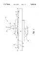
- FIG. 1 is a schematic cross-sectional view of a chemical-mechanical planarization machine in accordance with the invention.
- FIG. 2 is a top elevational view of a chemical-mechanical planarization machine in accordance with the invention.
- FIG. 3 is a partial cross-sectional view of the chemical-mechanical planarization machine of FIG. 1.
- FIG. 4 is a schematic cross-sectional view of another chemical-mechanical planarization machine in accordance with the invention.
- FIG. 5 is a partial cross-sectional view of the chemical-mechanical planarization machine of FIG. 4.
- FIG. 6 is a schematic cross-sectional view of another chemical-mechanical planarization machine in accordance with the invention.
- FIG. 7 is a schematic cross-sectional view of another chemical-mechanical planarization machine in accordance with the invention.
- FIG. 8A is a schematic cross-sectional view of another chemical-mechanical planarization machine in accordance with the invention.
- FIG. 8B is a schematic cross-sectional view of another chemical-mechanical planarization machine in accordance with the invention.
- the present invention provides a chemical-mechanical planarization machine that can separate virtually any type of wafer from any type of polishing pad after the wafer has been planarized.
- Conventional chemical-mechanical planarization machines typically cannot remove large wafers from polishing pads, or most any type of wafer from pads with slurry wells, because the vacuum on the backside of the wafer is insufficient to break the bond between such wafers and polishing pads.
- the present invention provides a wafer separator that acts against only a portion of the wafer, and preferably only a peripheral portion of the wafer. By acting against only a portion of the wafer instead of the whole surface area, a relatively small force can separate the wafer from the polishing pad.
- FIGS. 1-8 in which like reference numbers refer to like parts throughout the various figures.
- FIGS. 1 and 2 illustrate a chemical-mechanical planarization machine 10 with a platen 20, a wafer carrier 30, a polishing pad 40, and a wafer separator 70.
- the platen 20 has a top surface 22 upon which the polishing pad 40 is positioned.
- a drive assembly 26 rotates the platen 20 as indicated by arrow A, and/or reciprocates the platen 20 back and forth as indicated by arrow B. The motion of the platen 20 is imparted to the pad 40 because the polishing pad 40 is adhered to the top surface 22 of the platen 20.
- the wafer carrier 30 has a lower surface 32 to which a wafer 60 may be attached by drawing a vacuum on the backside of the wafer.
- a resilient pad 34 may be positioned between the wafer 60 and the lower surface 32 to enhance the connection between the wafer 60 and the wafer carrier 30.
- the wafer carrier 30 may have an actuator assembly 36 attached to it for imparting axial and/or rotational motion as indicated by arrows C and D, respectively.
- the actuator assembly 36 is generally attached to the wafer carrier 30 by a gimbal joint that allows the wafer carrier 30 to pivot freely about the three orthogonal axes centered at the end of the actuator 36.
- the wafer separator 70 is positioned towards the perimeter of the pad, and it has a contact surface 72 that engages either the pad 40, the wafer 60, or the wafer carrier 30.
- the wafer separator 70 may be passive, in which a peripheral portion of the wafer 60 is urged away from the pad 40 by positioning the pad 40 on the wafer separator 70, or moving the wafer 60 and/or the wafer carrier 30 against the wafer separator 70.
- the wafer separator 70 may be active, in which the wafer separator 70 is moved against one of the pad 40, the wafer 60, or the wafer carrier 30 to separate the wafer 60 from the pad 40.
- the wafer separator 70 has many configurations, including a ring (shown in FIG. 2) that has an upper surface that defines the contact surface 72.
- the wafer separator 70 may alternatively be a number of tapered segments (not shown) positioned about the perimeter of the pad 40.
- the ring may have a wedge-shaped cross-section, a semi-circular shaped cross-section, a semi-elliptical cross-section, or any other suitable cross-section that provides an inclined contact surface that lifts a portion of the wafer 60 from the pad 40.
- the wafer separator 70 may be positioned on the pad, the platen, or separately from the pad and platen.
- the wafer separator 70 is a ring-like ridge positioned on the top surface 22 of the platen 20 towards the perimeter of the platen 20.
- the wafer separator 70 has a wedge-shaped cross-section with an upper surface 72 that defines the contact surface.
- the perimeter of the pad 40 is positioned on the contact surface 72 to form a non-planar section 43 on the pad 40.
- FIG. 3 shows the operation of the embodiment of the wafer separator 70 illustrated in FIGS. 1 and 2.
- the wafer 60 is substantially rigid and cannot conform to the non-planar section 43 of the pad 40.
- a peripheral portion of the bottom surface 62 of the wafer 60 is pried away from the upper surface 42 of the pad 40 to form a gap 80.
- the wafer 60 can be fully separated from the pad 40 by lifting the wafer carrier 30 upwardly in the direction of arrow C (shown in FIG. 1).
- FIG. 4 illustrates another embodiment of the invention, in which the wafer separator 70 is positioned on the upper surface 42 of the polishing pad 40.
- the wafer separator 70 is positioned towards the perimeter of the polishing pad 40 so that it is outside of an operational zone on the pad where the wafer 60 is planarized.
- the wafer carrier 30 and wafer 60 are moved across the pad until at least one of them engages the wafer separator.
- the contact surface 72 engages either a forward edge 31 of the wafer carrier 30 (shown by FIG. 5), or a peripheral portion of the wafer 60 itself (not shown).
- the peripheral portion of the wafer 60 proximate to the forward edge 31 is lifted away from the pad 40.
- the wafer separator 70 engages the wafer 60 (not shown), the peripheral portion of the wafer 60 proximate to the wafer separator 70 is pried from pad 40.
- the wafer separator 70 allows the wafer 60 to be easily removed from the pad 40.
- FIGS. 6 and 7 illustrate additional embodiments of the invention in which the wafer separator 70 is positioned radially outwardly from the perimeter of the platen 20.
- the wafer separator 70 is attached to the platen 20 by an arm 73. While in FIG. 7, the wafer separator 70 is attached to a wall 24 of the planarizer 10.
- the wafer separators 70 illustrated in FIGS. 6 and 7 operate by separating a peripheral portion of the wafer 60 from the pad 40.
- the wafer separators 70 shown in FIGS. 6 and 7 are attached to the platen 20 and the wall 24, respectively, at an elevation that aligns the contact surface 72 with either the wafer 60 or the wafer carrier 30.
- FIGS. 1-7 illustrate a passive wafer separator 70 that operates by positioning the pad 40 on the contact surface 72 of the wafer separator 70, or by moving the wafer 60 and the wafer carrier 30 to engage the contact surface 72.
- the wafer separator 70 may be active such that it can be moved to engage the appropriate item on the planarizer.
- a wafer separator 70 may be attached to an actuator (not shown) that is connected to the wall 24 (shown in FIG. 7) of the planarizer 10.
- the actuator may be extended radially inwardly towards the center of the platen 20 to engage the wafer separator 70 with either the pad 40, the wafer 60, or the wafer carrier 30.
- the present invention therefore, is not limited to passive wafer separators.
- FIG. 8A illustrates another type of active wafer separator 170.
- the active wafer separator 170 is a piston 171 with an extensible rod 172.
- the piston 171 is positioned in a hole 23 towards the perimeter of the platen 20.
- the wafer carrier 30 and wafer 60 are translated across the surface of the pad 40 until the front edge 31 of the wafer carrier 30 is positioned over the rod 172.
- the rod 172 is then engaged with the wafer carrier 30, and the wafer carrier 30 and wafer 60 are lifted from the pad 40.
- FIG. 8B shows another embodiment in which the active wafer separator 170 is attached to the wall 24 of the planarizer 10.
- the wafer carrier 30 and wafer 60 are translated across the surface of the pad 40 and over the peripheral edge of the platen 20.
- the hole 23 may be positioned at or near the center of the pad 40 so that a central portion of the pad may be deformed upwardly to separate any portion of the wafer from the pad.
- the present invention covers separating any portion of the wafer from the pad.
- One advantage of the present invention is that it provides a chemical-mechanical planarizer 10 with a wafer separator that separates virtually any type of wafer from any type of polishing pad.
- the present invention is particularly useful in connection with larger wafers having diameters between 6 and 8 inches, and polishing pads with slurry wells.
- the present invention is not limited to such particular uses and may be useful for smaller wafers as well.
Abstract
Description
Claims (6)
Priority Applications (2)
| Application Number | Priority Date | Filing Date | Title |
|---|---|---|---|
| US08/573,430 US5658190A (en) | 1995-12-15 | 1995-12-15 | Apparatus for separating wafers from polishing pads used in chemical-mechanical planarization of semiconductor wafers |
| US08/910,693 US5882248A (en) | 1995-12-15 | 1997-08-13 | Apparatus for separating wafers from polishing pads used in chemical-mechanical planarization of semiconductor wafers |
Applications Claiming Priority (1)
| Application Number | Priority Date | Filing Date | Title |
|---|---|---|---|
| US08/573,430 US5658190A (en) | 1995-12-15 | 1995-12-15 | Apparatus for separating wafers from polishing pads used in chemical-mechanical planarization of semiconductor wafers |
Related Child Applications (1)
| Application Number | Title | Priority Date | Filing Date |
|---|---|---|---|
| US08/910,693 Continuation US5882248A (en) | 1995-12-15 | 1997-08-13 | Apparatus for separating wafers from polishing pads used in chemical-mechanical planarization of semiconductor wafers |
Publications (1)
| Publication Number | Publication Date |
|---|---|
| US5658190A true US5658190A (en) | 1997-08-19 |
Family
ID=24291965
Family Applications (2)
| Application Number | Title | Priority Date | Filing Date |
|---|---|---|---|
| US08/573,430 Expired - Lifetime US5658190A (en) | 1995-12-15 | 1995-12-15 | Apparatus for separating wafers from polishing pads used in chemical-mechanical planarization of semiconductor wafers |
| US08/910,693 Expired - Lifetime US5882248A (en) | 1995-12-15 | 1997-08-13 | Apparatus for separating wafers from polishing pads used in chemical-mechanical planarization of semiconductor wafers |
Family Applications After (1)
| Application Number | Title | Priority Date | Filing Date |
|---|---|---|---|
| US08/910,693 Expired - Lifetime US5882248A (en) | 1995-12-15 | 1997-08-13 | Apparatus for separating wafers from polishing pads used in chemical-mechanical planarization of semiconductor wafers |
Country Status (1)
| Country | Link |
|---|---|
| US (2) | US5658190A (en) |
Cited By (52)
| Publication number | Priority date | Publication date | Assignee | Title |
|---|---|---|---|---|
| US5879226A (en) * | 1996-05-21 | 1999-03-09 | Micron Technology, Inc. | Method for conditioning a polishing pad used in chemical-mechanical planarization of semiconductor wafers |
| US5882248A (en) * | 1995-12-15 | 1999-03-16 | Micron Technology, Inc. | Apparatus for separating wafers from polishing pads used in chemical-mechanical planarization of semiconductor wafers |
| US6267650B1 (en) * | 1999-08-09 | 2001-07-31 | Micron Technology, Inc. | Apparatus and methods for substantial planarization of solder bumps |
| US6287174B1 (en) | 1999-02-05 | 2001-09-11 | Rodel Holdings Inc. | Polishing pad and method of use thereof |
| US6331135B1 (en) * | 1999-08-31 | 2001-12-18 | Micron Technology, Inc. | Method and apparatus for mechanical and chemical-mechanical planarization of microelectronic substrates with metal compound abrasives |
| US6343978B1 (en) * | 1997-05-16 | 2002-02-05 | Ebara Corporation | Method and apparatus for polishing workpiece |
| US20020069967A1 (en) * | 2000-05-04 | 2002-06-13 | Wright David Q. | Planarizing machines and methods for mechanical and/or chemical-mechanical planarization of microelectronic-device substrate assemblies |
| US6425816B1 (en) * | 1997-04-04 | 2002-07-30 | Rodel Holdings Inc. | Polishing pads and methods relating thereto |
| US6498101B1 (en) | 2000-02-28 | 2002-12-24 | Micron Technology, Inc. | Planarizing pads, planarizing machines and methods for making and using planarizing pads in mechanical and chemical-mechanical planarization of microelectronic device substrate assemblies |
| US6511576B2 (en) | 1999-11-17 | 2003-01-28 | Micron Technology, Inc. | System for planarizing microelectronic substrates having apertures |
| US6520834B1 (en) | 2000-08-09 | 2003-02-18 | Micron Technology, Inc. | Methods and apparatuses for analyzing and controlling performance parameters in mechanical and chemical-mechanical planarization of microelectronic substrates |
| US6533893B2 (en) | 1999-09-02 | 2003-03-18 | Micron Technology, Inc. | Method and apparatus for chemical-mechanical planarization of microelectronic substrates with selected planarizing liquids |
| US20030060128A1 (en) * | 1999-08-31 | 2003-03-27 | Moore Scott E. | Apparatus and method for conditioning and monitoring media used for chemical-mechanical planarization |
| US6548407B1 (en) | 2000-04-26 | 2003-04-15 | Micron Technology, Inc. | Method and apparatus for controlling chemical interactions during planarization of microelectronic substrates |
| US6592443B1 (en) | 2000-08-30 | 2003-07-15 | Micron Technology, Inc. | Method and apparatus for forming and using planarizing pads for mechanical and chemical-mechanical planarization of microelectronic substrates |
| US6623329B1 (en) | 2000-08-31 | 2003-09-23 | Micron Technology, Inc. | Method and apparatus for supporting a microelectronic substrate relative to a planarization pad |
| US6628410B2 (en) | 1996-02-16 | 2003-09-30 | Micron Technology, Inc. | Endpoint detector and method for measuring a change in wafer thickness in chemical-mechanical polishing of semiconductor wafers and other microelectronic substrates |
| US6652764B1 (en) | 2000-08-31 | 2003-11-25 | Micron Technology, Inc. | Methods and apparatuses for making and using planarizing pads for mechanical and chemical-mechanical planarization of microelectronic substrates |
| US6666749B2 (en) | 2001-08-30 | 2003-12-23 | Micron Technology, Inc. | Apparatus and method for enhanced processing of microelectronic workpieces |
| US20040038623A1 (en) * | 2002-08-26 | 2004-02-26 | Nagasubramaniyan Chandrasekaran | Methods and systems for conditioning planarizing pads used in planarizing substrates |
| US20040038534A1 (en) * | 2002-08-21 | 2004-02-26 | Taylor Theodore M. | Apparatus and method for conditioning a polishing pad used for mechanical and/or chemical-mechanical planarization |
| US20040041556A1 (en) * | 2002-08-29 | 2004-03-04 | Martin Michael H. | Planarity diagnostic system, E.G., for microelectronic component test systems |
| US6722943B2 (en) | 2001-08-24 | 2004-04-20 | Micron Technology, Inc. | Planarizing machines and methods for dispensing planarizing solutions in the processing of microelectronic workpieces |
| US6736869B1 (en) | 2000-08-28 | 2004-05-18 | Micron Technology, Inc. | Method for forming a planarizing pad for planarization of microelectronic substrates |
| US6769967B1 (en) | 1996-10-21 | 2004-08-03 | Micron Technology, Inc. | Apparatus and method for refurbishing polishing pads used in chemical-mechanical planarization of semiconductor wafers |
| US6838382B1 (en) | 2000-08-28 | 2005-01-04 | Micron Technology, Inc. | Method and apparatus for forming a planarizing pad having a film and texture elements for planarization of microelectronic substrates |
| US20050014457A1 (en) * | 2001-08-24 | 2005-01-20 | Taylor Theodore M. | Apparatus and method for conditioning a contact surface of a processing pad used in processing microelectronic workpieces |
| US20050026544A1 (en) * | 2003-01-16 | 2005-02-03 | Elledge Jason B. | Carrier assemblies, polishing machines including carrier assemblies, and methods for polishing micro-device workpieces |
| US20050026555A1 (en) * | 2002-08-08 | 2005-02-03 | Terry Castor | Carrier assemblies, planarizing apparatuses including carrier assemblies, and methods for planarizing micro-device workpieces |
| US20050026545A1 (en) * | 2003-03-03 | 2005-02-03 | Elledge Jason B. | Systems and methods for monitoring characteristics of a polishing pad used in polishing micro-device workpieces |
| US20050037694A1 (en) * | 2002-07-08 | 2005-02-17 | Taylor Theodore M. | Retaining rings, planarizing apparatuses including retaining rings, and methods for planarizing micro-device workpieces |
| US6884152B2 (en) | 2003-02-11 | 2005-04-26 | Micron Technology, Inc. | Apparatuses and methods for conditioning polishing pads used in polishing micro-device workpieces |
| US6922253B2 (en) | 2000-08-30 | 2005-07-26 | Micron Technology, Inc. | Planarizing machines and control systems for mechanical and/or chemical-mechanical planarization of microelectronic substrates |
| US6935929B2 (en) | 2003-04-28 | 2005-08-30 | Micron Technology, Inc. | Polishing machines including under-pads and methods for mechanical and/or chemical-mechanical polishing of microfeature workpieces |
| US6958001B2 (en) | 2002-08-23 | 2005-10-25 | Micron Technology, Inc. | Carrier assemblies, planarizing apparatuses including carrier assemblies, and methods for planarizing micro-device workpieces |
| US6969306B2 (en) | 2002-03-04 | 2005-11-29 | Micron Technology, Inc. | Apparatus for planarizing microelectronic workpieces |
| US6986700B2 (en) | 2000-06-07 | 2006-01-17 | Micron Technology, Inc. | Apparatuses for in-situ optical endpointing on web-format planarizing machines in mechanical or chemical-mechanical planarization of microelectronic-device substrate assemblies |
| US7030603B2 (en) | 2003-08-21 | 2006-04-18 | Micron Technology, Inc. | Apparatuses and methods for monitoring rotation of a conductive microfeature workpiece |
| US7033253B2 (en) | 2004-08-12 | 2006-04-25 | Micron Technology, Inc. | Polishing pad conditioners having abrasives and brush elements, and associated systems and methods |
| US7066792B2 (en) | 2004-08-06 | 2006-06-27 | Micron Technology, Inc. | Shaped polishing pads for beveling microfeature workpiece edges, and associate system and methods |
| US7086927B2 (en) | 2004-03-09 | 2006-08-08 | Micron Technology, Inc. | Methods and systems for planarizing workpieces, e.g., microelectronic workpieces |
| US7115016B2 (en) | 2002-08-29 | 2006-10-03 | Micron Technology, Inc. | Apparatus and method for mechanical and/or chemical-mechanical planarization of micro-device workpieces |
| US7131891B2 (en) | 2003-04-28 | 2006-11-07 | Micron Technology, Inc. | Systems and methods for mechanical and/or chemical-mechanical polishing of microfeature workpieces |
| US7182669B2 (en) | 2002-07-18 | 2007-02-27 | Micron Technology, Inc. | Methods and systems for planarizing workpieces, e.g., microelectronic workpieces |
| US20070049179A1 (en) * | 2005-08-31 | 2007-03-01 | Micro Technology, Inc. | Retaining rings, and associated planarizing apparatuses, and related methods for planarizing micro-device workpieces |
| US20070049172A1 (en) * | 2005-08-31 | 2007-03-01 | Micron Technology, Inc. | Apparatus and method for removing material from microfeature workpieces |
| US20070197147A1 (en) * | 2006-02-15 | 2007-08-23 | Applied Materials, Inc. | Polishing system with spiral-grooved subpad |
| US7264539B2 (en) | 2005-07-13 | 2007-09-04 | Micron Technology, Inc. | Systems and methods for removing microfeature workpiece surface defects |
| US7294049B2 (en) | 2005-09-01 | 2007-11-13 | Micron Technology, Inc. | Method and apparatus for removing material from microfeature workpieces |
| US20090057267A1 (en) * | 2007-09-05 | 2009-03-05 | Asml Netherlands B.V. | Imprint lithography |
| US7754612B2 (en) | 2007-03-14 | 2010-07-13 | Micron Technology, Inc. | Methods and apparatuses for removing polysilicon from semiconductor workpieces |
| US20140011305A1 (en) * | 2012-07-03 | 2014-01-09 | Ebara Corporation | Polishing apparatus and polishing method |
Families Citing this family (14)
| Publication number | Priority date | Publication date | Assignee | Title |
|---|---|---|---|---|
| TW436369B (en) * | 1997-07-11 | 2001-05-28 | Tokyo Seimitsu Co Ltd | Wafer polishing device |
| US6599836B1 (en) * | 1999-04-09 | 2003-07-29 | Micron Technology, Inc. | Planarizing solutions, planarizing machines and methods for mechanical or chemical-mechanical planarization of microelectronic-device substrate assemblies |
| US6407000B1 (en) * | 1999-04-09 | 2002-06-18 | Micron Technology, Inc. | Method and apparatuses for making and using bi-modal abrasive slurries for mechanical and chemical-mechanical planarization of microelectronic-device substrate assemblies |
| JP2001334458A (en) * | 2000-05-26 | 2001-12-04 | Ebara Corp | Polishing method |
| ATE308610T1 (en) * | 2000-05-31 | 2005-11-15 | Fraunhofer Ges Forschung | THREE-DIMENSIONAL SKIN MODEL |
| US6398631B1 (en) * | 2001-02-02 | 2002-06-04 | Memc Electronic Materials, Inc. | Method and apparatus to place wafers into and out of machine |
| US6827633B2 (en) * | 2001-12-28 | 2004-12-07 | Ebara Corporation | Polishing method |
| US7301773B2 (en) * | 2004-06-04 | 2007-11-27 | Cooligy Inc. | Semi-compliant joining mechanism for semiconductor cooling applications |
| DE102004039537A1 (en) * | 2004-08-13 | 2006-02-23 | Phenion Gmbh & Co. Kg | Crosslinked collagen matrix for the preparation of a skin equivalent |
| US7913719B2 (en) * | 2006-01-30 | 2011-03-29 | Cooligy Inc. | Tape-wrapped multilayer tubing and methods for making the same |
| CN100537149C (en) * | 2006-11-28 | 2009-09-09 | 中芯国际集成电路制造(上海)有限公司 | Polishing pad and chemico-mechanical polishing method |
| US8250877B2 (en) * | 2008-03-10 | 2012-08-28 | Cooligy Inc. | Device and methodology for the removal of heat from an equipment rack by means of heat exchangers mounted to a door |
| US8299604B2 (en) * | 2008-08-05 | 2012-10-30 | Cooligy Inc. | Bonded metal and ceramic plates for thermal management of optical and electronic devices |
| EP3274445A1 (en) | 2015-03-26 | 2018-01-31 | Université de Bordeaux | Skin equivalent and use |
Citations (5)
| Publication number | Priority date | Publication date | Assignee | Title |
|---|---|---|---|---|
| US4502252A (en) * | 1982-03-29 | 1985-03-05 | Tokyo Shibaura Denki Kabushiki Kaisha | Lapping machine |
| US5310455A (en) * | 1992-07-10 | 1994-05-10 | Lsi Logic Corporation | Techniques for assembling polishing pads for chemi-mechanical polishing of silicon wafers |
| US5384986A (en) * | 1992-09-24 | 1995-01-31 | Ebara Corporation | Polishing apparatus |
| US5398459A (en) * | 1992-11-27 | 1995-03-21 | Kabushiki Kaisha Toshiba | Method and apparatus for polishing a workpiece |
| US5403228A (en) * | 1992-07-10 | 1995-04-04 | Lsi Logic Corporation | Techniques for assembling polishing pads for silicon wafer polishing |
Family Cites Families (2)
| Publication number | Priority date | Publication date | Assignee | Title |
|---|---|---|---|---|
| US5081796A (en) * | 1990-08-06 | 1992-01-21 | Micron Technology, Inc. | Method and apparatus for mechanical planarization and endpoint detection of a semiconductor wafer |
| US5658190A (en) * | 1995-12-15 | 1997-08-19 | Micron Technology, Inc. | Apparatus for separating wafers from polishing pads used in chemical-mechanical planarization of semiconductor wafers |
-
1995
- 1995-12-15 US US08/573,430 patent/US5658190A/en not_active Expired - Lifetime
-
1997
- 1997-08-13 US US08/910,693 patent/US5882248A/en not_active Expired - Lifetime
Patent Citations (5)
| Publication number | Priority date | Publication date | Assignee | Title |
|---|---|---|---|---|
| US4502252A (en) * | 1982-03-29 | 1985-03-05 | Tokyo Shibaura Denki Kabushiki Kaisha | Lapping machine |
| US5310455A (en) * | 1992-07-10 | 1994-05-10 | Lsi Logic Corporation | Techniques for assembling polishing pads for chemi-mechanical polishing of silicon wafers |
| US5403228A (en) * | 1992-07-10 | 1995-04-04 | Lsi Logic Corporation | Techniques for assembling polishing pads for silicon wafer polishing |
| US5384986A (en) * | 1992-09-24 | 1995-01-31 | Ebara Corporation | Polishing apparatus |
| US5398459A (en) * | 1992-11-27 | 1995-03-21 | Kabushiki Kaisha Toshiba | Method and apparatus for polishing a workpiece |
Cited By (179)
| Publication number | Priority date | Publication date | Assignee | Title |
|---|---|---|---|---|
| US5882248A (en) * | 1995-12-15 | 1999-03-16 | Micron Technology, Inc. | Apparatus for separating wafers from polishing pads used in chemical-mechanical planarization of semiconductor wafers |
| US6628410B2 (en) | 1996-02-16 | 2003-09-30 | Micron Technology, Inc. | Endpoint detector and method for measuring a change in wafer thickness in chemical-mechanical polishing of semiconductor wafers and other microelectronic substrates |
| US6238270B1 (en) * | 1996-05-21 | 2001-05-29 | Micron Technology, Inc. | Method for conditioning a polishing pad used in chemical-mechanical planarization of semiconductor wafers |
| US5879226A (en) * | 1996-05-21 | 1999-03-09 | Micron Technology, Inc. | Method for conditioning a polishing pad used in chemical-mechanical planarization of semiconductor wafers |
| US6409577B1 (en) | 1996-05-21 | 2002-06-25 | Micron Technology, Inc. | Method for conditioning a polishing pad used in chemical-mechanical planarization of semiconductor wafers |
| US6769967B1 (en) | 1996-10-21 | 2004-08-03 | Micron Technology, Inc. | Apparatus and method for refurbishing polishing pads used in chemical-mechanical planarization of semiconductor wafers |
| US6425816B1 (en) * | 1997-04-04 | 2002-07-30 | Rodel Holdings Inc. | Polishing pads and methods relating thereto |
| US6739962B2 (en) | 1997-04-04 | 2004-05-25 | Rodel Holdings, Inc. | Polishing pads and methods relating thereto |
| US6343978B1 (en) * | 1997-05-16 | 2002-02-05 | Ebara Corporation | Method and apparatus for polishing workpiece |
| US6287174B1 (en) | 1999-02-05 | 2001-09-11 | Rodel Holdings Inc. | Polishing pad and method of use thereof |
| US6416387B2 (en) | 1999-08-09 | 2002-07-09 | Micron Technology, Inc. | Apparatus and methods for substantial planarization of solder bumps |
| US6416399B2 (en) * | 1999-08-09 | 2002-07-09 | Micron Technology, Inc. | Apparatus and methods for substantial planarization of solder bumps |
| US6503127B2 (en) | 1999-08-09 | 2003-01-07 | Micron Technology, Inc. | Apparatus and methods for substantial planarization of solder bumps |
| US6416388B2 (en) * | 1999-08-09 | 2002-07-09 | Micron Technology, Inc. | Apparatus and methods for substantial planarization of solder bumps |
| US6416398B2 (en) * | 1999-08-09 | 2002-07-09 | Micron Technology, Inc. | Apparatus and methods for substantial planarization of solder bumps |
| US6416397B2 (en) * | 1999-08-09 | 2002-07-09 | Micron Technology, Inc. | Apparatus and methods for substantial planarization of solder bumps |
| US6416395B1 (en) * | 1999-08-09 | 2002-07-09 | Micron Technology, Inc. | Apparatus and methods for substantial planarization of solder bumps |
| US6416386B2 (en) * | 1999-08-09 | 2002-07-09 | Micron Technology, Inc. | Apparatus and methods for substantial planarization of solder bumps |
| US6419550B2 (en) | 1999-08-09 | 2002-07-16 | Micron Technology, Inc. | Apparatus and methods for substantial planarization of solder bumps |
| US6422919B2 (en) * | 1999-08-09 | 2002-07-23 | Micron Technology, Inc. | Apparatus and methods for substantial planarization of solder bumps |
| US6422923B2 (en) * | 1999-08-09 | 2002-07-23 | Micron Technology, Inc. | Apparatus and methods for substantial planarization of solder bumps |
| US6267650B1 (en) * | 1999-08-09 | 2001-07-31 | Micron Technology, Inc. | Apparatus and methods for substantial planarization of solder bumps |
| US6431952B2 (en) | 1999-08-09 | 2002-08-13 | Micron Technology, Inc. | Apparatus and methods for substantial planarization of solder bumps |
| US6543267B2 (en) | 1999-08-09 | 2003-04-08 | Micron Technology, Inc. | Apparatus and methods for substantial planarization of solder bumps |
| US20060003673A1 (en) * | 1999-08-31 | 2006-01-05 | Moore Scott E | Apparatus and method for conditioning and monitoring media used for chemical-mechanical planarization |
| US7172491B2 (en) | 1999-08-31 | 2007-02-06 | Micron Technology, Inc. | Apparatus and method for conditioning and monitoring media used for chemical-mechanical planarization |
| US6331135B1 (en) * | 1999-08-31 | 2001-12-18 | Micron Technology, Inc. | Method and apparatus for mechanical and chemical-mechanical planarization of microelectronic substrates with metal compound abrasives |
| US6755718B2 (en) | 1999-08-31 | 2004-06-29 | Micron Technology, Inc. | Apparatus and method for conditioning and monitoring media used for chemical-mechanical planarization |
| US6840840B2 (en) | 1999-08-31 | 2005-01-11 | Micron Technology, Inc. | Apparatus and method for conditioning and monitoring media used for chemical-mechanical planarization |
| US20030060128A1 (en) * | 1999-08-31 | 2003-03-27 | Moore Scott E. | Apparatus and method for conditioning and monitoring media used for chemical-mechanical planarization |
| US6485356B2 (en) * | 1999-08-31 | 2002-11-26 | Micron Technology, Inc. | Method and apparatus for mechanical and chemical-mechanical planarization of microelectronic substrates with metal compound abrasives |
| US6358122B1 (en) * | 1999-08-31 | 2002-03-19 | Micron Technology, Inc. | Method and apparatus for mechanical and chemical-mechanical planarization of microelectronic substrates with metal compound abrasives |
| US20040097169A1 (en) * | 1999-08-31 | 2004-05-20 | Moore Scott E. | Apparatus and method for conditioning and monitoring media used for chemical-mechanical planarization |
| US6733363B2 (en) | 1999-08-31 | 2004-05-11 | Micron Technology, Inc., | Apparatus and method for conditioning and monitoring media used for chemical-mechanical planarization |
| US6589101B2 (en) * | 1999-08-31 | 2003-07-08 | Micron Technology, Inc. | Method and apparatus for mechanical and chemical-mechanical planarization of microelectronic substrates with metal compound abrasives |
| US6969297B2 (en) | 1999-08-31 | 2005-11-29 | Micron Technology, Inc. | Apparatus and method for conditioning and monitoring media used for chemical-mechanical planarization |
| US6595833B2 (en) | 1999-08-31 | 2003-07-22 | Micron Technology, Inc. | Method and apparatus for mechanical and chemical-mechanical planarization of microelectronic substrates with metal compound abrasives |
| US7229336B2 (en) | 1999-08-31 | 2007-06-12 | Micron Technology, Inc. | Apparatus and method for conditioning and monitoring media used for chemical-mechanical planarization |
| US6416401B1 (en) * | 1999-08-31 | 2002-07-09 | Micron Technology, Inc. | Method and apparatus for mechanical and chemical-mechanical planarization of microelectronic substrates with metal compound abrasives |
| US6773332B2 (en) | 1999-08-31 | 2004-08-10 | Micron Technology, Inc. | Apparatus and method for conditioning and monitoring media used for chemical-mechanical planarization |
| US6533893B2 (en) | 1999-09-02 | 2003-03-18 | Micron Technology, Inc. | Method and apparatus for chemical-mechanical planarization of microelectronic substrates with selected planarizing liquids |
| US6511576B2 (en) | 1999-11-17 | 2003-01-28 | Micron Technology, Inc. | System for planarizing microelectronic substrates having apertures |
| US6498101B1 (en) | 2000-02-28 | 2002-12-24 | Micron Technology, Inc. | Planarizing pads, planarizing machines and methods for making and using planarizing pads in mechanical and chemical-mechanical planarization of microelectronic device substrate assemblies |
| US6548407B1 (en) | 2000-04-26 | 2003-04-15 | Micron Technology, Inc. | Method and apparatus for controlling chemical interactions during planarization of microelectronic substrates |
| US6579799B2 (en) | 2000-04-26 | 2003-06-17 | Micron Technology, Inc. | Method and apparatus for controlling chemical interactions during planarization of microelectronic substrates |
| US20020069967A1 (en) * | 2000-05-04 | 2002-06-13 | Wright David Q. | Planarizing machines and methods for mechanical and/or chemical-mechanical planarization of microelectronic-device substrate assemblies |
| US6833046B2 (en) | 2000-05-04 | 2004-12-21 | Micron Technology, Inc. | Planarizing machines and methods for mechanical and/or chemical-mechanical planarization of microelectronic-device substrate assemblies |
| US7229338B2 (en) | 2000-06-07 | 2007-06-12 | Micron Technology, Inc. | Apparatuses and methods for in-situ optical endpointing on web-format planarizing machines in mechanical or chemical-mechanical planarization of microelectronic-device substrate assemblies |
| US6986700B2 (en) | 2000-06-07 | 2006-01-17 | Micron Technology, Inc. | Apparatuses for in-situ optical endpointing on web-format planarizing machines in mechanical or chemical-mechanical planarization of microelectronic-device substrate assemblies |
| US20030096559A1 (en) * | 2000-08-09 | 2003-05-22 | Brian Marshall | Methods and apparatuses for analyzing and controlling performance parameters in mechanical and chemical-mechanical planarization of microelectronic substrates |
| US7182668B2 (en) | 2000-08-09 | 2007-02-27 | Micron Technology, Inc. | Methods for analyzing and controlling performance parameters in mechanical and chemical-mechanical planarization of microelectronic substrates |
| US20060160470A1 (en) * | 2000-08-09 | 2006-07-20 | Micron Technology, Inc. | Methods and apparatuses for analyzing and controlling performance parameters in mechanical and chemical-mechanical planarization of microelectronic substrates |
| US6520834B1 (en) | 2000-08-09 | 2003-02-18 | Micron Technology, Inc. | Methods and apparatuses for analyzing and controlling performance parameters in mechanical and chemical-mechanical planarization of microelectronic substrates |
| US6974364B2 (en) | 2000-08-09 | 2005-12-13 | Micron Technology, Inc. | Methods and apparatuses for analyzing and controlling performance parameters in mechanical and chemical-mechanical planarization of microelectronic substrates |
| US20040166792A1 (en) * | 2000-08-28 | 2004-08-26 | Agarwal Vishnu K. | Planarizing pads for planarization of microelectronic substrates |
| US7112245B2 (en) | 2000-08-28 | 2006-09-26 | Micron Technology, Inc. | Apparatuses for forming a planarizing pad for planarization of microlectronic substrates |
| US6932687B2 (en) | 2000-08-28 | 2005-08-23 | Micron Technology, Inc. | Planarizing pads for planarization of microelectronic substrates |
| US7374476B2 (en) | 2000-08-28 | 2008-05-20 | Micron Technology, Inc. | Method and apparatus for forming a planarizing pad having a film and texture elements for planarization of microelectronic substrates |
| US6838382B1 (en) | 2000-08-28 | 2005-01-04 | Micron Technology, Inc. | Method and apparatus for forming a planarizing pad having a film and texture elements for planarization of microelectronic substrates |
| US20050037696A1 (en) * | 2000-08-28 | 2005-02-17 | Meikle Scott G. | Method and apparatus for forming a planarizing pad having a film and texture elements for planarization of microelectronic substrates |
| US20070080142A1 (en) * | 2000-08-28 | 2007-04-12 | Micron Technology, Inc. | Method and apparatus for forming a planarizing pad having a film and texture elements for planarization of microelectronic substrates |
| US20040154533A1 (en) * | 2000-08-28 | 2004-08-12 | Agarwal Vishnu K. | Apparatuses for forming a planarizing pad for planarization of microlectronic substrates |
| US7151056B2 (en) | 2000-08-28 | 2006-12-19 | Micron Technology, In.C | Method and apparatus for forming a planarizing pad having a film and texture elements for planarization of microelectronic substrates |
| US6736869B1 (en) | 2000-08-28 | 2004-05-18 | Micron Technology, Inc. | Method for forming a planarizing pad for planarization of microelectronic substrates |
| US6922253B2 (en) | 2000-08-30 | 2005-07-26 | Micron Technology, Inc. | Planarizing machines and control systems for mechanical and/or chemical-mechanical planarization of microelectronic substrates |
| US7192336B2 (en) | 2000-08-30 | 2007-03-20 | Micron Technology, Inc. | Method and apparatus for forming and using planarizing pads for mechanical and chemical-mechanical planarization of microelectronic substrates |
| US20060194523A1 (en) * | 2000-08-30 | 2006-08-31 | Micron Technology, Inc. | Method and apparatus for forming and using planarizing pads for mechanical and chemical-mechanical planarization of microelectronic substrates |
| US20060194522A1 (en) * | 2000-08-30 | 2006-08-31 | Micron Technology, Inc. | Method and apparatus for forming and using planarizing pads for mechanical and chemical-mechanical planarization of microelectronic substrates |
| US6592443B1 (en) | 2000-08-30 | 2003-07-15 | Micron Technology, Inc. | Method and apparatus for forming and using planarizing pads for mechanical and chemical-mechanical planarization of microelectronic substrates |
| US7223154B2 (en) | 2000-08-30 | 2007-05-29 | Micron Technology, Inc. | Method for forming and using planarizing pads for mechanical and chemical-mechanical planarization of microelectronic substrates |
| US7037179B2 (en) | 2000-08-31 | 2006-05-02 | Micron Technology, Inc. | Methods and apparatuses for making and using planarizing pads for mechanical and chemical-mechanical planarization of microelectronic substrates |
| US7294040B2 (en) | 2000-08-31 | 2007-11-13 | Micron Technology, Inc. | Method and apparatus for supporting a microelectronic substrate relative to a planarization pad |
| US6758735B2 (en) | 2000-08-31 | 2004-07-06 | Micron Technology, Inc. | Methods and apparatuses for making and using planarizing pads for mechanical and chemical-mechanical planarization of microelectronic substrates |
| US6652764B1 (en) | 2000-08-31 | 2003-11-25 | Micron Technology, Inc. | Methods and apparatuses for making and using planarizing pads for mechanical and chemical-mechanical planarization of microelectronic substrates |
| US6623329B1 (en) | 2000-08-31 | 2003-09-23 | Micron Technology, Inc. | Method and apparatus for supporting a microelectronic substrate relative to a planarization pad |
| US6746317B2 (en) | 2000-08-31 | 2004-06-08 | Micron Technology, Inc. | Methods and apparatuses for making and using planarizing pads for mechanical and chemical mechanical planarization of microelectronic substrates |
| US20040108062A1 (en) * | 2000-08-31 | 2004-06-10 | Moore Scott E. | Method and apparatus for supporting a microelectronic substrate relative to a planarization pad |
| US7001254B2 (en) | 2001-08-24 | 2006-02-21 | Micron Technology, Inc. | Apparatus and method for conditioning a contact surface of a processing pad used in processing microelectronic workpieces |
| US20050014457A1 (en) * | 2001-08-24 | 2005-01-20 | Taylor Theodore M. | Apparatus and method for conditioning a contact surface of a processing pad used in processing microelectronic workpieces |
| US20050208884A1 (en) * | 2001-08-24 | 2005-09-22 | Micron Technology, Inc. | Apparatus and method for conditioning a contact surface of a processing pad used in processing microelectronic workpieces |
| US6722943B2 (en) | 2001-08-24 | 2004-04-20 | Micron Technology, Inc. | Planarizing machines and methods for dispensing planarizing solutions in the processing of microelectronic workpieces |
| US7163447B2 (en) | 2001-08-24 | 2007-01-16 | Micron Technology, Inc. | Apparatus and method for conditioning a contact surface of a processing pad used in processing microelectronic workpieces |
| US7134944B2 (en) | 2001-08-24 | 2006-11-14 | Micron Technology, Inc. | Apparatus and method for conditioning a contact surface of a processing pad used in processing microelectronic workpieces |
| US20050181712A1 (en) * | 2001-08-24 | 2005-08-18 | Taylor Theodore M. | Apparatus and method for conditioning a contact surface of a processing pad used in processing microelectronic workpieces |
| US20060128279A1 (en) * | 2001-08-24 | 2006-06-15 | Micron Technology, Inc. | Apparatus and method for conditioning a contact surface of a processing pad used in processing microelectronic workpieces |
| US6866566B2 (en) | 2001-08-24 | 2005-03-15 | Micron Technology, Inc. | Apparatus and method for conditioning a contact surface of a processing pad used in processing microelectronic workpieces |
| US7210989B2 (en) | 2001-08-24 | 2007-05-01 | Micron Technology, Inc. | Planarizing machines and methods for dispensing planarizing solutions in the processing of microelectronic workpieces |
| US7021996B2 (en) | 2001-08-24 | 2006-04-04 | Micron Technology, Inc. | Apparatus and method for conditioning a contact surface of a processing pad used in processing microelectronic workpieces |
| US6666749B2 (en) | 2001-08-30 | 2003-12-23 | Micron Technology, Inc. | Apparatus and method for enhanced processing of microelectronic workpieces |
| US7131889B1 (en) | 2002-03-04 | 2006-11-07 | Micron Technology, Inc. | Method for planarizing microelectronic workpieces |
| US6969306B2 (en) | 2002-03-04 | 2005-11-29 | Micron Technology, Inc. | Apparatus for planarizing microelectronic workpieces |
| US7121921B2 (en) | 2002-03-04 | 2006-10-17 | Micron Technology, Inc. | Methods for planarizing microelectronic workpieces |
| US20050266783A1 (en) * | 2002-07-08 | 2005-12-01 | Micron Technology, Inc. | Retaining rings, planarizing apparatuses including retaining rings, and methods for planarizing micro-device workpieces |
| US7189153B2 (en) | 2002-07-08 | 2007-03-13 | Micron Technology, Inc. | Retaining rings, planarizing apparatuses including retaining rings, and methods for planarizing micro-device workpieces |
| US6869335B2 (en) | 2002-07-08 | 2005-03-22 | Micron Technology, Inc. | Retaining rings, planarizing apparatuses including retaining rings, and methods for planarizing micro-device workpieces |
| US6962520B2 (en) | 2002-07-08 | 2005-11-08 | Micron Technology, Inc. | Retaining rings, planarizing apparatuses including retaining rings, and methods for planarizing micro-device workpieces |
| US20050037694A1 (en) * | 2002-07-08 | 2005-02-17 | Taylor Theodore M. | Retaining rings, planarizing apparatuses including retaining rings, and methods for planarizing micro-device workpieces |
| US7341502B2 (en) | 2002-07-18 | 2008-03-11 | Micron Technology, Inc. | Methods and systems for planarizing workpieces, e.g., microelectronic workpieces |
| US7182669B2 (en) | 2002-07-18 | 2007-02-27 | Micron Technology, Inc. | Methods and systems for planarizing workpieces, e.g., microelectronic workpieces |
| US7604527B2 (en) | 2002-07-18 | 2009-10-20 | Micron Technology, Inc. | Methods and systems for planarizing workpieces, e.g., microelectronic workpieces |
| US20050026555A1 (en) * | 2002-08-08 | 2005-02-03 | Terry Castor | Carrier assemblies, planarizing apparatuses including carrier assemblies, and methods for planarizing micro-device workpieces |
| US6893332B2 (en) | 2002-08-08 | 2005-05-17 | Micron Technology, Inc. | Carrier assemblies, planarizing apparatuses including carrier assemblies, and methods for planarizing micro-device workpieces |
| US6860798B2 (en) | 2002-08-08 | 2005-03-01 | Micron Technology, Inc. | Carrier assemblies, planarizing apparatuses including carrier assemblies, and methods for planarizing micro-device workpieces |
| US7094695B2 (en) | 2002-08-21 | 2006-08-22 | Micron Technology, Inc. | Apparatus and method for conditioning a polishing pad used for mechanical and/or chemical-mechanical planarization |
| US20040038534A1 (en) * | 2002-08-21 | 2004-02-26 | Taylor Theodore M. | Apparatus and method for conditioning a polishing pad used for mechanical and/or chemical-mechanical planarization |
| US7147543B2 (en) | 2002-08-23 | 2006-12-12 | Micron Technology, Inc. | Carrier assemblies, planarizing apparatuses including carrier assemblies, and methods for planarizing micro-device workpieces |
| US6958001B2 (en) | 2002-08-23 | 2005-10-25 | Micron Technology, Inc. | Carrier assemblies, planarizing apparatuses including carrier assemblies, and methods for planarizing micro-device workpieces |
| US7004817B2 (en) | 2002-08-23 | 2006-02-28 | Micron Technology, Inc. | Carrier assemblies, planarizing apparatuses including carrier assemblies, and methods for planarizing micro-device workpieces |
| US7201635B2 (en) | 2002-08-26 | 2007-04-10 | Micron Technology, Inc. | Methods and systems for conditioning planarizing pads used in planarizing substrates |
| US7011566B2 (en) | 2002-08-26 | 2006-03-14 | Micron Technology, Inc. | Methods and systems for conditioning planarizing pads used in planarizing substrates |
| US7235000B2 (en) | 2002-08-26 | 2007-06-26 | Micron Technology, Inc. | Methods and systems for conditioning planarizing pads used in planarizing substrates |
| US20040038623A1 (en) * | 2002-08-26 | 2004-02-26 | Nagasubramaniyan Chandrasekaran | Methods and systems for conditioning planarizing pads used in planarizing substrates |
| US7314401B2 (en) | 2002-08-26 | 2008-01-01 | Micron Technology, Inc. | Methods and systems for conditioning planarizing pads used in planarizing substrates |
| US20060128273A1 (en) * | 2002-08-26 | 2006-06-15 | Micron Technology, Inc. | Methods and systems for conditioning planarizing pads used in planarizing substrates |
| US20070032171A1 (en) * | 2002-08-26 | 2007-02-08 | Micron Technology, Inc. | Methods and systems for conditioning planarizing pads used in planarizing susbstrates |
| US7163439B2 (en) | 2002-08-26 | 2007-01-16 | Micron Technology, Inc. | Methods and systems for conditioning planarizing pads used in planarizing substrates |
| US20070010170A1 (en) * | 2002-08-26 | 2007-01-11 | Micron Technology, Inc. | Methods and systems for conditioning planarizing pads used in planarizing substrates |
| US20060194515A1 (en) * | 2002-08-26 | 2006-08-31 | Micron Technology, Inc. | Methods and systems for conditioning planarizing pads used in planarizing substrates |
| US20040041556A1 (en) * | 2002-08-29 | 2004-03-04 | Martin Michael H. | Planarity diagnostic system, E.G., for microelectronic component test systems |
| US7211997B2 (en) | 2002-08-29 | 2007-05-01 | Micron Technology, Inc. | Planarity diagnostic system, E.G., for microelectronic component test systems |
| US6841991B2 (en) | 2002-08-29 | 2005-01-11 | Micron Technology, Inc. | Planarity diagnostic system, E.G., for microelectronic component test systems |
| US7019512B2 (en) | 2002-08-29 | 2006-03-28 | Micron Technology, Inc. | Planarity diagnostic system, e.g., for microelectronic component test systems |
| US20060125471A1 (en) * | 2002-08-29 | 2006-06-15 | Micron Technology, Inc. | Planarity diagnostic system, E.G., for microelectronic component test systems |
| US7115016B2 (en) | 2002-08-29 | 2006-10-03 | Micron Technology, Inc. | Apparatus and method for mechanical and/or chemical-mechanical planarization of micro-device workpieces |
| US20050024040A1 (en) * | 2002-08-29 | 2005-02-03 | Martin Michael H. | Planarity diagnostic system, e.g., for microelectronic component test systems |
| US7253608B2 (en) | 2002-08-29 | 2007-08-07 | Micron Technology, Inc. | Planarity diagnostic system, e.g., for microelectronic component test systems |
| US7074114B2 (en) | 2003-01-16 | 2006-07-11 | Micron Technology, Inc. | Carrier assemblies, polishing machines including carrier assemblies, and methods for polishing micro-device workpieces |
| US7255630B2 (en) | 2003-01-16 | 2007-08-14 | Micron Technology, Inc. | Methods of manufacturing carrier heads for polishing micro-device workpieces |
| US7033251B2 (en) | 2003-01-16 | 2006-04-25 | Micron Technology, Inc. | Carrier assemblies, polishing machines including carrier assemblies, and methods for polishing micro-device workpieces |
| US20050026544A1 (en) * | 2003-01-16 | 2005-02-03 | Elledge Jason B. | Carrier assemblies, polishing machines including carrier assemblies, and methods for polishing micro-device workpieces |
| US7997958B2 (en) | 2003-02-11 | 2011-08-16 | Micron Technology, Inc. | Apparatuses and methods for conditioning polishing pads used in polishing micro-device workpieces |
| US6884152B2 (en) | 2003-02-11 | 2005-04-26 | Micron Technology, Inc. | Apparatuses and methods for conditioning polishing pads used in polishing micro-device workpieces |
| US20100197204A1 (en) * | 2003-02-11 | 2010-08-05 | Micron Technology, Inc. | Apparatuses and methods for conditioning polishing pads used in polishing micro-device workpieces |
| US7708622B2 (en) | 2003-02-11 | 2010-05-04 | Micron Technology, Inc. | Apparatuses and methods for conditioning polishing pads used in polishing micro-device workpieces |
| US20050026545A1 (en) * | 2003-03-03 | 2005-02-03 | Elledge Jason B. | Systems and methods for monitoring characteristics of a polishing pad used in polishing micro-device workpieces |
| US7258596B2 (en) | 2003-03-03 | 2007-08-21 | Micron Technology, Inc. | Systems and methods for monitoring characteristics of a polishing pad used in polishing micro-device workpieces |
| US6872132B2 (en) | 2003-03-03 | 2005-03-29 | Micron Technology, Inc. | Systems and methods for monitoring characteristics of a polishing pad used in polishing micro-device workpieces |
| US7033246B2 (en) | 2003-03-03 | 2006-04-25 | Micron Technology, Inc. | Systems and methods for monitoring characteristics of a polishing pad used in polishing micro-device workpieces |
| US7033248B2 (en) | 2003-03-03 | 2006-04-25 | Micron Technology, Inc. | Systems and methods for monitoring characteristics of a polishing pad used in polishing micro-device workpieces |
| US7070478B2 (en) | 2003-03-03 | 2006-07-04 | Micron Technology, Inc. | Systems and methods for monitoring characteristics of a polishing pad used in polishing micro-device workpieces |
| US20050032461A1 (en) * | 2003-03-03 | 2005-02-10 | Elledge Jason B. | Systems and methods for monitoring characteristics of a polishing pad used in polishing micro-device workpieces |
| US7357695B2 (en) | 2003-04-28 | 2008-04-15 | Micron Technology, Inc. | Systems and methods for mechanical and/or chemical-mechanical polishing of microfeature workpieces |
| US6935929B2 (en) | 2003-04-28 | 2005-08-30 | Micron Technology, Inc. | Polishing machines including under-pads and methods for mechanical and/or chemical-mechanical polishing of microfeature workpieces |
| US7131891B2 (en) | 2003-04-28 | 2006-11-07 | Micron Technology, Inc. | Systems and methods for mechanical and/or chemical-mechanical polishing of microfeature workpieces |
| US7030603B2 (en) | 2003-08-21 | 2006-04-18 | Micron Technology, Inc. | Apparatuses and methods for monitoring rotation of a conductive microfeature workpiece |
| US7176676B2 (en) | 2003-08-21 | 2007-02-13 | Micron Technology, Inc. | Apparatuses and methods for monitoring rotation of a conductive microfeature workpiece |
| US7086927B2 (en) | 2004-03-09 | 2006-08-08 | Micron Technology, Inc. | Methods and systems for planarizing workpieces, e.g., microelectronic workpieces |
| US7413500B2 (en) | 2004-03-09 | 2008-08-19 | Micron Technology, Inc. | Methods for planarizing workpieces, e.g., microelectronic workpieces |
| US7416472B2 (en) | 2004-03-09 | 2008-08-26 | Micron Technology, Inc. | Systems for planarizing workpieces, e.g., microelectronic workpieces |
| US7210985B2 (en) | 2004-08-06 | 2007-05-01 | Micron Technology, Inc. | Shaped polishing pads for beveling microfeature workpiece edges, and associated systems and methods |
| US7066792B2 (en) | 2004-08-06 | 2006-06-27 | Micron Technology, Inc. | Shaped polishing pads for beveling microfeature workpiece edges, and associate system and methods |
| US7210984B2 (en) | 2004-08-06 | 2007-05-01 | Micron Technology, Inc. | Shaped polishing pads for beveling microfeature workpiece edges, and associated systems and methods |
| US7033253B2 (en) | 2004-08-12 | 2006-04-25 | Micron Technology, Inc. | Polishing pad conditioners having abrasives and brush elements, and associated systems and methods |
| US7264539B2 (en) | 2005-07-13 | 2007-09-04 | Micron Technology, Inc. | Systems and methods for removing microfeature workpiece surface defects |
| US7854644B2 (en) | 2005-07-13 | 2010-12-21 | Micron Technology, Inc. | Systems and methods for removing microfeature workpiece surface defects |
| US7326105B2 (en) | 2005-08-31 | 2008-02-05 | Micron Technology, Inc. | Retaining rings, and associated planarizing apparatuses, and related methods for planarizing micro-device workpieces |
| US7927181B2 (en) | 2005-08-31 | 2011-04-19 | Micron Technology, Inc. | Apparatus for removing material from microfeature workpieces |
| US20070049179A1 (en) * | 2005-08-31 | 2007-03-01 | Micro Technology, Inc. | Retaining rings, and associated planarizing apparatuses, and related methods for planarizing micro-device workpieces |
| US7438626B2 (en) | 2005-08-31 | 2008-10-21 | Micron Technology, Inc. | Apparatus and method for removing material from microfeature workpieces |
| US20090004951A1 (en) * | 2005-08-31 | 2009-01-01 | Micron Technology, Inc. | Apparatus and method for removing material from microfeature workpieces |
| US7347767B2 (en) | 2005-08-31 | 2008-03-25 | Micron Technology, Inc. | Retaining rings, and associated planarizing apparatuses, and related methods for planarizing micro-device workpieces |
| US20070049172A1 (en) * | 2005-08-31 | 2007-03-01 | Micron Technology, Inc. | Apparatus and method for removing material from microfeature workpieces |
| US8105131B2 (en) | 2005-09-01 | 2012-01-31 | Micron Technology, Inc. | Method and apparatus for removing material from microfeature workpieces |
| US7628680B2 (en) | 2005-09-01 | 2009-12-08 | Micron Technology, Inc. | Method and apparatus for removing material from microfeature workpieces |
| US20100059705A1 (en) * | 2005-09-01 | 2010-03-11 | Micron Technology, Inc. | Method and apparatus for removing material from microfeature workpieces |
| US7294049B2 (en) | 2005-09-01 | 2007-11-13 | Micron Technology, Inc. | Method and apparatus for removing material from microfeature workpieces |
| US20070197147A1 (en) * | 2006-02-15 | 2007-08-23 | Applied Materials, Inc. | Polishing system with spiral-grooved subpad |
| US20070197141A1 (en) * | 2006-02-15 | 2007-08-23 | Applied Materials, Inc. | Polishing apparatus with grooved subpad |
| US20070197132A1 (en) * | 2006-02-15 | 2007-08-23 | Applied Materials, Inc. | Dechuck using subpad with recess |
| US7601050B2 (en) | 2006-02-15 | 2009-10-13 | Applied Materials, Inc. | Polishing apparatus with grooved subpad |
| US20100267239A1 (en) * | 2007-03-14 | 2010-10-21 | Micron Technology, Inc. | Method and apparatuses for removing polysilicon from semiconductor workpieces |
| US7754612B2 (en) | 2007-03-14 | 2010-07-13 | Micron Technology, Inc. | Methods and apparatuses for removing polysilicon from semiconductor workpieces |
| US8071480B2 (en) | 2007-03-14 | 2011-12-06 | Micron Technology, Inc. | Method and apparatuses for removing polysilicon from semiconductor workpieces |
| US20090057267A1 (en) * | 2007-09-05 | 2009-03-05 | Asml Netherlands B.V. | Imprint lithography |
| US8144309B2 (en) * | 2007-09-05 | 2012-03-27 | Asml Netherlands B.V. | Imprint lithography |
| US20120153538A1 (en) * | 2007-09-05 | 2012-06-21 | Asml Netherlands B.V. | Imprint lithography |
| US8323541B2 (en) * | 2007-09-05 | 2012-12-04 | Asml Netherlands B.V. | Imprint lithography |
| US20140011305A1 (en) * | 2012-07-03 | 2014-01-09 | Ebara Corporation | Polishing apparatus and polishing method |
| US9105516B2 (en) * | 2012-07-03 | 2015-08-11 | Ebara Corporation | Polishing apparatus and polishing method |
Also Published As
| Publication number | Publication date |
|---|---|
| US5882248A (en) | 1999-03-16 |
Similar Documents
| Publication | Publication Date | Title |
|---|---|---|
| US5658190A (en) | Apparatus for separating wafers from polishing pads used in chemical-mechanical planarization of semiconductor wafers | |
| US5679065A (en) | Wafer carrier having carrier ring adapted for uniform chemical-mechanical planarization of semiconductor wafers | |
| US5690540A (en) | Spiral grooved polishing pad for chemical-mechanical planarization of semiconductor wafers | |
| US6165056A (en) | Polishing machine for flattening substrate surface | |
| USRE39194E1 (en) | Method and apparatus for controlling planarizing characteristics in mechanical and chemical-mechanical planarization of microelectronic substrates | |
| US6602116B1 (en) | Substrate retaining ring | |
| US6612903B2 (en) | Workpiece carrier with adjustable pressure zones and barriers | |
| US6056632A (en) | Semiconductor wafer polishing apparatus with a variable polishing force wafer carrier head | |
| US6354918B1 (en) | Apparatus and method for polishing workpiece | |
| EP0599299A1 (en) | Method and apparatus for polishing a workpiece | |
| US6152806A (en) | Concentric platens | |
| US6602121B1 (en) | Pad support apparatus for chemical mechanical planarization | |
| US6537143B1 (en) | Pedestal of a load-cup which supports wafers loaded/unloaded onto/from a chemical mechanical polishing apparatus | |
| WO2003061904B1 (en) | Chemical mechanical polishing apparatus and method having a retaining ring with a contoured surface for slurry distribution | |
| US6346036B1 (en) | Multi-pad apparatus for chemical mechanical planarization | |
| US20030153250A1 (en) | Subaperture chemical mechanical planarization with polishing pad conditioning | |
| US6287174B1 (en) | Polishing pad and method of use thereof | |
| US6227956B1 (en) | Pad quick release device for chemical mechanical polishing | |
| US20010011003A1 (en) | Structure of polishing head of polishing apparatus | |
| US6464574B1 (en) | Pad quick release device for chemical mechanical planarization | |
| US6273794B1 (en) | Apparatus and method for grinding a semiconductor wafer surface | |
| KR100702015B1 (en) | Wafer grinding apparatus and Wafer grinding method using the same | |
| US6527621B1 (en) | Pad retrieval apparatus for chemical mechanical planarization | |
| US20070049184A1 (en) | Retaining ring structure for enhanced removal rate during fixed abrasive chemical mechanical polishing | |
| US6450860B1 (en) | Pad transfer apparatus for chemical mechanical planarization |
Legal Events
| Date | Code | Title | Description |
|---|---|---|---|
| FEPP | Fee payment procedure |
Free format text: PAYOR NUMBER ASSIGNED (ORIGINAL EVENT CODE: ASPN); ENTITY STATUS OF PATENT OWNER: LARGE ENTITY |
|
| STCF | Information on status: patent grant |
Free format text: PATENTED CASE |
|
| FPAY | Fee payment |
Year of fee payment: 4 |
|
| FPAY | Fee payment |
Year of fee payment: 8 |
|
| FPAY | Fee payment |
Year of fee payment: 12 |
|
| AS | Assignment |
Owner name: U.S. BANK NATIONAL ASSOCIATION, AS COLLATERAL AGENT, CALIFORNIA Free format text: SECURITY INTEREST;ASSIGNOR:MICRON TECHNOLOGY, INC.;REEL/FRAME:038669/0001 Effective date: 20160426 Owner name: U.S. BANK NATIONAL ASSOCIATION, AS COLLATERAL AGEN Free format text: SECURITY INTEREST;ASSIGNOR:MICRON TECHNOLOGY, INC.;REEL/FRAME:038669/0001 Effective date: 20160426 |
|
| AS | Assignment |
Owner name: MORGAN STANLEY SENIOR FUNDING, INC., AS COLLATERAL AGENT, MARYLAND Free format text: PATENT SECURITY AGREEMENT;ASSIGNOR:MICRON TECHNOLOGY, INC.;REEL/FRAME:038954/0001 Effective date: 20160426 Owner name: MORGAN STANLEY SENIOR FUNDING, INC., AS COLLATERAL Free format text: PATENT SECURITY AGREEMENT;ASSIGNOR:MICRON TECHNOLOGY, INC.;REEL/FRAME:038954/0001 Effective date: 20160426 |
|
| AS | Assignment |
Owner name: U.S. BANK NATIONAL ASSOCIATION, AS COLLATERAL AGENT, CALIFORNIA Free format text: CORRECTIVE ASSIGNMENT TO CORRECT THE REPLACE ERRONEOUSLY FILED PATENT #7358718 WITH THE CORRECT PATENT #7358178 PREVIOUSLY RECORDED ON REEL 038669 FRAME 0001. ASSIGNOR(S) HEREBY CONFIRMS THE SECURITY INTEREST;ASSIGNOR:MICRON TECHNOLOGY, INC.;REEL/FRAME:043079/0001 Effective date: 20160426 Owner name: U.S. BANK NATIONAL ASSOCIATION, AS COLLATERAL AGEN Free format text: CORRECTIVE ASSIGNMENT TO CORRECT THE REPLACE ERRONEOUSLY FILED PATENT #7358718 WITH THE CORRECT PATENT #7358178 PREVIOUSLY RECORDED ON REEL 038669 FRAME 0001. ASSIGNOR(S) HEREBY CONFIRMS THE SECURITY INTEREST;ASSIGNOR:MICRON TECHNOLOGY, INC.;REEL/FRAME:043079/0001 Effective date: 20160426 |
|
| AS | Assignment |
Owner name: JPMORGAN CHASE BANK, N.A., AS COLLATERAL AGENT, ILLINOIS Free format text: SECURITY INTEREST;ASSIGNORS:MICRON TECHNOLOGY, INC.;MICRON SEMICONDUCTOR PRODUCTS, INC.;REEL/FRAME:047540/0001 Effective date: 20180703 Owner name: JPMORGAN CHASE BANK, N.A., AS COLLATERAL AGENT, IL Free format text: SECURITY INTEREST;ASSIGNORS:MICRON TECHNOLOGY, INC.;MICRON SEMICONDUCTOR PRODUCTS, INC.;REEL/FRAME:047540/0001 Effective date: 20180703 |
|
| AS | Assignment |
Owner name: MICRON TECHNOLOGY, INC., IDAHO Free format text: RELEASE BY SECURED PARTY;ASSIGNOR:U.S. BANK NATIONAL ASSOCIATION, AS COLLATERAL AGENT;REEL/FRAME:047243/0001 Effective date: 20180629 |
|
| AS | Assignment |
Owner name: MICRON TECHNOLOGY, INC., IDAHO Free format text: RELEASE BY SECURED PARTY;ASSIGNOR:MORGAN STANLEY SENIOR FUNDING, INC., AS COLLATERAL AGENT;REEL/FRAME:050937/0001 Effective date: 20190731 |
|
| AS | Assignment |
Owner name: MICRON SEMICONDUCTOR PRODUCTS, INC., IDAHO Free format text: RELEASE BY SECURED PARTY;ASSIGNOR:JPMORGAN CHASE BANK, N.A., AS COLLATERAL AGENT;REEL/FRAME:051028/0001 Effective date: 20190731 Owner name: MICRON TECHNOLOGY, INC., IDAHO Free format text: RELEASE BY SECURED PARTY;ASSIGNOR:JPMORGAN CHASE BANK, N.A., AS COLLATERAL AGENT;REEL/FRAME:051028/0001 Effective date: 20190731 |