US5646436A - Read only memory (ROM) device produced by self-aligned implantation - Google Patents
Read only memory (ROM) device produced by self-aligned implantation Download PDFInfo
- Publication number
- US5646436A US5646436A US08/536,934 US53693495A US5646436A US 5646436 A US5646436 A US 5646436A US 53693495 A US53693495 A US 53693495A US 5646436 A US5646436 A US 5646436A
- Authority
- US
- United States
- Prior art keywords
- lines
- word
- layer
- memory cells
- programmed
- Prior art date
- Legal status (The legal status is an assumption and is not a legal conclusion. Google has not performed a legal analysis and makes no representation as to the accuracy of the status listed.)
- Expired - Lifetime
Links
Images


Classifications
-
- H—ELECTRICITY
- H10—SEMICONDUCTOR DEVICES; ELECTRIC SOLID-STATE DEVICES NOT OTHERWISE PROVIDED FOR
- H10B—ELECTRONIC MEMORY DEVICES
- H10B20/00—Read-only memory [ROM] devices
- H10B20/27—ROM only
- H10B20/30—ROM only having the source region and the drain region on the same level, e.g. lateral transistors
- H10B20/38—Doping programmed, e.g. mask ROM
- H10B20/383—Channel doping programmed
-
- H—ELECTRICITY
- H10—SEMICONDUCTOR DEVICES; ELECTRIC SOLID-STATE DEVICES NOT OTHERWISE PROVIDED FOR
- H10B—ELECTRONIC MEMORY DEVICES
- H10B20/00—Read-only memory [ROM] devices
Definitions
- the present invention relates generally to a mask ROM process with a self-aligned implantation, and more particularly, to a method of using photoresist as self-aligned mask for ROM coding to resolve the problem of side-diffusion which occurs during the subsequent impurity implantation process.
- the present invention also relates to the ROM produced by this process.
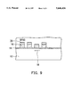
- FIG. 1 shows a plan view of a prior art mask ROM.
- FIG. 2 shows a cross-sectional view of the prior art mask ROM along the line II--II of FIG. 1.
- FIG. 3 shows a cross-sectional view of the prior art mask ROM along the line III--III of FIG. 1.
- the prior art mask ROM comprises: a P-type semiconductor substrate 10; a plurality of N+ type bit-lines 12 formed on the P-type semiconductor substrate 10 by the implantation of impurities there into; a gate oxide layer 14 formed on the surface of the P-type semiconductor substrate 10 and the bit-lines 12; and a plurality of word-lines 16 formed on the gate oxide layer 14, which together form an array of memory cells.
- the prior art technique for programming a memory cell of mask ROM 1 involves implanting an impurity 18 which prevents conduction between the two adjacent bit lines 12.
- This programming technique first involves forming a photoresist layer 20 over the substrate 10.
- conventional photolithography and etching techniques are used to form an opening 22.
- boron ions are implanted into the substrate 10 through the opening 22 to form a P type region 18 which is doped so heavily that conduction is cut off even when an electrical potential is applied to the overlying word-line 16.
- the foregoing prior art method has a drawback in that it is difficult to align the opening 22 accurately on the photoresist 20. If the opening is improperly positioned on the photoresist 20, that causes a side-diffusion effect which is problematic because it can affect the conduction state of adjacent memory cells. For example, a supposedly conducting memory cell can become non-conducing and vice versa due to this side-diffusion effect.
- a principal object of the present invention is to provide an effective and easily implemented method for coding the memory cells of a mask ROM.
- Another object of the present invention is to provide a self-aligned coding procedure for a mask ROM that resolves the aforementioned problem of ROM coding misalignment and the side-diffusion of doped impurities caused thereby.
- a method of self-aligned coding for a mask ROM is disclosed.
- a mask ROM with a silicon substrate, a plurality of bit-lines formed in the substrate, a gate oxide layer formed on the bit-lines, and a plurality of word-lines formed on the gate oxide, which together form an array of memory cells is provided.
- an aligning layer such as a silicon nitride or a silicon dioxide layer, is then formed over the word-lines.
- a photoresist is coated onto the surface of the aligning layer.
- openings are etched through portions of the photoresist not covered by a mask pattern.
- the etch occurs to the aligning layer.
- the resulting openings expose portions of the memory cells that are to be programmed as a first state, for example, an OFF state.
- the portion of the aligning layer beneath the openings is removed. Impurities are implanted into the substrate through the openings to enable or program selected memory cells to operate in a first state (OFF state) and to leave the remaining memory cells programmed to operate in a second state (ON state).
- the disclosed method provides a self-aligned implantation for mask ROM coding, wherein the aligning layer is positioned above the word-lines so that the openings in the photoresist layer act as a self-aligning mask. Accordingly, the problem of impurity side diffusion during coding is resolved without having to revise or add additional photo-masks.
- FIG. 1 is a plan view of a prior art mask ROM
- FIG. 2 is a cross-sectional view of the prior art mask ROM of FIG. 1 along the II--II line;
- FIG. 3 is a cross-sectional view of the prior art mask ROM of FIG. 1 along the III--III line;
- FIG. 4 to FIG. 9 schematically illustrate in cross-sectional representation one preferred embodiment according to the present invention.
- FIGS. 4 to 9 are cross-sectional illustrations of the mask ROM 1 during various stages of the coding process of this invention.
- the self-aligned implantation method of the present invention is suitable for coding the mask ROM 1 as shown in FIGS. 1 and 3.
- the disclosure hereinafter provided designates mask ROM parts embodying the method of the present invention with reference numerals similar to those of the prior art mask ROM to avoid repetition.
- the mask ROM 1 fabricated in accordance with the method of the present invention includes: a substrate 10 (N-type or P-type), a plurality of bit-lines 12 (not shown in FIGS. 4 to 9, but they are configured as is shown in FIGS. 1 and 2) formed in the substrate 10, a gate oxide 14 formed on the substrate 10, and a plurality word-lines 16 formed on the gate oxide 14 which together form the memory cells.
- the self-aligned mask ROM coding method of the present invention includes the following steps:
- FIG. 4 illustrates that the uncoded mask ROM 1 includes the gate oxide layer 14 which is formed with a gate oxide thickness of approximately 100 ⁇ 150 ⁇ (Angstrom).
- a polysilicon layer 16 (or a polycide layer such as WSi 2 ) with polysilicon layer thickness of approximately 3000 ⁇ is deposited over the gate oxide layer 14 by chemical vapor deposition (CVD).
- CVD chemical vapor deposition
- a silicon dioxide layer 30 or silicon nitride layer
- silicon dioxide layer 30 and the polysilicon layer 16 are patterned using conventional photolithography and etching techniques to form the word-lines 16 and an aligning layer 30.
- FIG. 5 shows that a photoresist layer 20a is then formed over the substrate 10.
- FIGS. 5 and 6 show that the photoresist layer 20a is patterned by a photo-mask 40 to form an opening 22a above a memory cell that is to be programmed to operate in a first conduction state. As is best illustrated in FIG. 6, the opening 22a is etched to the aligning layer 30 so that the layer 30 is exposed through the opening 22a.
- the disclosed invention utilizes this characteristic and properly controls the exposure conditions (intensity, timing . . . etc.) so that only an upper portion of the photoresist layer 20a above the word-lines 16 is developed to form the opening 22a as shown in FIG. 6.
- the exposure time is appropriately adjusted so that only the upper portion of the photoresist layer 20a is exposed.
- different types of photoresist require different exposure conditions.
- the method of the present invention is additionally advantageous in that it is not necessary to modify or add any photo-masks because the photo-mask 40 used in this step is similar to the one used in the prior art.
- the exposed portion of the aligning layer 30 within the opening 22a is removed. If the aligning layer 30 is made of silicon dioxide, it may be removed by applying buffered hydrofluoric acid (BHF). If the aligning layer 30 is made of silicon nitride, it may be removed by a dry etching procedure.
- BHF buffered hydrofluoric acid
- FIG. 8 shows that those memory cells which are to programmed to operate in a first state are programmed by implanting impurities to form a heavily doped region 18.
- impurities For example, boron ions may be implanted into the P-type substrate 10 with a dosage of 1 ⁇ 10 4 atoms/cm 2 and an implanting energy of 80 KeV to form the doped region 18, with the resulting programmed memory cell being isolated ("OFF") and the other undoped regions (i.e., a second state) being capable of ("ON").
- borophosphosilicate glass BPSG
- BPTEOS borophospho-tetraethylorthosilicate
- the disclosed invention provides a method of self-aligned mask ROM coding which is realized by positioning an aligning layer over the word-lines, thereby enabling the openings of the photoresist layer to self-align with the word-lines.
- the effect of "side diffusion" during the impurity implantation process for mask ROM coding is eliminated without requiring modifications to existing photo-masks or the use of additional masks.
- the shape of the resulting opening 22a as shown in FIG. 7, facilitates accurate ion implantation because the opening 22a narrows to vertically align itself with the edges of the word lines 16.
Abstract
A Read-Only Memory (ROM) device produced by self-aligned implantation. First, a non-coded mask ROM with a silicon substrate, a plurality of bit-lines formed in the substrate, a gate oxide layer formed on the bit-lines, and a plurality of word-lines formed on the gate oxide, which together form arrays of memory cells, is provided. Next, an aligning layer is formed above the word-lines. A photoresist is thereafter coated on the surface of the aligning layer. Then, portions of the photoresist not covered by a mask pattern are etched away to the aligning layer so as to provide openings exposing portions of the memory cells that will be programmed to operate in a first conduction state. Portions of the aligning layer exposed through the openings are then removed, after which impurities are implanted through the openings and into the substrate to enable the memory cells that are to operate in the first conduction state, and leave other non-programmed memory cells operating in a second conduction state.
Description
This is a divisional of application Ser. No. 08/264,461 filed Jun. 23, 1994, now abandoned.
1. Field of the Invention
The present invention relates generally to a mask ROM process with a self-aligned implantation, and more particularly, to a method of using photoresist as self-aligned mask for ROM coding to resolve the problem of side-diffusion which occurs during the subsequent impurity implantation process. The present invention also relates to the ROM produced by this process.
2. Description of the Prior Art
FIG. 1 shows a plan view of a prior art mask ROM. FIG. 2 shows a cross-sectional view of the prior art mask ROM along the line II--II of FIG. 1. FIG. 3 shows a cross-sectional view of the prior art mask ROM along the line III--III of FIG. 1. As is best illustrated in FIG. 2, the prior art mask ROM comprises: a P-type semiconductor substrate 10; a plurality of N+ type bit-lines 12 formed on the P-type semiconductor substrate 10 by the implantation of impurities there into; a gate oxide layer 14 formed on the surface of the P-type semiconductor substrate 10 and the bit-lines 12; and a plurality of word-lines 16 formed on the gate oxide layer 14, which together form an array of memory cells.
The prior art technique for programming a memory cell of mask ROM 1 involves implanting an impurity 18 which prevents conduction between the two adjacent bit lines 12. This programming technique first involves forming a photoresist layer 20 over the substrate 10. Next, conventional photolithography and etching techniques are used to form an opening 22. Thereafter, boron ions are implanted into the substrate 10 through the opening 22 to form a P type region 18 which is doped so heavily that conduction is cut off even when an electrical potential is applied to the overlying word-line 16.
However, the foregoing prior art method has a drawback in that it is difficult to align the opening 22 accurately on the photoresist 20. If the opening is improperly positioned on the photoresist 20, that causes a side-diffusion effect which is problematic because it can affect the conduction state of adjacent memory cells. For example, a supposedly conducting memory cell can become non-conducing and vice versa due to this side-diffusion effect.
A principal object of the present invention is to provide an effective and easily implemented method for coding the memory cells of a mask ROM.
Another object of the present invention is to provide a self-aligned coding procedure for a mask ROM that resolves the aforementioned problem of ROM coding misalignment and the side-diffusion of doped impurities caused thereby.
In accordance with the objects of the present invention, a method of self-aligned coding for a mask ROM is disclosed. First, a mask ROM with a silicon substrate, a plurality of bit-lines formed in the substrate, a gate oxide layer formed on the bit-lines, and a plurality of word-lines formed on the gate oxide, which together form an array of memory cells is provided. Pursuant to the disclosed method, an aligning layer, such as a silicon nitride or a silicon dioxide layer, is then formed over the word-lines. Thereafter, a photoresist is coated onto the surface of the aligning layer. Next, when the mask ROM is to be programmed, openings are etched through portions of the photoresist not covered by a mask pattern. The etch occurs to the aligning layer. The resulting openings expose portions of the memory cells that are to be programmed as a first state, for example, an OFF state. The portion of the aligning layer beneath the openings is removed. Impurities are implanted into the substrate through the openings to enable or program selected memory cells to operate in a first state (OFF state) and to leave the remaining memory cells programmed to operate in a second state (ON state).
The disclosed method provides a self-aligned implantation for mask ROM coding, wherein the aligning layer is positioned above the word-lines so that the openings in the photoresist layer act as a self-aligning mask. Accordingly, the problem of impurity side diffusion during coding is resolved without having to revise or add additional photo-masks.
The present invention can be more fully understood by referring to the following description and accompanying drawings, which form the integral part of this application:
FIG. 1 is a plan view of a prior art mask ROM;
FIG. 2 is a cross-sectional view of the prior art mask ROM of FIG. 1 along the II--II line;
FIG. 3 is a cross-sectional view of the prior art mask ROM of FIG. 1 along the III--III line;
FIG. 4 to FIG. 9 schematically illustrate in cross-sectional representation one preferred embodiment according to the present invention.
FIGS. 4 to 9 are cross-sectional illustrations of the mask ROM 1 during various stages of the coding process of this invention. The self-aligned implantation method of the present invention is suitable for coding the mask ROM 1 as shown in FIGS. 1 and 3. The disclosure hereinafter provided designates mask ROM parts embodying the method of the present invention with reference numerals similar to those of the prior art mask ROM to avoid repetition. The mask ROM 1 fabricated in accordance with the method of the present invention includes: a substrate 10 (N-type or P-type), a plurality of bit-lines 12 (not shown in FIGS. 4 to 9, but they are configured as is shown in FIGS. 1 and 2) formed in the substrate 10, a gate oxide 14 formed on the substrate 10, and a plurality word-lines 16 formed on the gate oxide 14 which together form the memory cells. The self-aligned mask ROM coding method of the present invention includes the following steps:
Step 1:
FIG. 4 illustrates that the uncoded mask ROM 1 includes the gate oxide layer 14 which is formed with a gate oxide thickness of approximately 100˜150 Å (Angstrom). Next, a polysilicon layer 16 (or a polycide layer such as WSi2) with polysilicon layer thickness of approximately 3000 Å is deposited over the gate oxide layer 14 by chemical vapor deposition (CVD). Then, a silicon dioxide layer 30 (or silicon nitride layer) with a silicon dioxide layer thickness of approximately 2000-3000 Å is deposited on the polysilicon layer 16. Thereafter, the silicon dioxide layer 30 and the polysilicon layer 16 are patterned using conventional photolithography and etching techniques to form the word-lines 16 and an aligning layer 30.
Step 2:
FIG. 5 shows that a photoresist layer 20a is then formed over the substrate 10.
Step 3;
FIGS. 5 and 6 show that the photoresist layer 20a is patterned by a photo-mask 40 to form an opening 22a above a memory cell that is to be programmed to operate in a first conduction state. As is best illustrated in FIG. 6, the opening 22a is etched to the aligning layer 30 so that the layer 30 is exposed through the opening 22a.
Although a limited depth of focus is an inherent problem for the photolithography process, the disclosed invention utilizes this characteristic and properly controls the exposure conditions (intensity, timing . . . etc.) so that only an upper portion of the photoresist layer 20a above the word-lines 16 is developed to form the opening 22a as shown in FIG. 6. The exposure time is appropriately adjusted so that only the upper portion of the photoresist layer 20a is exposed. As may be readily appreciated, different types of photoresist require different exposure conditions. The method of the present invention is additionally advantageous in that it is not necessary to modify or add any photo-masks because the photo-mask 40 used in this step is similar to the one used in the prior art.
Step 4:
In FIG. 7, the exposed portion of the aligning layer 30 within the opening 22a is removed. If the aligning layer 30 is made of silicon dioxide, it may be removed by applying buffered hydrofluoric acid (BHF). If the aligning layer 30 is made of silicon nitride, it may be removed by a dry etching procedure.
Step 5:
FIG. 8 shows that those memory cells which are to programmed to operate in a first state are programmed by implanting impurities to form a heavily doped region 18. For example, boron ions may be implanted into the P-type substrate 10 with a dosage of 1×10⁴ atoms/cm2 and an implanting energy of 80 KeV to form the doped region 18, with the resulting programmed memory cell being isolated ("OFF") and the other undoped regions (i.e., a second state) being capable of ("ON").
Step 6:
As is shown in FIG. 9, borophosphosilicate glass (BPSG) or borophospho-tetraethylorthosilicate (BPTEOS) with a thickness of approximately 5000-9000 Å is deposited over the implanted region, and then a metallization procedure is performed. The above-described procedures of this step are conventional and, therefore, are not further discussed.
In summary, the disclosed invention provides a method of self-aligned mask ROM coding which is realized by positioning an aligning layer over the word-lines, thereby enabling the openings of the photoresist layer to self-align with the word-lines. As a result, the effect of "side diffusion" during the impurity implantation process for mask ROM coding is eliminated without requiring modifications to existing photo-masks or the use of additional masks. The shape of the resulting opening 22a, as shown in FIG. 7, facilitates accurate ion implantation because the opening 22a narrows to vertically align itself with the edges of the word lines 16.
Although preferred embodiments for this invention are describe above, the disclosed invention is not limited to such embodiments. On the contrary, for anyone skilled in the arts, it is intended to cover various modifications and similar arrangements included within the spirit and scope of the appended claims, the scope of which should be accorded the broadest interpretation so as to encompass all such modifications and similar structures.
Claims (3)
1. A read only memory device comprising:
(a) a substrate with a plurality of conductive bit-lines formed therein, a gate oxide layer formed on said bit-lines, and a plurality of conductive word-lines formed on said gate oxide, which together form an array of memory cells; and
(b) selected ones of said memory cells being programmed to a first state by impurities implanted in said substrate and said selected cells, the remaining cells, which are not programmed to said first state, being characterized by an aligning layer of material which overlies said word-lines of said remaining cells, said material having sidewalls which align with sidewalls of said word-lines, and the selected ones of said memory cells being characterized by not having the aligning layer of material which overlies said word-lines of the selected ones, wherein said material is a layer of silicon dioxide.
2. A read only memory device comprising:
(a) a substrate with a plurality of conductive bit-lines formed therein, a gate oxide layer formed on said bit-lines, and a plurality of conductive word-lines formed on said gate oxide, which together form an array of memory cells;
(b) selected ones of said memory cells being programmed to a first state by impurities implanted in said substrate and said selected cells, the remaining cells, which are not programmed to said first state, being characterized by an aligning layer of material which overlies said word-lines of said remaining cells, said material having sidewalls which align with sidewalls of said word-lines, and the selected ones of said memory cells being characterized by not having the aligning layer of material which overlies said word-lines of the selected ones, wherein said material is a layer of silicon nitride.
3. A read only memory device comprising:
(a) a substrate with a plurality of conductive bit-lines formed therein, a gate oxide layer formed on said bit-lines, and a plurality of conductive word-lines formed on said gate oxide, which together form an array of memory cells;
(b) selected ones of said memory cells being programmed to a first state by impurities implanted in said substrate and said selected cells, the remaining cells, which are not programmed to said first state, being characterized by an aligning layer of material which overlies said word-lines of said remaining cells, said material having sidewalls which align with sidewalls of said word-lines, and the selected ones of said memory cells being characterized by not having the aligning layer of material which overlies said word-lines of the selected ones, wherein a BPSG layer is disposed over said word-lines and said material, said BPSG layer being in direct contact with upper surfaces of said word-lines for those cells programmed to said first conduction state and being spaced from said upper surfaces of said word-lines for those cells not programmed to said first conduction state.
Priority Applications (1)
| Application Number | Priority Date | Filing Date | Title |
|---|---|---|---|
| US08/536,934 US5646436A (en) | 1994-06-23 | 1995-09-29 | Read only memory (ROM) device produced by self-aligned implantation |
Applications Claiming Priority (2)
| Application Number | Priority Date | Filing Date | Title |
|---|---|---|---|
| US26446194A | 1994-06-23 | 1994-06-23 | |
| US08/536,934 US5646436A (en) | 1994-06-23 | 1995-09-29 | Read only memory (ROM) device produced by self-aligned implantation |
Related Parent Applications (1)
| Application Number | Title | Priority Date | Filing Date |
|---|---|---|---|
| US26446194A Division | 1994-06-23 | 1994-06-23 |
Publications (1)
| Publication Number | Publication Date |
|---|---|
| US5646436A true US5646436A (en) | 1997-07-08 |
Family
ID=23006171
Family Applications (2)
| Application Number | Title | Priority Date | Filing Date |
|---|---|---|---|
| US08/342,630 Expired - Lifetime US5576235A (en) | 1994-06-23 | 1994-11-21 | ROM coding process with self-aligned implantation and the ROM produced thereby |
| US08/536,934 Expired - Lifetime US5646436A (en) | 1994-06-23 | 1995-09-29 | Read only memory (ROM) device produced by self-aligned implantation |
Family Applications Before (1)
| Application Number | Title | Priority Date | Filing Date |
|---|---|---|---|
| US08/342,630 Expired - Lifetime US5576235A (en) | 1994-06-23 | 1994-11-21 | ROM coding process with self-aligned implantation and the ROM produced thereby |
Country Status (1)
| Country | Link |
|---|---|
| US (2) | US5576235A (en) |
Cited By (1)
| Publication number | Priority date | Publication date | Assignee | Title |
|---|---|---|---|---|
| US20040167502A1 (en) * | 2003-02-25 | 2004-08-26 | Weckwerth Mark V. | Optical sensor and method for identifying the presence of skin |
Families Citing this family (1)
| Publication number | Priority date | Publication date | Assignee | Title |
|---|---|---|---|---|
| US5589414A (en) * | 1995-06-23 | 1996-12-31 | Taiwan Semiconductor Manufacturing Company Ltd. | Method of making mask ROM with two layer gate electrode |
Citations (2)
| Publication number | Priority date | Publication date | Assignee | Title |
|---|---|---|---|---|
| US5394356A (en) * | 1993-03-22 | 1995-02-28 | United Microelectronics Corporation | Process for forming an FET read only memory device |
| US5472898A (en) * | 1994-08-09 | 1995-12-05 | United Microelectronics Corp. | Process for making a mask ROM with self-aligned coding technology |
Family Cites Families (3)
| Publication number | Priority date | Publication date | Assignee | Title |
|---|---|---|---|---|
| US4513494A (en) * | 1983-07-19 | 1985-04-30 | American Microsystems, Incorporated | Late mask process for programming read only memories |
| US5149667A (en) * | 1989-05-31 | 1992-09-22 | Samsung Electronics Co., Ltd. | Mask ROM device having double polycrystalline silicone and process for producing the same |
| US5200355A (en) * | 1990-12-10 | 1993-04-06 | Samsung Electronics Co., Ltd. | Method for manufacturing a mask read only memory device |
-
1994
- 1994-11-21 US US08/342,630 patent/US5576235A/en not_active Expired - Lifetime
-
1995
- 1995-09-29 US US08/536,934 patent/US5646436A/en not_active Expired - Lifetime
Patent Citations (2)
| Publication number | Priority date | Publication date | Assignee | Title |
|---|---|---|---|---|
| US5394356A (en) * | 1993-03-22 | 1995-02-28 | United Microelectronics Corporation | Process for forming an FET read only memory device |
| US5472898A (en) * | 1994-08-09 | 1995-12-05 | United Microelectronics Corp. | Process for making a mask ROM with self-aligned coding technology |
Cited By (1)
| Publication number | Priority date | Publication date | Assignee | Title |
|---|---|---|---|---|
| US20040167502A1 (en) * | 2003-02-25 | 2004-08-26 | Weckwerth Mark V. | Optical sensor and method for identifying the presence of skin |
Also Published As
| Publication number | Publication date |
|---|---|
| US5576235A (en) | 1996-11-19 |
Similar Documents
| Publication | Publication Date | Title |
|---|---|---|
| US6706594B2 (en) | Optimized flash memory cell | |
| US5902121A (en) | Semiconductor device and method for manufacturing semiconductor device | |
| US6211014B1 (en) | Three-dimensional, deep-trench, high-density read-only memory (ROM) and its manufacturing method | |
| EP0412558A2 (en) | Method of manufacturing nonvolatile semiconductor memories | |
| KR19990048973A (en) | Semiconductor device and manufacturing method thereof | |
| US5384478A (en) | Mask ROM process | |
| US6294422B1 (en) | Semiconductor device with high integration density and improved performance | |
| US6790721B2 (en) | Metal local interconnect self-aligned source flash cell | |
| KR100223832B1 (en) | Method of manufacturing semiconductor device | |
| US5652152A (en) | Process having high tolerance to buried contact mask misalignment by using a PSG spacer | |
| US5472898A (en) | Process for making a mask ROM with self-aligned coding technology | |
| US5631481A (en) | Flat-cell mask ROM integrated circuit | |
| US5661326A (en) | Mask ROM process with self-aligned ROM code implant | |
| US5529942A (en) | Self-aligned coding process for mask ROM | |
| US5550075A (en) | Ion implanted programmable cell for read only memory applications | |
| US6573574B2 (en) | Cell array region of a NOR-type mask ROM device and fabricating method therefor | |
| KR100251229B1 (en) | Advanced nor type read only memory and fabricating method thereof | |
| US5646436A (en) | Read only memory (ROM) device produced by self-aligned implantation | |
| US5572056A (en) | High density ROM | |
| US5208173A (en) | Method of manufacturing non-volatile semiconductor memory device | |
| US5648289A (en) | Method for coding semiconductor read only memory device | |
| US6218247B1 (en) | Method for fabricating mask ROM | |
| US20030011018A1 (en) | Flash floating gate using epitaxial overgrowth | |
| US6537882B1 (en) | Method of fabricating a semiconductor device in which no side walls are formed adjacent the gates of the MOSFETs of the memory cell | |
| KR0123745B1 (en) | Contact formation method of semiconductor device |
Legal Events
| Date | Code | Title | Description |
|---|---|---|---|
| STCF | Information on status: patent grant |
Free format text: PATENTED CASE |
|
| FPAY | Fee payment |
Year of fee payment: 4 |
|
| FEPP | Fee payment procedure |
Free format text: PAYOR NUMBER ASSIGNED (ORIGINAL EVENT CODE: ASPN); ENTITY STATUS OF PATENT OWNER: LARGE ENTITY |
|
| FPAY | Fee payment |
Year of fee payment: 8 |
|
| FPAY | Fee payment |
Year of fee payment: 12 |