US5628031A - Personal digital assistant module implemented as a low-profile printed circuit assembly having a rigid substrate wherein IC devices are mounted within openings wholly between opposite plane surfaces of the rigid substrate - Google Patents
Personal digital assistant module implemented as a low-profile printed circuit assembly having a rigid substrate wherein IC devices are mounted within openings wholly between opposite plane surfaces of the rigid substrate Download PDFInfo
- Publication number
- US5628031A US5628031A US08/335,325 US33532594A US5628031A US 5628031 A US5628031 A US 5628031A US 33532594 A US33532594 A US 33532594A US 5628031 A US5628031 A US 5628031A
- Authority
- US
- United States
- Prior art keywords
- digital assistant
- μpda
- assistant module
- host
- enclosure
- Prior art date
- Legal status (The legal status is an assumption and is not a legal conclusion. Google has not performed a legal analysis and makes no representation as to the accuracy of the status listed.)
- Expired - Fee Related
Links
Images


Classifications
-
- H—ELECTRICITY
- H04—ELECTRIC COMMUNICATION TECHNIQUE
- H04M—TELEPHONIC COMMUNICATION
- H04M1/00—Substation equipment, e.g. for use by subscribers
- H04M1/26—Devices for calling a subscriber
- H04M1/27—Devices whereby a plurality of signals may be stored simultaneously
- H04M1/274—Devices whereby a plurality of signals may be stored simultaneously with provision for storing more than one subscriber number at a time, e.g. using toothed disc
- H04M1/2745—Devices whereby a plurality of signals may be stored simultaneously with provision for storing more than one subscriber number at a time, e.g. using toothed disc using static electronic memories, e.g. chips
- H04M1/275—Devices whereby a plurality of signals may be stored simultaneously with provision for storing more than one subscriber number at a time, e.g. using toothed disc using static electronic memories, e.g. chips implemented by means of portable electronic directories
-
- G—PHYSICS
- G06—COMPUTING; CALCULATING OR COUNTING
- G06F—ELECTRIC DIGITAL DATA PROCESSING
- G06F1/00—Details not covered by groups G06F3/00 - G06F13/00 and G06F21/00
- G06F1/16—Constructional details or arrangements
- G06F1/1613—Constructional details or arrangements for portable computers
- G06F1/1626—Constructional details or arrangements for portable computers with a single-body enclosure integrating a flat display, e.g. Personal Digital Assistants [PDAs]
-
- G—PHYSICS
- G06—COMPUTING; CALCULATING OR COUNTING
- G06F—ELECTRIC DIGITAL DATA PROCESSING
- G06F1/00—Details not covered by groups G06F3/00 - G06F13/00 and G06F21/00
- G06F1/16—Constructional details or arrangements
- G06F1/1613—Constructional details or arrangements for portable computers
- G06F1/1632—External expansion units, e.g. docking stations
-
- G—PHYSICS
- G06—COMPUTING; CALCULATING OR COUNTING
- G06F—ELECTRIC DIGITAL DATA PROCESSING
- G06F1/00—Details not covered by groups G06F3/00 - G06F13/00 and G06F21/00
- G06F1/16—Constructional details or arrangements
- G06F1/1613—Constructional details or arrangements for portable computers
- G06F1/1633—Constructional details or arrangements of portable computers not specific to the type of enclosures covered by groups G06F1/1615 - G06F1/1626
- G06F1/1656—Details related to functional adaptations of the enclosure, e.g. to provide protection against EMI, shock, water, or to host detachable peripherals like a mouse or removable expansions units like PCMCIA cards, or to provide access to internal components for maintenance or to removable storage supports like CDs or DVDs, or to mechanically mount accessories
-
- G—PHYSICS
- G06—COMPUTING; CALCULATING OR COUNTING
- G06F—ELECTRIC DIGITAL DATA PROCESSING
- G06F1/00—Details not covered by groups G06F3/00 - G06F13/00 and G06F21/00
- G06F1/16—Constructional details or arrangements
- G06F1/18—Packaging or power distribution
- G06F1/183—Internal mounting support structures, e.g. for printed circuit boards, internal connecting means
-
- G—PHYSICS
- G06—COMPUTING; CALCULATING OR COUNTING
- G06F—ELECTRIC DIGITAL DATA PROCESSING
- G06F1/00—Details not covered by groups G06F3/00 - G06F13/00 and G06F21/00
- G06F1/16—Constructional details or arrangements
- G06F1/20—Cooling means
- G06F1/203—Cooling means for portable computers, e.g. for laptops
-
- G—PHYSICS
- G06—COMPUTING; CALCULATING OR COUNTING
- G06F—ELECTRIC DIGITAL DATA PROCESSING
- G06F1/00—Details not covered by groups G06F3/00 - G06F13/00 and G06F21/00
- G06F1/16—Constructional details or arrangements
- G06F1/20—Cooling means
- G06F1/206—Cooling means comprising thermal management
-
- G—PHYSICS
- G06—COMPUTING; CALCULATING OR COUNTING
- G06F—ELECTRIC DIGITAL DATA PROCESSING
- G06F13/00—Interconnection of, or transfer of information or other signals between, memories, input/output devices or central processing units
- G06F13/38—Information transfer, e.g. on bus
- G06F13/40—Bus structure
- G06F13/4063—Device-to-bus coupling
- G06F13/409—Mechanical coupling
-
- G—PHYSICS
- G06—COMPUTING; CALCULATING OR COUNTING
- G06F—ELECTRIC DIGITAL DATA PROCESSING
- G06F21/00—Security arrangements for protecting computers, components thereof, programs or data against unauthorised activity
- G06F21/60—Protecting data
- G06F21/62—Protecting access to data via a platform, e.g. using keys or access control rules
-
- G—PHYSICS
- G06—COMPUTING; CALCULATING OR COUNTING
- G06F—ELECTRIC DIGITAL DATA PROCESSING
- G06F3/00—Input arrangements for transferring data to be processed into a form capable of being handled by the computer; Output arrangements for transferring data from processing unit to output unit, e.g. interface arrangements
- G06F3/01—Input arrangements or combined input and output arrangements for interaction between user and computer
- G06F3/048—Interaction techniques based on graphical user interfaces [GUI]
- G06F3/0481—Interaction techniques based on graphical user interfaces [GUI] based on specific properties of the displayed interaction object or a metaphor-based environment, e.g. interaction with desktop elements like windows or icons, or assisted by a cursor's changing behaviour or appearance
- G06F3/0482—Interaction with lists of selectable items, e.g. menus
-
- H—ELECTRICITY
- H04—ELECTRIC COMMUNICATION TECHNIQUE
- H04M—TELEPHONIC COMMUNICATION
- H04M1/00—Substation equipment, e.g. for use by subscribers
- H04M1/72—Mobile telephones; Cordless telephones, i.e. devices for establishing wireless links to base stations without route selection
- H04M1/725—Cordless telephones
-
- H—ELECTRICITY
- H04—ELECTRIC COMMUNICATION TECHNIQUE
- H04M—TELEPHONIC COMMUNICATION
- H04M11/00—Telephonic communication systems specially adapted for combination with other electrical systems
- H04M11/06—Simultaneous speech and data transmission, e.g. telegraphic transmission over the same conductors
-
- H—ELECTRICITY
- H04—ELECTRIC COMMUNICATION TECHNIQUE
- H04M—TELEPHONIC COMMUNICATION
- H04M3/00—Automatic or semi-automatic exchanges
- H04M3/42—Systems providing special services or facilities to subscribers
- H04M3/42314—Systems providing special services or facilities to subscribers in private branch exchanges
-
- H—ELECTRICITY
- H05—ELECTRIC TECHNIQUES NOT OTHERWISE PROVIDED FOR
- H05K—PRINTED CIRCUITS; CASINGS OR CONSTRUCTIONAL DETAILS OF ELECTRIC APPARATUS; MANUFACTURE OF ASSEMBLAGES OF ELECTRICAL COMPONENTS
- H05K5/00—Casings, cabinets or drawers for electric apparatus
- H05K5/02—Details
- H05K5/0256—Details of interchangeable modules or receptacles therefor, e.g. cartridge mechanisms
- H05K5/026—Details of interchangeable modules or receptacles therefor, e.g. cartridge mechanisms having standardized interfaces
- H05K5/0265—Details of interchangeable modules or receptacles therefor, e.g. cartridge mechanisms having standardized interfaces of PCMCIA type
- H05K5/0273—Details of interchangeable modules or receptacles therefor, e.g. cartridge mechanisms having standardized interfaces of PCMCIA type having extensions for peripherals, e.g. LAN, antennas
-
- H—ELECTRICITY
- H04—ELECTRIC COMMUNICATION TECHNIQUE
- H04M—TELEPHONIC COMMUNICATION
- H04M1/00—Substation equipment, e.g. for use by subscribers
- H04M1/247—Telephone sets including user guidance or feature selection means facilitating their use
- H04M1/2473—Telephone terminals interfacing a personal computer, e.g. using an API (Application Programming Interface)
-
- H—ELECTRICITY
- H04—ELECTRIC COMMUNICATION TECHNIQUE
- H04M—TELEPHONIC COMMUNICATION
- H04M3/00—Automatic or semi-automatic exchanges
- H04M3/42—Systems providing special services or facilities to subscribers
- H04M3/42314—Systems providing special services or facilities to subscribers in private branch exchanges
- H04M3/42323—PBX's with CTI arrangements
Definitions
- This invention is in the area of portable computers and pertains more specifically to small portable computing devices known in the art as personal digital assistants, and to manufacturing techniques for producing such devices.
- PDA Personal Digital Assistant
- a big drawback of the PDA systems being offered is the way they transfer data between a user's desktop unit, or other host, and the PDA.
- Known communication is by modem, by infrared communication, and by serial connection. These all require manipulation by a user, modulation on one or both ends of the communication path, and the like, which can be time-consuming, error-prone, and hardware extensive (expensive).
- Presently the Newton offers a modem and/or LED communication as an option, adding to the overall cost.
- a very important feature of the ⁇ PDA in an aspect of the present invention is a direct parallel bus interface with a connector allowing the unit to be docked by plugging it into a docking bay in a host unit. Moreover, when the ⁇ PDA is docked in the host, there needs to be a means to effectively disable the CPU in the ⁇ PDA and to provide direct access to both the ⁇ PDA software and data storage by the host CPU. This direct access would provide immediate ability to communicate in the fastest available fashion between the ⁇ PDA and the host, and would also facilitate additional important features to be described below.
- the ⁇ PDA also needs to have an optional compressed bus interface, including a connector separate from the host interface, so add-on devices may be utilized, such as a FAX modem, cellular communication, printer, and so on.
- add-on devices such as a FAX modem, cellular communication, printer, and so on.
- An additional feature that could be optionally provided in another aspect of the invention is an interface at the host to allow a user to select pre-arranged software mixes for loading to the ⁇ PDA.
- This feature comprises a set of control routines operating in conjunction with the host's display and input means, to allow the user to quickly select applications and perhaps data as well to be loaded to the ⁇ PDA satellite, to configure the smaller, more portable unit for specific itineraries and purposes.
- Another desirable feature is an ability to automatically update data files.
- data on the host if carrying a later date and/or time stamp than the data on the ⁇ PDA, would be automatically updated on the ⁇ PDA and vice-versa.
- the host gains access, determines the location of the latest files, and accomplishes the update.
- This feature needs to have some built-in user prompting to be most effective. It makes the ⁇ PDA a true satellite system.
- a personal digital assistant module comprising an enclosure for enclosing and supporting internal elements, a microcontroller within the enclosure for performing digital operations to manage functions of the personal digital assistant module, and a memory connected to the microcontroller by a bus structure for storing data and executable routines.
- a power supply within the enclosure for supplying power to functional elements of the personal digital assistant module, and a touchscreen combination display/input apparatus implemented on a surface of the enclosure.
- a host interface means comprising a host interface bus structure, which may be configured as a PCMCIA bus interface, is connected to the microcontroller and to a first portion of a host interface connector at a surface of the enclosure, and the host interface means is configured to directly connect the microcontroller to a compatible bus structure of a host computer.
- the elements of the personal digital assistant module are assembled with IC elements, such as the microcontroller and the memory device, enclosed within openings in a rigid substrate, with bus traces and other interconnects inplemented on a surface of the substrate.
- the personal digital assistant module has an expansion bus interface comprising an expansion bus structure connected to the microcontroller and to a first portion of an expansion bus connector for connecting the microcontroller to a peripheral device.
- an expansion bus interface comprising an expansion bus structure connected to the microcontroller and to a first portion of an expansion bus connector for connecting the microcontroller to a peripheral device.
- the personal digital assistant module also has a nonvolatile storage device, such as an EEPROM connected to the microcontroller and containing one or more codes unique to the personal digital assistant, for uniquely identifying the personal digital assistant to digital devices connected on the host interface.
- a nonvolatile storage device such as an EEPROM connected to the microcontroller and containing one or more codes unique to the personal digital assistant, for uniquely identifying the personal digital assistant to digital devices connected on the host interface.
- the display and input means for the personal digital assistant are configured as an overlaid touch screen and LCD display on a surface of the outer case of the personal digital assistant.
- a pointer device implemented as a thumbwheel in one embodiment and as a pressure sensitive pad in another is provided as part of the input capability.
- the personal digital assistant module forms a unique combination with a general-purpose computer host having the personal digital assistant as a satellite unit.
- the host in this instance has a docking bay especially configured to dock the personal digital assistant, making a direct bus connection between the local CPU of the personal digital assistant and the CPU of the host.
- the host may be a desktop unit, a notebook computer, or a smaller portable like a palmtop computer. This combination provides power and convenience not before available.
- Many other digital devices are also provided according to various aspects of the invention, such as modems, scanners, data acquisition peripherals, cellular phones, and a software vending machine, and all of these devices may be appended to the personal digital assistant by the expansion bus interface or, in many cases, by the host interface.
- the personal digital assistant provided according to embodiments of the present invention is a unit more compact than conventional PDAs. It represents a new dimension in computer application and applicability, in a form promising to be eminently usable by and useful to almost everyone; and at a price easily affordable. It solves the communication problem intrinsic to personal digital assistants relative to larger and more powerful computers, with a unit that fits into a user's breast pocket, and at a very low price.
- FIG. 1A is an isometric view of a ⁇ PDA according to an embodiment of the present invention.
- FIG. 1B is a plan view of the ⁇ PDA of FIG. 1A.
- FIG. 2 is a cross-sectional view of the ⁇ PDA of FIGS. 1A and 1B.
- FIG. 3 is a block diagram of the ⁇ PDA of FIG. 1A and some peripheral elements.
- FIG. 4 is a more detailed plan view of the ⁇ PDA of FIG. 1A showing in particular an LCD display and touch screen user interface in an aspect of the present invention.
- FIG. 5 is an isometric view of a ⁇ PDA and a host notebook computer in an aspect of the present invention, with the ⁇ PDA about to be docked in a docking bay of the notebook computer.
- FIG. 6 is a block diagram of a ⁇ PDA docked in a docking bay of a host computer according to an embodiment of the present invention.
- FIG. 7 is a logic flow diagram of the steps in docking a ⁇ PDA in a host computer according to an embodiment of the present invention.
- FIG. 8 is an isometric illustration of a ⁇ PDA software vending machine in an aspect of the present invention.
- FIG. 9 is a top plan view of a ⁇ PDA enhanced user interface according to an embodiment of the present invention.
- FIG. 10 is a top plan view of a ⁇ PDA with a microphone in an embodiment of the present invention.
- FIG. 11 is an isometric drawing of a ⁇ PDA docked in a dedicated cellular or cordless telephone according to an embodiment of the present invention.
- FIG. 12 is a plan view of a ⁇ PDA with a speaker and pager interface according to an embodiment of the present invention.
- FIG. 13 is a plan view of a ⁇ PDA with an infrared communication interface according to an embodiment of the present invention.
- FIG. 14 is a plan view of a ⁇ PDA with a scanner attachment according to an embodiment of the present invention.
- FIG. 15 is a plan view of a ⁇ PDA with a fax-modem attached according to an embodiment of the present invention.
- FIG. 16 is a plan view of a ⁇ PDA with a printer adapter interface according to an embodiment of the present invention.
- FIG. 17 is an isometric drawing of a ⁇ PDA docked in a barcode reader providing a data acquisition peripheral according to an embodiment of the present invention.
- FIG. 18 is an isometric view of a ⁇ PDA with a solar charger according to an embodiment of the present invention.
- FIG. 19 is a plan view of four ⁇ PDAs interfaced to a dedicated network console providing inter-PDA communication according to an embodiment of the present invention.
- FIG. 20 is an isometric view of a ⁇ PDA according to the invention connected by the expansion port to a standard-sized keyboard.
- FIG. 21A shows a motherboard and PCB modules in a conventional configuration.
- FIG. 21B shows a conventional connection technology.
- FIG. 21C is an illustration of a DRAM module as known in the art.
- FIG. 21D is a partial sectional view of a typical IC soldered to a board, showing a lead configuration.
- FIG. 22 is an idealized cross-sectional view of a conventional multilayer printed circuit board.
- FIG. 23A is an idealized cross-sectional view of a conventional single-sided DRAM memory module.
- FIG. 23B is an idealized cross-sectional view of a conventional double-sided DRAM memory module.
- FIG. 24 is a cross-sectional illustration of a multi-layered PCB according to an embodiment of the present invention.
- FIG. 25A is a plan view of one side of a memory module card according to an embodiment of the present invention, before adding DRAM ICs.
- FIG. 25B is a plan view of the opposite side of the memory module card of FIG. 25A.
- FIG. 25C is an elevation view of the memory module card of FIG. 25A.
- FIG. 25D is an elevation view of an assembled card with DRAMs according to the embodiment of the embodiment of FIGS. 25A, B, and C.
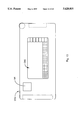
- FIG. 1A is an isometric view of a ⁇ PDA 10 according to an embodiment of the present invention.
- the unit is modeled on the PCMCIA standard Type II form factor, having a height D1 of about 5 mm.
- Body 12 is described in further detail below, and has a female portion 14 of a connector recessed at one end for engaging a mating male portion of the connector in a host computer, connecting the ⁇ PDA internal circuitry directly with a host internal bus.
- the host unit may be a notebook computer having a docking bay for the ⁇ PDA. Docking bays may be provided in desktop and other types of computers, and even in other kinds of digital equipment, several examples of which are described below.
- a combination I/O interface 16 implemented on one side of the ⁇ PDA, comprising a display overlaid with a touch-sensitive planar structure providing softkey operation in conjunction with interactive control routines operable on the ⁇ PDA in a stand-alone mode.
- FIG. 1A there may also be guides implemented along the sides of the case of the device for guiding the module in and out of a docking bay in a host computer unit. There may also be one or more mechanical features facilitating engagement and disengagement of the module in a docking bay.
- FIG. 1B is a top plan view of the ⁇ PDA of FIG. 1A, showing a thumbwheel 18 implemented in one corner of the ⁇ PDA.
- the thumbwheel in this embodiment is an input device capable of providing input with both amplitude and directional characteristics, and in some cases rate characteristics as well.
- the thumbwheel has many uses in combination with the ⁇ PDA and I/O interface 16. One such use is controlled scrolling of icons, characters, menus, and the like on the display of the device.
- the thumbwheel provides many of the functions of a pointer device.
- a second external connector portion 20 is provided. This connector portion is for engaging peripheral devices as part of an expansion bus interface.
- FIG. 2 is a simplified cross-sectional view of a means for constructing a ⁇ PDA according to the present invention in a Type II PCMCIA, or other relatively small package.
- ICs 34 are encapsulated in a conformal material 36, and interconnection is accomplished by traces on a flexible polymer film 32 shown as overlaying the encapsulated structure.
- the ICs are not packaged in the conventional manner having solder leads for assembly to a printed circuit board. Rather, connections are made directly between the solder pads on the chip and the traces on the Kapton film.
- ICs indicated by element No. 34 with specific functional ICs in a ⁇ PDA. This cross-section is illustrative of a method of construction only.
- LCD display 25 is implemented on one side of the ⁇ PDA, and touch-sensitive interface 27 is provided overlaying at least a portion of the LCD display.
- a metal casing 38 or other suitable material or combinations of material, surrounds the internal components and conforms to Type II PCMCIA form factors. This simplified cross-section illustrates some of the principles of construction that can allow the needed components to be inexpensively fitted into the small form factor needed.
- the ⁇ PDA is implemented in the form factor of a type III (10 mm thick) PCMCIA unit, using relatively conventional technology, such as PCB technology, rather than the encapsulated construction described immediately above.
- Various other constructions, form factors, and combinations are possible, as well.
- FIG. 3 is a simplified electrical block diagram of the ⁇ PDA of FIGS. 1A, 1B and 2.
- a unique microcontroller 11 acts as the CPU of the ⁇ PDA in the stand-alone mode, that is, when the ⁇ PDA is not docked in a host unit.
- microcontroller 11 acts as a slave unit, granting bus control to the CPU of the host.
- the CPU of the host In docked mode, the CPU of the host thus gains control of the memory contents of the ⁇ PDA, subject in most cases to security procedures which are described below.
- the host computer can transfer data and software into and out of a docked ⁇ PDA memory. In other embodiments many other cooperative operating modes may be accomplished between the two CPUs and accessible memory devices.
- Memory 13 is preferably a nonvolatile device from 1 to 2 megabytes in this embodiment, and both control routines for applications and data files are stored in this memory.
- Memory 13 may be flash memory, CMOS ROM, CMOS RAM with battery, or a combination, with the software stored in ROM and the data in the flash memory.
- the memory device is interfaced to microcontroller 11 via a dedicated bus structure 17, and microprocessor 11 is configured to drive memory bus 17.
- a battery 15 is the power source in the stand-alone mode, and may be recharged in one or more of several ways.
- the power traces are not shown in FIG. 3, but extend to all of the powered devices in the ⁇ PDA module.
- the host power source may be connected to pins through the host interface to recharge the battery.
- an attached means such as a solar panel may be configured to charge the battery and/or provide power to the ⁇ PDA.
- a solar panel for power is described elsewhere in this disclosure.
- the battery may be easily removed for periodic replacement.
- Host bus connector 14 is a part of a host interface which comprises a bus structure 26 for providing connection to the host in docked mode, as described above.
- the host interface is according to PCMCIA Type II, Rev. 3 standard, which is capable of communication either in PCMCIA mode or in a mode similar to PCI mode.
- PCI mode refers to a high-speed intermediate bus protocol being developed by Intel corporation, expected to become a standard bus architecture and protocol in the industry.
- the physical interface at the host in this embodiment is a slot-like docking bay, as is typical of know docking bays for PCMCIA devices. This docking bay may be implemented as a docking box, a built-in unit like a floppy-drive unit, or it may take some other form.
- Connector portion 20 is a part of the expansion bus interface described above, comprising a dedicated bus structure 40 connected to microcontroller 11.
- This interface can be implemented in a number of different ways.
- the purpose of the optional expansion bus interface is to connect to optional peripheral devices, such as a printer, a FAX modem, a host cellular phone, and others.
- the expansion bus interface is not an essential feature in a minimum embodiment of the present invention, but provides vastly enhanced functionality in many embodiments.
- the expansion interface can take any one of several forms.
- a preferred form is an extended enhanced parallel port and protocol based on an invention by the present inventors disclosed in a copending patent application.
- Another form is an indexed I/O port having 8-bit address and 8-bit data capability.
- the requirement of the expansion port is that the connection and communication protocol be compatible with expansion devices, such as telephone modems, fax modems, scanners, and the like. Many other configurations are possible.
- Optional equipment such as devices listed in box 19 may be connected for use with the ⁇ PDA through the expansion bus. Selected ones of such devices may also be built in to the ⁇ PDA in various embodiments, providing variations of applicability. In the former case, connection is through path 21 and the expansion bus interface via connector portion 20. In the built-in case, connection is in the interconnection traces of the ⁇ PDA as indicated by path 23.
- I/O interface 16 (also FIG. 1B) is for viewing ⁇ PDA application-related data and for touch-sensitive input via softkeys.
- softkeys is meant assignment by software of various functions to specific touch sensitive screen areas, which act as input keys.
- Labels in I/O interface 16 identify functionality of the touch-sensitive areas in various operating modes according to installed machine control routines. LCD display 25 and the touch-sensitive area 27 together form the combination I/O interface 16 described also above.
- data and program security comprising an Electrically Erasable Programmable Read Only Memory (EEPROM) 31, which is connected by dedicated communication lines to microcontroller 11.
- EEPROM 31 holds one or more codes installed at the point of manufacturing to provide security for information transfer between a host and a ⁇ PDA. The purpose is to control access by a host to the memory contents of a ⁇ PDA, so each ⁇ PDA may be configured to an individual. To accomplish this, docking and bus mastering machine control routines are initiated at the point of docking, and this security process is described in more detail below.
- security codes may be provided by a Read Only Memory (ROM) chip or other permanent or semi-permanent memory source.
- FIG. 4 is a plan view similar to FIG. 1B, of a ⁇ PDA, showing in particular I/O interface 16.
- I/O interface 16 may vary, but in general occupies a major portion of one of the sides of the module.
- I/O interface 16 comprises an LCD display with a resolution of 256 by 144 pixels in a screen size that displays 32 by 12 characters. Each character in this embodiment is displayed in an area eight pixels wide and twelve pixels high. In another embodiment, the pixel resolution is 320 by 200, which corresponds to 40 by 16 characters.
- the touch-sensitive areas of the touch-sensitive screen correspond to the character areas of the display. By touching an area with a finger or stylus, data can be entered quite quickly and with minimal CPU demand.
- thumbwheel 18 provides a two-directional means of controlling the configuration of the display according to installed control routines.
- a menu 70 is configured at one side to represent the current status of any application in progress and to provide appropriate user menu selections.
- input from thumbwheel 18 is used for scrolling through menu 70, and active areas may be indicated by a cursor.
- a user makes a menu selection by pressing the appropriate touch-sensitive area.
- a specific input may be provided to cause the menu area to be displayed on either side of the display according to a user's preference.
- thumbwheel 18 may be configured to allow for scrolling and panning.
- a document window 72 is provided in this embodiment at the top or bottom of I/O interface 16.
- a cursor locates the active position within the document for editing purposes.
- Menu 70 provides selection of available fonts, and input by thumbwheel 18 controls cursor movement over the document.
- rotating thumbwheel 18 in one direction may display horizontal strips of a document, while rotating the thumbwheel in the opposite direction moves the window vertically strips of the same document.
- a soft key or optional hard key may be configured to switch between the document and keyboard window, and the same or another key may be configured to switch between scrolling left or right, up or down, document or keyboard.
- a switch key may be used to change the thumbwheel mode of operation.
- a switch key may also be used in combination with a floating pointer to select characters and menu items. In this embodiment, the user can keep his or her hands relatively stationary on just the thumbwheel and the switch key, making all possible selections. Use of a a switch key in combination with a floating pointer facilitates the use of small fonts.
- a switch key may also be incorporated as an additional hard key in a convenient location on the case 12.
- a further embodiment of the present invention provides an I/O set-up application wherein a user may completely customize features of I/O area displays.
- the four-way force-sensitive mouse button can provide menu scrolling of a cursor and panning and/or indexing of keyboard and document windows, while the selector button is used to select and edit according to position of a cursor. This configuration minimizes hand movement and keeps the I/O area clear for viewing.
- thumbwheels including the translation of mechanical motion and pressure to electrical signals and provision of such signals to a microcontroller. For this reason, details of such interfaces are not provided in this disclosure. Combinations of such inputs with displays and input areas may, however, be considered as inventive.
- FIG. 5 is an isometric drawing of a ⁇ PDA 10 in position to be docked in a notebook computer 172 via a Type II PCMCIA docking port 105 according to an embodiment of the present invention.
- the ⁇ PDA is activated and a procedure is initiated with the host computer to manage communication and verify memory access rights (security).
- Access rights are considered important by the inventors for a number of reasons. Firstly, through the expedient of one or more specific codes, unique to each ⁇ PDA, a user may protect files stored in his module from access by unauthorized persons.
- the code can be used both to control access to data and files via I/O interface 16, and also through the host bus interface, so data and files may be secure from access by an unauthorized host system.
- an application routine can query the user for an access code to be entered at I/O interface 16 FIG. 4). If the code is not entered properly, access is denied, and power goes off.
- Codes for the purpose are stored in EEPROM 31 (FIG. 3), or in whatever ROM device may be devoted to the purpose. In some embodiments, the code may by mask-programmed at manufacture, so it is not alterable. In others, the code may be accessible and changeable by special procedures in the field.
- a portable or desktop computer may have a docking port physically configured to receive a ⁇ PDA, yet not be configured to communicate with the ⁇ PDA. This certainly might be the case where the ⁇ PDA is in the PCMCIA form.
- this specification terms such a unit a generic host. If the unit is configured to communicate with a ⁇ PDA it is an enabled host. If a host is configured for full access to a particular ⁇ PDA, it is a dedicated host.
- a docking unit is a generic host, there will be no communication unless the person presenting the ⁇ PDA provides the control routines to the host. This may be done for a generic host such as by transfer from a floppy disk, from a separate memory card through the docking port, or, in some embodiments, the communication software may be resident in memory 13 (FIG. 3) of a docked ⁇ PDA, transferrable to the host to facilitate further communication.
- the stored code or codes in EEPROM 31 may be used to verify authorization for data and program transfer between the host and a ⁇ PDA.
- this procedure is in the following order: First, when one docks a ⁇ PDA in a compatible docking port, certain pin connections convey to both the ⁇ PDA microcontroller and to the host CPU that the module is docked. Assuming an enabled host, the fact of docking commences an initialization protocol on both systems.
- the docking unit is a non-host, that is, it is not capable of communication with the docked module, nothing happens, and the user may simply eject the docked module.
- the computer is an enabled host, an application is started to configure host access to the ⁇ PDA's data files through the ⁇ PDA microcontroller.
- a user interface is displayed on the host monitor 104 (FIG. 5).
- the host interface menu as well as other application menus, may be formatted in part as a display of the ⁇ PDA I/O interface 16 as seen in FIG. 4 and described in accompanying text.
- the docked ⁇ PDA can be operated in situ by manipulating the input areas of the ⁇ PDA displayed on the host's screen.
- a visitor protocol is initiated.
- a visitor menu is displayed on host display 104 for further input, such as password queries for selections of limited data access areas in the docked module.
- a user may gain full access to the docked module's memory registers by entering the proper password(s).
- full access may be immediately granted to the host to access memory contents of the docked module, including program areas; and both data and programs may be exchanged.
- the on-board module microcontroller again gains full control of the internal ⁇ PDA bus structures.
- FIG. 6 is a simplified block diagram of a ⁇ PDA docked in a host computer
- FIG. 7 is a basic logic flow diagram of the steps involved in docking a ⁇ PDA in a host computer 66 according to an embodiment of the present invention.
- Host computer 66 is represented in a mostly generic form, having a host CPU 24, and input device 60, such as a keyboard, a mass storage device 28, such as a hard disk drive, and system RAM 62. It will be apparent to those with skill in the art that many hosts may have a much more sophisticated architecture, and the architecture shown is meant to be illustrative.
- connector 14' in FIG. 6 comprises portion 14 shown in FIGS. 1B and 3 and a mating connector portion for engaging portion 14 in port 105 (FIG. 5).
- the engagement of the separate portions of the connector cause bus 26 in the ⁇ PDA and bus 26' in the host to become directly connected. There is then a direct bus path between microcontroller 11 and host CPU 24 (FIG. 6).
- step 42 represents insertion of a ⁇ PDA module into the docking port.
- step 44 the signalling pin configuration signifies physical docking is accomplished.
- host interface bus 26 is activated, including the mated host bus 26' in the host.
- microcontroller 11 in the ⁇ PDA starts a preprogrammed POST procedure.
- Microcontroller 11 in this embodiment has a page of RAM 68 implemented on the microcontroller chip. In other embodiments RAM may be used at other locations.
- the POST routine loads a bootstrap program to RAM 68, which includes a code or codes for security matching. This code or codes comprise, for example, a serial number.
- the bootstrap program begins to execute in microcontroller 11, and at step 56 the microcontroller looks for a password from the host on host interface bus 26 (FIG. 6).
- the fact of docking assuming an enabled or dedicated host, also causes a communication routine, which may be accessed from, for example, mass storage device 28 at the host, to display a user interface on monitor screen 104 of the host unit, as partly described above. It is this communication program that makes a generic host an enabled host.
- the user interface will query a user for input of one or more passwords, after successful entry of which the host will pass the input to microcontroller 11 for comparison with the serial number and perhaps other codes accessed from EEPROM 31 in the bootstrap of the ⁇ PDA.
- microcontroller 11 will allow full access to memory 31 at function 52, FIG. 7, for the host CPU, or limited access at some level at function 58, defined by received codes (or no matching code at all).
- the access protocols and procedures allowing partial or direct access to ⁇ PDA memory 13 are relatively well known procedures in the art, such as bus mastering techniques, and need not be reproduced in detail here.
- bus mastering techniques In addition to simple comparison of codes, there are other techniques that may be incorporated to improve the integrity of security in the communication between a ⁇ PDA and a host.
- executable code might also be uploaded to onboard RAM 68, or code keys to be used with executable code from other sources, or relatively simple maps re-allocating memory positions and the like, so each ⁇ PDA may be a truly unique device.
- One such feature is automatic updating and cross-referencing of existing files and new files in both computers, under control of the host system, with the host having direct bus access to all memory systems.
- Auto-updating has various options, such as auto-updating by clock signature only, flagging new files before transfer, and an editing means that allows the user to review both older and newer versions of files before discarding the older in favor of the newer.
- This automatic or semiautomatic updating of files between the satellite and the host addresses a long-standing problem.
- the updating routines may also incorporate a backup option to save older files.
- Another useful feature in host/ ⁇ PDA communication is a means for a user to select and compose a mix of executable program files for downloading to a ⁇ PDA, either replacing or supplementing those executable routines already resident.
- a user can have several different program lists for downloading as a batch, conveniently configuring the applicability of a ⁇ PDA among a wide variety of expected work environments.
- Such applications as databases, spreadsheets, documents, travel files such as currency converters, faxing and other communications programs, time clocks, address and telephone records, and the like, may comprise customized lists of user-preferred applications.
- an undocked ⁇ PDA can transfer data via the optional expansion bus 40 (FIG. 3) directly to a host.
- a ⁇ PDA user without access to a PCMCIA interface on his host (notebook or desk-top) computer, he or she can connect to a host via an auxiliary port on the host, such as a serial port, via the expansion bus interface.
- the ⁇ PDA still requests password(s) from the host, and controls access to its on-board memory according to the password(s) received.
- the optional expansion interface may also be used in some embodiments while a ⁇ PDA is mastered by a host, wherein the host may effectively send data through the bus structures of the ⁇ PDA.
- a Software Vending Machine with a very large electronic storage capacity wherein a ⁇ PDA user may dock a module and purchase and download software routines compatible with the ⁇ PDA environment.
- FIG. 8 is an isometric view of such a vending machine 61 having a docking bay 63 for a ⁇ PDA, a credit card slot 65, and a paper money slot 67.
- a display 69 provides a user interface for reviewing and purchasing software from the vending machine, along with selector buttons such as button 71 along the sides of the display.
- the display may also have a touch screen, and may, in some embodiments, emulate the ⁇ PDA I/O area on a larger scale.
- a user may, in this embodiment, review software for sale simply by docking his ⁇ PDA unit in the vending machine and selecting from a menu on display 69.
- the menu may allow the user to browse all available applications, or list new applications since entered dates. The user can select certain applications, try them out, at least in simulation, and then select applications to purchase.
- the vending machine once all the requirements are met, such as proper identification and payment, copies the selected application(s) to the memory of the ⁇ PDA, or, alternatively, to a floppy disk provided by either the user or the vending machine.
- a floppy disk drive 73 in the vending machine and a port 75 for dispensing formatted floppies for a customer to use in the disk drive. This mode is useful for the instances where a user's ⁇ PDA is loaded beyond capacity to receive the desired software, or the user simply wishes to configure the software mix himself from his or her own host computer.
- each user's ⁇ PDA includes an EEPROM or other storage uniquely identifying the ⁇ PDA by a serial number or other code(s), so the vending machine may be configured in this embodiment to provide the software in one of several modes.
- a user may buy for a very nominal price a demo copy of an application, which does not provide full capability of the application, but will give the user an opportunity to test and become familiar with an application before purchase.
- the user may buy a version of the same application, configured to the ID key of the ⁇ PDA to which it is loaded, and operable only on that ⁇ PDA.
- the software is transferable between a family of keyed ⁇ PDAs, or has the ability to "unlock" only a limited number of times. In these cases, the applications would be sold at a lesser price than an unlocked version.
- the unlocked version works on any ⁇ -PDA and/or host/ ⁇ PDA system. The higher price for the unlocked version compensates for the likelihood of unauthorized sharing of the vended applications.
- the vending machine could also offer a keyed version, customized to operate only on the ⁇ PDA docked in the software vending machine, or upon a family of ⁇ PDAs.
- This keyed version is possible because of the individual and unique nature of each ⁇ PDA, which has, at a minimum, a unique serial number, and may also have other security programming, as described above, which allows a vending machine to prepare and download a customized copy of an application that will operate only on the particular module for which it is purchased.
- a standard version stored in the memory facility of a vending machine might be recompiled, for example, on downloading, using a unique code from the docked or identified ⁇ PDA as a key in the compilation, so only the specific ⁇ PDA may run the program by using the same unique key to sequence the instructions while running.
- the key for scrambling or otherwise customizing an application might also comprise other codes and/or executable code sequences stored uniquely in a ⁇ PDA.
- a printer outlet 77 which prints a hardcopy manual for the user. It is, of course, not necessary that the software vended be specific to the M-PDA. Applications may also be vended for other kinds of machines, and transported in the memory of the ⁇ PDA, or by floppy disk, etc. In this embodiment a non- ⁇ PDA user can acquire a wide assortment of software.
- the software vending machine may also serve as an optional informational display center in such locations as airports, train stations, convention centers, and hotels.
- a user may interface directly and upload current information including, but not limited to, local, national, and world news; stock quotes and financial reports; weather; transportation schedules; road maps; language translators; currency exchange applications; E-mail and other direct on-line services.
- a customized vending machine could be tailored to business travelers and allow fast access to pertinent information, allowing the user to download files to send via E-mail.
- the vending machines are linked to each other allowing users to send messages to associates travelling through locations of associated vending machines.
- Such dedicated ⁇ PDA E-mail is immediately downloaded to a specific ⁇ PDA as it is docked.
- the sender may have the associate's ⁇ PDA unique encoded key as identification, or some other dedicated identifying means for E-mail.
- each business associate may prompt the custom vending machine in that location via an optional installed infrared interface (not shown) in their ⁇ PDA.
- the custom vending machine also equipped for infrared communication, receives the signal and sends/or receives any messages that are waiting.
- FIG. 9 is a plan view of an enhanced I/O interface unit 79 according to an aspect of the present invention.
- Interface unit 79 comprises a combination LCD display at least partially overlaid by a touch-sensitive input screen, providing an I/O area 80 in much the same manner as in a ⁇ PDA.
- Four docking bays 81, 83, 85, and 87 are provided in the left and right edges of interface unit 79 in this embodiment, and are configured for PCMCIA type II modules.
- One of these bays may be used for docking a ⁇ PDA according to the present invention, and the other three to provide a larger CPU, additional memory, battery power, peripheral devices such as modems, and the like by docking functional PCMCIA modules.
- Interface unit 79 is a framework for assembling a specialty computer through docking PCMCIA units, including a ⁇ PDA according to the present invention.
- the docking bays may be configured accordingly.
- a docked ⁇ PDA in this embodiment is configured to produce its I/O display on I/O area 80.
- the thumbwheel on the M-PDA is accessible while docked and acts as described above in the stand-alone mode in this case.
- the enhanced display has a re-configured output that enables the user to manipulate the data from the touch-screen alone and/or additional hardware selector buttons and/or a standard keyboard attached to the enhanced display via a dedicated bus port, or even through the expansion port of a docked ⁇ PDA.
- the enhanced display has a dedicated mouse port and/or a dedicated thumbwheel.
- interface unit 79 has an inexpensive, conventional, replaceable battery and/or a rechargeable battery. Also, in another aspect, interface unit 79 may dock two or more individual ⁇ PDAs and cross-reference data files between them according to control routines that can manipulate mutually unlocked files. Further still, interface unit 79 may be placed and structurally supported for easy viewing on a dedicated standard or smaller-sized keyboard, connecting to the keyboard as an input device. The keyboard would then automatically serve as the input device.
- Interface unit 79 for a ⁇ PDA is small and compact enough to slip into a pocket book or briefcase, providing a very portable, yet very powerful, computer.
- FIG. 10 is a plan view of a ⁇ PDA 110 with an I/O interface 116, an expansion port 120, and a host interface connector 114.
- ⁇ PDA 110 has all the features previously described and additionally a microphone 88.
- control routines in the ⁇ PDA use a linear pedictive coding (LPC) approach to convert analog input from the microphone to a digital voice recording.
- LPC linear pedictive coding
- a two-step integrator may be used in order to separate the analog signal and synthesize a closer digital representation.
- a user's voice notes can be recorded and later uploaded to a host for processing.
- the digital signals may be converted to text or sent as voicemail on a network.
- the microphone is integrated with a speaker for editing purposes.
- FIG. 11 is an isometric view of a ⁇ PDA 10 docked in a dedicated cellular telephone 45 according to an embodiment of the present invention.
- Telephone 45 has a docking port 49 for a ⁇ PDA according to the invention.
- port 49 is on one side of telephone 45, and there is a window 51 to provide access to I/O interface 16 of the ⁇ PDA after it is docked.
- I/O interface 16 the software and memory of the ⁇ PDA is available to the telephone and a user may operate the phone by I/O interface 16.
- unique control routines and display configurations are provided to enhance use of the cellular phone. For example, all of the user's collection of phone numbers, associated credit card numbers, access codes, etc. are readily available and may be quickly and conveniently accessed and used.
- a simple input displays alphabet letters to select, and once a letter is selected, a partial list of parties that might be called is displayed. One may scroll through the list by touch input or by use of the thumbwheel of the ⁇ PDA and select a highlighted entry. It is not required that the telephone numbers be displayed.
- the ⁇ PDA dials the call, including necessary credit card information stored in the memory of the ⁇ PDA for this purpose.
- the calls are timed and time-stamped and a comprehensive log, with areas for notes during and after, is recorded.
- conversations are digitally recorded and filed for processing later.
- a future embodiment may include a voice compression program at a host or within cellular phone 45.
- Compressed voice files such as, for example, messages to be distributed in a voicemail system, may be downloaded into the ⁇ PDA or carried in a larger memory format inside the cellular telephone.
- the ⁇ PDA can then send the files via a host or dedicated modem attached at connector portion 20 to the optional expansion bus 40 (FIG. 6).
- the cellular telephone may, in this particular embodiment, have a bus port for digital transmission.
- the compression algorithm along with voice system control routines are also established at the receiving end of the transmission to uncompress the signal and distribute individual messages.
- voice messages may be sent in a wireless format from the cellular telephone in uncompressed digital synthesized form, distributing them automatically to dedicated receiving hosts, or semi-automatically by manually prompting individual voicemail systems before each individual message.
- a microphone/voicenote ⁇ PDA as in FIG. 10 may send previously stored voicenotes after docking in a cellular telephone interface.
- a phone system In Europe and Asia a phone system is in use known as CT2, operating on a digital standard and comprising local substations where a party with a compatible cellular phone may access the station simply by being within the active area of the substation.
- a CT2 telephone is provided with a docking bay for a ⁇ PDA, and configured to work with the ⁇ PDA.
- a compression utility as disclosed above is provided to digitally compress messages before transmission on the CT2 telephone system.
- control routines are provided to enable the microphone/voicenote ⁇ PDA as illustrated in FIG. 10 to carry digital voicenotes, either compressed or uncompressed.
- the ⁇ PDA in this embodiment can transmit the digital voicenotes in compressed form.
- FIG. 12 is a plan view of a ⁇ PDA 210 with a microphone/speaker area 90 and a pager interface 92 according to an embodiment of the present invention.
- This ⁇ PDA has the ability to act as a standard pager, picking up pager signals with installed pager interface 92 and alerting a user through microphone/speaker 90. Once the signals are received, ⁇ PDA 210 can be docked in a compatible cellular telephone as illustrated in FIG. 11 and the ⁇ PDA will automatically dial the caller's telephone number. All other aspects are as described in the docked mode in the cellular telephone.
- the speaker/pager ⁇ PDA can be prompted to generate DTMF tones.
- the DTMF tones are generated from a caller's telephone number.
- the speaker/pager ⁇ PDA can store pager requests in its onboard memory. It can also display all pager requests including time and date stamps, identification of the caller, if known, and other related information, on I/O interface 216.
- a user can receive a page, respond immediately in digital voicenotes on the ⁇ PDA via speaker/microphone 90, and then send the response from a dedicated ⁇ PDA-compatible cellular telephone or conventional telephone.
- FIG. 13 is a plan view of a ⁇ PDA 310 with an IR interface 94 according to an embodiment of the present invention.
- the ⁇ PDA may communicate with an array of conventional appliances in the home or office for providing remote control.
- Unique signals for the appliances are programmed into the ⁇ PDA in a learning/receive mode, and filed with user password protection.
- an icon-based menu is displayed on I/O area 316 in a user-friendly format.
- a master routine first queries a user for which device to access. For example, in a residential application, icons are displayed for such things as overhead garage doors, security systems, automatic gates, VCRs, television, and stereos.
- a receiving station such as a host computer or peripheral interface has IR capabilities to communicate data directly from a nearby ⁇ PDA with an infrared interface.
- the ⁇ PDA may interface in a cellular network and act as a wireless modem.
- a ⁇ PDA may serve as the platform for various peripheral attachments via expansion port 20 (FIG. 1B and others).
- a dedicated pin or pins within expansion port 20 signal microcontroller 11, and a peripheral boot-strap application is executed.
- Interfacing control routines which may reside in the peripheral or in the memory of the ⁇ PDA, are then executed, and the ⁇ PDA I/O interface displays the related menu-driven options after the linking is complete.
- FIG. 14 is a plan view of a ⁇ PDA 10 with a scanner attachment 55 according to an embodiment of the present invention.
- the scanner attachment is assembled to the ⁇ PDA, making electrical connection via expansion port 20.
- the physical interface of the scanner is shaped to securely attach to the ⁇ PDA.
- Scanner attachment 55 has a roller wheel 57 or other translation sensor, which interfaces with wheel 18 of the ⁇ PDA, providing translation sensing in operation for the resulting hand-held scanner.
- scanner attachment 55 has a translation device which transmits the proper signal through expansion port 20.
- the scanner bar is on the underside, and one or more batteries 59 are provided within the scanner attachment to provide the extra power needed for light generation.
- scanner attachments 55 of different width D2 may be provided for different purposes.
- the bar may be no wider than the ⁇ PDA, or may be eight inches or more in width to scan the full width of U.S. letter size documents, or documents on international A4 paper.
- Unique control routines display operating information on the ⁇ PDA's I/O area 16 for scanning, providing a user interface for setup of various options, such as the width of the scanner bar, and providing identification for files created in the ⁇ PDA memory as a result of scan passes. Scanned data stored in the ⁇ PDA memory may be quickly transferred to the host via host interface 14 when the ⁇ PDA is docked.
- Unique routines may be provided to automate the process, so the user does not have to search for files and initiate all of the transfer processes.
- FIG. 15 is a plan view of a ⁇ PDA with a fax-modem module 89 attached according to an embodiment of the present invention.
- a fax and telecommunication capability is provided via conventional telephone lines to the ⁇ PDA by fax-modem 89 interfacing to expansion bus interface 20.
- the fax-modem has internal circuitry for translating from the bus states of the expansion bus to the fax protocol, and a phone plug interface 91.
- the ⁇ PDA can be docked in a host and be used in combination with fax-modem 89 to provide faxing and file transfers of both host and ⁇ PDA data files. In this case, the fax-modem routines are displayed on the host monitor.
- FIG. 16 is a plan view of a ⁇ PDA with a Centronics adapter interface according to an embodiment of the present invention.
- a printer connector 93 engages expansion interface 20 by a connector 95 through a cable 97.
- Translation capability resides in circuitry in connector 93, which is configured physically as a Centronics connector to engage a standard port on a printer.
- FIG. 17 is an isometric view of a ⁇ PDA 10 docked in a barcode reader and acquisition peripheral 100 according to an embodiment of the present invention.
- ⁇ PDA 10 is docked in docking bay 149.
- I/O interface 16 displays information through opening 147 according to specialized data acquisition applications.
- peripheral 100 has an IR interface 94, a microphone 103, a scanner port 101 (not shown), battery pack 105, and a numeric keypad pad 96 implemented as a touch-sensitive array.
- Application routines enable the data acquisition peripheral to operate as, for example, a mobile inventory management device.
- the user may scan barcode labels with scanner 101 and enter information, such as counts, on keypad 96 or by voice input via microphone 103. Since applications of peripheral 100 are very specialized, only a limited voice recognition system is needed. The voice recognition system may prompt other command routines within the master applications as well.
- the database may be displayed and also manipulated directly via I/O area 16 in open bay 147, or information may be downloaded at a prompt to a nearby host via IR interface 94.
- data may be stored or an auxiliary option memory location in peripheral 100.
- the data acquisition peripheral may be interfaced to the analog output of a monitoring device, such as a strip chart recorder, and may digitize and store the incoming analog signals.
- a monitoring device such as a strip chart recorder
- FIG. 18 is an isometric view of the side of a ⁇ PDA 10 opposite the I/O interface with a solar charger panel 98 according to an embodiment of the present invention.
- Panel 98 is positioned so that when ⁇ PDA 10 is in strong light, such as sunlight, the solar charger absorbs the solar energy and converts it to electricity to recharger battery 15 inside the ⁇ PDA.
- Solar charger 98 may be permanently wired to the circuitry of the ⁇ PDA or attached by other means and connected to a dedicated electrical port or the expansion port. The solar charger is placed so that the ⁇ PDA can be fully docked in a docking port with the panel in place.
- a detachable solar charger may be unplugged before docking the ⁇ PDA, and the detachable charger may then be of a larger surface area.
- FIG. 19 is a largely diagrammatic representation of a Games Center unit 33 according to an aspect of the invention for connecting several ⁇ PDA units (37, 39, 41, and 43) together to allow competitive and interactive games by more than one ⁇ PDA user.
- Games Center unit 33 is controlled by an 80486 CPU in this particular embodiment.
- ⁇ PDAs may be connected to the central unit by cable connection via the expansion bus or the host interface of each ⁇ PDA, through a connector such as connector 35.
- the drawing shows four connectors, but there could be as few as two, and any convenient number greater than two.
- the gaming center may serve as a conference center where a number of ⁇ PDAs may exchange information.
- a manager may update a number of salespeoples' ⁇ PDAs, including but not limited to merchandise databases, spreadsheets, price sheets, work assignments, customer profiles, address books, telephone books, travel itineraries, and other related business information while in conference.
- FIG. 20 is an isometric view of a keyboard 151 connected by a cord and connector 153 to a ⁇ PDA 10 via the expansion port 20.
- the keyboard is a mechanical keyboard having a full-size standard key array and an on-board controller and interface for communicating with the ⁇ PDA.
- the keyboard may take many other forms, including a two-layer, flexible, roll-up keyboard as taught in U.S. Pat. No. 5,220,521.
- keyboards In addition to keyboards, other input devices, such as writing tablets and the like may also be interfaced to a ⁇ PDA via expansion port 20.
- an IR-equipped ⁇ PDA attached to scanner 55 may transfer large graphic files in embodiments of the ⁇ PDA for useful functions.
- an IR-equipped ⁇ PDA attached to scanner 55 may transfer large graphic files in near real time to a host computer. If the files were of text, the host may further process the files automatically through an optical character recognition (OCR) application and send the greatly reduced ASCI files back to the ⁇ PDA.
- OCR optical character recognition
- the ⁇ PDA family of devices establishes a protocol of software security and distribution as well as having the ability to be bus mastered by a host computer system for numerous applications.
- one of the important aspects of the invention is an ability to provide all of the functional elements for a ⁇ PDA according to the invention within a low-profile and relatively small package in a manner to minimize manufacturing cost. Disclosure below, directed primarily toward volmetric efficiency in providing memory capacity, but also useful for achieving volumetric efficiency with all sorts of IC assembly, provides details of a construction technique known to the inventors that may be incorporated to accomplish the ends of low-profile and minimum cost construction.
- the packaging hierarchy within a small computer has a powerful influence on the limits of its performance.
- One of the most important criteria of performance is having sufficient memory to run state-of-the-art multiple software applications.
- the present invention provides about a 50% increase in usable volumetric "real estate".
- the Space Saving Memory Module in this embodiment is a hybrid PCB using both rigid and flexible construction materials.
- FIG. 21A shows a conventional hardware layout in a microcomputer.
- multiple PCB boards or cards 1039 are positioned in rows of receptacles that closely stack the individual PCBs.
- the PCB card in this case is a second level module in packaging hierarchy.
- Surface mounting technology of DRAM modules such as module 1019 shown, and other discrete components is a third level.
- FIG. 21B shows a typicaledge connection scheme for PCBs, with board 1039 held in a recepticle 1041.
- FIG. 21C shows a typical manufactured DRAM packaged module 1019, and is of a type known in the art as a Very Small Outline Package (VSOP).
- the leads are a gull-wing design (see also FIG. 21D) and meet critical design criteria in strength, thermal properties and electrical properties.
- the I/O connections of the packages is standardized and the structural mounting is partly dependant on the I/O placement.
- Memory modules such as DRAMs are conventionally mounted in the manner shown in FIGS. 21A-21D in a designated area on the back plane or motherboard, usually as close as possible to the CPU to keep transfer times to a minimum.
- the relative practical clearances between DRAM boards dictate the usable real estate on the motherboard.
- the perpendicular placement of DRAM module PCBs as in FIG. 21A is one example of mounting technology and many other packaging arrangements are possible.
- FIG. 22 is a cross-section of a conventional multi-layer printed circuit board, showing packaged module 1019, a plated through-hole 1067, which provides contact between layers, and multiple conductive layers 1065A, 1063A, 1063B, and 1065B, between and upon surfaces of rigid substrates 1060, 1061, and 1062.
- FIG. 23A is a cross sectional view of a one-sided four layer module
- FIG. 23B is a cross sectional view of a double-sided memory module. Both of these memory modules use surface mounting technology on a four-layered MLB.
- FR4 is an epoxy-resin-glass fiber material.
- Such laminates are economical and lend themselves rather easily to processing into multilayer boards by heat and pressure. In addition, they can be readily drilled without major problems associated with smearing interconnected circuit traces, and they hold up well to heat and solvents.
- the thickness of a multi-level board is typically set by industry standard, and the materials and construction must also conform to established engineering requirements for such characteristics as thermal expansion, dielectric constant, and strength. These standards are known in the art.
- a double-sided memory module 1044 (FIG. 23B) assumes about 50% more volume than a single-sided module 1040 (FIG. 23A). This represents the current technology.
- Layers 1 and 4 are typically patterned for the circuit signals for the surface mounted DRAM ICs.
- Layers 2 and 3 are typically patterned for circuitry for the power and ground voltage levels connected by vias such as plated through holes to the active circuitry.
- An insulating substrate 1051 separates power signals.
- FIG. 24 is a cross sectional view of a PCB 1020 that is an embodiment of the present invention.
- DRAM modules 1019 shown mounted on PCB assembly 1020.
- DRAM modules 1019 in this embodiment are surface mounted gull-winged-lead DRAMs.
- SMT circuitry 1017 is patterned on a layer 1018 of Kapton film.
- Film 1018 is a flexible material, and Kapton film is a registered trademark of E. I. Dupont.
- circuitry layer 1017 is deposited and patterned, along with SMT pads, on one side of flexible layer 1018, and circuity is also deposited and patterned on the side opposite circuitry layer 1017.
- This opposite layer is layer 1014 in FIG. 24.
- Circuitry layer 1014 may be used for ground connections or for power connections, as before described for four-layer boards.
- FR4-based PCB 1011 Two more layers of circuitry are provided by a rigid FR4-based PCB 1011 with circuitry layers provided on both sides.
- Layer 1016 has SMT pads in his embodiment, and layer 1022 may be patterned for ground or power connections as previously described.
- FR4 is an inexpensive fire-resistant easily processible material, and is one example of several suitable materials. In other embodiments other rigid materials may be preferred.
- DRAMs 1019 are recessed into closely-fitted openings 1021.
- the DRAM modules are placed to the SMT pads with what would be the "upper" side of the gull-wing leads in contact with the pads, and are soldered in this position with the bulk of each package thus recessed in the openings 1021.
- the cross section of a gull-winged lead is symmetrical and structural integrity of reverse mounting and soldering of gull-winged lead DRAM packages and other ICs is essentially the same as for conventional mounting.
- the rigid substrate 1011 with circuitry on two sides and the flexible substrate 1018 with circuitry on two sides are adhesively joined to provide a single structure, and are separated in joining by a film of polyamide dielectric 1015 with a thickness of about 15 micrometers.
- Layer 1015 is an insulative layer to electrically separate the circuit layers 1014 and 1022.
- Polyamides are employed in many flexible circuits because of their film strength, ability to withstand 350 degrees Celsius for brief periods, high dielectric strength, and good resistance to a broad range of organic solvents. Other materials may be preferred in different embodiments of the invention.
- the unique structure, with about one-half of the supported DRAM component packages recessed in one surface forming a Space Saving Memory Module provides memory capacity about equal to a standard rigid 4-layered, double-sided PCB (FIG. 23B) in about one half the width.
- This space savings can also be applied to discrete components such as resistors, capacitors, and inductors, each in pre-sized recesses in the double-layered or multilayered PCB in other embodiments of the invention.
- Cooling can be improved for the unique board in the described embodiments by PTH connections in separation layer 1015 and/or by air flow-through holes through layers 1015 and 1018 into the openings such as opening 1021.
- the air holes provide maximum convection air flow between both the top and bottom DRAM ICs 1019.
- FIG. 25A is a view of the top side of a memory module board 1023 according to an embodiment of the invention before adding ICs.
- FIG. 25B is a view of the bottom of module board 1023 before adding ICs.
- On this side there are eight DRAM IC recess openings 1021 with solder pads 1033 surrounding each opening.
- these surface mounting pads are also recessed to vary the total width of the Space Saving Module. This feature also eases assembly of the ICs since the leads fall naturally into the right position.
- Another embodiment comprises a mounting agent with a good coefficient of heat conduction interposed between the top and/or sides of the ICs and adhering to either the rigid PCB board 1011 or to the lamination separator 1015.
- FIG. 25C is a side elevation view of the board of FIG. 25A showing two-layer flexible substrate 1018, and rigid FR4 substrate 1011.
- Insulating separator 1015 is bonded above to the Kapton flexible substrate and below to the FR4 rigid substrate.
- FIG. 25D is an elevation section view along line 25D--25D of FIG. 25A, showing the board of FIG. 25A with DRAMs 1019 mounted to solder pads.
- the Space Saving Module in this embodiment comprises 16 DRAM IC packages.
- the recessed Space Saving Module can incorporate other surface mounting assemblies such as the Square Quad Flat Pac (SQFP), Rectangular Quad Flat Pac (RQFP), Plastic Leaded Chip Carrier (PLCC) and Leadless Ceramic Chip Carriers.
- SQFP Square Quad Flat Pac
- RQFP Rectangular Quad Flat Pac
- PLCC Plastic Leaded Chip Carrier
- PLC Plastic Leaded Chip Carrier
- Another embodiment might incorporate the use of J-leads and/or buR-leads.
- the overall thickness of the Space Saving Memory Module can vary according to different stand-off dimensions (FIG. 21D dimension D3).
- the choice of stand-off height among several available may be made according to heat transfer requirements and substrate thickness 1011.
- Other factors that may influence overall board thickness in other embodiments are types and sizes of ICs and discrete components to be used, as well as design requirement of the MLBs.
- the thickness D4 of the Space Saving Memory Module (FIG. 25D) is approximately the same as the thickness of a single-sided conventional board as seen in FIG. 23A, affording double the memory capacity in substantially the same volume. This is a very valuable feature, especially for compact computers, such as laptop, notebook, and palmtop models.
- An additional advantage of the Space Saving Memory Module according to embodiments of the invention is in the simplicity of the board construction.
- the two-level board with film having traces on both sides forming the third and fourth layers is less costly to construct than a conventional four-layer PCB.
- recessed components may be incorporated directly in the substrate as a coating or in the process of individual packaging.
- the Space Saving Memory Module can be incorporated with injection molding technology in another embodiment of the invention.
- the recess openings for components in this case may be molded into the injection-molded board to accommodate any ICs or discrete components.
- new lead designs may be developed in SMT specifically to take advantage of the Space Saving Module invention as disclosed in several embodiments herein, or other embodiments within the spirit and scope of the invention.
- Advancements in flexible thin-film technologies may incorporate the Space Saving Module format by "wrapping" multilayer flex MLBs around alternately spaced recessed modules where the ICs are stress bonded to form the rigid plane of the board.
- Superconductor technology may incorporate recessed ICs as containers and/or structural elements. There are many other deviations that fall within the spirit and scope of the invention.
Abstract
Description
Claims (20)
Priority Applications (1)
| Application Number | Priority Date | Filing Date | Title |
|---|---|---|---|
| US08/335,325 US5628031A (en) | 1993-07-19 | 1994-11-07 | Personal digital assistant module implemented as a low-profile printed circuit assembly having a rigid substrate wherein IC devices are mounted within openings wholly between opposite plane surfaces of the rigid substrate |
Applications Claiming Priority (3)
| Application Number | Priority Date | Filing Date | Title |
|---|---|---|---|
| US08/093,774 US5412538A (en) | 1993-07-19 | 1993-07-19 | Space-saving memory module |
| US08/144,231 US5835732A (en) | 1993-10-28 | 1993-10-28 | Miniature digital assistant having enhanced host communication |
| US08/335,325 US5628031A (en) | 1993-07-19 | 1994-11-07 | Personal digital assistant module implemented as a low-profile printed circuit assembly having a rigid substrate wherein IC devices are mounted within openings wholly between opposite plane surfaces of the rigid substrate |
Related Parent Applications (2)
| Application Number | Title | Priority Date | Filing Date |
|---|---|---|---|
| US08/093,774 Continuation-In-Part US5412538A (en) | 1993-07-19 | 1993-07-19 | Space-saving memory module |
| US08/144,231 Continuation-In-Part US5835732A (en) | 1992-06-29 | 1993-10-28 | Miniature digital assistant having enhanced host communication |
Publications (1)
| Publication Number | Publication Date |
|---|---|
| US5628031A true US5628031A (en) | 1997-05-06 |
Family
ID=26787892
Family Applications (1)
| Application Number | Title | Priority Date | Filing Date |
|---|---|---|---|
| US08/335,325 Expired - Fee Related US5628031A (en) | 1993-07-19 | 1994-11-07 | Personal digital assistant module implemented as a low-profile printed circuit assembly having a rigid substrate wherein IC devices are mounted within openings wholly between opposite plane surfaces of the rigid substrate |
Country Status (1)
| Country | Link |
|---|---|
| US (1) | US5628031A (en) |
Cited By (45)
| Publication number | Priority date | Publication date | Assignee | Title |
|---|---|---|---|---|
| US5699406A (en) * | 1994-09-07 | 1997-12-16 | Nokia Mobile Phones Ltd. | Arrangement for securing the SIM card in a mobile telephone |
| US5708853A (en) * | 1995-07-24 | 1998-01-13 | Mitsubishi Denki Kabushiki Kaisha | IC card having camera, microphone, and modem for use in information processors |
| US5889654A (en) * | 1997-04-09 | 1999-03-30 | International Business Machines Corporation | Advanced chip packaging structure for memory card applications |
| WO1999024911A1 (en) * | 1997-11-11 | 1999-05-20 | Nikos Faldamis | Handheld display panel (hdp) |
| US5920310A (en) * | 1996-11-15 | 1999-07-06 | Synaptics, Incorporated | Electronic device employing a touch sensitive transducer |
| US20010006006A1 (en) * | 1999-12-23 | 2001-07-05 | Hill Nicholas P.R. | Contact sensitive device |
| WO2001048684A2 (en) * | 1999-12-23 | 2001-07-05 | New Transducers Limited | Contact sensitive device |
| US20020060698A1 (en) * | 2000-09-18 | 2002-05-23 | Salla Laurikka | Method for forming an information element, and an electronic device |
| US20020075135A1 (en) * | 2000-12-20 | 2002-06-20 | New Transducers Limited | Multi-functional vibro-acoustic device |
| US20020128034A1 (en) * | 2001-03-08 | 2002-09-12 | Stratmoen Scott Alan | Credit card communication system |
| US6456496B1 (en) | 2000-10-30 | 2002-09-24 | 3Com Corporation | Type III pccard system with full wall modular extendable RJ45/11 connector |
| US20020186823A1 (en) * | 1996-08-13 | 2002-12-12 | Dan Kikinis | Electronic document answering machine |
| US6523079B2 (en) | 1993-02-19 | 2003-02-18 | Elonex Ip Holdings Ltd | Micropersonal digital assistant |
| US6626690B2 (en) | 2001-08-01 | 2003-09-30 | Hewlett-Packard Development Company, L.P. | Low profile NIC jumper solution using ZIF connector |
| US20040043675A1 (en) * | 2002-08-29 | 2004-03-04 | Micron Technology, Inc. | Multi-component integrated circuit contacts |
| US6724615B2 (en) | 1996-10-11 | 2004-04-20 | Fujitsu Limited | Portable-type information apparatus |
| US20040133366A1 (en) * | 2002-12-06 | 2004-07-08 | New Transducers Limited | Contact sensitive device |
| US20040160421A1 (en) * | 2001-07-04 | 2004-08-19 | Sullivan Darius Martin | Contact sensitive device |
| US20040193764A1 (en) * | 2003-03-27 | 2004-09-30 | Sony Corporation | PC card with standalone functionality |
| US20050083313A1 (en) * | 2002-02-06 | 2005-04-21 | Soundtouch Limited | Touch pad |
| US20050156307A1 (en) * | 2004-01-19 | 2005-07-21 | Eiji Takahashi | Multilayer printed circuit board |
| US20050174338A1 (en) * | 2002-06-12 | 2005-08-11 | Ros Kiri Ing | Method for locating an impact on a surface and device therefor |
| US20050275087A1 (en) * | 2000-04-12 | 2005-12-15 | Micron Technology, Inc. | Internal package heat dissipator |
| US20080113647A1 (en) * | 2006-11-14 | 2008-05-15 | Robert Czajkowski | Method and apparatus for low cost telephone |
| US20080151171A1 (en) * | 2006-12-21 | 2008-06-26 | Seong-Ho Kim | Display device having a touch screen panel |
| US20100248793A1 (en) * | 2009-03-31 | 2010-09-30 | Real Phone Card Corporation | Method and apparatus for low cost handset with voice control |
| CN101231566B (en) * | 1999-12-23 | 2010-12-01 | 新型转换器有限公司 | Contact sensing device and method thereof |
| WO2015060843A1 (en) * | 2013-10-23 | 2015-04-30 | Aliantrak Developments Llc | Electronic device with composite display housing |
| US9086432B1 (en) * | 2013-06-07 | 2015-07-21 | The Boeing Company | Rapid configuration adapter |
| WO2015138133A1 (en) * | 2014-03-14 | 2015-09-17 | Sandisk Enterprise Ip Llc | Thermal isolation techniques |
| US9158349B2 (en) | 2013-10-04 | 2015-10-13 | Sandisk Enterprise Ip Llc | System and method for heat dissipation |
| US9313874B2 (en) | 2013-06-19 | 2016-04-12 | SMART Storage Systems, Inc. | Electronic system with heat extraction and method of manufacture thereof |
| US9470720B2 (en) | 2013-03-08 | 2016-10-18 | Sandisk Technologies Llc | Test system with localized heating and method of manufacture thereof |
| US9485851B2 (en) | 2014-03-14 | 2016-11-01 | Sandisk Technologies Llc | Thermal tube assembly structures |
| US9497889B2 (en) | 2014-02-27 | 2016-11-15 | Sandisk Technologies Llc | Heat dissipation for substrate assemblies |
| US9519319B2 (en) | 2014-03-14 | 2016-12-13 | Sandisk Technologies Llc | Self-supporting thermal tube structure for electronic assemblies |
| WO2016209768A1 (en) * | 2015-06-22 | 2016-12-29 | Google Inc. | Operating system card for multiple devices |
| US9549457B2 (en) | 2014-02-12 | 2017-01-17 | Sandisk Technologies Llc | System and method for redirecting airflow across an electronic assembly |
| US9898056B2 (en) | 2013-06-19 | 2018-02-20 | Sandisk Technologies Llc | Electronic assembly with thermal channel and method of manufacture thereof |
| CN107818274A (en) * | 2016-09-14 | 2018-03-20 | 手持产品公司 | The reflowable weldering decoder modules of stack PCB |
| US10013033B2 (en) | 2013-06-19 | 2018-07-03 | Sandisk Technologies Llc | Electronic assembly with thermal channel and method of manufacture thereof |
| US10373928B1 (en) | 2006-08-25 | 2019-08-06 | Hypres, Inc. | Method for electrically interconnecting at least two substrates and multichip module |
| USRE48365E1 (en) | 2006-12-19 | 2020-12-22 | Mobile Motherboard Inc. | Mobile motherboard |
| US20220012346A1 (en) * | 2013-09-13 | 2022-01-13 | Vmware, Inc. | Risk assessment for managed client devices |
| US11861145B2 (en) | 2018-07-17 | 2024-01-02 | Methodical Mind, Llc | Graphical user interface system |
Citations (16)
| Publication number | Priority date | Publication date | Assignee | Title |
|---|---|---|---|---|
| US4523297A (en) * | 1980-05-30 | 1985-06-11 | Compagnie Internationale Pour L'informatique Cii-Honeywell Bull | Hand-held processor with two-way dialog between microprocessor in case and microprocessor on carrier insertable into casing slot |
| US4534012A (en) * | 1980-07-16 | 1985-08-06 | Kabushiki Kaisha Suwa Seikosha | Portable programmable information device and external programming station |
| US4545023A (en) * | 1980-11-14 | 1985-10-01 | Engineering Project Development Limited | Hand-held computer |
| US4679085A (en) * | 1984-12-04 | 1987-07-07 | Energy Conversion Devices, Inc. | Digital integrated electronic storage system for video and audio playback |
| US4748656A (en) * | 1986-03-21 | 1988-05-31 | American Telephone And Telegraph Company | Personal computer--as an interface between a telephone station set and a business communication system |
| US4766095A (en) * | 1985-01-04 | 1988-08-23 | Oki Electric Industry Co., Ltd. | Method of manufacturing eprom device |
| US4849674A (en) * | 1987-03-12 | 1989-07-18 | The Cherry Corporation | Electroluminescent display with interlayer for improved forming |
| US4916441A (en) * | 1988-09-19 | 1990-04-10 | Clinicom Incorporated | Portable handheld terminal |
| US5133076A (en) * | 1989-06-12 | 1992-07-21 | Grid Systems Corporation | Hand held computer |
| US5283862A (en) * | 1989-10-11 | 1994-02-01 | Lund Alan K | Notebook computer with reversible cover for external use of membrane switch screen |
| US5363275A (en) * | 1993-02-10 | 1994-11-08 | International Business Machines Corporation | Modular component computer system |
| US5396102A (en) * | 1988-02-26 | 1995-03-07 | Hitachi, Ltd. | Semiconductor device |
| US5437095A (en) * | 1993-05-07 | 1995-08-01 | National Semiconductor Corporation | Method of making plastic encapsulated integrated circuit package |
| US5448450A (en) * | 1991-08-15 | 1995-09-05 | Staktek Corporation | Lead-on-chip integrated circuit apparatus |
| US5476629A (en) * | 1992-12-25 | 1995-12-19 | Citizen Watch Co. Ltd. | Method for manufacturing IC card substrate |
| US5496775A (en) * | 1992-07-15 | 1996-03-05 | Micron Semiconductor, Inc. | Semiconductor device having ball-bonded pads |
-
1994
- 1994-11-07 US US08/335,325 patent/US5628031A/en not_active Expired - Fee Related
Patent Citations (16)
| Publication number | Priority date | Publication date | Assignee | Title |
|---|---|---|---|---|
| US4523297A (en) * | 1980-05-30 | 1985-06-11 | Compagnie Internationale Pour L'informatique Cii-Honeywell Bull | Hand-held processor with two-way dialog between microprocessor in case and microprocessor on carrier insertable into casing slot |
| US4534012A (en) * | 1980-07-16 | 1985-08-06 | Kabushiki Kaisha Suwa Seikosha | Portable programmable information device and external programming station |
| US4545023A (en) * | 1980-11-14 | 1985-10-01 | Engineering Project Development Limited | Hand-held computer |
| US4679085A (en) * | 1984-12-04 | 1987-07-07 | Energy Conversion Devices, Inc. | Digital integrated electronic storage system for video and audio playback |
| US4766095A (en) * | 1985-01-04 | 1988-08-23 | Oki Electric Industry Co., Ltd. | Method of manufacturing eprom device |
| US4748656A (en) * | 1986-03-21 | 1988-05-31 | American Telephone And Telegraph Company | Personal computer--as an interface between a telephone station set and a business communication system |
| US4849674A (en) * | 1987-03-12 | 1989-07-18 | The Cherry Corporation | Electroluminescent display with interlayer for improved forming |
| US5396102A (en) * | 1988-02-26 | 1995-03-07 | Hitachi, Ltd. | Semiconductor device |
| US4916441A (en) * | 1988-09-19 | 1990-04-10 | Clinicom Incorporated | Portable handheld terminal |
| US5133076A (en) * | 1989-06-12 | 1992-07-21 | Grid Systems Corporation | Hand held computer |
| US5283862A (en) * | 1989-10-11 | 1994-02-01 | Lund Alan K | Notebook computer with reversible cover for external use of membrane switch screen |
| US5448450A (en) * | 1991-08-15 | 1995-09-05 | Staktek Corporation | Lead-on-chip integrated circuit apparatus |
| US5496775A (en) * | 1992-07-15 | 1996-03-05 | Micron Semiconductor, Inc. | Semiconductor device having ball-bonded pads |
| US5476629A (en) * | 1992-12-25 | 1995-12-19 | Citizen Watch Co. Ltd. | Method for manufacturing IC card substrate |
| US5363275A (en) * | 1993-02-10 | 1994-11-08 | International Business Machines Corporation | Modular component computer system |
| US5437095A (en) * | 1993-05-07 | 1995-08-01 | National Semiconductor Corporation | Method of making plastic encapsulated integrated circuit package |
Non-Patent Citations (3)
| Title |
|---|
| Advancing The Module Art General Electric: New multichip module technology alloys bare chips to be placed closely Electronic Buyers News, Nov. 26, 1990, p. 2. * |
| Advancing The Module Art General Electric: New multichip module technology alloys bare chips to be placed closely Electronic Buyers' News, Nov. 26, 1990, p. 2. |
| Hybrid technology ups interconnect densities Electronic, Aug. 12, 1985, pp. 17, 18. * |
Cited By (98)
| Publication number | Priority date | Publication date | Assignee | Title |
|---|---|---|---|---|
| US6523079B2 (en) | 1993-02-19 | 2003-02-18 | Elonex Ip Holdings Ltd | Micropersonal digital assistant |
| US20050041385A1 (en) * | 1993-02-19 | 2005-02-24 | Dan Kikinis | Micro personal digital assistant with a compressed BIOS system |
| US5699406A (en) * | 1994-09-07 | 1997-12-16 | Nokia Mobile Phones Ltd. | Arrangement for securing the SIM card in a mobile telephone |
| US5708853A (en) * | 1995-07-24 | 1998-01-13 | Mitsubishi Denki Kabushiki Kaisha | IC card having camera, microphone, and modem for use in information processors |
| US8666044B2 (en) | 1996-08-13 | 2014-03-04 | Yuzalla Investments Llc | Electronic document answering machine |
| US20020186823A1 (en) * | 1996-08-13 | 2002-12-12 | Dan Kikinis | Electronic document answering machine |
| US6973167B2 (en) | 1996-08-13 | 2005-12-06 | Lextron System, Inc. | Electronic document answering machine |
| US20040091087A1 (en) * | 1996-08-13 | 2004-05-13 | Dan Kikinis | Electronic document answering machine |
| US6804113B2 (en) | 1996-10-11 | 2004-10-12 | Fujitsu Limited | Portable-type information apparatus |
| US6948966B2 (en) | 1996-10-11 | 2005-09-27 | Fujitsu Limited | Portable-type information apparatus |
| US6724615B2 (en) | 1996-10-11 | 2004-04-20 | Fujitsu Limited | Portable-type information apparatus |
| US5920310A (en) * | 1996-11-15 | 1999-07-06 | Synaptics, Incorporated | Electronic device employing a touch sensitive transducer |
| US5889654A (en) * | 1997-04-09 | 1999-03-30 | International Business Machines Corporation | Advanced chip packaging structure for memory card applications |
| WO1999024911A1 (en) * | 1997-11-11 | 1999-05-20 | Nikos Faldamis | Handheld display panel (hdp) |
| CN101231566B (en) * | 1999-12-23 | 2010-12-01 | 新型转换器有限公司 | Contact sensing device and method thereof |
| US20070084643A1 (en) * | 1999-12-23 | 2007-04-19 | New Transducers Limited | Contact sensitive device |
| US7157649B2 (en) | 1999-12-23 | 2007-01-02 | New Transducers Limited | Contact sensitive device |
| US20010006006A1 (en) * | 1999-12-23 | 2001-07-05 | Hill Nicholas P.R. | Contact sensitive device |
| WO2001048684A3 (en) * | 1999-12-23 | 2001-12-27 | New Transducers Ltd | Contact sensitive device |
| CN100380302C (en) * | 1999-12-23 | 2008-04-09 | 新型转换器有限公司 | Contact sensitive device |
| US8830211B2 (en) | 1999-12-23 | 2014-09-09 | Nvf Tech Ltd. | Contact sensitive device |
| WO2001048684A2 (en) * | 1999-12-23 | 2001-07-05 | New Transducers Limited | Contact sensitive device |
| US20050275087A1 (en) * | 2000-04-12 | 2005-12-15 | Micron Technology, Inc. | Internal package heat dissipator |
| US20020060698A1 (en) * | 2000-09-18 | 2002-05-23 | Salla Laurikka | Method for forming an information element, and an electronic device |
| US6456496B1 (en) | 2000-10-30 | 2002-09-24 | 3Com Corporation | Type III pccard system with full wall modular extendable RJ45/11 connector |
| US20020075135A1 (en) * | 2000-12-20 | 2002-06-20 | New Transducers Limited | Multi-functional vibro-acoustic device |
| US6911901B2 (en) | 2000-12-20 | 2005-06-28 | New Transducers Limited | Multi-functional vibro-acoustic device |
| EP1374422A4 (en) * | 2001-03-08 | 2006-08-30 | Northrop Grumman Corp | Credit card communication system |
| US7006846B2 (en) | 2001-03-08 | 2006-02-28 | Northrop Grumman Corporation | Credit card communication system |
| US20020128034A1 (en) * | 2001-03-08 | 2002-09-12 | Stratmoen Scott Alan | Credit card communication system |
| WO2002073832A1 (en) * | 2001-03-08 | 2002-09-19 | Northrop Grumman Corporation | Credit card communication system |
| EP1374422A1 (en) * | 2001-03-08 | 2004-01-02 | Northrop Grumman Corporation | Credit card communication system |
| US20060132464A1 (en) * | 2001-07-04 | 2006-06-22 | New Transducers Limited | Contact sensitive device |
| US20040160421A1 (en) * | 2001-07-04 | 2004-08-19 | Sullivan Darius Martin | Contact sensitive device |
| US6922642B2 (en) | 2001-07-04 | 2005-07-26 | New Transducers Limited | Contact sensitive device |
| US8274480B2 (en) | 2001-07-04 | 2012-09-25 | New Transducers Limited | Contact sensitive device |
| US20040173389A1 (en) * | 2001-07-04 | 2004-09-09 | New Transducers Limited | Contact sensitive device |
| US6626687B2 (en) * | 2001-08-01 | 2003-09-30 | Hewlett Packard Development Company, L.P. | Low profile NIC jumper solution using ZIF connector |
| US6766577B2 (en) | 2001-08-01 | 2004-07-27 | Hewlett-Packard Development Company, L.P. | Method for changeably connecting electronic devices |
| US6626690B2 (en) | 2001-08-01 | 2003-09-30 | Hewlett-Packard Development Company, L.P. | Low profile NIC jumper solution using ZIF connector |
| US7411581B2 (en) | 2002-02-06 | 2008-08-12 | Soundtouch Limited | Touch pad |
| US20080284755A1 (en) * | 2002-02-06 | 2008-11-20 | Soundtouch Limited | Touch Pad |
| US8319752B2 (en) | 2002-02-06 | 2012-11-27 | Elo Touch Solutions, Inc. | Touch pad |
| US20050083313A1 (en) * | 2002-02-06 | 2005-04-21 | Soundtouch Limited | Touch pad |
| US7345677B2 (en) | 2002-06-12 | 2008-03-18 | Sensitive Object | Method for locating an impact on a surface and device therefor |
| US7511711B2 (en) | 2002-06-12 | 2009-03-31 | Sensitive Object | Method for locating an impact on a surface and device therefor |
| US20050212777A1 (en) * | 2002-06-12 | 2005-09-29 | Ing Ros K | Method for locating an impact on a surface and device therefor |
| US20050174338A1 (en) * | 2002-06-12 | 2005-08-11 | Ros Kiri Ing | Method for locating an impact on a surface and device therefor |
| US7115998B2 (en) | 2002-08-29 | 2006-10-03 | Micron Technology, Inc. | Multi-component integrated circuit contacts |
| US20070018321A1 (en) * | 2002-08-29 | 2007-01-25 | Micron Technology, Inc. | Multi-component integrated circuit contacts |
| US7446028B2 (en) | 2002-08-29 | 2008-11-04 | Micron Technology, Inc. | Multi-component integrated circuit contacts |
| US20040043675A1 (en) * | 2002-08-29 | 2004-03-04 | Micron Technology, Inc. | Multi-component integrated circuit contacts |
| US20100203721A1 (en) * | 2002-08-29 | 2010-08-12 | Hiatt William M | Multi-component integrated circuit contacts |
| US7719120B2 (en) | 2002-08-29 | 2010-05-18 | Micron Technology, Inc. | Multi-component integrated circuit contacts |
| US8268715B2 (en) | 2002-08-29 | 2012-09-18 | Micron Technology, Inc. | Multi-component integrated circuit contacts |
| US9337162B2 (en) | 2002-08-29 | 2016-05-10 | Micron Technology, Inc. | Multi-component integrated circuit contacts |
| US20060001141A1 (en) * | 2002-08-29 | 2006-01-05 | Micron Technology, Inc. | Multi-component integrated circuit contacts |
| US7184898B2 (en) | 2002-12-06 | 2007-02-27 | New Transducers Limited | Contact sensitive device |
| US20070118305A1 (en) * | 2002-12-06 | 2007-05-24 | Sullivan Darius M | Contact sensitive device |
| US20040133366A1 (en) * | 2002-12-06 | 2004-07-08 | New Transducers Limited | Contact sensitive device |
| US7376523B2 (en) | 2002-12-06 | 2008-05-20 | New Transducers Limited | Contact sensitive device |
| US6871149B2 (en) | 2002-12-06 | 2005-03-22 | New Transducers Limited | Contact sensitive device |
| US20050165564A1 (en) * | 2002-12-06 | 2005-07-28 | New Transducers Limited | Contact sensitive device |
| US20040193764A1 (en) * | 2003-03-27 | 2004-09-30 | Sony Corporation | PC card with standalone functionality |
| US7061094B2 (en) * | 2004-01-19 | 2006-06-13 | Matsushita Electric Industrial Co., Ltd. | Multilayer printed circuit board including first and second signal traces and a first ground trace |
| US20050156307A1 (en) * | 2004-01-19 | 2005-07-21 | Eiji Takahashi | Multilayer printed circuit board |
| US10373928B1 (en) | 2006-08-25 | 2019-08-06 | Hypres, Inc. | Method for electrically interconnecting at least two substrates and multichip module |
| US20080113647A1 (en) * | 2006-11-14 | 2008-05-15 | Robert Czajkowski | Method and apparatus for low cost telephone |
| WO2008061158A3 (en) * | 2006-11-14 | 2008-07-10 | Real Phone Card Corp | Method and apparatus for low cost telephone |
| USRE48365E1 (en) | 2006-12-19 | 2020-12-22 | Mobile Motherboard Inc. | Mobile motherboard |
| US8223278B2 (en) * | 2006-12-21 | 2012-07-17 | Samsung Electronics Co., Ltd. | Display device having a touch screen panel |
| US8488071B2 (en) * | 2006-12-21 | 2013-07-16 | Samsung Display Co., Ltd. | Display device having a touch screen panel |
| US20080151171A1 (en) * | 2006-12-21 | 2008-06-26 | Seong-Ho Kim | Display device having a touch screen panel |
| US20100248793A1 (en) * | 2009-03-31 | 2010-09-30 | Real Phone Card Corporation | Method and apparatus for low cost handset with voice control |
| US9470720B2 (en) | 2013-03-08 | 2016-10-18 | Sandisk Technologies Llc | Test system with localized heating and method of manufacture thereof |
| US9086432B1 (en) * | 2013-06-07 | 2015-07-21 | The Boeing Company | Rapid configuration adapter |
| US9898056B2 (en) | 2013-06-19 | 2018-02-20 | Sandisk Technologies Llc | Electronic assembly with thermal channel and method of manufacture thereof |
| US9313874B2 (en) | 2013-06-19 | 2016-04-12 | SMART Storage Systems, Inc. | Electronic system with heat extraction and method of manufacture thereof |
| US10013033B2 (en) | 2013-06-19 | 2018-07-03 | Sandisk Technologies Llc | Electronic assembly with thermal channel and method of manufacture thereof |
| US20220012346A1 (en) * | 2013-09-13 | 2022-01-13 | Vmware, Inc. | Risk assessment for managed client devices |
| US9158349B2 (en) | 2013-10-04 | 2015-10-13 | Sandisk Enterprise Ip Llc | System and method for heat dissipation |
| US20160259366A1 (en) * | 2013-10-23 | 2016-09-08 | Apple Inc. | Electronic Device With Composite Display Housing |
| WO2015060843A1 (en) * | 2013-10-23 | 2015-04-30 | Aliantrak Developments Llc | Electronic device with composite display housing |
| US10437282B2 (en) * | 2013-10-23 | 2019-10-08 | Apple Inc. | Electronic device with composite display housing |
| US9549457B2 (en) | 2014-02-12 | 2017-01-17 | Sandisk Technologies Llc | System and method for redirecting airflow across an electronic assembly |
| US9497889B2 (en) | 2014-02-27 | 2016-11-15 | Sandisk Technologies Llc | Heat dissipation for substrate assemblies |
| US9848512B2 (en) | 2014-02-27 | 2017-12-19 | Sandisk Technologies Llc | Heat dissipation for substrate assemblies |
| CN106415434B (en) * | 2014-03-14 | 2019-08-06 | 桑迪士克科技有限责任公司 | Technology is thermally isolated |
| CN106415434A (en) * | 2014-03-14 | 2017-02-15 | 桑迪士克科技有限责任公司 | Thermal isolation techniques |
| US9348377B2 (en) | 2014-03-14 | 2016-05-24 | Sandisk Enterprise Ip Llc | Thermal isolation techniques |
| WO2015138133A1 (en) * | 2014-03-14 | 2015-09-17 | Sandisk Enterprise Ip Llc | Thermal isolation techniques |
| US9519319B2 (en) | 2014-03-14 | 2016-12-13 | Sandisk Technologies Llc | Self-supporting thermal tube structure for electronic assemblies |
| US9485851B2 (en) | 2014-03-14 | 2016-11-01 | Sandisk Technologies Llc | Thermal tube assembly structures |
| US9858231B2 (en) | 2015-06-22 | 2018-01-02 | Google Llc | Operating system card for multiple devices |
| US10216684B2 (en) | 2015-06-22 | 2019-02-26 | Google Llc | Operating system card for multiple devices |
| WO2016209768A1 (en) * | 2015-06-22 | 2016-12-29 | Google Inc. | Operating system card for multiple devices |
| CN107818274A (en) * | 2016-09-14 | 2018-03-20 | 手持产品公司 | The reflowable weldering decoder modules of stack PCB |
| US11861145B2 (en) | 2018-07-17 | 2024-01-02 | Methodical Mind, Llc | Graphical user interface system |
Similar Documents
| Publication | Publication Date | Title |
|---|---|---|
| US5628031A (en) | Personal digital assistant module implemented as a low-profile printed circuit assembly having a rigid substrate wherein IC devices are mounted within openings wholly between opposite plane surfaces of the rigid substrate | |
| US5835732A (en) | Miniature digital assistant having enhanced host communication | |
| US5812870A (en) | Personal organizer with interface for recording digital voice files | |
| US6523079B2 (en) | Micropersonal digital assistant | |
| US5721837A (en) | Micro-personal digital assistant including a temperature managed CPU | |
| US5522089A (en) | Personal digital assistant module adapted for initiating telephone communications through DTMF dialing | |
| US5615393A (en) | Computer system having a cordless keyboard and an induction coil in a plug-in electronic card module | |
| US5634080A (en) | Hand-held portable computer having an electroluminescent flat-panel display with pixel elements at right angles to the plane of the display and an excitation direction parallel to the plane of the display | |
| US5600800A (en) | Personal computer system having a docking bay and a hand-held portable computer adapted to dock in the docking bay by a full-service parallel bus | |
| US5689654A (en) | Digital assistant system including a host computer with a docking bay for the digital assistant wherein a heat sink is moved into contact with a docked digital assistant for cooling the digital assistant | |
| US5579489A (en) | Hand-held portable computer having capability for external expansion of an internal bus | |
| US5537343A (en) | Digital assistant system having a host computer with a docking bay and a moveable heat sink for cooling a docked module | |
| US5708840A (en) | Micro personal digital assistant | |
| US5822230A (en) | Personal digital assistant module having a broadcast pointer device | |
| US5799068A (en) | Smart phone integration with computer systems | |
| US5799067A (en) | Smart phone integration with computer systems | |
| US5692199A (en) | Personal digital assistant module having a host interconnect bus without an interrupt line and which handles interrupts as addresses associated with specific interrupts in memory | |
| WO1996002879A1 (en) | Micro personal digital assistant | |
| US8385075B2 (en) | Successively layered modular construction for a portable computer system | |
| US5793957A (en) | Satellite digital assistant and host/satellite computer system wherein coupling the host and the satellite by a host interface communication system results in digital communication and synchronization of files | |
| US20060164891A1 (en) | Removable modules with external I/O flexibility via an integral second-level removable slot | |
| US5590382A (en) | Personal digital assistant module having a multi-portion keyboard with inductive coupling | |
| US20030137493A1 (en) | Personal digital assistant with a replaceable peripheral module at one of its corners | |
| JP3999056B2 (en) | Smartphone integrated with computer system | |
| WO1996014615A1 (en) | Micro personal digital assistant with integrated cpu interface to system memory |
Legal Events
| Date | Code | Title | Description |
|---|---|---|---|
| AS | Assignment |
Owner name: ELONEX TECHNOLOGIES, INC., CALIFORNIA Free format text: ASSIGNMENT OF ASSIGNORS INTEREST;ASSIGNOR:SEILER, WILLIAM J.;REEL/FRAME:007522/0447 Effective date: 19950622 |
|
| AS | Assignment |
Owner name: ELONEX TECHNOLOGIES, INC., CALIFORNIA Free format text: ASSIGNMENT OF ASSIGNORS INTEREST;ASSIGNOR:DORNIER, PASCAL;REEL/FRAME:007536/0762 Effective date: 19950621 |
|
| AS | Assignment |
Owner name: ELONEX TECHNOLOGIES, INC., CALIFORNIA Free format text: ASSIGNMENT OF ASSIGNORS INTEREST;ASSIGNOR:KIKINIS, DAN;REEL/FRAME:007934/0100 Effective date: 19960110 Owner name: ELONEX IP HOLDINGS LTD., ENGLAND Free format text: ASSIGNMENT OF ASSIGNORS INTEREST;ASSIGNOR:ELONEX TECHNOLOGIES, INC.;REEL/FRAME:007934/0541 Effective date: 19960501 |
|
| FEPP | Fee payment procedure |
Free format text: PAT HLDR NO LONGER CLAIMS SMALL ENT STAT AS SMALL BUSINESS (ORIGINAL EVENT CODE: LSM2); ENTITY STATUS OF PATENT OWNER: LARGE ENTITY |
|
| FPAY | Fee payment |
Year of fee payment: 4 |
|
| AS | Assignment |
Owner name: INPRO II LICENSING SARL, GERMANY Free format text: ASSIGNMENT OF ASSIGNORS INTEREST;ASSIGNOR:PDACO LIMITED;REEL/FRAME:013678/0360 Effective date: 20030417 |
|
| AS | Assignment |
Owner name: PDACO LIMITED, ENGLAND Free format text: ASSIGNMENT OF ASSIGNORS INTEREST;ASSIGNOR:ELONEX IP HOLDINGS, LTD.;REEL/FRAME:013678/0597 Effective date: 20030416 |
|
| FPAY | Fee payment |
Year of fee payment: 8 |
|
| SULP | Surcharge for late payment |
Year of fee payment: 7 |
|
| AS | Assignment |
Owner name: INPRO II LICENSING SARL, LUXEMBOURG Free format text: ASSIGNMENT OF ASSIGNORS INTEREST;ASSIGNOR:ELONEX IP HOLDINGS, LTD.;REEL/FRAME:019704/0033 Effective date: 20070804 |
|
| REMI | Maintenance fee reminder mailed | ||
| LAPS | Lapse for failure to pay maintenance fees | ||
| STCH | Information on status: patent discontinuation |
Free format text: PATENT EXPIRED DUE TO NONPAYMENT OF MAINTENANCE FEES UNDER 37 CFR 1.362 |
|
| FP | Lapsed due to failure to pay maintenance fee |
Effective date: 20090506 |