US5619052A - Interpoly dielectric structure in EEPROM device - Google Patents
Interpoly dielectric structure in EEPROM device Download PDFInfo
- Publication number
- US5619052A US5619052A US08/315,209 US31520994A US5619052A US 5619052 A US5619052 A US 5619052A US 31520994 A US31520994 A US 31520994A US 5619052 A US5619052 A US 5619052A
- Authority
- US
- United States
- Prior art keywords
- layer
- silicon dioxide
- thickness
- dielectric
- nonvolatile memory
- Prior art date
- Legal status (The legal status is an assumption and is not a legal conclusion. Google has not performed a legal analysis and makes no representation as to the accuracy of the status listed.)
- Expired - Lifetime
Links
- VYPSYNLAJGMNEJ-UHFFFAOYSA-N Silicium dioxide Chemical compound O=[Si]=O VYPSYNLAJGMNEJ-UHFFFAOYSA-N 0.000 claims abstract description 110
- 239000002131 composite material Substances 0.000 claims abstract description 67
- 235000012239 silicon dioxide Nutrition 0.000 claims abstract description 55
- 239000000377 silicon dioxide Substances 0.000 claims abstract description 55
- 150000004767 nitrides Chemical class 0.000 claims abstract description 49
- 229910052581 Si3N4 Inorganic materials 0.000 claims abstract description 30
- HQVNEWCFYHHQES-UHFFFAOYSA-N silicon nitride Chemical compound N12[Si]34N5[Si]62N3[Si]51N64 HQVNEWCFYHHQES-UHFFFAOYSA-N 0.000 claims abstract description 30
- 239000000758 substrate Substances 0.000 claims abstract description 11
- 239000004065 semiconductor Substances 0.000 claims abstract description 6
- 238000005229 chemical vapour deposition Methods 0.000 claims description 23
- QVGXLLKOCUKJST-UHFFFAOYSA-N atomic oxygen Chemical compound [O] QVGXLLKOCUKJST-UHFFFAOYSA-N 0.000 claims description 7
- 229910052760 oxygen Inorganic materials 0.000 claims description 7
- 239000001301 oxygen Substances 0.000 claims description 7
- 239000012212 insulator Substances 0.000 claims 5
- WFKWXMTUELFFGS-UHFFFAOYSA-N tungsten Chemical compound [W] WFKWXMTUELFFGS-UHFFFAOYSA-N 0.000 claims 1
- 229910052721 tungsten Inorganic materials 0.000 claims 1
- 239000010937 tungsten Substances 0.000 claims 1
- 239000010410 layer Substances 0.000 description 164
- 238000000034 method Methods 0.000 description 12
- 230000014759 maintenance of location Effects 0.000 description 11
- 230000007547 defect Effects 0.000 description 6
- 238000009792 diffusion process Methods 0.000 description 6
- 238000004519 manufacturing process Methods 0.000 description 6
- 238000009826 distribution Methods 0.000 description 5
- 230000008569 process Effects 0.000 description 5
- XMIJDTGORVPYLW-UHFFFAOYSA-N [SiH2] Chemical compound [SiH2] XMIJDTGORVPYLW-UHFFFAOYSA-N 0.000 description 4
- 230000008859 change Effects 0.000 description 4
- 230000002708 enhancing effect Effects 0.000 description 4
- 229920002120 photoresistant polymer Polymers 0.000 description 4
- 230000006870 function Effects 0.000 description 3
- 238000007669 thermal treatment Methods 0.000 description 3
- WQJQOUPTWCFRMM-UHFFFAOYSA-N tungsten disilicide Chemical compound [Si]#[W]#[Si] WQJQOUPTWCFRMM-UHFFFAOYSA-N 0.000 description 3
- 229910021342 tungsten silicide Inorganic materials 0.000 description 3
- 230000015572 biosynthetic process Effects 0.000 description 2
- 230000007423 decrease Effects 0.000 description 2
- 238000000151 deposition Methods 0.000 description 2
- 239000002019 doping agent Substances 0.000 description 2
- 238000002347 injection Methods 0.000 description 2
- 239000007924 injection Substances 0.000 description 2
- 239000002356 single layer Substances 0.000 description 2
- ZOXJGFHDIHLPTG-UHFFFAOYSA-N Boron Chemical compound [B] ZOXJGFHDIHLPTG-UHFFFAOYSA-N 0.000 description 1
- 229910052796 boron Inorganic materials 0.000 description 1
- 230000015556 catabolic process Effects 0.000 description 1
- 230000008021 deposition Effects 0.000 description 1
- 239000003989 dielectric material Substances 0.000 description 1
- 230000005684 electric field Effects 0.000 description 1
- 239000002784 hot electron Substances 0.000 description 1
- 239000007943 implant Substances 0.000 description 1
- 239000011810 insulating material Substances 0.000 description 1
- 230000007774 longterm Effects 0.000 description 1
- 239000000203 mixture Substances 0.000 description 1
- 238000012986 modification Methods 0.000 description 1
- 230000004048 modification Effects 0.000 description 1
- 230000003647 oxidation Effects 0.000 description 1
- 238000007254 oxidation reaction Methods 0.000 description 1
- 238000000059 patterning Methods 0.000 description 1
Images


Classifications
-
- H—ELECTRICITY
- H01—ELECTRIC ELEMENTS
- H01L—SEMICONDUCTOR DEVICES NOT COVERED BY CLASS H10
- H01L29/00—Semiconductor devices adapted for rectifying, amplifying, oscillating or switching, or capacitors or resistors with at least one potential-jump barrier or surface barrier, e.g. PN junction depletion layer or carrier concentration layer; Details of semiconductor bodies or of electrodes thereof ; Multistep manufacturing processes therefor
- H01L29/40—Electrodes ; Multistep manufacturing processes therefor
- H01L29/43—Electrodes ; Multistep manufacturing processes therefor characterised by the materials of which they are formed
- H01L29/49—Metal-insulator-semiconductor electrodes, e.g. gates of MOSFET
- H01L29/51—Insulating materials associated therewith
- H01L29/518—Insulating materials associated therewith the insulating material containing nitrogen, e.g. nitride, oxynitride, nitrogen-doped material
-
- H—ELECTRICITY
- H01—ELECTRIC ELEMENTS
- H01L—SEMICONDUCTOR DEVICES NOT COVERED BY CLASS H10
- H01L29/00—Semiconductor devices adapted for rectifying, amplifying, oscillating or switching, or capacitors or resistors with at least one potential-jump barrier or surface barrier, e.g. PN junction depletion layer or carrier concentration layer; Details of semiconductor bodies or of electrodes thereof ; Multistep manufacturing processes therefor
- H01L29/40—Electrodes ; Multistep manufacturing processes therefor
- H01L29/401—Multistep manufacturing processes
- H01L29/4011—Multistep manufacturing processes for data storage electrodes
- H01L29/40114—Multistep manufacturing processes for data storage electrodes the electrodes comprising a conductor-insulator-conductor-insulator-semiconductor structure
-
- H—ELECTRICITY
- H01—ELECTRIC ELEMENTS
- H01L—SEMICONDUCTOR DEVICES NOT COVERED BY CLASS H10
- H01L29/00—Semiconductor devices adapted for rectifying, amplifying, oscillating or switching, or capacitors or resistors with at least one potential-jump barrier or surface barrier, e.g. PN junction depletion layer or carrier concentration layer; Details of semiconductor bodies or of electrodes thereof ; Multistep manufacturing processes therefor
- H01L29/40—Electrodes ; Multistep manufacturing processes therefor
- H01L29/43—Electrodes ; Multistep manufacturing processes therefor characterised by the materials of which they are formed
- H01L29/49—Metal-insulator-semiconductor electrodes, e.g. gates of MOSFET
- H01L29/51—Insulating materials associated therewith
- H01L29/511—Insulating materials associated therewith with a compositional variation, e.g. multilayer structures
Definitions
- the present invention relates to a dielectric composite for use as an interpoly dielectric in non-volatile memory devices such as EPROM, EEPROM and flash EPROM devices.
- Nonvolatile memory devices such as EPROM, EEPROM and flash EPROM devices
- nonvolatile memory devices comprise a series of transistors which act as memory cells.
- Each transistor includes source and drain regions formed on the surface of a nor p- type semiconductor substrate, an insulating layer formed on the surface of the semiconductor substrate positioned between the source and drain regions, a floating gate positioned on the insulating layer for holding a charge, a layer of an insulating dielectric formed on the floating gate for insulating the floating gate, thereby enabling the floating gate to retain its charge and a control gate positioned on the insulating dielectric layer.
- a bit of binary data is stored in the floating gate of each memory cell as either a high or low level charge, a high level charge corresponding to a first data value (e.g. 1), a low level charge corresponding to a second data value (e.g. 0). Since the value of the data stored in the floating gate is a function of the size of the charge stored in the floating gate, charge loss or gain by the floating gate can alter the value of the data stored in the memory cell. It is therefore essential to the functioning of a nonvolatile memory device that each floating gate be capable of long term charge retention.
- the ability of a floating gate to retain a charge is primarily determined by the dielectric insulating material used to insulate the floating gate.
- the dielectric In order to prevent charge loss, the dielectric must have a high break down voltage. For example, when a high potential is applied to the control gate during programming, the dielectric must have a sufficiently high breakdown voltage to block electrons from the floating gate to the control gate.
- the dielectric Once a charge is introduced into the floating gate, the dielectric must also be able to prevent charge leakage from the floating gate. Charge leakage generally occurs through "pinholes" and other defects in the dielectric layer. It is therefore very important for the insulating dielectric to have a high degree of structural integrity which is generally associated with a low concentration of pinholes.
- Charges are transferred to a floating gate by a variety of methods, such as avalanche injection, channel injection and Fowler-Nordheim tunnelling. With all of these methods, the energy that must be expended to introduce a charge into the floating gate is a function of the capacitance between the floating gate and the control gate and hence is related to the thickness of the dielectric layer. In order to minimize the amount of energy needed to pass a charge into and out of the floating gate, as well as to minimize the amount of heat generated by the device, it is desirable to minimize the thickness of the insulating dielectric layer. However, as the thickness of the dielectric is reduced, charge leakage through pinholes and other defects in the dielectric generally increases.
- a single layer of silicon dioxide was employed as the insulating dielectric layer.
- variations in the thickness of the single silicon dioxide layer, as well as defects (pinholes) in the single oxide layer limited the effectiveness of the single oxide layer to prevent charge leakage from the floating gate.
- Oxide/nitride/oxide (ONO) dielectric composites have been developed that provide nonvolatile memory cells with enhanced charge retention over single oxide layers and thus have largely replaced single oxide layers in nonvolatile memory cells.
- ONO refers to a composite dielectric which has a bottom silicon dioxide layer positioned adjacent to the floating gate, a middle layer composed of silicon nitride and a layer of silicon dioxide covering the silicon nitride layer. The control gate is positioned over the top oxide layer.
- the middle nitride layer in the ONO dielectric composite is believed to provide enhanced charge retention by moderating thickness variation in the bottom oxide layer and local gate thinning at the gate corner.
- the nitride layer is also believed to plug defects in the bottom oxide layer, such as pinholes, thereby preventing charge leakage through the defects.
- the nitride layer has also been employed to trap charges leaked through the bottom oxide layer from the floating gate, thereby preventing charge leakage to the control gate. In view of these functions, the nitride layer has traditionally been the thickest or second thickest layer in prior art ONO composites.
- U.S. Pat. No. 4,630,086 teaches use of the nitride layer to trap charges that have leaked from the floating gate, thereby preventing charge leakage from the floating gate to the control gate.
- U.S. Pat. No. 4,630,086 also teaches use of the top oxide layer to prevent charges trapped in the nitride layer from leaking to the floating gate.
- the '086 patent teaches an ONO composite having a 15-50 A bottom oxide layer, a 40 and 110 ⁇ middle nitride layer and a 20 ⁇ top oxide layer.
- U.S. Pat. No. 5,104,819 teaches an alternative ONO composite dielectric in which the silicon nitride layer is between 50 and 150 ⁇ and the top oxide layer is relatively thick when compared to the underlying oxide and nitride layers.
- the '819 patent teaches that the bottom oxide layer is not critical to the functioning of the dielectric composite and may therefore be between 0 and 80 ⁇ .
- the present invention relates to a dielectric insulating composite for insulating a floating gate from a control gate in a nonvolatile memory cell such as EPROM, EEPROM and flash EPROM cells.
- the dielectric insulating composite includes a bottom layer of silicon dioxide formed on the floating gate, a layer of silicon nitride formed on the bottom silicon dioxide layer and a top silicon dioxide layer formed on the nitride layer where the silicon nitride layer has a thickness in the resulting composite which is less than the bottom and top silicon dioxide layers.
- the bottom silicon dioxide layer preferably has a thickness less than about 100 ⁇ , most preferably between about 25 and 100 ⁇ .
- the silicon nitride layer preferably has a thickness of less than about 80 ⁇ and, in some instances, may be excluded from the dielectric composite.
- the top silicon dioxide layer preferably has a thickness of less than about 100 ⁇ , most preferably between about 40 and 100 ⁇ . Pinholes in the silicon nitride layer are preferably plugged with oxygen, most preferably by thermal treatment prior to formation of the top layer of silicon dioxide on the nitride layer.
- the present invention also relates to a nonvolatile memory cell which includes a first conductivity-type semiconductor substrate, source and drain regions formed on a surface of the substrate, an insulating layer thermally grown on top of the source and drain regions, a floating gate positioned on the insulating layer for insulating the floating gate from the source and drain regions, the dielectric composite of the present invention positioned on the floating gate and a control gate positioned on the dielectric composite.
- the present invention also relates to a process for fabricating the nonvolatile memory cell of the present invention.
- FIG. 1 illustrates the ONO composite of the present invention.
- FIG. 2 illustrates how pinholes in the layers the ONO composite are not alignment, thereby enhancing the charge retention abilities of the nonvolatile memory cell.
- FIG. 3 illustrates-how pinholes in a dielectric composite containing two independent layers of silicon dioxide are not in alignment, thereby enhancing the charge retention abilities of the nonvolatile memory cell.
- FIG. 4 illustrates a first step in the fabrication of an EPROM device in which an active region of the device is defined
- FIG. 5 illustrates the next step in the fabrication of an EPROM device in which channel regions are formed
- FIG. 6 illustrates the next step in the fabrication of an EPROM device in which a photomasking process is used to define the floating gates, and n + source and drain diffusion regions.
- FIG. 7 illustrates the next step in the fabrication of an EPROM device in which drain diffusion and source diffusion regions are defined, drain and source oxides are grown, and an ONO composite is deposited over the floating gate.
- FIG. 8 illustrates the next step in the fabrication of an EPROM device in which a second poly layer, a layer of tungsten silicide and a photoresist layer are deposited and wordlines are defined.
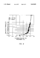
- FIG. 9 illustrates the threshold voltage (VT) distribution of EPROM cells before and after being baked at 250° C. for 500 hours.
- FIG. 10 illustrates the distribution of dies about ⁇ VT min , where ⁇ VT min is defined as the change in the minimum VT for an array of dies before and after baking.
- the present invention relates to an oxide/nitride/oxide (ONO) composite dielectric in which the nitride layer is thinner than either the top or bottom oxide layer in the resulting composite, and, in some instances, is eliminated from the composite.
- ONO composite dielectric of the present invention represents a significant deviation from prior art ONO composite dielectrics where the nitride layer is generally thicker than at least one of the surrounding oxide layers.
- Table 1 lists several prior art ONO composites as well as the preferred ONO composite of the present invention. As can be seen from Table 1, the requirement that both oxide layers be thicker than the middle nitride layer distinguishes the ONO composition of the present invention.
- the ONO composite of the present invention By designing the ONO composite of the present invention such that the nitride layer is thinner than either oxide layer, charge loss caused by electrons being trapped in the nitride layer is reduced. Charge loss arising from electron conductance in the nitride layer by electrons trapped in the nitride layer is also reduced. As a result, the ONO composite of the present invention provides enhanced charge retention and threshold voltage (VT) stability over prior art ONO composites.
- the ONO composite of the present invention is intended for use as an interpoly dielectric in nonvolatile memory cells such as EPROM, EEPROM, flash EPROM and flash EEPROM devices.
- the ONO composite 10 includes a bottom silicon dioxide layer 12 which is sufficiently thick to prevent hot electrons introduced into the floating gate from traversing the layer and becoming trapped at the interface between the top silicon dioxide layer 16 and the silicon nitride layer 14.
- the minimum required thickness for the bottom oxide layer 12 depends on the integrity of the bottom oxide layer and the ability of the bottom oxide layer to conform to the topology of the underlying poly surface to provide a bottom oxide layer with an uniform thickness. Whether the bottom oxide layer possesses these features depends on the method by which the bottom oxide layer is formed.
- the bottom oxide layer 12 may be deposited on the floating gate 18 of the cell by a variety of methods known in the art including, for example, thermal growth in a O 2 ambient environment, thermal growth in a N 2 O ambient environment, low temperature chemical vapor deposition (400° C.) and high temperature chemical vapor deposition (800-1000° C.). It is preferred that the bottom silicon dioxide layer 12 be deposited by high temperature chemical vapor deposition which produces an oxide film with a low concentration of defects which conforms to the surface of the underlying poly layer.
- the bottom silicon dioxide layer 12 preferably has a thickness of between about 25 and 100 ⁇ .
- the silicon nitride layer 14 used in the ONO composite of the present invention should be thinner than either the bottom 12 or top 16 oxide layers in the resulting composite. It is possible for the nitride layer to be thicker when deposited than either the top and/or bottom oxide layers. However, during further processing steps, such as oxidation of the nitride layer, the nitride layer should be made to be thinner than either oxide layer once the entire composite has been completed. Upon completion of the composite, the nitride layer preferably has a thickness equal to or less than about 80 ⁇ . Functionally, the nitride layer 14 need only be sufficiently thick for the resulting ONO composite to resist the electric field created during nonvolatile memory device operation and exhibit satisfactory charge retention. In instances where the top and/or bottom silicon dioxide layer has a high level of integrity, for example, when formed by high temperature chemical vapor deposition, the silicon nitride layer may be excluded.
- the silicon nitride layer 14 may be deposited on the bottom oxide layer 12 by a variety of methods known in the art including, for example, chemical vapor deposition and rapid thermal process (RTP).
- RTP rapid thermal process
- the nitride layer is preferably formed by chemical vapor deposition using SiH 2 Cl 2 /NH 3 at between 650°-780° C.
- the nitride layer may optionally be thermally treated at temperatures between 800°-1000° C. under either an O 2 or N 2 O atmosphere. Thermal treatment may also be performed after all three layers of the composite have been deposited. Pinholes are commonly present to a significant degree in thin nitride layers. Thermal treatment of the nitride layer in the presence of oxygen serves to plug the pinholes in the thin nitride layer with oxygen, thereby enhancing the ability of resulting ONO composite to prevent charge leakage from the floating gate.
- the top oxide layer 16 of the ONO composite 10 should be thicker than the nitride layer 14 once the entire composite has been formed and preferably has a thickness of between about 40 and 100 ⁇ .
- the top oxide layer 16 serves to prevent the positive potential of the control gate from injecting holes into the floating gate during programming.
- the top oxide layer 16 also serves to prevent electrons trapped in the nitride layer 14 from traversing the top oxide layer 16 and leaking into the control gate 20, further preventing charge leakage from the floating gate.
- the top oxide layer 16 may be deposited on the nitride layer by a variety of methods known in the art including, for example, thermal growth in a O 2 ambient environment, thermal growth in a N 2 O ambient environment, low temperature chemical vapor deposition (400° C.) and high temperature chemical vapor deposition (800°-1000° C.).
- the capacitively measured effective oxide thickness of the dielectric layer be equal to or less than about 180 ⁇ .
- the top and bottom silicon dioxide layers are preferably formed by high temperature chemical vapor deposition. Formation of at least one of the oxide layers by high temperature chemical vapor deposition is preferred since it enables the number of processing steps needed for fabrication of the memory device-to be reduced since a gate oxide layer over circuitry in the periphery of the memory cells may simultaneously be formed by high temperature chemical vapor deposition.
- pinholes 22 present in the bottom 12 and top 16 oxide layers generally will not be in alignment with each other. As a result, charge leakage from the floating gate is effectively impeded.
- the nitride layer it is possible to eliminate the nitride layer entirely while maintaining satisfactory charge retention when the top and bottom oxide layers are formed with a sufficiently high degree of integrity. It is preferred that the nitride layer be eliminated and that a single oxide layer be used in the interest of simplifying the required processing steps. When a single oxide layer is employed, it is preferred that the single oxide layer have a capacitively measured effective oxide thickness of less than or equal to 180 ⁇ .
- the single oxide layer may be formed as a single layer by high temperature chemical vapor deposition. However, it is preferred that the oxide layer be formed as a top and a bottom layer of silicon dioxide. As illustrated in FIG. 3, by forming the top oxide layer independently of the bottom oxide layer, pinholes 22 present in the bottom 12 and top 16 oxide layers generally will not be in alignment with each other. As a result, charge leakage from the floating gate is effectively impeded.
- the oxide layers are each preferably formed by high temperature chemical vapor deposition.
- the bottom oxide layer may be formed by thermal growth in the presence of N 2 O at 800°-1000° C. for 20-120 minutes, afterwhich, a top oxide layer is deposited by high temperature chemical vapor deposition such that the resulting oxide layer has a a capacitively measured effective oxide thickness of less than or equal to 180 ⁇ .
- the oxide layer be thermally treated at temperatures between 800°-1000° C. under either an O 2 or N 2 O atmosphere to thermally anneal the oxide layer.
- the ONO composite is employed in a nonvolatile memory cell which includes source 11 and drain 13 regions formed on the surface of a n- or p- type semiconductor substrate 15 and an insulating layer 17 thermally grown on top of the source 11 and drain 13 regions.
- the floating gate 18 is positioned on the insulating layer 17, preferably after patterning, such that the insulating layer serves to insulate the floating gate from the source and drain regions.
- the ONO composite 10 is positioned on the floating gate 18 and the control gate 20 is positioned on the ONO composite 10.
- FIGS. 4-8 illustrate the process sequence for fabricating a preferred EPROM cell in which the ONO composite of the present invention is employed.
- FIG. 4 illustrates a first photoresist level 24 patterned to define region 26 of the field oxide 27 in which an active device is to be formed.
- the first photoresist level 24 and underlying nitride layer 28 have been removed exposing the sacrificial oxide 31.
- An n-type enhancement implant, indicated by arrows 29 is then performed on region 26, e.g. 4.2 ⁇ 10 12 per square centimeter of boron at an energy of 50 keV.
- a photomasking process is used to define the floating gates 32, and n+ source and drain diffusion regions.
- photomask layers 28 and 30 are defined to protect the floating gate regions in poly one 32.
- the poly one 32 and thin nitride layers 34 are etched away except as protected by photomask layers 28 and 30 to expose the source and drain regions.
- n-type dopants indicated by arrows 36, are implanted in p-substrate 38 within the exposed regions. These regions are therefore self-aligned to floating gate 32 and to the field oxide regions 42 and 44.
- the substrate is annealed to activate the dopants and define the drain diffusion regions 46 and 48 and the source diffusion region 50. Also, drain oxides 52 and 54 and source oxide 56 are grown, along with oxides 58 covering the sides of the floating gate poly 32.
- An ONO composite 62 is then deposited over the floating gate poly 32.
- a bottom oxide layer 64 of about 65 ⁇ is deposited by high temperature chemical vapor deposition (pressure: 0.4 torr, 800° C., atmosphere: N 2 O (180 sccm) SiH 2 Cl 2 (90 sccm), time: 42 min.).
- a thin nitride layer 66 of about 55 ⁇ is then deposited over the bottom oxide layer 64 by high temperature chemical vapor deposition (pressure: 0.5 torr, 700° C., atmosphere: NH 3 (500 sccm) SiH 2 Cl 2 (50 sccm), time: 15 min.).
- the nitride layer 66 and bottom oxide layer 64 are then thermally treated under either an O 2 or N 2 O atmosphere at 800°-1000 C. for 30-180 minutes.
- a top oxide layer 68 of about 70 ⁇ is then deposited on the nitride layer by high temperature chemical vapor deposition (pressure: 0.4 torr, 800° C., atmosphere: N 2 O (180 seem) SiH 2 Cl 2 (90 sccm), time: 47 min.).
- a second poly layer 70 is deposited on top of the ONO composite 62 which serves as the control gate.
- a layer of tungsten silicide 72 is then deposited on the control gate (poly two) 70 which improves the conductivity of the wordlines.
- a photoresist layer 74 is then deposited on layer of tungsten silicide 72. The device is then etched to define the wordlines 76.
- EPROM cells formed as described above were tested for their charge retention performance by comparing the initial threshold voltage performance of a 4M EPROM device to the threshold voltage performance of the EPROM device after being baked at 250° C. for 168 and 500 hours.
- a threshold voltage VT
- the threshold voltage required to cause the cell to conduct decreases.
- FIG. 9 illustrates the threshold voltage (VT) distribution of dies before and after being baked at 250° C. for 500 hours.
- the average VT (VT average ) for this group of dies was 8.2 volts.
- the threshold voltage distribution for the dies does not change appreciably after a 500 hour bake.
- ⁇ VT VT min (bake hrs)VT min (initial).
- FIG. 10 thus illustrates that the VT min for an array of EPROM cells formed according to the present invention does not change significantly after baking at 250° C. for 168 hours and 500 hours.
- FIG. 10 further demonstrates the effectiveness of EPROM cells employing the ONO composite of the present invention to retain their charge.
Abstract
Description
              TABLE 1
______________________________________
               Bottom    Middle    Top
               Oxide     Nitride   Oxide
ONO Composite  Layer     Layer     Layer
______________________________________
Preferred Embodiment of
               25-100 Å
                         0-80 Å
                                   40-100 Å
the present invention.
U.S. Pat. No. 4,769,340
               200-250 Å
                         250 Å 30-50 Å
U.S. Pat. No. 4,720,323
               300 Å 150 Å 60 Å
U.S. Pat. No. 4,943,836
               100-200 Å
                         100-200 Å
                                   ≦15 Å
U.S. Pat. No. 4,613,956
               100 Å 200 Å 100 Å
U.S. Pat. No. 4,630,086
               15-50 Å
                         40-110 Å
                                   20 Å
U.S. Pat. No. 5,104,819
               ≦80 Å
                         50-120 Å
                                   50-150 Å
______________________________________
 * Oxide layers which are taught as being thinner than the nitride layer
 are indicated in underlined bold.
Claims (23)
Priority Applications (2)
| Application Number | Priority Date | Filing Date | Title |
|---|---|---|---|
| US08/315,209 US5619052A (en) | 1994-09-29 | 1994-09-29 | Interpoly dielectric structure in EEPROM device |
| US08/829,028 US5836772A (en) | 1994-09-29 | 1997-03-31 | Interpoly dielectric process |
Applications Claiming Priority (1)
| Application Number | Priority Date | Filing Date | Title |
|---|---|---|---|
| US08/315,209 US5619052A (en) | 1994-09-29 | 1994-09-29 | Interpoly dielectric structure in EEPROM device |
Related Child Applications (1)
| Application Number | Title | Priority Date | Filing Date |
|---|---|---|---|
| US08/829,028 Division US5836772A (en) | 1994-09-29 | 1997-03-31 | Interpoly dielectric process |
Publications (1)
| Publication Number | Publication Date |
|---|---|
| US5619052A true US5619052A (en) | 1997-04-08 |
Family
ID=23223374
Family Applications (2)
| Application Number | Title | Priority Date | Filing Date |
|---|---|---|---|
| US08/315,209 Expired - Lifetime US5619052A (en) | 1994-09-29 | 1994-09-29 | Interpoly dielectric structure in EEPROM device |
| US08/829,028 Expired - Lifetime US5836772A (en) | 1994-09-29 | 1997-03-31 | Interpoly dielectric process |
Family Applications After (1)
| Application Number | Title | Priority Date | Filing Date |
|---|---|---|---|
| US08/829,028 Expired - Lifetime US5836772A (en) | 1994-09-29 | 1997-03-31 | Interpoly dielectric process |
Country Status (1)
| Country | Link |
|---|---|
| US (2) | US5619052A (en) |
Cited By (34)
| Publication number | Priority date | Publication date | Assignee | Title |
|---|---|---|---|---|
| US5946569A (en) * | 1996-12-02 | 1999-08-31 | Taiwan Semiconductor Manufacturing Company, Ltd. | DRAM contact process by localized etch-stop removal |
| WO2000019504A2 (en) * | 1998-09-25 | 2000-04-06 | Conexant Systems, Inc. | Methods for fabricating interpoly dielectrics in non-volatile stacked-gate memory structures |
| US6051467A (en) * | 1998-04-02 | 2000-04-18 | Chartered Semiconductor Manufacturing, Ltd. | Method to fabricate a large planar area ONO interpoly dielectric in flash device |
| US6087695A (en) * | 1999-08-20 | 2000-07-11 | Worldwide Semiconductor Mfg | Source side injection flash EEPROM memory cell with dielectric pillar and operation |
| US6121092A (en) * | 1999-02-02 | 2000-09-19 | Macronix International Co., Ltd. | Silicide blocking process to form non-silicided regions on MOS devices |
| WO2000063958A1 (en) * | 1999-04-16 | 2000-10-26 | Advanced Micro Devices, Inc. | In situ, controlled ambient deposition of ono for application to flash eprom |
| US6153463A (en) * | 1999-07-09 | 2000-11-28 | Macronix International Co., Ltd. | Triple plate capacitor and method for manufacturing |
| US6180977B1 (en) * | 1997-12-04 | 2001-01-30 | Taiwan Semiconductor Manufacturing Company | Self-aligned edge implanted cell to reduce leakage current and improve program speed in split-gate flash |
| WO2001017031A1 (en) * | 1999-08-27 | 2001-03-08 | Macronix America, Inc. | Easy shrinkable novel non-volatile semiconductor memory cell utilizing split dielectric floating gate and method for making same |
| US6204529B1 (en) | 1999-08-27 | 2001-03-20 | Hsing Lan Lung | 8 bit per cell non-volatile semiconductor memory structure utilizing trench technology and dielectric floating gate |
| US6207990B1 (en) * | 1998-06-30 | 2001-03-27 | Stmicroelectronics, S.R.L. | Eeprom memory cell and corresponding manufacturing method |
| US6242773B1 (en) * | 1998-09-30 | 2001-06-05 | Advanced Micro Devices, Inc. | Self-aligning poly 1 ono dielectric for non-volatile memory |
| US6259140B1 (en) | 1999-02-02 | 2001-07-10 | Macronix International Co., Ltd. | Silicide blocking process to form non-silicided regions on MOS devices |
| US6274900B1 (en) * | 1998-01-05 | 2001-08-14 | Texas Instruments Incorporated | Semiconductor device architectures including UV transmissive nitride layers |
| US6395610B1 (en) | 1999-06-24 | 2002-05-28 | Lucent Technologies Inc. | Method of making bipolar transistor semiconductor device including graded, grown, high quality oxide layer |
| US6433383B1 (en) * | 1999-07-20 | 2002-08-13 | Advanced Micro Devices, Inc. | Methods and arrangements for forming a single interpoly dielectric layer in a semiconductor device |
| US6458677B1 (en) * | 1999-10-25 | 2002-10-01 | Advanced Micro Devices, Inc. | Process for fabricating an ONO structure |
| US6495475B2 (en) | 2001-03-28 | 2002-12-17 | Atmel Corporation | Method for fabrication of a high capacitance interpoly dielectric |
| US6509230B1 (en) | 1999-06-24 | 2003-01-21 | Lucent Technologies Inc. | Non-volatile memory semiconductor device including a graded, grown, high quality oxide layer and associated methods |
| US6521496B1 (en) * | 1999-06-24 | 2003-02-18 | Lucent Technologies Inc. | Non-volatile memory semiconductor device including a graded, grown, high quality control gate oxide layer and associated methods |
| US6551946B1 (en) | 1999-06-24 | 2003-04-22 | Agere Systems Inc. | Two-step oxidation process for oxidizing a silicon substrate wherein the first step is carried out at a temperature below the viscoelastic temperature of silicon dioxide and the second step is carried out at a temperature above the viscoelastic temperature |
| US6610614B2 (en) * | 2001-06-20 | 2003-08-26 | Texas Instruments Incorporated | Method for uniform nitridization of ultra-thin silicon dioxide layers in transistor gates |
| US6630392B2 (en) * | 2001-06-29 | 2003-10-07 | Hynix Semiconductor Inc. | Method for fabricating flash memory device |
| US6639271B1 (en) | 2001-12-20 | 2003-10-28 | Advanced Micro Devices, Inc. | Fully isolated dielectric memory cell structure for a dual bit nitride storage device and process for making same |
| US20030232507A1 (en) * | 2002-06-12 | 2003-12-18 | Macronix International Co., Ltd. | Method for fabricating a semiconductor device having an ONO film |
| US20030235957A1 (en) * | 2002-06-25 | 2003-12-25 | Samir Chaudhry | Method and structure for graded gate oxides on vertical and non-planar surfaces |
| US6670242B1 (en) | 1999-06-24 | 2003-12-30 | Agere Systems Inc. | Method for making an integrated circuit device including a graded, grown, high quality gate oxide layer and a nitride layer |
| US20040070365A1 (en) * | 2002-09-27 | 2004-04-15 | Chien-Liang Chiu | Portable labor-saving battery device for electric vehicle |
| US6744116B1 (en) * | 1998-06-30 | 2004-06-01 | Intel Corporation | Thin film using non-thermal techniques |
| US6753568B1 (en) * | 1996-11-15 | 2004-06-22 | Hitachi, Ltd. | Memory device |
| US7001807B1 (en) | 2001-12-20 | 2006-02-21 | Advanced Micro Devices, Inc. | Fully isolated dielectric memory cell structure for a dual bit nitride storage device and process for making same |
| US20060081908A1 (en) * | 2004-10-14 | 2006-04-20 | Smayling Michael C | Flash gate stack notch to improve coupling ratio |
| US20080203461A1 (en) * | 2007-02-20 | 2008-08-28 | Jungo Inaba | Gate structure of nand flash memory having insulators each filled with between gate electrodes of adjacent memory cells and manufacturing method thereof |
| EP2834843A4 (en) * | 2012-10-31 | 2016-03-09 | Hewlett Packard Development Co | Memory cell that prevents charge loss |
Families Citing this family (45)
| Publication number | Priority date | Publication date | Assignee | Title |
|---|---|---|---|---|
| US6297096B1 (en) * | 1997-06-11 | 2001-10-02 | Saifun Semiconductors Ltd. | NROM fabrication method |
| IL125604A (en) | 1997-07-30 | 2004-03-28 | Saifun Semiconductors Ltd | Non-volatile electrically erasable and programmble semiconductor memory cell utilizing asymmetrical charge |
| US6768165B1 (en) | 1997-08-01 | 2004-07-27 | Saifun Semiconductors Ltd. | Two bit non-volatile electrically erasable and programmable semiconductor memory cell utilizing asymmetrical charge trapping |
| US6633496B2 (en) | 1997-12-12 | 2003-10-14 | Saifun Semiconductors Ltd. | Symmetric architecture for memory cells having widely spread metal bit lines |
| US6633499B1 (en) | 1997-12-12 | 2003-10-14 | Saifun Semiconductors Ltd. | Method for reducing voltage drops in symmetric array architectures |
| US6430077B1 (en) | 1997-12-12 | 2002-08-06 | Saifun Semiconductors Ltd. | Method for regulating read voltage level at the drain of a cell in a symmetric array |
| US6348711B1 (en) | 1998-05-20 | 2002-02-19 | Saifun Semiconductors Ltd. | NROM cell with self-aligned programming and erasure areas |
| US6215148B1 (en) | 1998-05-20 | 2001-04-10 | Saifun Semiconductors Ltd. | NROM cell with improved programming, erasing and cycling |
| US6355580B1 (en) | 1998-09-03 | 2002-03-12 | Micron Technology, Inc. | Ion-assisted oxidation methods and the resulting structures |
| US6103576A (en) * | 1999-04-13 | 2000-08-15 | Microchip Technology Incorporated | Dielectric layer of a memory cell having a stacked oxide sidewall and method of fabricating same |
| DE19926108C2 (en) | 1999-06-08 | 2001-06-28 | Infineon Technologies Ag | Non-volatile semiconductor memory cell with a metal oxide dielectric and method for its production |
| US6265268B1 (en) * | 1999-10-25 | 2001-07-24 | Advanced Micro Devices, Inc. | High temperature oxide deposition process for fabricating an ONO floating-gate electrode in a two bit EEPROM device |
| US6429063B1 (en) | 1999-10-26 | 2002-08-06 | Saifun Semiconductors Ltd. | NROM cell with generally decoupled primary and secondary injection |
| CN1309426A (en) * | 1999-11-12 | 2001-08-22 | 密克罗奇普技术公司 | Storage cell for voltage control of independent threshold and device and method for selecting grid |
| US6490204B2 (en) | 2000-05-04 | 2002-12-03 | Saifun Semiconductors Ltd. | Programming and erasing methods for a reference cell of an NROM array |
| US6396741B1 (en) | 2000-05-04 | 2002-05-28 | Saifun Semiconductors Ltd. | Programming of nonvolatile memory cells |
| US6709927B1 (en) * | 2000-08-11 | 2004-03-23 | Advanced Micro Devices, Inc. | Process for treating ONO dielectric film of a floating gate memory cell |
| US6614692B2 (en) | 2001-01-18 | 2003-09-02 | Saifun Semiconductors Ltd. | EEPROM array and method for operation thereof |
| TW476144B (en) * | 2001-02-02 | 2002-02-11 | Macronix Int Co Ltd | Non-volatile memory |
| US6584017B2 (en) | 2001-04-05 | 2003-06-24 | Saifun Semiconductors Ltd. | Method for programming a reference cell |
| US6677805B2 (en) | 2001-04-05 | 2004-01-13 | Saifun Semiconductors Ltd. | Charge pump stage with body effect minimization |
| US6636440B2 (en) | 2001-04-25 | 2003-10-21 | Saifun Semiconductors Ltd. | Method for operation of an EEPROM array, including refresh thereof |
| KR100396473B1 (en) * | 2001-05-29 | 2003-09-02 | 삼성전자주식회사 | Semiconductor memory device having floating gate and Method of manufacturing the same |
| US6643181B2 (en) | 2001-10-24 | 2003-11-04 | Saifun Semiconductors Ltd. | Method for erasing a memory cell |
| US7098107B2 (en) | 2001-11-19 | 2006-08-29 | Saifun Semiconductor Ltd. | Protective layer in memory device and method therefor |
| DE10158019C2 (en) * | 2001-11-27 | 2003-09-18 | Infineon Technologies Ag | Floating gate field effect transistor |
| US6885585B2 (en) * | 2001-12-20 | 2005-04-26 | Saifun Semiconductors Ltd. | NROM NOR array |
| US6583007B1 (en) | 2001-12-20 | 2003-06-24 | Saifun Semiconductors Ltd. | Reducing secondary injection effects |
| US6917544B2 (en) | 2002-07-10 | 2005-07-12 | Saifun Semiconductors Ltd. | Multiple use memory chip |
| US6826107B2 (en) | 2002-08-01 | 2004-11-30 | Saifun Semiconductors Ltd. | High voltage insertion in flash memory cards |
| US7136304B2 (en) | 2002-10-29 | 2006-11-14 | Saifun Semiconductor Ltd | Method, system and circuit for programming a non-volatile memory array |
| US7178004B2 (en) | 2003-01-31 | 2007-02-13 | Yan Polansky | Memory array programming circuit and a method for using the circuit |
| US6869843B2 (en) * | 2003-06-27 | 2005-03-22 | Macronix International Co., Ltd. | Non-volatile memory cell with dielectric spacers along sidewalls of a component stack, and method for forming same |
| US20050215074A1 (en) * | 2004-03-26 | 2005-09-29 | Fuja Shone | ONO formation method |
| KR100596484B1 (en) * | 2004-05-31 | 2006-07-03 | 삼성전자주식회사 | Method of Forming Insulator Layer and Method of Manufacturing Non-Volatile Memory Device Using the same |
| US7638850B2 (en) | 2004-10-14 | 2009-12-29 | Saifun Semiconductors Ltd. | Non-volatile memory structure and method of fabrication |
| US8053812B2 (en) | 2005-03-17 | 2011-11-08 | Spansion Israel Ltd | Contact in planar NROM technology |
| US7763935B2 (en) * | 2005-06-23 | 2010-07-27 | Macronix International Co., Ltd. | ONO formation of semiconductor memory device and method of fabricating the same |
| EP1746645A3 (en) | 2005-07-18 | 2009-01-21 | Saifun Semiconductors Ltd. | Memory array with sub-minimum feature size word line spacing and method of fabrication |
| US7668017B2 (en) | 2005-08-17 | 2010-02-23 | Saifun Semiconductors Ltd. | Method of erasing non-volatile memory cells |
| US7808818B2 (en) | 2006-01-12 | 2010-10-05 | Saifun Semiconductors Ltd. | Secondary injection for NROM |
| US7760554B2 (en) | 2006-02-21 | 2010-07-20 | Saifun Semiconductors Ltd. | NROM non-volatile memory and mode of operation |
| US7692961B2 (en) | 2006-02-21 | 2010-04-06 | Saifun Semiconductors Ltd. | Method, circuit and device for disturb-control of programming nonvolatile memory cells by hot-hole injection (HHI) and by channel hot-electron (CHE) injection |
| US8253452B2 (en) | 2006-02-21 | 2012-08-28 | Spansion Israel Ltd | Circuit and method for powering up an integrated circuit and an integrated circuit utilizing same |
| US7701779B2 (en) | 2006-04-27 | 2010-04-20 | Sajfun Semiconductors Ltd. | Method for programming a reference cell |
Citations (11)
| Publication number | Priority date | Publication date | Assignee | Title |
|---|---|---|---|---|
| US4577390A (en) * | 1983-02-23 | 1986-03-25 | Texas Instruments Incorporated | Fabrication of polysilicon to polysilicon capacitors with a composite dielectric layer |
| US4613956A (en) * | 1983-02-23 | 1986-09-23 | Texas Instruments Incorporated | Floating gate memory with improved dielectric |
| US4616402A (en) * | 1984-05-07 | 1986-10-14 | Kabushiki Kaisha Toshiba | Method of manufacturing a semiconductor device with a stacked-gate-electrode structure |
| US4630086A (en) * | 1982-09-24 | 1986-12-16 | Hitachi, Ltd. | Nonvolatile MNOS memory |
| US4720323A (en) * | 1984-12-07 | 1988-01-19 | Kabushiki Kaisha Toshiba | Method for manufacturing a semiconductor device |
| US4769340A (en) * | 1983-11-28 | 1988-09-06 | Exel Microelectronics, Inc. | Method for making electrically programmable memory device by doping the floating gate by implant |
| EP0294864A2 (en) * | 1987-06-11 | 1988-12-14 | STMicroelectronics S.r.l. | Fabrication process for electrically cancellable nonvolatile EPROM memory cells and the cell thus obtained |
| US4808261A (en) * | 1986-04-29 | 1989-02-28 | Sgs Microelettronica S.P.A. | Fabrication process for EPROM cells with oxide-nitride-oxide dielectric |
| US4926222A (en) * | 1977-04-06 | 1990-05-15 | Hitachi, Ltd. | Semiconductor memory device and a method of manufacturing the same |
| US4943836A (en) * | 1987-07-30 | 1990-07-24 | Kabushiki Kaisha Toshiba | Ultraviolet erasable nonvolatile semiconductor device |
| US5104819A (en) * | 1989-08-07 | 1992-04-14 | Intel Corporation | Fabrication of interpoly dielctric for EPROM-related technologies |
Family Cites Families (2)
| Publication number | Priority date | Publication date | Assignee | Title |
|---|---|---|---|---|
| US5496747A (en) * | 1993-08-02 | 1996-03-05 | United Microelectronics Corporation | Split-gate process for non-volatile memory |
| US5457061A (en) * | 1994-07-15 | 1995-10-10 | United Microelectronics Corporation | Method of making top floating-gate flash EEPROM structure |
-
1994
- 1994-09-29 US US08/315,209 patent/US5619052A/en not_active Expired - Lifetime
-
1997
- 1997-03-31 US US08/829,028 patent/US5836772A/en not_active Expired - Lifetime
Patent Citations (11)
| Publication number | Priority date | Publication date | Assignee | Title |
|---|---|---|---|---|
| US4926222A (en) * | 1977-04-06 | 1990-05-15 | Hitachi, Ltd. | Semiconductor memory device and a method of manufacturing the same |
| US4630086A (en) * | 1982-09-24 | 1986-12-16 | Hitachi, Ltd. | Nonvolatile MNOS memory |
| US4577390A (en) * | 1983-02-23 | 1986-03-25 | Texas Instruments Incorporated | Fabrication of polysilicon to polysilicon capacitors with a composite dielectric layer |
| US4613956A (en) * | 1983-02-23 | 1986-09-23 | Texas Instruments Incorporated | Floating gate memory with improved dielectric |
| US4769340A (en) * | 1983-11-28 | 1988-09-06 | Exel Microelectronics, Inc. | Method for making electrically programmable memory device by doping the floating gate by implant |
| US4616402A (en) * | 1984-05-07 | 1986-10-14 | Kabushiki Kaisha Toshiba | Method of manufacturing a semiconductor device with a stacked-gate-electrode structure |
| US4720323A (en) * | 1984-12-07 | 1988-01-19 | Kabushiki Kaisha Toshiba | Method for manufacturing a semiconductor device |
| US4808261A (en) * | 1986-04-29 | 1989-02-28 | Sgs Microelettronica S.P.A. | Fabrication process for EPROM cells with oxide-nitride-oxide dielectric |
| EP0294864A2 (en) * | 1987-06-11 | 1988-12-14 | STMicroelectronics S.r.l. | Fabrication process for electrically cancellable nonvolatile EPROM memory cells and the cell thus obtained |
| US4943836A (en) * | 1987-07-30 | 1990-07-24 | Kabushiki Kaisha Toshiba | Ultraviolet erasable nonvolatile semiconductor device |
| US5104819A (en) * | 1989-08-07 | 1992-04-14 | Intel Corporation | Fabrication of interpoly dielctric for EPROM-related technologies |
Non-Patent Citations (10)
| Title |
|---|
| D.J. DiMaria et al., "Interface Effects and High Conductivity in Oxides Grown from Polycrystalline Silicon", Applied Physics Letters, vol. 27, No. 9, Nov. 1, 1975, pp. 505-507. |
| D.J. DiMaria et al., Interface Effects and High Conductivity in Oxides Grown from Polycrystalline Silicon , Applied Physics Letters, vol. 27, No. 9, Nov. 1, 1975, pp. 505 507. * |
| Fukuda et al, IEEE Electron Dev. Lett. vol. 12 Nall Nov. 1991 "Novel N2 O-Oxynitridation . . . Films". |
| Fukuda et al, IEEE Electron Dev. Lett. vol. 12 Nall Nov. 1991 Novel N 2 O Oxynitridation . . . Films . * |
| Hori et al, IEEE Transactions on Elect. Dev. vol. 36 No. 2 Feb. 1989 "Electrical . . . Processing". |
| Hori et al, IEEE Transactions on Elect. Dev. vol. 36 No. 2 Feb. 1989 Electrical . . . Processing . * |
| S. Mori et al., "Poly-Oxide/Nitride/Oxide Structures for Highly Reliable EPROM Cells", VLSI Symposium Digest of Technical Papers (1984), pp. 40-41. |
| S. Mori et al., "Reliability Aspects of 100A Inter-Poly Dielectrics for HIRH Density VLSI's", IEEE 1986 Symposium on VLSI Technology, San Diego, May 28-30, pp. 71-72. |
| S. Mori et al., Poly Oxide/Nitride/Oxide Structures for Highly Reliable EPROM Cells , VLSI Symposium Digest of Technical Papers (1984), pp. 40 41. * |
| S. Mori et al., Reliability Aspects of 100A Inter Poly Dielectrics for HIRH Density VLSI s , IEEE 1986 Symposium on VLSI Technology, San Diego, May 28 30, pp. 71 72. * |
Cited By (47)
| Publication number | Priority date | Publication date | Assignee | Title |
|---|---|---|---|---|
| US6753568B1 (en) * | 1996-11-15 | 2004-06-22 | Hitachi, Ltd. | Memory device |
| US5946569A (en) * | 1996-12-02 | 1999-08-31 | Taiwan Semiconductor Manufacturing Company, Ltd. | DRAM contact process by localized etch-stop removal |
| US6180977B1 (en) * | 1997-12-04 | 2001-01-30 | Taiwan Semiconductor Manufacturing Company | Self-aligned edge implanted cell to reduce leakage current and improve program speed in split-gate flash |
| US6383870B2 (en) | 1998-01-05 | 2002-05-07 | Texas Instruments Incorporated | Semiconductor device architectures including UV transmissive nitride layers |
| US6274900B1 (en) * | 1998-01-05 | 2001-08-14 | Texas Instruments Incorporated | Semiconductor device architectures including UV transmissive nitride layers |
| US6051467A (en) * | 1998-04-02 | 2000-04-18 | Chartered Semiconductor Manufacturing, Ltd. | Method to fabricate a large planar area ONO interpoly dielectric in flash device |
| US6501122B1 (en) * | 1998-04-02 | 2002-12-31 | Chartered Semiconductor Manufacturing Ltd. | Flash device having a large planar area ono interpoly dielectric |
| US6207990B1 (en) * | 1998-06-30 | 2001-03-27 | Stmicroelectronics, S.R.L. | Eeprom memory cell and corresponding manufacturing method |
| US6548355B2 (en) | 1998-06-30 | 2003-04-15 | Stmicroelectronics S.R.L. | EEPROM memory cell and corresponding manufacturing method |
| US6744116B1 (en) * | 1998-06-30 | 2004-06-01 | Intel Corporation | Thin film using non-thermal techniques |
| WO2000019504A2 (en) * | 1998-09-25 | 2000-04-06 | Conexant Systems, Inc. | Methods for fabricating interpoly dielectrics in non-volatile stacked-gate memory structures |
| US6339000B1 (en) | 1998-09-25 | 2002-01-15 | Conexant Systems, Inc. | Method for fabricating interpoly dielectrics in non-volatile stacked-gate memory structures |
| WO2000019504A3 (en) * | 1998-09-25 | 2000-07-13 | Conexant Systems Inc | Methods for fabricating interpoly dielectrics in non-volatile stacked-gate memory structures |
| US6242773B1 (en) * | 1998-09-30 | 2001-06-05 | Advanced Micro Devices, Inc. | Self-aligning poly 1 ono dielectric for non-volatile memory |
| US6259140B1 (en) | 1999-02-02 | 2001-07-10 | Macronix International Co., Ltd. | Silicide blocking process to form non-silicided regions on MOS devices |
| US6121092A (en) * | 1999-02-02 | 2000-09-19 | Macronix International Co., Ltd. | Silicide blocking process to form non-silicided regions on MOS devices |
| WO2000063958A1 (en) * | 1999-04-16 | 2000-10-26 | Advanced Micro Devices, Inc. | In situ, controlled ambient deposition of ono for application to flash eprom |
| US6395610B1 (en) | 1999-06-24 | 2002-05-28 | Lucent Technologies Inc. | Method of making bipolar transistor semiconductor device including graded, grown, high quality oxide layer |
| US6509230B1 (en) | 1999-06-24 | 2003-01-21 | Lucent Technologies Inc. | Non-volatile memory semiconductor device including a graded, grown, high quality oxide layer and associated methods |
| US6670242B1 (en) | 1999-06-24 | 2003-12-30 | Agere Systems Inc. | Method for making an integrated circuit device including a graded, grown, high quality gate oxide layer and a nitride layer |
| US6551946B1 (en) | 1999-06-24 | 2003-04-22 | Agere Systems Inc. | Two-step oxidation process for oxidizing a silicon substrate wherein the first step is carried out at a temperature below the viscoelastic temperature of silicon dioxide and the second step is carried out at a temperature above the viscoelastic temperature |
| US6521496B1 (en) * | 1999-06-24 | 2003-02-18 | Lucent Technologies Inc. | Non-volatile memory semiconductor device including a graded, grown, high quality control gate oxide layer and associated methods |
| US6153463A (en) * | 1999-07-09 | 2000-11-28 | Macronix International Co., Ltd. | Triple plate capacitor and method for manufacturing |
| US6433383B1 (en) * | 1999-07-20 | 2002-08-13 | Advanced Micro Devices, Inc. | Methods and arrangements for forming a single interpoly dielectric layer in a semiconductor device |
| US6087695A (en) * | 1999-08-20 | 2000-07-11 | Worldwide Semiconductor Mfg | Source side injection flash EEPROM memory cell with dielectric pillar and operation |
| US6432782B1 (en) | 1999-08-27 | 2002-08-13 | Macronix International Co., Ltd. | 8 bit per cell non-volatile semiconductor memory structure utilizing trench technology and dielectric floating gate |
| WO2001017031A1 (en) * | 1999-08-27 | 2001-03-08 | Macronix America, Inc. | Easy shrinkable novel non-volatile semiconductor memory cell utilizing split dielectric floating gate and method for making same |
| US6204529B1 (en) | 1999-08-27 | 2001-03-20 | Hsing Lan Lung | 8 bit per cell non-volatile semiconductor memory structure utilizing trench technology and dielectric floating gate |
| US6458677B1 (en) * | 1999-10-25 | 2002-10-01 | Advanced Micro Devices, Inc. | Process for fabricating an ONO structure |
| US7169714B2 (en) | 2000-01-11 | 2007-01-30 | Agere Systems, Inc. | Method and structure for graded gate oxides on vertical and non-planar surfaces |
| US20050164516A1 (en) * | 2000-01-11 | 2005-07-28 | Agere Systems Inc. | Method and structure for graded gate oxides on vertical and non-planar surfaces |
| US6495475B2 (en) | 2001-03-28 | 2002-12-17 | Atmel Corporation | Method for fabrication of a high capacitance interpoly dielectric |
| US6610614B2 (en) * | 2001-06-20 | 2003-08-26 | Texas Instruments Incorporated | Method for uniform nitridization of ultra-thin silicon dioxide layers in transistor gates |
| US6630392B2 (en) * | 2001-06-29 | 2003-10-07 | Hynix Semiconductor Inc. | Method for fabricating flash memory device |
| US6639271B1 (en) | 2001-12-20 | 2003-10-28 | Advanced Micro Devices, Inc. | Fully isolated dielectric memory cell structure for a dual bit nitride storage device and process for making same |
| US20040021172A1 (en) * | 2001-12-20 | 2004-02-05 | Advanced Micro Devices, Inc. | Fully isolated dielectric memory cell structure for a dual bit nitride storage device and process for making same |
| US6861307B2 (en) | 2001-12-20 | 2005-03-01 | Advanced Micro Devices, Inc. | Fully isolated dielectric memory cell structure for a dual bit nitride storage device and process for making same |
| US7001807B1 (en) | 2001-12-20 | 2006-02-21 | Advanced Micro Devices, Inc. | Fully isolated dielectric memory cell structure for a dual bit nitride storage device and process for making same |
| US20030232507A1 (en) * | 2002-06-12 | 2003-12-18 | Macronix International Co., Ltd. | Method for fabricating a semiconductor device having an ONO film |
| US20030235957A1 (en) * | 2002-06-25 | 2003-12-25 | Samir Chaudhry | Method and structure for graded gate oxides on vertical and non-planar surfaces |
| US20040070365A1 (en) * | 2002-09-27 | 2004-04-15 | Chien-Liang Chiu | Portable labor-saving battery device for electric vehicle |
| US20060081908A1 (en) * | 2004-10-14 | 2006-04-20 | Smayling Michael C | Flash gate stack notch to improve coupling ratio |
| US20080203461A1 (en) * | 2007-02-20 | 2008-08-28 | Jungo Inaba | Gate structure of nand flash memory having insulators each filled with between gate electrodes of adjacent memory cells and manufacturing method thereof |
| EP2834843A4 (en) * | 2012-10-31 | 2016-03-09 | Hewlett Packard Development Co | Memory cell that prevents charge loss |
| US9559106B2 (en) | 2012-10-31 | 2017-01-31 | Hewlett-Packard Development Company, L.P. | Memory cell that prevents charge loss |
| CN104247017B (en) * | 2012-10-31 | 2017-11-14 | 惠普发展公司,有限责任合伙企业 | The memory cell for preventing electric charge from losing |
| US10319728B2 (en) | 2012-10-31 | 2019-06-11 | Hewlett-Packard Development Company, L.P. | Fluid ejection devices comprising memory cells |
Also Published As
| Publication number | Publication date |
|---|---|
| US5836772A (en) | 1998-11-17 |
Similar Documents
| Publication | Publication Date | Title |
|---|---|---|
| US5619052A (en) | Interpoly dielectric structure in EEPROM device | |
| KR100644397B1 (en) | Method of Treating Thin Layer and Method of Manufacturing Non-Volatile Memory Cell Using the same | |
| EP1338034B1 (en) | Simultaneous formation of charge storage and bitline for wordline isolation | |
| US6479859B2 (en) | Split gate flash memory with multiple self-alignments | |
| JP4885420B2 (en) | Source / drain implantation during ONO formation to improve isolation of SONOS type devices | |
| US5726087A (en) | Method of formation of semiconductor gate dielectric | |
| US6468865B1 (en) | Method of simultaneous formation of bitline isolation and periphery oxide | |
| US6380035B1 (en) | Poly tip formation and self-align source process for split-gate flash cell | |
| US20060246665A1 (en) | Manufacturing process of an interpoly dielectric structure for non-volatile semiconductor integrated memories | |
| JPH0690008A (en) | Eprom cell provided with interpoly-insulator capable of being easily scaled down and its manufacture | |
| US6538292B2 (en) | Twin bit cell flash memory device | |
| US20070269972A1 (en) | Method of manufacturing a semiconductor device | |
| US6046086A (en) | Method to improve the capacity of data retention and increase the coupling ratio of source to floating gate in split-gate flash | |
| US6420237B1 (en) | Method of manufacturing twin bit cell flash memory device | |
| US6143608A (en) | Barrier layer decreases nitrogen contamination of peripheral gate regions during tunnel oxide nitridation | |
| US6093607A (en) | Method of forming sharp beak of poly by oxygen/fluorine implant to improve erase speed for split-gate flash | |
| US6756634B2 (en) | Gated semiconductor assemblies | |
| US6893920B2 (en) | Method for forming a protective buffer layer for high temperature oxide processing | |
| US20080017910A1 (en) | Method of manufacturing flash semiconductor device | |
| US6025229A (en) | Method of fabricating split-gate source side injection flash memory array | |
| US20020187609A1 (en) | Non-volatile memory devices and methods of fabricating the same | |
| US6448138B1 (en) | Nonvolatile floating-gate memory devices, and process of fabrication | |
| JPH08125040A (en) | Interpoly composite and preparation thereof | |
| CN1468447A (en) | Non-volatile memory with source side boron implantation | |
| KR100997781B1 (en) | Method of manufacturing EEPROM device |
Legal Events
| Date | Code | Title | Description |
|---|---|---|---|
| AS | Assignment |
Owner name: MACRONIX INTERNATIONAL CO., LTD., CHINA Free format text: ASSIGNMENT OF ASSIGNORS INTEREST;ASSIGNORS:YUN, CHANG;SHONE, FUCHIA;HUANG, CHIN YI;AND OTHERS;REEL/FRAME:007234/0601 Effective date: 19941122 |
|
| STCF | Information on status: patent grant |
Free format text: PATENTED CASE |
|
| CC | Certificate of correction | ||
| FEPP | Fee payment procedure |
Free format text: PAYOR NUMBER ASSIGNED (ORIGINAL EVENT CODE: ASPN); ENTITY STATUS OF PATENT OWNER: LARGE ENTITY |
|
| FPAY | Fee payment |
Year of fee payment: 4 |
|
| REMI | Maintenance fee reminder mailed | ||
| FPAY | Fee payment |
Year of fee payment: 8 |
|
| FPAY | Fee payment |
Year of fee payment: 12 |