US5611942A - Method for producing tips for atomic force microscopes - Google Patents
Method for producing tips for atomic force microscopes Download PDFInfo
- Publication number
- US5611942A US5611942A US08/397,617 US39761795A US5611942A US 5611942 A US5611942 A US 5611942A US 39761795 A US39761795 A US 39761795A US 5611942 A US5611942 A US 5611942A
- Authority
- US
- United States
- Prior art keywords
- tip
- masks
- carbon
- method recited
- etching
- Prior art date
- Legal status (The legal status is an assumption and is not a legal conclusion. Google has not performed a legal analysis and makes no representation as to the accuracy of the status listed.)
- Expired - Fee Related
Links
- 238000004519 manufacturing process Methods 0.000 title description 4
- 238000000034 method Methods 0.000 claims abstract description 69
- OKTJSMMVPCPJKN-UHFFFAOYSA-N Carbon Chemical group [C] OKTJSMMVPCPJKN-UHFFFAOYSA-N 0.000 claims abstract description 39
- 229910052799 carbon Inorganic materials 0.000 claims abstract description 39
- 239000007787 solid Substances 0.000 claims abstract description 24
- 230000002093 peripheral effect Effects 0.000 claims abstract description 13
- 239000000463 material Substances 0.000 claims abstract description 12
- 230000008021 deposition Effects 0.000 claims abstract description 10
- 230000015572 biosynthetic process Effects 0.000 claims abstract description 6
- XUIMIQQOPSSXEZ-UHFFFAOYSA-N Silicon Chemical compound [Si] XUIMIQQOPSSXEZ-UHFFFAOYSA-N 0.000 claims description 41
- 229910052710 silicon Inorganic materials 0.000 claims description 40
- 239000010703 silicon Substances 0.000 claims description 40
- 238000005530 etching Methods 0.000 claims description 36
- 238000010894 electron beam technology Methods 0.000 claims description 15
- 238000005229 chemical vapour deposition Methods 0.000 claims description 10
- 238000000151 deposition Methods 0.000 claims description 9
- 238000001020 plasma etching Methods 0.000 claims description 8
- 238000001039 wet etching Methods 0.000 claims description 4
- 238000001312 dry etching Methods 0.000 claims description 3
- 239000002904 solvent Substances 0.000 claims description 3
- 230000001678 irradiating effect Effects 0.000 claims 4
- 238000007654 immersion Methods 0.000 claims 1
- 238000000992 sputter etching Methods 0.000 claims 1
- 239000000523 sample Substances 0.000 description 9
- 239000000758 substrate Substances 0.000 description 5
- 230000007423 decrease Effects 0.000 description 3
- 238000005516 engineering process Methods 0.000 description 3
- 235000012431 wafers Nutrition 0.000 description 3
- 230000001133 acceleration Effects 0.000 description 2
- 238000000354 decomposition reaction Methods 0.000 description 2
- 238000010884 ion-beam technique Methods 0.000 description 2
- 238000005259 measurement Methods 0.000 description 2
- 230000003287 optical effect Effects 0.000 description 2
- 125000002524 organometallic group Chemical group 0.000 description 2
- YCKRFDGAMUMZLT-UHFFFAOYSA-N Fluorine atom Chemical compound [F] YCKRFDGAMUMZLT-UHFFFAOYSA-N 0.000 description 1
- 238000010420 art technique Methods 0.000 description 1
- 238000004630 atomic force microscopy Methods 0.000 description 1
- 125000004432 carbon atom Chemical group C* 0.000 description 1
- 238000011109 contamination Methods 0.000 description 1
- 238000007796 conventional method Methods 0.000 description 1
- 238000013016 damping Methods 0.000 description 1
- 238000010586 diagram Methods 0.000 description 1
- 229910052731 fluorine Inorganic materials 0.000 description 1
- 239000011737 fluorine Substances 0.000 description 1
- 150000002222 fluorine compounds Chemical class 0.000 description 1
- 230000010354 integration Effects 0.000 description 1
- 230000002452 interceptive effect Effects 0.000 description 1
- 239000011159 matrix material Substances 0.000 description 1
- 239000002923 metal particle Substances 0.000 description 1
- 239000000203 mixture Substances 0.000 description 1
- 238000012986 modification Methods 0.000 description 1
- 230000004048 modification Effects 0.000 description 1
- 150000002894 organic compounds Chemical class 0.000 description 1
- 150000002902 organometallic compounds Chemical class 0.000 description 1
- 239000002245 particle Substances 0.000 description 1
- 230000001681 protective effect Effects 0.000 description 1
- 239000010453 quartz Substances 0.000 description 1
- 238000000926 separation method Methods 0.000 description 1
- VYPSYNLAJGMNEJ-UHFFFAOYSA-N silicon dioxide Inorganic materials O=[Si]=O VYPSYNLAJGMNEJ-UHFFFAOYSA-N 0.000 description 1
Images


Classifications
-
- G—PHYSICS
- G01—MEASURING; TESTING
- G01Q—SCANNING-PROBE TECHNIQUES OR APPARATUS; APPLICATIONS OF SCANNING-PROBE TECHNIQUES, e.g. SCANNING PROBE MICROSCOPY [SPM]
- G01Q60/00—Particular types of SPM [Scanning Probe Microscopy] or microscopes; Essential components thereof
- G01Q60/24—AFM [Atomic Force Microscopy] or apparatus therefor, e.g. AFM probes
- G01Q60/38—Probes, their manufacture, or their related instrumentation, e.g. holders
-
- B—PERFORMING OPERATIONS; TRANSPORTING
- B82—NANOTECHNOLOGY
- B82Y—SPECIFIC USES OR APPLICATIONS OF NANOSTRUCTURES; MEASUREMENT OR ANALYSIS OF NANOSTRUCTURES; MANUFACTURE OR TREATMENT OF NANOSTRUCTURES
- B82Y35/00—Methods or apparatus for measurement or analysis of nanostructures
-
- Y—GENERAL TAGGING OF NEW TECHNOLOGICAL DEVELOPMENTS; GENERAL TAGGING OF CROSS-SECTIONAL TECHNOLOGIES SPANNING OVER SEVERAL SECTIONS OF THE IPC; TECHNICAL SUBJECTS COVERED BY FORMER USPC CROSS-REFERENCE ART COLLECTIONS [XRACs] AND DIGESTS
- Y10—TECHNICAL SUBJECTS COVERED BY FORMER USPC
- Y10S—TECHNICAL SUBJECTS COVERED BY FORMER USPC CROSS-REFERENCE ART COLLECTIONS [XRACs] AND DIGESTS
- Y10S438/00—Semiconductor device manufacturing: process
- Y10S438/978—Semiconductor device manufacturing: process forming tapered edges on substrate or adjacent layers
-
- Y—GENERAL TAGGING OF NEW TECHNOLOGICAL DEVELOPMENTS; GENERAL TAGGING OF CROSS-SECTIONAL TECHNOLOGIES SPANNING OVER SEVERAL SECTIONS OF THE IPC; TECHNICAL SUBJECTS COVERED BY FORMER USPC CROSS-REFERENCE ART COLLECTIONS [XRACs] AND DIGESTS
- Y10—TECHNICAL SUBJECTS COVERED BY FORMER USPC
- Y10S—TECHNICAL SUBJECTS COVERED BY FORMER USPC CROSS-REFERENCE ART COLLECTIONS [XRACs] AND DIGESTS
- Y10S977/00—Nanotechnology
- Y10S977/84—Manufacture, treatment, or detection of nanostructure
- Y10S977/849—Manufacture, treatment, or detection of nanostructure with scanning probe
- Y10S977/86—Scanning probe structure
- Y10S977/875—Scanning probe structure with tip detail
- Y10S977/878—Shape/taper
Definitions
- the present invention is directed to a method of producing silicon tips for use in atomic force microscope (AFM) technology, and in particular, to a method of producing three-point AFM tips.
- AFM atomic force microscope
- Atomic force microscopy is a technique for measuring extremely small dimensions, which takes advantage of the small forces created between the extreme end of an ultrafine tip and a surface which is to be measured or profiled.
- AFM may be used in the production of integrated circuit (IC) chips to measure the critical dimensions of the various components of the circuit, for example, the linewidth of the features of the IC wafer.
- This technique is known as AFM micrometrology and is becoming of increasing importance since as the scale of integration increases, there is a corresponding decrease in the dimensions of the features of the IC wafer which must be measured or profiled.
- AFM makes use of ultrafine tips which are mounted on spring-like cantilevers. As the tip is brought closer to the surface which is being profiled, the force between the surface and the tip causes the tip to deflect the cantilever. The degree of deflection may be measured to resolve the features of the surface.
- a conventional tip such as parabolic tip 1 shown in FIG. 1a loses resolution as the radius of the probe increases with depth, leaving a "dead zone" between the lower regions of the tip and the inner edge of the trench, which results in a loss of information about the inner edge of the trench.
- Conventional needle tips such as tips 3 shown in FIG. 1b provide better resolution. However, needle tips are extremely vulnerable to being damaged or broken, for example, due to crashes with the vertical edges of the trench.
- tip 5 is disposed in a trench.
- Such tips may be vibrated in two dimensions using piezo-electric elements, with the tip held stationary except for the vibration, and the surface to be profiled moved towards the tip.
- the tip vibration is damped. Damping of the vibration is therefore indicative that the surface of the trench is a certain distance from the tip at that particular location of the trench.
- the relative depth of the trench at different locations can be determined to obtain a surface profile.
- tips 5 In order to use this technique, tips 5 must have three points, one each for sensing the bottom surface and the right and left edges.
- the overall width w of the tip determines the smallest trench width which may be measured, the longitudinal distance d from the widest point of the tip to the bottom of the tip measures how close to the bottom of a trench a width can be measured, and the lateral distance D between the location of the tip at its widest extent and the location of the tip at its narrowest extent determines the limit of undercut which can be determined accurately. The smaller these dimensions can be made, the more accurate the resulting profile.
- substrate 10 is disposed in an evacuated chamber of a conventional electron beam unit.
- An organo-metallic compound gas stream is introduced into the chamber, and electron beam 12 is applied to forward surface 14 of silicon substrate 10.
- Electron beam 12 causes decomposition of the gas, and preferential deposition of the decomposed products onto surface 14.
- layers of the decomposed products build up on surface 14 to create tip 18.
- Tip 18 includes a carbon matrix in which metal particles are dispersed, that is, tip 18 is organo-metallic.
- FIG. 4e is a photomicrograph showing various three-point tips formed by using this prior art technique.
- the present invention is a method for forming a three point atomic force microscope tip.
- the method includes forming a substantially longitudinally extending solid tip having a peripheral surface and a forward end surface. Three masks are formed upon the solid tip, with a first and second of the masks formed along the peripheral surface, and a third of the masks formed on the forward end surface.
- the mask covered tip is then etched for a predetermined period of time to remove material from both the tip and the mask. After the predetermined period of time has elapsed, the masks are completely removed, and the removal of material from the tip results in the formation of three spikes which are pointed to the location from which the masks were removed.
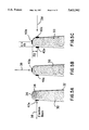
- FIGS. 1a and 1b are side views showing conventional AFM probes disposed in a trench.
- FIG. 2 is a side view showing a three-point AFM probe disposed in a trench.
- FIG. 3 is a perspective view showing a conventional silicon probe having a needle-shaped tip formed on the forward surface.
- FIGS. 4a-4d are side views showing formation of a three-point probe by a conventional CVD technique.
- FIG. 4e is a photomicrograph showing various three-point tips formed by using the prior art CVD technique.
- FIGS. 5a-5c are side views showing the carbon deposition step for forming a three-point probe according to the present invention.
- FIGS. 6a-6b are side views showing the etching step in forming a three-point probe according to the present invention.
- FIG. 7 is a side view of a three-point probe formed according to the present invention.
- FIG. 8 is a diagram of an apparatus used to deposit the masks according to the method of the present invention.
- FIG. 5a shows solid silicon tip 30 formed by conventional methods, for example, the microfabrication techniques discussed in the above-referenced article by Albrecht et at. These techniques for forming tip 30 do not form part of the present invention.
- Tip 30 has a circular peripheral surface which is tapered generally uniformly from base 32 to forward end 34 so as to give tip 30 a generally frustrum shape. The taper increases at end 34 so that tip 30 is rounded at forward end 34 into relatively flat forward end surface 36.
- the diameter of tip 30 is about 2,000 ⁇ at the base 32 and decreases slightly from the base 32 to the end 34 as shown in FIG. 5a.
- a carbon mask is formed on tip 30 by disposing tip 30 within the evacuated chamber of a conventional electron beam unit.
- the electron beam unit may be a conventional scanning electron microscope SEM adapted to include a gas supplier and a tilt stage.
- a volatile gas stream is introduced into the chamber.
- the gas must be an organic compound, and in a preferred embodiment is CF 4 .
- Electron beam 38 is turned on and impinges upon end 34 of tip 30 at a location near base surface 36. Beam 38 causes decomposition of the gas and deposition of the decomposed carbon onto the surface of tip 30.
- the carbon deposition occurs within the region irradiated by beam 38, and a radial distance out therefrom due to electron scatter from the surface.
- circular or disc-shaped carbon mask 40a is formed on the surface of tip 30 near end 34.
- the thickness and diameter of mask 40a will depend upon the diameter of the beam, the electron density, and the acceleration rate of the electrons, which further depends upon the applied voltage. Each of these variables will be controlled to form carbon mask 40a having the desired thickness and diameter. As explained below, the thickness and diameter of mask 40a and masks 40b and 40c ultimately will determine the final shape of the formed three-point tip.
- beam 38 has a diameter of less than 500 ⁇ , a primary beam acceleration voltage of 20 keV, a beam current of 30 pA, and impacts tip 30 at a location from end surface 36 which is approximately equal to the diameter of the beam, in this case, about 500 ⁇ .
- Beam 38 will be applied for a duration of approximately 15 minutes. Under these conditions, mask 40a will have a diameter slightly larger than that of the beam, for example, about 500 ⁇ , and a thickness of approximately 1 ⁇ .
- tip 30 is rotated so as to bring surface 36 into a position where it is perpendicular to beam 38, as shown in FIG. 5b. Tip 30 again is impinged upon by electron beam 38 to form disc-shaped carbon mask 40b on surface 36 of tip 30. Finally, tip 30 is rotated again so as to bring the surface of tip 30 opposite mask 40a into a position where it is perpendicular to beam 38, as shown in FIG. 5c. Tip 30 again is impinged upon by beam 38 to form mask 40c.
- each tip 30 will be subjected to electron beams having the same operating characteristics so as to form masks 40a-40c having the same diameters and widths.
- tip 30 is then etched to remove a predetermined quantity of the silicon.
- carbon masks 40a to 40c serve as protective coverings and preclude surface removal of the silicon at the locations of masks 40a to 40c. Instead, the silicon of tip 30 can be removed at these locations only by undercutting the surface of tip 30.
- the silicon near forward end 34 of tip 30 is removed in a parabolic manner at the location between masks 40a and 40b, and between masks 40b and 40c.
- end 34 of tip 30 is caused to have the general shape of a parabola extending between masks 40a and 40b, and between masks 40b and 40c such that the masks are undercut.
- a similar parabolic surface is created between mask 40a and 40c and the portion of tip 30 below these masks. As the etching proceeds, the surface is continually removed in a parabolic manner. As shown in FIG.
- the parabolic removal of silicon results in the creation of intermediate tip 130, having preliminary spikes 130a to 130c, which are centered upon masks 40a to 40c.
- the carbon atoms in masks 40a-c also are removed by the etching process, although at a much lower rate than the silicon.
- the thickness of masks 40a to 40c decreases as well.
- Three-point tip 230 includes tapered longitudinally extending section 231 including diamond-shaped head 231a.
- Spikes 230a and 230c extend outwardly from opposite sides of head 231a, along an axis which is substantially normal to the longitudinal axis of tapered section 231.
- Spike 230b extends substantially along the longitudinal axis of tapered section 231. All of masks 40a to 40c are removed by the etching process.
- Spikes 230a to 230c have points which generally correspond to the location of the centers of removed carbon masks 40a to 40c.
- Spikes 230a to 230c have a conical shape.
- the length of the spikes 230a and 230c are less than distance D2
- the length of spike 230b is less than distance D1.
- the final shape and dimensions will depend on the duration of the etching process, as well as the shape and dimensions of carbon masks 40a to 40c. These factors will be determined by one skilled in the art in dependence upon the desired shape and dimensions of tip 230 and spikes 230a to 230c.
- masks 40a to 40c will need to have a thickness of at least 1 ⁇ in order to withstand the etching process long enough to allow formation of spikes 230a to 230c.
- the masks may have a thickness of up to 10 ⁇ and still be removed entirely by the etching process.
- the etching may be performed by either a dry or wet etching process. However, the etching should be anisotropic so as to allow for greater etching rates at certain locations along tip 30.
- One suitable technique would be a conventional planar plasma etching process. Tip 30 having masks 40a to 40c would be disposed in a chamber filled with a reactive gas.
- the reactive gas would include a fluorine compound.
- An RF field is applied to the chamber to energize the reactive gas to the plasma state, in which the fluorine attacks the silicon and the carbon, converting it to volatile components which are removed from the chamber by the vacuum system.
- the plasma etching will be performed in the same chamber as the carbon deposition, with the same gas used for both deposition and etching, for example, CF 4 .
- the silicon and carbon could be removed by ion beam etching, in which the silicon atoms and carbon would be removed due to the impact of ionized gas particles upon the surface of the tip.
- Reactive ion etching which is a combination of plasma and ion beam etching also could be used.
- a wet etching process could be used, in which the carbon-masked tip would be immersed in or sprayed with a wet solvent.
- the solvent could be KOH.
- the final shape and dimensions of three-point tip 230 are determined by three factors: 1) the length of time the tip is subjected to the etching process; 2) the etching process used 3) the diameters and thicknesses of carbon masks 40a to 4c; and 4) the location of the masks on the tip.
- masks 40a to 40c will have a diameter of about 500 ⁇ and thickness of about 10 ⁇ , and the deposition and etching gas will be a mixture of CF 4 and O 2 having a volume ratio of 2.5:1, and the tip would be etched for a duration 15 seconds, depending on the particular conditions encountered during etching.
- a finished spike 230 formed according to the invention is shown disposed in a trench.
- the width w of the tip may be as small as 1,000 ⁇ , the distance d may be as small as 500 ⁇ , and the distance D may be as small 250 ⁇ . Accordingly, the use of a tip having these dimensions allows for a more accurate profile of the trench.
- CVD is used in the present invention, it is for the purpose of forming the masks, and is not used to create the finished spikes. Further, the carbon masks are substantially completely removed by the etching process. Accordingly, the present invention allows for formation of a finished three-point tip which is substantially free of carbon contamination. Further, the creation of spikes by removing silicon by etching may be controlled with greater accuracy than the creation of spikes by building up of deposited material. Thus, a three-point tip can be manufactured with greater accuracy so as to have smaller dimensions.
- An electron optical column 805 generates an electron beam 806 which impacts the tip 807 positioned on stage 808.
- the stage 808 has a rotation and tilt function which are used to position the tip 807 during etching to deposit the three masks 40a to 40c on the appropriate portion of the tip 807.
- Exhaust ports 809 and 810 are also provided from the shaft of electron optical column 805 and the etching chamber 803 respectively.
Abstract
Description
Claims (23)
Priority Applications (2)
| Application Number | Priority Date | Filing Date | Title |
|---|---|---|---|
| US08/397,617 US5611942A (en) | 1995-03-02 | 1995-03-02 | Method for producing tips for atomic force microscopes |
| JP04480596A JP3272935B2 (en) | 1995-03-02 | 1996-03-01 | Manufacturing method of chip for nuclear microscope |
Applications Claiming Priority (1)
| Application Number | Priority Date | Filing Date | Title |
|---|---|---|---|
| US08/397,617 US5611942A (en) | 1995-03-02 | 1995-03-02 | Method for producing tips for atomic force microscopes |
Publications (1)
| Publication Number | Publication Date |
|---|---|
| US5611942A true US5611942A (en) | 1997-03-18 |
Family
ID=23571942
Family Applications (1)
| Application Number | Title | Priority Date | Filing Date |
|---|---|---|---|
| US08/397,617 Expired - Fee Related US5611942A (en) | 1995-03-02 | 1995-03-02 | Method for producing tips for atomic force microscopes |
Country Status (2)
| Country | Link |
|---|---|
| US (1) | US5611942A (en) |
| JP (1) | JP3272935B2 (en) |
Cited By (29)
| Publication number | Priority date | Publication date | Assignee | Title |
|---|---|---|---|---|
| US5945678A (en) * | 1996-05-21 | 1999-08-31 | Hamamatsu Photonics K.K. | Ionizing analysis apparatus |
| US6091124A (en) * | 1996-06-13 | 2000-07-18 | International Business Machines Corporation | Micromechanical sensor for AFM/STM profilometry |
| US6246054B1 (en) * | 1997-06-10 | 2001-06-12 | Olympus Optical Co., Ltd. | Scanning probe microscope suitable for observing the sidewalls of steps in a specimen and measuring the tilt angle of the sidewalls |
| US6437329B1 (en) | 1999-10-27 | 2002-08-20 | Advanced Micro Devices, Inc. | Use of carbon nanotubes as chemical sensors by incorporation of fluorescent molecules within the tube |
| US6455847B1 (en) | 2000-04-26 | 2002-09-24 | Advanced Micro Devices, Inc. | Carbon nanotube probes in atomic force microscope to detect partially open/closed contacts |
| US20020138049A1 (en) * | 1998-06-10 | 2002-09-26 | Allen Mark G. | Microneedle devices and methods of manufacture and use thereof |
| US6504151B1 (en) * | 2000-09-13 | 2003-01-07 | Fei Company | Wear coating applied to an atomic force probe tip |
| US6503231B1 (en) * | 1998-06-10 | 2003-01-07 | Georgia Tech Research Corporation | Microneedle device for transport of molecules across tissue |
| US20030095582A1 (en) * | 2000-12-21 | 2003-05-22 | Ackley Donald E. | Microneedle array systems |
| US20030135166A1 (en) * | 2001-09-28 | 2003-07-17 | Gonnelli Robert R. | Switchable microneedle arrays and systems and methods relating to same |
| US20030135158A1 (en) * | 2001-09-21 | 2003-07-17 | Gonnelli Robert R. | Gas pressure actuated microneedle arrays, and systems and methods relating to same |
| US20030135167A1 (en) * | 2001-09-19 | 2003-07-17 | Gonnelli Robert R. | Microneedles, microneedle arrays, and systems and methods relating to same |
| US20030135201A1 (en) * | 2001-09-28 | 2003-07-17 | Gonnelli Robert R. | Microneedle with membrane |
| US6611707B1 (en) | 1999-06-04 | 2003-08-26 | Georgia Tech Research Corporation | Microneedle drug delivery device |
| US6736984B2 (en) | 2001-05-17 | 2004-05-18 | Honeywell International Inc. | Non-mechanical fabrication of carbon-containing work pieces |
| US6743211B1 (en) | 1999-11-23 | 2004-06-01 | Georgia Tech Research Corporation | Devices and methods for enhanced microneedle penetration of biological barriers |
| US6861855B2 (en) * | 1999-12-13 | 2005-03-01 | Upsys Probe Technology Sas | High density interconnection test connector especially for verification of integrated circuits |
| US6864481B2 (en) * | 2001-12-04 | 2005-03-08 | Sii Nanotechnology Inc. | Probe for scanning probe microscope |
| US20050225336A1 (en) * | 2002-01-25 | 2005-10-13 | Akio Kojima | Probe card and method for manufacturing probe card |
| US20070025907A1 (en) * | 2005-05-18 | 2007-02-01 | National Research Council Of Canada And University Of Alberta | Nano-tip fabrication by spatially controlled etching |
| WO2008013919A2 (en) * | 2006-07-27 | 2008-01-31 | The Regents Of The University Of California | Sidewall tracing nanoprobes, method for making the same, and method for use |
| US7344499B1 (en) | 1998-06-10 | 2008-03-18 | Georgia Tech Research Corporation | Microneedle device for extraction and sensing of bodily fluids |
| US20080083270A1 (en) * | 1999-02-05 | 2008-04-10 | Vladimir Mancevski | Carbon nanotube detection system |
| US20090140148A1 (en) * | 2007-11-29 | 2009-06-04 | Electronics And Telecommunications Research Institute | Bolometer and method of manufacturing the same |
| US20100138964A1 (en) * | 2008-11-26 | 2010-06-03 | The Regents Of The University Of California | Probes for enhanced magnetic force microscopy resolution |
| WO2011038470A1 (en) | 2009-09-29 | 2011-04-07 | Amg Technology Ltd. | Sensors for scanning probe microscopy, method for three-dimensional measurement and method for manufacturing such sensors |
| WO2014169383A1 (en) * | 2013-04-18 | 2014-10-23 | Bo Cui | Method of fabricating nano-scale structures and nano-scale structures fabricated using the method |
| US9302903B2 (en) | 2000-12-14 | 2016-04-05 | Georgia Tech Research Corporation | Microneedle devices and production thereof |
| US10782313B2 (en) | 2017-01-31 | 2020-09-22 | Hangzhou Tanzhen Nanotech. Co., Ltd. | Method of fabricating nano-scale structures on the edge and nano-scale structures fabricated on the edge using the method |
Families Citing this family (1)
| Publication number | Priority date | Publication date | Assignee | Title |
|---|---|---|---|---|
| JP4521482B2 (en) | 2004-04-26 | 2010-08-11 | オリンパス株式会社 | SPM cantilever and manufacturing method thereof |
Citations (5)
| Publication number | Priority date | Publication date | Assignee | Title |
|---|---|---|---|---|
| US4968585A (en) * | 1989-06-20 | 1990-11-06 | The Board Of Trustees Of The Leland Stanford Jr. University | Microfabricated cantilever stylus with integrated conical tip |
| EP0413041A1 (en) * | 1989-08-16 | 1991-02-20 | International Business Machines Corporation | Method of producing micromechanical sensors for the AFM/STM profilometry and micromechanical AFM/STM sensor head |
| US5171992A (en) * | 1990-10-31 | 1992-12-15 | International Business Machines Corporation | Nanometer scale probe for an atomic force microscope, and method for making same |
| US5242541A (en) * | 1989-08-16 | 1993-09-07 | International Business Machines Corporation | Method of producing ultrafine silicon tips for the afm/stm profilometry |
| US5282924A (en) * | 1990-07-25 | 1994-02-01 | International Business Machines Corporation | Micromechanical sensor fabrication process |
-
1995
- 1995-03-02 US US08/397,617 patent/US5611942A/en not_active Expired - Fee Related
-
1996
- 1996-03-01 JP JP04480596A patent/JP3272935B2/en not_active Expired - Fee Related
Patent Citations (6)
| Publication number | Priority date | Publication date | Assignee | Title |
|---|---|---|---|---|
| US4968585A (en) * | 1989-06-20 | 1990-11-06 | The Board Of Trustees Of The Leland Stanford Jr. University | Microfabricated cantilever stylus with integrated conical tip |
| EP0413041A1 (en) * | 1989-08-16 | 1991-02-20 | International Business Machines Corporation | Method of producing micromechanical sensors for the AFM/STM profilometry and micromechanical AFM/STM sensor head |
| US5116462A (en) * | 1989-08-16 | 1992-05-26 | International Business Machines Corporation | Method of producing micromechanical sensors for the afm/stm profilometry |
| US5242541A (en) * | 1989-08-16 | 1993-09-07 | International Business Machines Corporation | Method of producing ultrafine silicon tips for the afm/stm profilometry |
| US5282924A (en) * | 1990-07-25 | 1994-02-01 | International Business Machines Corporation | Micromechanical sensor fabrication process |
| US5171992A (en) * | 1990-10-31 | 1992-12-15 | International Business Machines Corporation | Nanometer scale probe for an atomic force microscope, and method for making same |
Non-Patent Citations (2)
| Title |
|---|
| "Two-dimensional Atomic Force Microprobe Trench Metrology System", D. Nyyssonen et al., J. Vac. Sci. Technol., B 9(6), Nov./Dec. 1991, pp. 3612-3616. |
| Two dimensional Atomic Force Microprobe Trench Metrology System , D. Nyyssonen et al., J. Vac. Sci. Technol. , B 9(6), Nov./Dec. 1991, pp. 3612 3616. * |
Cited By (48)
| Publication number | Priority date | Publication date | Assignee | Title |
|---|---|---|---|---|
| US5945678A (en) * | 1996-05-21 | 1999-08-31 | Hamamatsu Photonics K.K. | Ionizing analysis apparatus |
| US6091124A (en) * | 1996-06-13 | 2000-07-18 | International Business Machines Corporation | Micromechanical sensor for AFM/STM profilometry |
| US6246054B1 (en) * | 1997-06-10 | 2001-06-12 | Olympus Optical Co., Ltd. | Scanning probe microscope suitable for observing the sidewalls of steps in a specimen and measuring the tilt angle of the sidewalls |
| US20100312191A1 (en) * | 1998-06-10 | 2010-12-09 | Georgia Tech Research Corporation | Microneedle Devices and Methods of Manufacture and Use Thereof |
| US7344499B1 (en) | 1998-06-10 | 2008-03-18 | Georgia Tech Research Corporation | Microneedle device for extraction and sensing of bodily fluids |
| US20020138049A1 (en) * | 1998-06-10 | 2002-09-26 | Allen Mark G. | Microneedle devices and methods of manufacture and use thereof |
| US6503231B1 (en) * | 1998-06-10 | 2003-01-07 | Georgia Tech Research Corporation | Microneedle device for transport of molecules across tissue |
| US8708966B2 (en) | 1998-06-10 | 2014-04-29 | Georgia Tech Research Corporation | Microneedle devices and methods of manufacture and use thereof |
| US20080083270A1 (en) * | 1999-02-05 | 2008-04-10 | Vladimir Mancevski | Carbon nanotube detection system |
| US7610797B2 (en) | 1999-02-05 | 2009-11-03 | Xidex Corporation | Carbon nanotube detection system |
| US8257324B2 (en) | 1999-06-04 | 2012-09-04 | Georgia Tech Research Corporation | Microneedle drug delivery device |
| US7226439B2 (en) | 1999-06-04 | 2007-06-05 | Georgia Tech Research Corporation | Microneedle drug delivery device |
| US6611707B1 (en) | 1999-06-04 | 2003-08-26 | Georgia Tech Research Corporation | Microneedle drug delivery device |
| US6437329B1 (en) | 1999-10-27 | 2002-08-20 | Advanced Micro Devices, Inc. | Use of carbon nanotubes as chemical sensors by incorporation of fluorescent molecules within the tube |
| US6743211B1 (en) | 1999-11-23 | 2004-06-01 | Georgia Tech Research Corporation | Devices and methods for enhanced microneedle penetration of biological barriers |
| US20050137531A1 (en) * | 1999-11-23 | 2005-06-23 | Prausnitz Mark R. | Devices and methods for enhanced microneedle penetration of biological barriers |
| US6861855B2 (en) * | 1999-12-13 | 2005-03-01 | Upsys Probe Technology Sas | High density interconnection test connector especially for verification of integrated circuits |
| US6455847B1 (en) | 2000-04-26 | 2002-09-24 | Advanced Micro Devices, Inc. | Carbon nanotube probes in atomic force microscope to detect partially open/closed contacts |
| US6504151B1 (en) * | 2000-09-13 | 2003-01-07 | Fei Company | Wear coating applied to an atomic force probe tip |
| US9302903B2 (en) | 2000-12-14 | 2016-04-05 | Georgia Tech Research Corporation | Microneedle devices and production thereof |
| US20030095582A1 (en) * | 2000-12-21 | 2003-05-22 | Ackley Donald E. | Microneedle array systems |
| US7027478B2 (en) | 2000-12-21 | 2006-04-11 | Biovalve Technologies, Inc. | Microneedle array systems |
| US6736984B2 (en) | 2001-05-17 | 2004-05-18 | Honeywell International Inc. | Non-mechanical fabrication of carbon-containing work pieces |
| US20030135167A1 (en) * | 2001-09-19 | 2003-07-17 | Gonnelli Robert R. | Microneedles, microneedle arrays, and systems and methods relating to same |
| US8361037B2 (en) | 2001-09-19 | 2013-01-29 | Valeritas, Inc. | Microneedles, microneedle arrays, and systems and methods relating to same |
| US8920375B2 (en) | 2001-09-21 | 2014-12-30 | Valeritas, Inc. | Gas pressure actuated microneedle arrays, and systems and methods relating to same |
| US20030135158A1 (en) * | 2001-09-21 | 2003-07-17 | Gonnelli Robert R. | Gas pressure actuated microneedle arrays, and systems and methods relating to same |
| US20050137536A1 (en) * | 2001-09-28 | 2005-06-23 | Gonnelli Robert R. | Microneedle with membrane |
| US20090043250A1 (en) * | 2001-09-28 | 2009-02-12 | Gonnelli Robert R | Microneedle with membrane |
| US20030135201A1 (en) * | 2001-09-28 | 2003-07-17 | Gonnelli Robert R. | Microneedle with membrane |
| US20030135166A1 (en) * | 2001-09-28 | 2003-07-17 | Gonnelli Robert R. | Switchable microneedle arrays and systems and methods relating to same |
| US6864481B2 (en) * | 2001-12-04 | 2005-03-08 | Sii Nanotechnology Inc. | Probe for scanning probe microscope |
| US7394265B2 (en) * | 2002-01-25 | 2008-07-01 | Advantest Corp. | Flat portions of a probe card flattened to have same vertical level with one another by compensating the unevenness of a substrate and each identical height needle being mounted on the corresponding flat portion through an adhesive |
| US20050225336A1 (en) * | 2002-01-25 | 2005-10-13 | Akio Kojima | Probe card and method for manufacturing probe card |
| US7431856B2 (en) * | 2005-05-18 | 2008-10-07 | National Research Council Of Canada | Nano-tip fabrication by spatially controlled etching |
| US20070025907A1 (en) * | 2005-05-18 | 2007-02-01 | National Research Council Of Canada And University Of Alberta | Nano-tip fabrication by spatially controlled etching |
| WO2008013919A2 (en) * | 2006-07-27 | 2008-01-31 | The Regents Of The University Of California | Sidewall tracing nanoprobes, method for making the same, and method for use |
| WO2008013919A3 (en) * | 2006-07-27 | 2008-11-20 | Univ California | Sidewall tracing nanoprobes, method for making the same, and method for use |
| US20090140148A1 (en) * | 2007-11-29 | 2009-06-04 | Electronics And Telecommunications Research Institute | Bolometer and method of manufacturing the same |
| US8214918B2 (en) * | 2008-11-26 | 2012-07-03 | The Regents Of The University Of California | Probes for enhanced magnetic force microscopy resolution |
| US20100138964A1 (en) * | 2008-11-26 | 2010-06-03 | The Regents Of The University Of California | Probes for enhanced magnetic force microscopy resolution |
| WO2011038470A1 (en) | 2009-09-29 | 2011-04-07 | Amg Technology Ltd. | Sensors for scanning probe microscopy, method for three-dimensional measurement and method for manufacturing such sensors |
| WO2014169383A1 (en) * | 2013-04-18 | 2014-10-23 | Bo Cui | Method of fabricating nano-scale structures and nano-scale structures fabricated using the method |
| CN105189821A (en) * | 2013-04-18 | 2015-12-23 | 崔波 | Method of fabricating nano-scale structures and nano-scale structures fabricated using the method |
| US20160068384A1 (en) * | 2013-04-18 | 2016-03-10 | Bo Cui | Method of fabricating nano-scale structures and nano-scale structures fabricated using the method |
| US9522821B2 (en) * | 2013-04-18 | 2016-12-20 | Bo Cui | Method of fabricating nano-scale structures and nano-scale structures fabricated using the method |
| CN105189821B (en) * | 2013-04-18 | 2018-01-26 | 崔波 | The manufacture method of nanoscale structures and the nanoscale structures manufactured using this method |
| US10782313B2 (en) | 2017-01-31 | 2020-09-22 | Hangzhou Tanzhen Nanotech. Co., Ltd. | Method of fabricating nano-scale structures on the edge and nano-scale structures fabricated on the edge using the method |
Also Published As
| Publication number | Publication date |
|---|---|
| JP3272935B2 (en) | 2002-04-08 |
| JPH08285872A (en) | 1996-11-01 |
Similar Documents
| Publication | Publication Date | Title |
|---|---|---|
| US5611942A (en) | Method for producing tips for atomic force microscopes | |
| US6864481B2 (en) | Probe for scanning probe microscope | |
| US5578745A (en) | Calibration standards for profilometers and methods of producing them | |
| Tseng | Recent developments in micromilling using focused ion beam technology | |
| US5455419A (en) | Micromechanical sensor and sensor fabrication process | |
| Schiffmann | Investigation of fabrication parameters for the electron-beam-induced deposition of contamination tips used in atomic force microscopy | |
| EP0413040B1 (en) | Method of producing ultrafine silicon tips for the afm/stm profilometry | |
| US5838005A (en) | Use of focused ion and electron beams for fabricating a sensor on a probe tip used for scanning multiprobe microscopy and the like | |
| US10026590B2 (en) | Fiducial design for tilted or glancing mill operations with a charged particle beam | |
| Lee et al. | Submicron Si trench profiling with an electron‐beam fabricated atomic force microscope tip | |
| CN101548366B (en) | Method of planarizing solid surface with gas cluster ion beam and solid surface planarizing apparatus | |
| Ximen et al. | Microfabrication of AFM tips using focused ion and electron beam techniques | |
| US7258901B1 (en) | Directed growth of nanotubes on a catalyst | |
| JP3015646B2 (en) | Phase shift mask defect repair method and defect repair device | |
| Fu et al. | Influence of the redeposition effect for focused ion beam 3D micromachining in silicon | |
| JP2944559B2 (en) | Method for manufacturing through-hole for beam current measurement | |
| US7032437B2 (en) | Directed growth of nanotubes on a catalyst | |
| Novikov et al. | Silicon test object of the linewidth of the nanometer range for SEM and AFM | |
| Gruber et al. | Nanostructures produced by cluster beam lithography | |
| Hu et al. | Novel approach to atomic force lithography | |
| US20060123894A1 (en) | SPM sensor | |
| Wang et al. | Etching characteristics of chromium thin films by an electron beam induced surface reaction | |
| JPH09162102A (en) | Alignment mark detecting method | |
| US6227519B1 (en) | Female mold substrate having a heat flowable layer, method to make the same, and method to make a microprobe tip using the female substrate | |
| Sexton et al. | Scanning tunneling microscopy of compact disk surfaces |
Legal Events
| Date | Code | Title | Description |
|---|---|---|---|
| AS | Assignment |
Owner name: KABUSHIKI KAISHA TOSHIBA, JAPAN Free format text: ASSIGNMENT OF ASSIGNORS INTEREST;ASSIGNORS:MITSUI, TADASHI;OKUMURA, KATSUYA;REEL/FRAME:007455/0449;SIGNING DATES FROM 19950328 TO 19950421 |
|
| FEPP | Fee payment procedure |
Free format text: PAYOR NUMBER ASSIGNED (ORIGINAL EVENT CODE: ASPN); ENTITY STATUS OF PATENT OWNER: LARGE ENTITY |
|
| FPAY | Fee payment |
Year of fee payment: 4 |
|
| FPAY | Fee payment |
Year of fee payment: 8 |
|
| FEPP | Fee payment procedure |
Free format text: PAYOR NUMBER ASSIGNED (ORIGINAL EVENT CODE: ASPN); ENTITY STATUS OF PATENT OWNER: LARGE ENTITY Free format text: PAYER NUMBER DE-ASSIGNED (ORIGINAL EVENT CODE: RMPN); ENTITY STATUS OF PATENT OWNER: LARGE ENTITY |
|
| REMI | Maintenance fee reminder mailed | ||
| LAPS | Lapse for failure to pay maintenance fees | ||
| STCH | Information on status: patent discontinuation |
Free format text: PATENT EXPIRED DUE TO NONPAYMENT OF MAINTENANCE FEES UNDER 37 CFR 1.362 |
|
| FP | Lapsed due to failure to pay maintenance fee |
Effective date: 20090318 |