US5608873A - Device and method for interprocessor communication using mailboxes owned by processor devices - Google Patents
Device and method for interprocessor communication using mailboxes owned by processor devices Download PDFInfo
- Publication number
- US5608873A US5608873A US08/675,217 US67521796A US5608873A US 5608873 A US5608873 A US 5608873A US 67521796 A US67521796 A US 67521796A US 5608873 A US5608873 A US 5608873A
- Authority
- US
- United States
- Prior art keywords
- processor device
- processor
- mailbox
- ram
- transmitting
- Prior art date
- Legal status (The legal status is an assumption and is not a legal conclusion. Google has not performed a legal analysis and makes no representation as to the accuracy of the status listed.)
- Expired - Lifetime
Links
Images


Classifications
-
- G—PHYSICS
- G06—COMPUTING; CALCULATING OR COUNTING
- G06F—ELECTRIC DIGITAL DATA PROCESSING
- G06F15/00—Digital computers in general; Data processing equipment in general
- G06F15/16—Combinations of two or more digital computers each having at least an arithmetic unit, a program unit and a register, e.g. for a simultaneous processing of several programs
- G06F15/163—Interprocessor communication
- G06F15/167—Interprocessor communication using a common memory, e.g. mailbox
Definitions
- the invention pertains generally to inter-processor communication, and, more particularly, to inter-processor communication via mailboxes.
- a processor device in a multi-processor system architecture needs a capability of transferring information to the other processor devices in the system.
- Various inter-processor communication approaches have been used, with varying degrees of success.
- One such approach utilizes a central memory for storing the information to be transferred.
- Each processor device has read-access and write-access to the central memory via a bus.
- Bus arbitration logic is used to allow each processor device read-access and write-access to the memory without bus collision or contention.
- the central memory is random access memory (RAM), used for storing the information which is passed between the processors.
- Burkhardt, Jr., et al. "Intercomputer Communication Control Apparatus and Method", U.S. Pat. No. 5,142,683, which discloses a mailbox communication method and apparatus in which multiple processors have access to a common memory.
- a processor desiring to send a message to another processor inserts the message into its own mailbox, along with the address of the other processor.
- the sending processor interrupts the receiving processor, which, in response to the interrupt, scans the mailboxes to find the mailbox containing receiving processor's address and reads the message. Since the processors access common memory via a common work station bus, one disadvantage is that overhead is required to deal with bus contention and collision.
- Burkhardt has another disadvantage, since communication paths may be tied up unless processors copy and clear mailbox information quickly.
- RAMs incorporate RAM cells as well as 2-bus arbitration logic on a single chip, and allow both processor devices read-access and write-access to all RAM cells.
- read information and write information is stored in the same RAM location. Thus, a way must be provided to prevent the write information from overwriting the read information.
- the sending processor device when a sending processor device has information to be sent to a receiving processor, the sending processor device must first check to determine if the receiving processor device has written information to the RAM. If the receiving processor device has written information to theRAM, then the sending processor device must read the RAM before writing the information to be sent to the receiving processor device. The checking which is necessary in this approach unfortunately decreases the possible speed of the inter-processor communication.
- a further object of this invention is to enhance inter-processor communication speed.
- Yet another object of this invention is to provide inter-processor communication wherein information sent by one processor device can be ignored by the receiving processor device without tying up communication paths.
- a feature of this invention is that it provides interprocessor communication in a multi-processor environment via a post office RAM, which allows each processor device read-access to mailboxes belonging to other processor devices, and write-access to its own mailbox, eliminating the need for complex bus arbitration logic.
- a receiving processor can override a sending processor, for example, when the sending processor is executing erroneously or when the receiving processor is performing a time-critical task which should not be interrupted.
- each processor device can communicate at its own speed without slowing down the other processor devices.
- Another advantage of the invention is that it also allows for smaller die sizes compared to conventional dual port RAM techniques.
- the apparatus comprises a post office including a plurality of mailboxes. Each of the mailboxes is owned by a processor device, and read-accessible by the other processor devices.
- a method of communication among a plurality of processor devices including a transmitting processor and a receiving processor.
- a post office with a plurality of mailboxes is utilized.
- a transmitting processor writes information into a predetermined one of the mailboxes in the post office.
- the transmitting processor signals a receiving processor.
- the receiving processor determines which of the processor devices signalled it.
- the receiving processor reads the information in the predetermined mailbox.
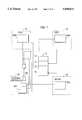
- FIG. 1 is a simplified block diagram of a post office RAM
- FIG. 2 is a detailed block diagram of a multi-processor system architecture with four processor devices utilizing the post office RAM for inter-processor communication;
- FIG. 3 is a block diagram illustrating communication between peer SSPs using a post office RAM
- FIG. 4 is a block diagram illustrating communication from an 80C186 to an SSP
- FIG. 5 is a block diagram illustrating communication from an SSP to an 80C186
- FIG. 6 is a block diagram illustrating communication from an external controller to an SSP and an 80C186;
- FIG. 7 is a block diagram illustrating communication from a mailbox to the external controller
- FIG. 8 shows one implementation of the post office RAM wherein each RAM cell is writable by one port and readable by all ports;
- FIG. 9 is a circuit diagram of the header port address of FIG. 8.
- FIG. 10 is a circuit diagram of the header port connection of FIG. 8;
- FIG. 11 is a circuit diagram of the POCON of FIG. 10;
- FIG. 12 is a circuit diagram of the post office block of FIG. 8;
- FIG. 13 is a circuit diagram of the post office register of FIG. 12.
- FIG. 14 is a circuit diagram of the post office bit of FIG. 13.
- FIG. 1 illustrates the general structure of the post office RAM 10.
- the post office RAM conveniently comprises a contiguous block of RAM.
- the block need not be contiguous; however, this is a practical implementation.
- the contiguous block of RAM includes a plurality of mailboxes 12, 14, 16, 18.
- the mailboxes 12, 14, 16, 18 are used to transfer information between the processor devices 20, 22, 24, 26 in a multi-processor system architecture.
- each mailbox 12, 14, 16, 18 may advantageously be eight contiguous bytes.
- the mailbox 12, 14, 16, 18 could be larger or smaller; the object is to obtain as much memory as practical without adversely impacting the die size. In any implementation, the desired area for memory must be balanced against the impact on the die size. Eight bytes is the favored balance for this implementation.
- Each of the mailboxes 12, 14, 16, 18 is owned by one of the processor devices 20, 22, 24, 26, termed an owner.
- the owner of a mailbox is allowed write-access to its own mailbox. All other processor devices are allowed read-access to the mailbox.
- a first mailbox 12 is owned by an external controller 20.
- the external controller 20 is the only device which has write-access to the first mailbox 12.
- the other processor devices, a streamlined signal processor 1 (SSP1) 22, a streamlined signal processor 2 (SSP2) 24, and a microprocessor 26, have read-access to the first mailbox 12 but may not write to mailbox 12.
- the owner of the mailbox may also have read-access to its own mailbox.
- a transmitting processor wishes to transfer data to another processor device, termed a receiving processor.
- the transmitting processor writes information to its own mailbox.
- the transmitting processor signals the receiving processor to read the transmitting processor's mailbox.
- the receiving processor may then read the transmitting processor's mailbox.
- Write-arbitration is maintained by permitting write-access to a mailbox by its owner, and prohibiting write-access to a mailbox by a processor device other than the mailbox's owner.
- one of the processor devices is an external control device 20. If, for example, the external control device 20 attempts a write-access to any mailbox of which it is not the owner, the write-access will be ignored by the mailbox. This may be implemented in the internal circuitry of the post office RAM. In this way, write-arbitration of the post office RAM is maintained without the usual latency and overhead associated with typical bus arbitration logic.
- the post office RAM 10 includes a multi-port RAM with a plurality of cells and a plurality of ports.
- the RAM is partitioned so that each processor device has a unique area of RAM to which it writes(its own mailbox), and therefore no write contention with another processor device is possible.
- Each cell is write-accessible by one of the ports.
- Each cell is read-accessible by all ports.
- Each port is utilized by one processor device.
- the bi-directional transfer of information between two processor devices takes place in the two different mailboxes owned by the two processor devices, each mailbox being a cell of the RAM.
- Each mailbox is allowed to be written by its owner.
- Information transmitted by one processor device is written to one cell of the RAM, and information received by that same processor is read from another cell of the RAM. Therefore, complex bus arbitration logic, which is ordinarily required to prevent write contention and to synchronize multiple processor device's write-accesses, is completely eliminated.
- each processor device owns its own mailbox, the processor devices can send information to each other without the latency required by typical dual-port RAM implementations, in which the read information and write information to be transferred is stored in the same RAM locations. No checking before writing is required to see if data in the RAM will be improperly overwritten. Nearly instantaneous bi-directional communication is thus achieved between the processor devices. Inter-processor speed improvements are achieved over the traditional dual-port RAM approach.
- the external controller 20 can write-access its own mailbox 12 at the same time that the other processor devices 22, 24 and 26 write-access their own mailboxes 14, 16, 18.
- each processor device can communicate without regard to the speed of the other processor devices.
- a transmitting processor can be ignored by the intended receiving processor without causing a system crash or a communication bottleneck.
- a system crash or communication bottleneck would deleteriously affect the other processor devices in the system.
- a receiving processor may override the transmitting processor by ignoring the information. This is useful in situations such as erroneous execution by the transmitting processor, or performance by the intended receiving processor of a time-critical task which cannot be interrupted.
- the implementation of the post office RAM shown here for four processor devices, can be expanded to handle additional processor devices. Also, a mailbox, here illustrated as eight bytes, can be expanded or reduced. The post office RAM can be reduced to handle fewer processor devices, if desired. The principles described herein still apply.
- FIG. 2 is a detailed block diagram of one embodiment of a multi-processor architecture utilizing a post office RAM for communication.
- a motion control or servo control architecture 100 incorporating a post office RAM 10 is shown generally in simplified block diagram format.
- the post office RAM 10 includes four mailboxes 12, 14, 16, 18.
- the four processor devices including a master microprocessor 26, SSP1 22, SSP2 24, and an external device (not illustrated) can access the post office RAM 10.
- the master microprocessor 26 is connected to its mailbox 18 over a first bus 104a.
- the master microprocessor 26 also provides address and data information to SSP1 22, SSP2 24 and the post office 10 over the first bus 104a.
- the first bus 104a also may transmit control information. Additionally, the first bus 104a may interface with parallel I/O 127, which in turn communicates via a general I/O bus 130. In the embodiment illustrated, the first bus 104a is a 16-bit A/D/C bus.
- SSP2 24 communicates with its mailbox 16 over a second bus 104b.
- SSP1 22 communicates with its mailbox 14 over a third bus 104c.
- the external device (not illustrated) communicates with its mailbox 12 via a header port on a fourth bus 104d.
- Each of the streamlined signal processors 22, 24 may be a microprogrammable processor, including a sequencer memory 116a, 116b, an instruction memory RAM 118a, 118b, an instruction memory ROM 120a, 120b and an execution unit. It will be known to those of ordinary skill in the art that such an execution unit could include an arithmetic logic unit, registers and related processing devices. Such a microprogrammable processor could be programmed with microcode.
- Each of the streamlined signal processors 22, 24 performs programmed tasks. In the illustrated servo control architecture, the streamlined signal processors 22, 24 communicate with appropriate peripherals and perform tasks related to servo loop control.
- FIG. 2 shows one example in which the post office RAM 10 is implemented as a plurality of contiguous RAM blocks.
- the post office RAM 10 is implemented as a plurality of contiguous RAM blocks.
- These four RAM blocks can be used for transferring information among the four processor devices in the system, the four processor devices being the microprocessor 26, SSP1 22, SSP2 24, and the external processor or controller connected to the header port.
- a first RAM block 18 is write-accessed by the microprocessor 26 through the bus 104a.
- SSP2 write-accesses a second RAM block 16 through a bus 104b.
- SSP1 write-accesses a third RAM block 14 through a bus 104c.
- the external processor connected to the header port accesses a fourth RAM block 12 through the bus 104d.
- the architecture also includes X-addressable RAM (XRAM) 112a, 112b and Y-addressable RAM(YRAM) 114a, 114b.
- XRAM X-addressable RAM
- YRAM Y-addressable RAM
- Each streamlined signal processor can access one of the XRAMs 112a, 112b, and YRAMs 114a, 114b.
- the master microprocessor 26 can also access the XRAMs 112a, 112b and YRAMs 114a, 114b via the first bus 104a.
- Each RAM block 12, 14, 16, 18 may be written by its owner, that is, one of the processor devices 22, 24, 26 or the external processor 20.
- the microprocessor 26 writes data to its RAM block 18, the streamlined signal processors 22, 24 write data to their RAMblocks 14, 16; and an external controller, such as an optical data channel controller, writes data to its RAM block 12.
- an external controller such as an optical data channel controller
- All of the processor devices can read all of the RAM blocks 12, 14, 16, 18. This facilitates transfer of data from one processor device to another.
- the processor device with the information to be transferred writes its data to its own RAM block.
- the transmitting processor then signals the receiving processor to read the transmitting processor's RAM block.
- SSP1 22 writes data to its RAM block 14 via the third bus 104c.
- SSP1 22 signals the microprocessor 26 to read SSP1's RAM block 14.
- the transmitting processor In order to communicate between two processor devices, the transmitting processor writes information into its mailbox in the post office RAM. The transmitting processor then signals the receiving processor. The receiving processor determines which processor signalled it, then reads the information in the transmitting processor's mailbox. The receiving processor then acts on the information. The exact signaling method depends on which processor device is signaling, and which processor device is being signaled.
- Peer communication refers to communication between similar processor devices (a peer).
- peer communication occurs when the SSPs communicate with each other.
- Each peer has at least one vector register 402a-d and trigger 404a-d pair, which are used in signalling.
- the vector register 402a-d preferably contains the start address of a subroutine.
- the subroutine preferably directs the processor device to read the mailbox 14, 16 in the post office RAM 10 which is owned by the other peer.
- the subroutine also directs the processor device to perform some task based on the information in the mailbox.
- the triggers 404a-d informs the processor device that it should execute the subroutine pointed to by the corresponding vector register 402a-d.
- a plurality of vector register 402a-d and trigger 404a-d pairs can be used to specify a peer to address one of a plurality of subroutines.
- the triggers 404a-d may be enabled by writing to a strobe location 403a having a unique address in a data space of the SSP 22, 24.
- the signalling SSP sets a latch by writing to the strobe's unique address in the data space.
- the signaled SSP enters an idle state, it detects the latch.
- the signaled SSP then advantageously branches immediately to the subroutine which is pointed to by the corresponding vector register 402a-d.
- the signaled SSP may send an acknowledgement back to the signalling SSP to indicate that the mailbox has been processed.
- the signaled SSP may simply return to the idle state to await other triggers caused by other processor devices.
- each SSP 22, 24 is provided with two pairs of asynchronous vector registers 402a-d and triggers 404a-d.
- the vector registers 402a-d and triggers 404a-d are used to direct the SSP to perform a task which is related to its peer SSP.
- Each of the two vector registers 402a-d (called SSP -- A and SSP -- B vector registers) is preferably programmed at power-up time with a start address of one of two subroutines that will be executed by the signaled SSP.
- the vector registers 402a-d may also be downloaded with the start address.
- the subroutines may contain microcode instructions which preferably direct the signaled SSP to read information from the appropriate mailbox, and subsequently to act on the information in the mailbox.
- An SSP signals its peer SSP to execute the subroutine pointed to by a vector register 402a-d by using its corresponding trigger 404a-d.
- Both trigger latches (called SSP -- A and SSP -- B triggers) are preferably cleared when the signaled SSP enters the idle state.
- SSP1 22 write-accesses its own mailbox 14, and writes some information to its mailbox 14.
- SSP1 22 signals SSP2 24 by way of a SSP1 -- A trigger 404a or a SSP1 -- B trigger 404b.
- SSP1 -- A trigger 404a causes SSP2 24 to execute a first subroutine pointed to by a SSP1 -- A vector register 402a.
- SSP1 -- B trigger 404b causes SSP2 24 to execute a second subroutine pointed to by a SSP1 -- B vector register 402b. Both subroutines cause SSP2 24 to read SSP1's mailbox 14.
- SSP2 24 writes information to its own mailbox 16.
- SSP2 24 signals SSP1 22 by way of a SSP2 -- A trigger 404c or a SSP2 -- B trigger 404d.
- SSP1 22 is in the idle state
- the SSP2 -- A trigger 404c causes SSP1 22 to execute a third subroutine pointed to by a SSP2 -- A vector register 402c.
- the SSP2 -- B trigger 404d causes SSP1 22 to execute a fourth subroutine pointed to by a SSP2 -- B vector register 402d. Both subroutines cause SSP1 22 to read SSP2's mailbox 16.
- FIG. 4 illustrates the master microprocessor communicating to one of the SSPs.
- the master microprocessor can communicate with the SSP in a manner similar to the above-described peer communication. That is, the master microprocessor can write to its own mailbox, and signal the SSP. The SSP can then read the master microprocessor's mailbox and act on the information.
- the master microprocessor is an 80C186 26.
- the 80C186 26 writes its mailbox 18 and signals an SSP 22, 24 to read the mailbox's contents.
- An 80C186 vector register 502 is provided for each SSP 22, 24, to allow the 80C186 26 to signal one of the SSPs 22, 24 to read the 80C186 mailbox 18.
- a memory-mapped trigger 504 (called 80C186 trigger) is provided for each SSP 22, 24.
- the trigger 504 may be a trigger latch with a unique address, which is provided in a data space of the 80C186.
- an SSP's 80C186 trigger latch is preferably set by the 80C186 26 writing to the trigger latch's unique address.
- the trigger latch is preferably cleared when the SSP enters the Idle State.
- SSP1's 80C186 trigger latch 504a is set when the 80C186 26 writes to its unique address.
- SSP2's 80C186 trigger latch 504b is set when the 80C186 26 writes to its unique address.
- SSP1 22 is in the idle state
- the presence of the SSP1 80C186 trigger latch 504a causes SSP1 22 to execute a subroutine pointed to by the corresponding SSP1 80C186 vector register 502a.
- SSP2 24 is in the idle state
- the presence of the SSP2 80C186 trigger latch 504b causes SSP2 24 to execute a second subroutine pointed to by the corresponding SSP2 80C186 vector register 502b.
- FIG. 5 illustrates SSP to master microprocessor communication.
- SSP signaling to the 80C186 is slightly different from the above-described communication, due to the differences in architecture of the master microprocessor. Since the 80C186 processor is based on interrupts rather than triggers and vector registers, the SSPs preferably use interrupts as a way of signaling the 80C186 that the mailbox has been written.
- interrupts for communication may be as follows.
- One of the SSPs 22, 24 can generate an interrupt, and the master microprocessor can execute a subroutine which determines which SSP generated the interrupt.
- the master microprocessor can read information in the mailbox owned by the SSP which generated the interrupt.
- the master microprocessor can act on the information which it read.
- an interrupt vector 602 and a corresponding interrupt service routine is programmed into a program memory space of the 80C186 before the system is powered-up.
- the interrupt vector contains the address of the ISR.
- the program memory space is advantageously EPROM.
- An SSP generates an interrupt to the 80C186 in a similar way as it generates a trigger to its peer SSP. The interrupt is generated when the SSP simply writes to a memory-mapped latch 606a, 606b, called a 80C186 interrupt strobe 606. Outputs 610a, 610b of each the latches 606a, 606b from both SSPs are OR-ed together to drive a 80C186 INT1 interrupt input pin 608.
- the output 610a, 610b of each of these latches from both SSPs is connected to a bit in an SSP status register 612 in the master microprocessor 26.
- the 80C186 can determine which SSP caused the interrupt.
- the INT1 ISR preferably contains instructions which direct the 80C186 to first read the SSP status register 612 to determine which of the SSPs 22, 24 caused the interrupt, next to read the mailbox 14, 16 owned by the indicated SSP 22, 24, and subsequently, to act on that information.
- the instructions may be in Assembly Language.
- the 80C186 interrupt strobe latch 606a, 606b is preferably cleared when the 80C186 reads the SSP status register 612.
- FIG. 6 illustrates communication of the external controller to the SSPs and the master microprocessor.
- the external controller signals the SSPs by way of a vector register and trigger pair in a manner similar to the master microprocessor (80C186)-to-SSP signaling.
- An EXT -- TRIG input pin is provided for each SSP.
- An external trigger latch 702 is set when the external controller pulses the EXT -- TRIG input pin for that SSP. Specifically, the external controller writes information to its mailbox 12.
- An EXT -- TRIG1 trigger 702a for SSP1 22 is set when the external controller pulses the EXT -- TRIG1 input pin; and an EXT -- TRIG2 trigger 702b for SSP2 24 is set when the external controller pulses the EXT -- TRIG2 input pin.
- the vector register EXT vector 704a, 704b corresponding to the trigger 702a, 702b contains the address of a subroutine which is preferably executed by the SSP. The subroutine preferably reads the information in the external controller's mailbox 12, and acts on that information.
- the external trigger latch 702a, 702b for an SSP 22, 24 is cleared when the SSP 22, 24 enters the idle state.
- the external controller can also communicate with the master microprocessor through the mailbox, as illustrated in FIG. 6. If the master microprocessor is an 80C186, it has a non-maskable interrupt (NMI) input pin 706. The external controller 20 signals the 80C186 26 directly via the 80C186 NMI input pin 706. An ISR is associated with the NMI.
- the NMI ISR contains instructions, preferably in Assembly Language, which preferably direct the 80C186 26 to read the information in the external controller mailbox 12, and subsequently to act on the information.
- FIG. 7 illustrates mailbox signalling to the external controller.
- the architecture makes no provision for mailbox signaling to the external controller, since the controller never needs to read the mailboxes 12, 14, 16, 18 in the particular application.
- it is appropriate to make no provisions for communication between processor devices which never communicate.
- Mailbox signalling to the external controller may optionally be provided as follows.
- the SSPs 22, 24 and 80C186 26 each have an additional memory-mapped trigger latch 892a, 892b, 892c for generating a trigger to the external controller 20.
- a trigger latch 892a, 892b, 892c is set when the processor device (SSP 22, 24 or 80C186 26) writes to the trigger latch's unique address in the processor's data space.
- the output of these three trigger latches 892a, 892b, 892c are OR-ed together to produce a single trigger 894 which is driven to the external controller via an external interrupt EXT -- INT output pin.
- each output of these three trigger latches is connected to one of three bits in mailbox status register 896.
- the external controller 20 can determine which of the other processor devices 22, 24, 26 generated the trigger.
- the EXT -- INT pin may be connected to an external interrupt pin on the external controller 20, or alternatively could be polled by the external controller 20 via an input port pin.
- the external controller 20 preferably executes a subroutine which instructs the external controller to first read the mailbox status register 806, next to read the information in the indicated processor's mailbox 14, 16, 18, and subsequently to act on that information.
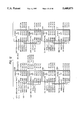
- FIG. 8 showing a block diagram of one implementation of the post office RAM.
- the illustrated embodiment includes four blocks of memory in the post office (POBLK) 822, 824, 826, 828, for the external controller (p -- head), SSP1 (p -- ssp1), SSP2 (p -- ssp2), and the master microprocessor (p -- c186), respectively. Also included are four post office connections (POCON or HPCON) 814, 816, 818, 820, corresponding to the header port for the external controller (c -- hport), SSP1 (c -- ssp1), SSP2 (c -- ssp2), and the master microprocessor (c -- c186), respectively. These post office connections provide address information and read/write control for each port.
- POBLK post office
- SSP1 p -- ssp1
- SSP2 p -- ssp2
- p -- c186 master microprocessor
- Each post office connection 814, 816, 818, 820 includes input address lines 830a-d, and a read line 832a-d.
- the header port connection 814 also includes an enable line 836.
- the master microprocessor connection 820 also includes a select line 838, which is connected to each of the read line 832d and write line 834c by a logical-AND connection.
- Each post office connection 814, 816, 818, 820 outputs a plurality of write lines (WR0, WR1, etc.) 802a, 802b, 802c and 802d and a plurality of read lines (RD0, RD1, etc.) 804a, 804b, 804c and 804d, respectively to post office blocks containing the data.
- the output write lines 802a, 802b, 802c and 802d from each of the post office connections 814, 816, 818, 820 connect to the corresponding post office block 822, 824, 826, 828.
- Address lines 802a consists of eight write lines WR0-WR7, one write line for each of eight bytes.
- post office connection 814 accesses data on a byte wide basis.
- Address lines 802b, 802c and 802d consist of 4 write lines. Each write line accesses two bytes of data.
- Post office connection 816, 818 and 820 access data on a word wide basis in the described embodiment, thus the difference in the number of write lines between the post office connections in the described embodiment.
- thirty two read lines 804a output from the header port connection, one for each of the thirty two bytes in the described embodiment.
- eight read lines are connected from the header port to each post office block 822, 824 826 and 828.
- the other ports 816, 818 and 820 output sixteen address lines 802b, 802c and 802d, four output read lines being input to each post office block.
- Each post office block 822,824,826,828 further includes data input/output lines (HPD, D0, D1, D2) 806, 808, 810, 812.
- HPD contains 16 bits of data and the remaining data I/O lines are 16 bits for each port. Potential write collisions are avoided since only one port has write access to its mailbox.
- FIG. 9 illustrates the header port address (HPA) 830a of FIG. 8.
- the HPA includes five bits (4:0).
- the zeroth, third and fourth bits of the HPA are inverted as HPAOL 902, HPA3L 904, and HPA4L 906, respectively.
- the first four bits are used as a header address (HDR) 908.
- FIG. 10 illustrates the header port connection. Included are two post office connections POCON (hpcon0, hpcon1) 1002a,b.
- the HDR 908 is input as an address into each POCON.
- the first bit of the HPA 830a, the HPRD 832a, and an inverted HPENL 836 are combined by a logical-NAND, and inverted, to obtain a read input 1004a to one POCON 1002a.
- the HPAOL 902, the HPRD 832a, and the inverted HPENL 836 are combined by a logical-NAND, and inverted, to obtain the read input 1004b to the other POCON 1002b.
- the first bit of the HPA 830a, HP3L 904, HP4L 906, an inverted HPRD 832a, and the inverted HPENL 836 are combined by a logical-NAND, and inverted, to obtain a write input 1006a to one POCON 1002a.
- HPAOL 902, HP3L 904, HP4L 906, the inverted HPRD 832a, and inverted HPENL 836 are combined by a logical-NAND, and inverted, to obtain the write input 1006b to the other POCON 1002b.
- Write inputs 1006a and 1006b are inactive if HPRD 832a is active.
- the logic is structured so that POCON 1002a addresses odd addresses and POCON 1002b addresses even addresses.
- Each POCON 1002a,b has a plurality of output write lines (WR0-WR3) 802 and a plurality of input read lines (RD0-RD15) 804.
- FIG. 11 provides further detail of the structure of the post office connections 816, 818, 820, 1002a, 1002b.
- the input address lines ADR(3:0) 830b-d or HADR(3:0) 908 are decoded as shown in FIG. 11 to provide RD0-RD15 outputs (corresponding to the read addresses 804 in FIG. 8).
- the complement of bits ADR(0)-ADR(3), 1102, 1110, 1106 and 1108 are combined by a logical-NAND 1104, which is gated by RD line 1112, to provide RD0.
- bits ADR(0), ADR(1) and their complement are combined with the write input line 1114 (corresponding to 834a-c, 1006a, 1006b) via a logical-NANDs 1116, and inverted, to obtain four output write lines (WR0-WR3) 802.
- FIG. 12 is a more detailed view of post office block 822.
- Each post office block includes 8 identically configured register blocks 1202, 1204, 1206, 1208, 1210, 1213 and 1214.
- Each register block 1202-1214 stores an 8 bit byte of data.
- Each block receives a single write (WR) signal 1216 and 8 bits of data 1218.
- each register block receives read address lines 1220 from each of the four post office connections (POCON or HPCON) 814, 816, 818,820.
- the high order data bits (15:8) 1218 go into block 1202 and the low order bits (7:0) 1222 are sent into block 1204.
- HPCON sends and receives byte wide data while each of the POCONs can send and receive data on a 2 byte (16 bit) basis.
- each register block 1202 and 1204 combined provide a 16 bit data word.
- Each register block receives a unique write line from the header port (since this is the header port post office) and each read line from the other ports are directed to two register blocks to access two byte data.
- FIG. 13 is a block diagram for each post office bit shown in FIG. 12. Eight post office bits 1302 are used for each post office block 1202-1214. Each bit receives a data bit (DIN (I)) 1304, a write line 1306, and read address lines 1308. Four data outputs 1310 are provided from each post office bit to each of the four ports.
- DIN (I) data bit
- write line 1306 write line 1306, and read address lines 1308.
- FIG. 14 shows an implementation of the post office bit 1302.
- Each read address line (and their complement) 1402 are used to output data 1404 through the respective output buffers 1406.
- DIN 1412 is transmitted through a first gate 1406 when write is active, into a two inverter latch structure 1408.
- Latch 1408 stores the data when the write line WR 1414 is deactivated.
- Gate 1410 transmits the latched data when write is not active to buffers 1406 and latch 1416.
- Latch 1416 stores data when write is active, thus preventing read access of data which is being written.
Abstract
Description
Claims (23)
Priority Applications (1)
| Application Number | Priority Date | Filing Date | Title |
|---|---|---|---|
| US08/675,217 US5608873A (en) | 1993-08-30 | 1996-07-03 | Device and method for interprocessor communication using mailboxes owned by processor devices |
Applications Claiming Priority (2)
| Application Number | Priority Date | Filing Date | Title |
|---|---|---|---|
| US11329993A | 1993-08-30 | 1993-08-30 | |
| US08/675,217 US5608873A (en) | 1993-08-30 | 1996-07-03 | Device and method for interprocessor communication using mailboxes owned by processor devices |
Related Parent Applications (1)
| Application Number | Title | Priority Date | Filing Date |
|---|---|---|---|
| US11329993A Continuation | 1993-08-30 | 1993-08-30 |
Publications (1)
| Publication Number | Publication Date |
|---|---|
| US5608873A true US5608873A (en) | 1997-03-04 |
Family
ID=22348669
Family Applications (1)
| Application Number | Title | Priority Date | Filing Date |
|---|---|---|---|
| US08/675,217 Expired - Lifetime US5608873A (en) | 1993-08-30 | 1996-07-03 | Device and method for interprocessor communication using mailboxes owned by processor devices |
Country Status (3)
| Country | Link |
|---|---|
| US (1) | US5608873A (en) |
| EP (1) | EP0640929A3 (en) |
| JP (1) | JPH07152711A (en) |
Cited By (20)
| Publication number | Priority date | Publication date | Assignee | Title |
|---|---|---|---|---|
| WO2000010094A1 (en) * | 1998-08-10 | 2000-02-24 | Micron Electronics, Inc. | Processor or core logic unit with internal register for peripheral status |
| US6189049B1 (en) | 1998-08-10 | 2001-02-13 | Micron Technology | Method for operating processor with internal register for peripheral status |
| US6219720B1 (en) | 1998-08-10 | 2001-04-17 | Micron Technology, Inc. | Core logic unit with internal register for peripheral status |
| US6233627B1 (en) | 1998-08-10 | 2001-05-15 | Micron Technology, Inc. | Processor with internal register for peripheral status |
| US6374320B1 (en) | 1998-08-10 | 2002-04-16 | Micron Technology, Inc | Method for operating core logic unit with internal register for peripheral status |
| KR100442688B1 (en) * | 2001-09-04 | 2004-08-02 | 삼성전자주식회사 | Interprocess communication method and apparatus |
| US6912716B1 (en) * | 1999-11-05 | 2005-06-28 | Agere Systems Inc. | Maximized data space in shared memory between processors |
| US20060031296A1 (en) * | 1999-05-06 | 2006-02-09 | Annika Wibeck | Method for distributing mail |
| US7233977B2 (en) * | 1998-12-18 | 2007-06-19 | Emc Corporation | Messaging mechanism employing mailboxes for inter processor communications |
| US20080209139A1 (en) * | 2007-02-27 | 2008-08-28 | Integrated Device Technology, Inc. | Rapid Input/Output Doorbell Coalescing To minimize CPU Utilization And Reduce System Interrupt Latency |
| US20080209089A1 (en) * | 2007-02-27 | 2008-08-28 | Integrated Device Technology, Inc. | Packet-Based Parallel Interface Protocol For A Serial Buffer Having A Parallel Processor Port |
| US20080205438A1 (en) * | 2007-02-27 | 2008-08-28 | Integrated Device Technology, Inc. | Multi-Bus Structure For Optimizing System Performance Of a Serial Buffer |
| US20080209084A1 (en) * | 2007-02-27 | 2008-08-28 | Integrated Device Technology, Inc. | Hardware-Based Concurrent Direct Memory Access (DMA) Engines On Serial Rapid Input/Output SRIO Interface |
| US20080205422A1 (en) * | 2007-02-27 | 2008-08-28 | Integrated Device Technology, Inc. | Method And Structure To Support System Resource Access Of A Serial Device Implementing A Lite-Weight Protocol |
| US20090089545A1 (en) * | 2007-09-28 | 2009-04-02 | Samsung Electronics Co., Ltd. | Multi processor system having multiport semiconductor memory with processor wake-up function |
| US20100070691A1 (en) * | 2008-09-18 | 2010-03-18 | Samsung Electronics Co., Ltd. | Multiprocessor system having multiport semiconductor memory device and nonvolatile memory with shared bus |
| US7840762B2 (en) | 2007-01-17 | 2010-11-23 | Samsung Electronics Co., Ltd | Multi-path accessible semiconductor memory device having mailbox areas and mailbox access control method thereof |
| EP2339475A1 (en) * | 2009-12-07 | 2011-06-29 | STMicroelectronics (Research & Development) Limited | Inter-chip communication interface for a multi-chip package |
| CN109840241A (en) * | 2017-11-27 | 2019-06-04 | 中国航空工业集团公司西安航空计算技术研究所 | A kind of internuclear communicating circuit of heterogeneous dual-core processor |
| CN110858188A (en) * | 2018-08-23 | 2020-03-03 | 慧荣科技股份有限公司 | Multiprocessor system with distributed mailbox structure and communication method thereof |
Families Citing this family (4)
| Publication number | Priority date | Publication date | Assignee | Title |
|---|---|---|---|---|
| JP2006521714A (en) * | 2002-11-13 | 2006-09-21 | アギア システムズ インコーポレーテッド | Interoperability and coexistence between two disparate communication systems |
| WO2004046950A1 (en) * | 2002-11-15 | 2004-06-03 | Infineon Technologies Ag | Mailbox interface between processors |
| JP5093986B2 (en) * | 2005-01-19 | 2012-12-12 | 富士通株式会社 | Interprocessor communication method and interprocessor communication apparatus |
| US8412818B2 (en) * | 2010-12-21 | 2013-04-02 | Qualcomm Incorporated | Method and system for managing resources within a portable computing device |
Citations (26)
| Publication number | Priority date | Publication date | Assignee | Title |
|---|---|---|---|---|
| EP0156921A1 (en) * | 1983-09-16 | 1985-10-09 | Fanuc Ltd. | Numerical control apparatus |
| EP0218036A1 (en) * | 1985-08-10 | 1987-04-15 | Target Industries Limited | Improvements relating to control circuits, especially for servo systems |
| US4665482A (en) * | 1983-06-13 | 1987-05-12 | Honeywell Information Systems Inc. | Data multiplex control facility |
| WO1988002149A1 (en) * | 1986-09-19 | 1988-03-24 | Datapoint Corporation | Input/output control technique |
| US4760521A (en) * | 1985-11-18 | 1988-07-26 | White Consolidated Industries, Inc. | Arbitration system using centralized and decentralized arbitrators to access local memories in a multi-processor controlled machine tool |
| US4862354A (en) * | 1985-05-07 | 1989-08-29 | Honeywell Bull Italia S.P.A. | Multiprocessor system with interrupt notification and verification unit |
| US4873476A (en) * | 1986-03-14 | 1989-10-10 | Fanuc Ltd. | Robot control apparatus for controlling a manipulator through a robot arm having a plurality of axes |
| US4879642A (en) * | 1984-10-18 | 1989-11-07 | Allied-Signal Inc. | Servo loop processor in association with a central processing unit for closed loop control of a servo system |
| EP0368655A2 (en) * | 1988-11-09 | 1990-05-16 | Fujitsu Limited | Communication system using a common memory |
| EP0376003A2 (en) * | 1988-12-29 | 1990-07-04 | International Business Machines Corporation | Multiprocessing system with interprocessor communications facility |
| US4965707A (en) * | 1989-02-10 | 1990-10-23 | Basic Engineering Ltd. | Apparatus for simulating flames |
| US4970447A (en) * | 1987-07-15 | 1990-11-13 | Fanuc Ltd. | Software servo control apparatus for use in an injection molding machine |
| US5038276A (en) * | 1989-04-24 | 1991-08-06 | Fabio Bozzetti | Data processing system having dual arbiter for controlling access to a system bus |
| US5072373A (en) * | 1984-03-10 | 1991-12-10 | Encore Computer U.S., Inc. | Real-time data processing system |
| US5127089A (en) * | 1989-07-03 | 1992-06-30 | Motorola, Inc. | Synchronous bus lock mechanism permitting bus arbiter to change bus master during a plurality of successive locked operand transfer sequences after completion of current sequence |
| US5136714A (en) * | 1989-12-04 | 1992-08-04 | International Business Machines Corporation | Method and apparatus for implementing inter-processor interrupts using shared memory storage in a multi-processor computer system |
| US5142683A (en) * | 1987-03-09 | 1992-08-25 | Unisys Corporation | Intercomputer communication control apparatus and method |
| US5142689A (en) * | 1982-09-27 | 1992-08-25 | Siemens Nixdort Informationssysteme Ag | Process for the preparation of the connection of one of several data processor devices to a centrally synchronized multiple line system |
| US5146596A (en) * | 1990-01-29 | 1992-09-08 | Unisys Corporation | Multiprocessor multifunction arbitration system with two levels of bus access including priority and normal requests |
| US5161209A (en) * | 1991-01-30 | 1992-11-03 | Sony Corporation | Servo control device for a vtr |
| GB2256290A (en) * | 1991-05-27 | 1992-12-02 | Honda Motor Co Ltd | Servomotor control system for multi-axes. |
| US5187796A (en) * | 1988-03-29 | 1993-02-16 | Computer Motion, Inc. | Three-dimensional vector co-processor having I, J, and K register files and I, J, and K execution units |
| US5193197A (en) * | 1987-09-24 | 1993-03-09 | Digital Equipment Corporation | Apparatus and method for distributed dynamic priority arbitration for access to a shared resource |
| US5202966A (en) * | 1991-09-06 | 1993-04-13 | Rockwell International Corporation | Centralized bus arbitration circuit |
| US5271020A (en) * | 1990-12-21 | 1993-12-14 | Intel Corporation | Bus stretching protocol for handling invalid data |
| US5319753A (en) * | 1992-09-29 | 1994-06-07 | Zilog, Inc. | Queued interrupt mechanism with supplementary command/status/message information |
-
1994
- 1994-07-07 EP EP94305011A patent/EP0640929A3/en not_active Withdrawn
- 1994-08-30 JP JP6204882A patent/JPH07152711A/en not_active Withdrawn
-
1996
- 1996-07-03 US US08/675,217 patent/US5608873A/en not_active Expired - Lifetime
Patent Citations (26)
| Publication number | Priority date | Publication date | Assignee | Title |
|---|---|---|---|---|
| US5142689A (en) * | 1982-09-27 | 1992-08-25 | Siemens Nixdort Informationssysteme Ag | Process for the preparation of the connection of one of several data processor devices to a centrally synchronized multiple line system |
| US4665482A (en) * | 1983-06-13 | 1987-05-12 | Honeywell Information Systems Inc. | Data multiplex control facility |
| EP0156921A1 (en) * | 1983-09-16 | 1985-10-09 | Fanuc Ltd. | Numerical control apparatus |
| US5072373A (en) * | 1984-03-10 | 1991-12-10 | Encore Computer U.S., Inc. | Real-time data processing system |
| US4879642A (en) * | 1984-10-18 | 1989-11-07 | Allied-Signal Inc. | Servo loop processor in association with a central processing unit for closed loop control of a servo system |
| US4862354A (en) * | 1985-05-07 | 1989-08-29 | Honeywell Bull Italia S.P.A. | Multiprocessor system with interrupt notification and verification unit |
| EP0218036A1 (en) * | 1985-08-10 | 1987-04-15 | Target Industries Limited | Improvements relating to control circuits, especially for servo systems |
| US4760521A (en) * | 1985-11-18 | 1988-07-26 | White Consolidated Industries, Inc. | Arbitration system using centralized and decentralized arbitrators to access local memories in a multi-processor controlled machine tool |
| US4873476A (en) * | 1986-03-14 | 1989-10-10 | Fanuc Ltd. | Robot control apparatus for controlling a manipulator through a robot arm having a plurality of axes |
| WO1988002149A1 (en) * | 1986-09-19 | 1988-03-24 | Datapoint Corporation | Input/output control technique |
| US5142683A (en) * | 1987-03-09 | 1992-08-25 | Unisys Corporation | Intercomputer communication control apparatus and method |
| US4970447A (en) * | 1987-07-15 | 1990-11-13 | Fanuc Ltd. | Software servo control apparatus for use in an injection molding machine |
| US5193197A (en) * | 1987-09-24 | 1993-03-09 | Digital Equipment Corporation | Apparatus and method for distributed dynamic priority arbitration for access to a shared resource |
| US5187796A (en) * | 1988-03-29 | 1993-02-16 | Computer Motion, Inc. | Three-dimensional vector co-processor having I, J, and K register files and I, J, and K execution units |
| EP0368655A2 (en) * | 1988-11-09 | 1990-05-16 | Fujitsu Limited | Communication system using a common memory |
| EP0376003A2 (en) * | 1988-12-29 | 1990-07-04 | International Business Machines Corporation | Multiprocessing system with interprocessor communications facility |
| US4965707A (en) * | 1989-02-10 | 1990-10-23 | Basic Engineering Ltd. | Apparatus for simulating flames |
| US5038276A (en) * | 1989-04-24 | 1991-08-06 | Fabio Bozzetti | Data processing system having dual arbiter for controlling access to a system bus |
| US5127089A (en) * | 1989-07-03 | 1992-06-30 | Motorola, Inc. | Synchronous bus lock mechanism permitting bus arbiter to change bus master during a plurality of successive locked operand transfer sequences after completion of current sequence |
| US5136714A (en) * | 1989-12-04 | 1992-08-04 | International Business Machines Corporation | Method and apparatus for implementing inter-processor interrupts using shared memory storage in a multi-processor computer system |
| US5146596A (en) * | 1990-01-29 | 1992-09-08 | Unisys Corporation | Multiprocessor multifunction arbitration system with two levels of bus access including priority and normal requests |
| US5271020A (en) * | 1990-12-21 | 1993-12-14 | Intel Corporation | Bus stretching protocol for handling invalid data |
| US5161209A (en) * | 1991-01-30 | 1992-11-03 | Sony Corporation | Servo control device for a vtr |
| GB2256290A (en) * | 1991-05-27 | 1992-12-02 | Honda Motor Co Ltd | Servomotor control system for multi-axes. |
| US5202966A (en) * | 1991-09-06 | 1993-04-13 | Rockwell International Corporation | Centralized bus arbitration circuit |
| US5319753A (en) * | 1992-09-29 | 1994-06-07 | Zilog, Inc. | Queued interrupt mechanism with supplementary command/status/message information |
Non-Patent Citations (12)
| Title |
|---|
| "Multiple Digital Signal Processor Circuit Cards for Tool Control", IBM Technical Bulletin, v. 32, No. 5A Oct. 1989, pp. 452-454. |
| J. I. Robla et al. "Hierarchical Architecture for Control System with Robots", Eusipco Sep. 1988 vol. 2. |
| J. I. Robla et al. Hierarchical Architecture for Control System with Robots , Eusipco Sep. 1988 vol. 2. * |
| M. Al Mouhamed, Multiprocessor System for Realtime Robotics , vol. 14, No. 5 pp. 276 290, Jun. 5, 1990, London, GB. * |
| M. Al-Mouhamed, "Multiprocessor System for Realtime Robotics", vol. 14, No. 5 pp. 276-290, Jun. 5, 1990, London, GB. |
| M. Kametani et al., "Design Concept for a Robot Controller", Manufacturing Technology International, 1991, pp. 255-256, 258, 260. |
| M. Kametani et al., Design Concept for a Robot Controller , Manufacturing Technology International, 1991, pp. 255 256, 258, 260. * |
| M. Kircanski, "Multiprocessor Control System for Industrial Robots", Robotics and Computer Integrated Manufacturing, 1991, vol. 8 No. 2. |
| M. Kircanski, Multiprocessor Control System for Industrial Robots , Robotics and Computer Integrated Manufacturing, 1991, vol. 8 No. 2. * |
| Multiple Digital Signal Processor Circuit Cards for Tool Control , IBM Technical Bulletin, v. 32, No. 5A Oct. 1989, pp. 452 454. * |
| S. Hasegawa et al. "Fast Access Control of the Heat Positioning Using a Digital Signal Processor", SPIE Storage and retrieval Systems and Applications, v. 1248, Japan 1990. |
| S. Hasegawa et al. Fast Access Control of the Heat Positioning Using a Digital Signal Processor , SPIE Storage and retrieval Systems and Applications , v. 1248, Japan 1990. * |
Cited By (33)
| Publication number | Priority date | Publication date | Assignee | Title |
|---|---|---|---|---|
| US6189049B1 (en) | 1998-08-10 | 2001-02-13 | Micron Technology | Method for operating processor with internal register for peripheral status |
| US6219720B1 (en) | 1998-08-10 | 2001-04-17 | Micron Technology, Inc. | Core logic unit with internal register for peripheral status |
| US6233627B1 (en) | 1998-08-10 | 2001-05-15 | Micron Technology, Inc. | Processor with internal register for peripheral status |
| US6338098B2 (en) | 1998-08-10 | 2002-01-08 | Micron Technology, Inc. | Processor with internal register for peripheral status |
| US6374320B1 (en) | 1998-08-10 | 2002-04-16 | Micron Technology, Inc | Method for operating core logic unit with internal register for peripheral status |
| US6393507B2 (en) | 1998-08-10 | 2002-05-21 | Micron Technology, Inc. | Computer system including core logic unit with internal register for peripheral status |
| WO2000010094A1 (en) * | 1998-08-10 | 2000-02-24 | Micron Electronics, Inc. | Processor or core logic unit with internal register for peripheral status |
| US20070271572A1 (en) * | 1998-12-18 | 2007-11-22 | Emc Corporation | Messaging mechanism for inter processor communication |
| US7996574B2 (en) | 1998-12-18 | 2011-08-09 | Emc Corporation | Messaging mechanism for inter processor communication |
| US7233977B2 (en) * | 1998-12-18 | 2007-06-19 | Emc Corporation | Messaging mechanism employing mailboxes for inter processor communications |
| US20060031296A1 (en) * | 1999-05-06 | 2006-02-09 | Annika Wibeck | Method for distributing mail |
| US6912716B1 (en) * | 1999-11-05 | 2005-06-28 | Agere Systems Inc. | Maximized data space in shared memory between processors |
| KR100442688B1 (en) * | 2001-09-04 | 2004-08-02 | 삼성전자주식회사 | Interprocess communication method and apparatus |
| US7840762B2 (en) | 2007-01-17 | 2010-11-23 | Samsung Electronics Co., Ltd | Multi-path accessible semiconductor memory device having mailbox areas and mailbox access control method thereof |
| US8019948B2 (en) | 2007-01-17 | 2011-09-13 | Samsung Electronics Co., Ltd. | Multi-path accessible semiconductor memory device having mailbox areas and mailbox access control method thereof |
| US20110035544A1 (en) * | 2007-01-17 | 2011-02-10 | Samsung Electronics Co., Ltd. | Multi-path accessible semiconductor memory device having mailbox areas and mailbox access control method thereof |
| US8094677B2 (en) | 2007-02-27 | 2012-01-10 | Integrated Device Technology, Inc. | Multi-bus structure for optimizing system performance of a serial buffer |
| US20080209089A1 (en) * | 2007-02-27 | 2008-08-28 | Integrated Device Technology, Inc. | Packet-Based Parallel Interface Protocol For A Serial Buffer Having A Parallel Processor Port |
| US7617346B2 (en) * | 2007-02-27 | 2009-11-10 | Integrated Device Technology, Inc. | Rapid input/output doorbell coalescing to minimize CPU utilization and reduce system interrupt latency |
| US8516163B2 (en) | 2007-02-27 | 2013-08-20 | Integrated Device Technology, Inc. | Hardware-based concurrent direct memory access (DMA) engines on serial rapid input/output SRIO interface |
| US20080205422A1 (en) * | 2007-02-27 | 2008-08-28 | Integrated Device Technology, Inc. | Method And Structure To Support System Resource Access Of A Serial Device Implementing A Lite-Weight Protocol |
| US7870313B2 (en) | 2007-02-27 | 2011-01-11 | Integrated Device Technology, Inc. | Method and structure to support system resource access of a serial device implementating a lite-weight protocol |
| US20080209084A1 (en) * | 2007-02-27 | 2008-08-28 | Integrated Device Technology, Inc. | Hardware-Based Concurrent Direct Memory Access (DMA) Engines On Serial Rapid Input/Output SRIO Interface |
| US20080209139A1 (en) * | 2007-02-27 | 2008-08-28 | Integrated Device Technology, Inc. | Rapid Input/Output Doorbell Coalescing To minimize CPU Utilization And Reduce System Interrupt Latency |
| US20080205438A1 (en) * | 2007-02-27 | 2008-08-28 | Integrated Device Technology, Inc. | Multi-Bus Structure For Optimizing System Performance Of a Serial Buffer |
| US20090089545A1 (en) * | 2007-09-28 | 2009-04-02 | Samsung Electronics Co., Ltd. | Multi processor system having multiport semiconductor memory with processor wake-up function |
| US8078838B2 (en) * | 2007-09-28 | 2011-12-13 | Samsung Electronics Co., Ltd. | Multiprocessor system having multiport semiconductor memory with processor wake-up function responsive to stored messages in an internal register |
| US20100070691A1 (en) * | 2008-09-18 | 2010-03-18 | Samsung Electronics Co., Ltd. | Multiprocessor system having multiport semiconductor memory device and nonvolatile memory with shared bus |
| EP2339475A1 (en) * | 2009-12-07 | 2011-06-29 | STMicroelectronics (Research & Development) Limited | Inter-chip communication interface for a multi-chip package |
| CN109840241A (en) * | 2017-11-27 | 2019-06-04 | 中国航空工业集团公司西安航空计算技术研究所 | A kind of internuclear communicating circuit of heterogeneous dual-core processor |
| CN109840241B (en) * | 2017-11-27 | 2023-05-26 | 西安翔腾微电子科技有限公司 | Inter-core communication circuit of heterogeneous dual-core processor |
| CN110858188A (en) * | 2018-08-23 | 2020-03-03 | 慧荣科技股份有限公司 | Multiprocessor system with distributed mailbox structure and communication method thereof |
| CN110858188B (en) * | 2018-08-23 | 2023-08-01 | 慧荣科技股份有限公司 | Multiprocessor system with distributed mailbox structure and communication method thereof |
Also Published As
| Publication number | Publication date |
|---|---|
| EP0640929A2 (en) | 1995-03-01 |
| EP0640929A3 (en) | 1995-11-29 |
| JPH07152711A (en) | 1995-06-16 |
Similar Documents
| Publication | Publication Date | Title |
|---|---|---|
| US5608873A (en) | Device and method for interprocessor communication using mailboxes owned by processor devices | |
| EP0244540B1 (en) | Write request buffering apparatus | |
| US5555425A (en) | Multi-master bus arbitration system in which the address and data lines of the bus may be separately granted to individual masters | |
| US7991983B2 (en) | Register set used in multithreaded parallel processor architecture | |
| US4319323A (en) | Communications device for data processing system | |
| US5901294A (en) | Method and system for bus arbitration in a multiprocessor system utilizing simultaneous variable-width bus access | |
| US4783731A (en) | Multicomputer system having dual common memories | |
| US5210828A (en) | Multiprocessing system with interprocessor communications facility | |
| EP0303648B1 (en) | Central processor unit for digital data processing system including cache management mechanism | |
| JPH045216B2 (en) | ||
| US5091845A (en) | System for controlling the storage of information in a cache memory | |
| US5226170A (en) | Interface between processor and special instruction processor in digital data processing system | |
| CA1208802A (en) | Apparatus and method for direct memory to peripheral and peripheral to memory data transfers | |
| JPS60124754A (en) | Buffer storage control system | |
| CA2007061C (en) | Arithmetic element controller | |
| US5455918A (en) | Data transfer accelerating apparatus and method | |
| US5163157A (en) | Pipeline computer with bypass route for returning data to request source | |
| GB2271204A (en) | Memory access system | |
| EP0350911A2 (en) | Tightly coupled multiprocessor structure for real-time applications | |
| US6631428B1 (en) | Apparatus and method for completing transactions in all flow control classes | |
| JPS6023384B2 (en) | Internal memory control method in array processor | |
| JP2966038B2 (en) | Digital data processing unit arbitration apparatus and method | |
| JPH10289120A (en) | Information processor | |
| KR950008838B1 (en) | A node computer structure of parallel processing computer for multimedia knowledge processing | |
| SU1156080A1 (en) | Port-to-port interface operating in computer system |
Legal Events
| Date | Code | Title | Description |
|---|---|---|---|
| STCF | Information on status: patent grant |
Free format text: PATENTED CASE |
|
| FPAY | Fee payment |
Year of fee payment: 4 |
|
| AS | Assignment |
Owner name: MORGAN STANLEY & CO. INCORPORATED, NEW YORK Free format text: SECURITY INTEREST;ASSIGNOR:LEGERITY, INC.;REEL/FRAME:011601/0539 Effective date: 20000804 |
|
| AS | Assignment |
Owner name: LEGERITY, INC., TEXAS Free format text: ASSIGNMENT OF ASSIGNORS INTEREST;ASSIGNOR:ADVANCED MICRO DEVICES, INC.;REEL/FRAME:011700/0686 Effective date: 20000731 |
|
| AS | Assignment |
Owner name: MORGAN STANLEY & CO. INCORPORATED, AS FACILITY COL Free format text: SECURITY AGREEMENT;ASSIGNORS:LEGERITY, INC.;LEGERITY HOLDINGS, INC.;LEGERITY INTERNATIONAL, INC.;REEL/FRAME:013372/0063 Effective date: 20020930 |
|
| FPAY | Fee payment |
Year of fee payment: 8 |
|
| AS | Assignment |
Owner name: SAXON IP ASSETS LLC, TEXAS Free format text: ASSIGNMENT OF ASSIGNORS INTEREST;ASSIGNOR:LEGERITY, INC.;REEL/FRAME:017537/0307 Effective date: 20060324 |
|
| AS | Assignment |
Owner name: LEGERITY, INC., TEXAS Free format text: RELEASE OF SECURITY INTEREST;ASSIGNOR:MORGAN STANLEY SENIOR FUNDING INC., AS ADMINISTRATIVE AGENT, SUCCESSOR TO MORGAN STANLEY & CO. INCORPORATED;REEL/FRAME:019690/0647 Effective date: 20070727 Owner name: LEGERITY, INC., TEXAS Free format text: RELEASE OF SECURITY INTEREST;ASSIGNOR:MORGAN STANLEY SENIOR FUNDING INC., AS ADMINISTRATIVE AGENT, SUCCESSOR TO MORGAN STANLEY & CO. INCORPORATED, AS FACILITY COLLATERAL AGENT;REEL/FRAME:019699/0854 Effective date: 20070727 Owner name: LEGERITY HOLDINGS, INC., TEXAS Free format text: RELEASE OF SECURITY INTEREST;ASSIGNOR:MORGAN STANLEY SENIOR FUNDING INC., AS ADMINISTRATIVE AGENT, SUCCESSOR TO MORGAN STANLEY & CO. INCORPORATED, AS FACILITY COLLATERAL AGENT;REEL/FRAME:019699/0854 Effective date: 20070727 Owner name: LEGERITY INTERNATIONAL, INC., TEXAS Free format text: RELEASE OF SECURITY INTEREST;ASSIGNOR:MORGAN STANLEY SENIOR FUNDING INC., AS ADMINISTRATIVE AGENT, SUCCESSOR TO MORGAN STANLEY & CO. INCORPORATED, AS FACILITY COLLATERAL AGENT;REEL/FRAME:019699/0854 Effective date: 20070727 |
|
| AS | Assignment |
Owner name: SAXON INNOVATIONS, LLC, TEXAS Free format text: ASSIGNMENT OF ASSIGNORS INTEREST;ASSIGNOR:SAXON IP ASSETS, LLC;REEL/FRAME:020064/0167 Effective date: 20071016 |
|
| REMI | Maintenance fee reminder mailed | ||
| AS | Assignment |
Owner name: ADVANCED MICRO DEVICES, INC., CALIFORNIA Free format text: ASSIGNMENT OF ASSIGNORS INTEREST;ASSIGNORS:FEEMSTER, RYAN;DETTMER, DAVID;REEL/FRAME:021773/0484 Effective date: 19930914 |
|
| FPAY | Fee payment |
Year of fee payment: 12 |
|
| SULP | Surcharge for late payment |
Year of fee payment: 11 |
|
| AS | Assignment |
Owner name: NORMAN IP HOLDINGS LLC,TEXAS Free format text: ASSIGNMENT OF ASSIGNORS INTEREST;ASSIGNOR:SAXON INNOVATIONS, LLC;REEL/FRAME:023892/0333 Effective date: 20100122 |
|
| RR | Request for reexamination filed |
Effective date: 20130205 |
|
| B1 | Reexamination certificate first reexamination |
Free format text: CLAIMS 1, 2, 8, 13-15 AND 20 ARE CANCELLED.CLAIMS 3-7, 9-12, 16-19 AND 21-23 WERE NOT REEXAMINED. |