US5603055A - Single shared ROM for storing keyboard microcontroller code portion and CPU code portion and disabling access to a portion while accessing to the other - Google Patents
Single shared ROM for storing keyboard microcontroller code portion and CPU code portion and disabling access to a portion while accessing to the other Download PDFInfo
- Publication number
- US5603055A US5603055A US08/188,373 US18837394A US5603055A US 5603055 A US5603055 A US 5603055A US 18837394 A US18837394 A US 18837394A US 5603055 A US5603055 A US 5603055A
- Authority
- US
- United States
- Prior art keywords
- rom
- shared
- controller
- information
- keyboard
- Prior art date
- Legal status (The legal status is an assumption and is not a legal conclusion. Google has not performed a legal analysis and makes no representation as to the accuracy of the status listed.)
- Expired - Lifetime
Links
Images


Classifications
-
- G—PHYSICS
- G06—COMPUTING; CALCULATING OR COUNTING
- G06F—ELECTRIC DIGITAL DATA PROCESSING
- G06F9/00—Arrangements for program control, e.g. control units
- G06F9/06—Arrangements for program control, e.g. control units using stored programs, i.e. using an internal store of processing equipment to receive or retain programs
- G06F9/44—Arrangements for executing specific programs
- G06F9/4401—Bootstrapping
- G06F9/4403—Processor initialisation
-
- G—PHYSICS
- G06—COMPUTING; CALCULATING OR COUNTING
- G06F—ELECTRIC DIGITAL DATA PROCESSING
- G06F12/00—Accessing, addressing or allocating within memory systems or architectures
- G06F12/02—Addressing or allocation; Relocation
- G06F12/06—Addressing a physical block of locations, e.g. base addressing, module addressing, memory dedication
- G06F12/0638—Combination of memories, e.g. ROM and RAM such as to permit replacement or supplementing of words in one module by words in another module
Definitions
- BIOS operating system information
- Additional pins are required to interconnect the separate ROM's with other portions of the computer system, all of which provides an upward price pressure on the finished manufactured product.
- the keyboard subsystem ROM is not operated.
- the operating system (BIOS) ROM is not operated.
- ROM read-only memory
- a computer system includes a system controller, a peripheral controller and a central processing unit.
- the central processing unit is coupled with the system controller and peripheral controller through a multiplex address bus and a multiplex data bus for sending and receiving address and data information to and from the system controller and peripheral controller.
- a shared read-only memory (ROM) is coupled with the peripheral controller for storing keyboard information in one portion and operating system information (BIOS) in a second portion.
- BIOS operating system information
- This information is transferred through the system controller to the system Random Access Memory (DRAM), where it is stored for subsequent use by the system during the remainder of the operation of the system.
- DRAM system Random Access Memory
- BIOS portion of the ROM is disabled; and the keyboard portion of the ROM then is used in a conventional manner by the keyboard subsystem of the computer.
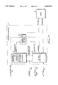
- FIG. 1 is a block diagram of the overall system configuration of the preferred embodiment of the invention.
- FIG. 2 is a more detailed block diagram of a portion of the system shown in FIG. 1;
- FIG. 3 is a more detailed block diagram of another portion of the system shown in FIG. 1;
- FIG. 4 illustrates waveforms useful in explaining the operation of the system shown in FIGS. 1, 2 and 3.
- FIG. 1 illustrates a computer system including a central processing unit (CPU) 12, which is interconnected by address and data multiplex buses 18 and 19 to a system controller 14 and a peripheral controller (COMBO) 16. These components are common in personal computers (PC's), as well as in lap-top and hand-held computer systems.
- CPU central processing unit
- COMBO peripheral controller
- the peripheral controller 16 is interconnected with a single shared system and internal operating system (BIOS) ROM 20 instead of two separate read-only memories (ROM's) for storing the system or keyboard information and the internal operating system information.
- BIOS system and internal operating system
- DRAM direct random access memory
- FIGS. 2 and 3 illustrate in greater detail the internal block diagram configurations of the peripheral controller 16 and the system controller 14, respectively.
- the block diagram circuits, which are illustrated in FIGS. 2 and 3, are directed to the logic interconnections of the peripheral controller 16 and system controller 14, which are utilized to effect the shared ROM operation and signals for the single shared ROM 20, illustrated in FIG. 1 connected to the peripheral controller 16.
- the shared ROM 20 is illustrated in somewhat greater detail in FIG. 2; and the DRAM 22 is shown in FIG. 3 as connected to the system controller through an address bus (MA bus) and a data bus, respectively.
- MA bus address bus
- data bus data bus
- peripheral controller and system controller which are common to PC's and portable and lap-top computers, for the standard operation of these computers, are not shown in FIGS. 1, 2 and 3 to avoid unnecessary cluttering and complexity. Only the shared ROM signal paths and components which are involved in the implementation of the shared ROM operation are illustrated in these figures.
- MRESET--this is the main system reset, which is operated at initial power-up or boot-up of the computer system shown in FIG. 1.
- MLLBA#--this is the multiplex device local bus access signal.
- a multiplex bus device asserts this low, true signal when a valid address transmitted on the CPU address bus is positively decoded. The first occurrence of this signal following the reset of the system at boot is used to latch the system controller 14 for the shared BIOS operation from the ROM 20, immediately following system boot.
- KBDMEM--this is the keyboard register in the configuration register of the system controller 14.
- KROMC--this is the keyboard ROM configuration register in the configuration register set of the peripheral controller 16.
- KRAMM--this is the keyboard RAM bit, which in this system, comprises bit 6 of the KBDMEM register and for the purposes of this system, is always a "0".
- KLCKM--this is a keyboard lock bit comprising bit 5 of the KBDMEM register; and for the purposes of the system shown in FIGS. 1, 2 and 3, this bit is always a "0".
- KROMM#--this is the keyboard ROM memory of the KBDMEM register; and this bit goes to "0" for the shared ROM operation.
- KROMS--this is bit 1 of the KROMC register in the peripheral controller, and is a keyboard ROM shared, which is set by the MRESET signal.
- KBDCTL--this is the keyboard control register.
- KSHRS#--this is bit "0" in the KROMC register, and is always a "0" for operation of the shared ROM system disclosed in FIGS. 1, 2 and 3.
- FIGS. 2 and 3 in conjunction with FIG. 1.
- FIG. 4 indicates the primary control signals which are utilized at the beginning of the system boot to effect the shared ROM operation for utilizing the ROM 20 initially to provide the system BIOS information, and then subsequently to operate as the keyboard subsystem memory.
- a signal MRESET in the form of a positive pulse, is applied to the lead 46 shown in both FIGS. 2 and 3.
- This reset signal is the standard system reset in PC's and functions in its normal manner in the computer system to initialize various circuit components in the configuration registers 30 and 60 of the peripheral controller and system controllers 16 and 14, as well as in the ML bus logic blocks 34 and 64 in each of these controllers.
- this MRESET signal is gated with a ground or binary "0", which is continuously applied on the lead 44 (SHARED#FIG. 2) and through the configuration registers 30 to a shared ROM decode and hit logic 36, to set the peripheral controller 16 to its shared ROM mode of operation.
- the occurrence of the system reset MRESET also operates in the ML bus logic block 64 of the system controller 14 to supply the first multiplex local bus access signal (MLLBA#) over the lead 48 to the configuration register and to the ML bus logic block 34 in the peripheral controller 16.
- MLLBA# first multiplex local bus access signal
- the system controller 14 is configured through the shared ROM decode and hit logic 66 to be configured for its shared ROM BIOS operation.
- the single shared ROM 20 is partitioned or divided into two portions.
- the lower address portion is dedicated to the keyboard microcontroller code information.
- the ROM 20 typically is eight bits wide; and the keyboard information is located in the lower 16K addresses, indicated in FIG. 2 as 0000(Hex) to FFFF(Hex).
- the remainder of the ROM 20, namely the high addresses in the range 8000(Hex) to 3FFFF(Hex) are dedicated to the system BIOS information or CPU code.
- this "high address" portion of the ROM 20 may be 256K. This portion of the ROM may have a capacity greater or smaller than 256K bytes; but in all cases, the BIOS ROM is located in this high address portion of the ROM.
- the peripheral controller 16 operating through the multiplex tree 40 from the shared ROM decode and hit logic 36, in conjunction with the multiplex bus logic block 34 and the keyboard control logic 42, illustrated in FIG. 2.
- the keyboard control is shown as using the Intel® 8051. Other keyboard control logic may be employed; but the specific ports for the address and data coupled between the keyboard controller 42 and the multiplex tree 40 are specific designations for the Intel® 8051.
- Port 0 of the keyboard controller 42 carries address and data (address/data) 7:0, while Port 2 carries address information only for address lines 7:0.
- the combination address/data for line 7:0 is indicated on the lower interconnection between the multiplex tree 40 and the ROM 20 in the address/data lines AD7: ADO interconnecting the multiplex tree 40 and the ROM 20.
- the shared ROM 20 typically is eight bits wide. This is adequate for the 8051 keyboard control system, which is part of the peripheral controller (COMBO); but the system DRAM 22 coupled with the system controller 14 is the same width as the system processor. Typically, this width is thirty-two bits. In order to shadow or transfer the BIOS information from the shared ROM 20 to the DRAM 22, the shared ROM logic must make this translation from eight bits to thirty-two bits. In the system shown in FIGS. 2 and 3, the peripheral controller (COMBO) supplies these eight bits over the data lines D7:D0 from the multiplex tree 40 to the ML bus logic block 34.
- the logic block 34 then converts eight bits to sixteen bit ML bus accesses, which are supplied over the ML bus 50 to the MC bus logic block 64 in the system controller 14. These sixteen bit accesses are translated by the ML bus logic block 64 to the thirty-four bit access for the processor.
- the shared ROM 30 is dedicated to the system BIOS processor; and the keyboard subsystem, operated by the keyboard controller 42, is disabled.
- the logic which responds to the signal waveforms shown in FIG. 4, is conventional gate and latch logic used in the shared ROM decode and hit logic blocks 36 and 66 of the peripheral controller 16 and system controller 14, respectively.
- KBDMEM register In the controller. This controller controls the keyboard ROM/RAM access. It is used to control the downloadable RAM keyboard option, and also has bits for the shared ROM. This register must be updated by software.
- the register is configured as follows:
- bit D6 For the system using the shared ROM 20, bit D6, KRAMM, always is set to "0"; so that the system responds as a shared ROM system.
- bit D5 For the present purposes, this bit always may be considered to be "0".
- Bit D5, KLCKM is a keyboard lock bit; and, again, this bit has no meaning with respect to the operation of the shared ROM circuit of this invention. It is utilized for other functions in the system. Consequently, the only two bits of significance with respect to the shared ROM operation are bits D1 and D0.
- Bit D1, KROMM# is latched at the trailing edge of MRESET to the level on the MLLBA# pin. This is indicated in FIG. 4. If this bit is "0", the shared ROM is enabled; and when the peripheral controller (COMBO) 16 also is set for the shared ROM operation, the system responds as a memory device at the system BIOS range 8000(Hex) to 3FFFF(Hex) indicated on the ROM 20 in FIG. 2. The system controller 14 generates the MLLBA# signals internally in the ML bus logic block 34 for all memory accesses in this range.
- This bit, KROMM# can be set (1) by software, ending the shared ROM mode. This bit cannot be cleared (0) by software, making the shared ROM protected from inadvertent access.
- Bit D0, KSHRM# is latched at the trailing edge of MRESET (low to high transition) to the level on the MLLBA# pin. This bit cannot be changed by software; it is read-only. This bit indicates that a shared ROM was used to boot the system.
- the register KROMC in the COMBO chip has the following configuration:
- Bits 7:5 currently are directed to extended features other than those used for the shared ROM mode.
- the shared ROM mode is enabled independently through the grounded (0) signal (SHARED#) on the lead 44 (FIG. 2).
- Bit D4 of the KROMC register is reserved, and is not used in the shared ROM mode.
- Bits D3:D0 are employed for controlling the address lines and operation of the high addresses for the system BIOS range of the shared ROM 20.
- Bit D1 KROMS is latched at the trailing edge of MRESET, as indicated in FIG. 4, to a value opposite the level on the SHARED# pin (one if SHARED# is low, 0 if SHARED# is high).
- the SHARED# pin always is at "0"; so that the shared ROM is enabled.
- This KROMS bit can be cleared by software, ending the shared ROM mode; but this bit cannot be set by software.
- the shared ROM 20 is protected from inadvertent access.
- Bit D0, KSHRS# is 0 when the SHARED# pin is low. Consequently, a 0 in this bit indicates that the system booted from a shared ROM. This may be used as an indication of the system configuration, even after the shared ROM mode is terminated by the KROMS bit. This bit cannot be changed by software, it is read-only.
- the peripheral controller latches in the state of the SHARED# pin at the trailing edge of MRESET.
- the SHARED# pin is connected to ground, or is a binary "0" in the shared ROM system described herein.
- the ML bus interface in the bus logic block 34 of the peripheral controller 16 responds as a slave device to the boot addresses and the normal BIOS addresses.
- the system controller 14 is responsible for ensuring that ML bus cycles are run for the ROM 20 in the peripheral controller 16.
- the peripheral controller 16 cannot generate the MLLBA# signal because it only connects to the low order address lines, and cannot satisfy the memory timing requirements for the ML bus protocol.
- the address to the shared ROM is shown in FIG. 2 comprising the address on the ML bus (bits A15:A0) and two bits A17:A16 controlled by the KROMC register 31 (Bits D2 and D3 of that register) through the shared ROM decode and hit logic 36.
- RESET is asserted.
- the peripheral controller then asserts MLLBA# low in response to the MRESET, as described above. This provides an indication to the system controller that the shared ROM mode will be used.
- the peripheral controller At the trailing edge of MRESET (high to low transition), the peripheral controller, through the shared ROM decode and hit logic 36, latches in the state of the MLLBA# pin. A low (as shown in FIG. 4) enables the shared ROM feature. A latch (not shown) in the shared ROM decode and hit logic 36 stores this ROM access mode. This latch is only set by MRESET, and cannot be changed by software. As noted above, the bit KSHRM# in the KBDMEM register performs this function.
- the system controller 14 assumes that all memory cycles in the range for the high addresses, namely 8000(Hex) to 3FFFF(Hex) as shown in FIG. 2 for the ROM 20, are for the BIOS ROM.
- the particular 64K ROM segments in this portion of the shared ROM 20 are mapped by the A17:A15 bits to any of four 64K ROM segments.
- the system controller 14 does not use an external MLLBA# pin for the boot process.
- the ROM access mode is set at MRESET time, as described above, to a shared ROM, the system controller 14 generates the MLLBA# internally. It should be noted that internal DRAM hits have a higher priority than the MLLBA#. This allows normal shadow operation to occur.
- the system controller 14 always can assert the internal MLLBA# signal; but the internal signal (as well as the external pin), are ignored when the DRAM controller generates a hit signal. This allows the ROM 20 to be read and the DRAM 22 to be written (later in this sequence).
- the first operating code is fetched from the shared ROM via the ML bus (independent of the level on the MLLBA# pin).
- the system while executing out of the shared ROM 20, addressed at A17:A15 and A14:A8 (see FIG. 2) through the multiplex tree 40, enables and configures the system DRAM 22.
- any portions of the shared ROM 20 which are needed during normal operation of the overall system shown in FIG. 1, are copied to the DRAM 22.
- the top of the shared system BIOS ROM initially exists both at the F000 segment and at the E000 segment.
- the A17 and A16 bits in the KROMC register control the E000 segment window into the 256K shared ROM.
- the E000 window can be used to page one of four 64K banks. As alternate blocks are paged into segment E000, they can be shadowed/moved into the DRAM 22 through the address bus (MA bus) under the control of the shared ROM decode and hit logic 66 supplied with the necessary information through the ML bus logic blocks 34 and 64 and the configuration registers 60.
- MA bus address bus
- the KROMS bit in the peripheral controller configuration register 31 and the KROMM bit in the KBDMEM register 61 in the system controller 14 are switched by software. This disables the shared ROM 20 in preparation for using the shared ROM 20 for exclusive use of the keyboard, under control of the keyboard controller 42 in the peripheral controller 16.
- the keyboard controller 42 operates through the multiplexed low address/data bus lines AD7:AD0 through the multiplex tree 40 to initiate conventional keyboard operation of the ROM 20.
- the ROM address lines A17:A15, which addressed the upper portion of the shared ROM 20 are then set to "0", disabling the BIOS portion of the ROM 20 for the remainder of the operation of the system.
- the keyboard subsystem 38 of the peripheral controller 16 then functions normally. It should be noted that when the shared ROM operation is disabled, the system controller enables the shadow memory for resume functions.
Abstract
Description
__________________________________________________________________________
Data Port
ED    D7
        D6    D5   D4 D3
                        D2 D1    D0
__________________________________________________________________________
KBDMEM  KRAMM KLCKM        KROMM#
                                 KSHRM#
(CAh)
POR Value
      1 0     0    0  0 0  MLLBA#
                                 MLLBA#
__________________________________________________________________________
__________________________________________________________________________
Data Port EDh
        D7
          D6  D5
                D4 D3  D2   D1   D0
__________________________________________________________________________
KROMC   EXFEA   R  KA17
                       KA16 KROMS
                                 KSHRS#
Index 5Eh
POR Value
        0 0   0 0  1   1    SHARE
                                 SHAREN
                            N#pin
                                 #pin
__________________________________________________________________________
Claims (5)
Priority Applications (1)
| Application Number | Priority Date | Filing Date | Title |
|---|---|---|---|
| US08/188,373 US5603055A (en) | 1994-01-27 | 1994-01-27 | Single shared ROM for storing keyboard microcontroller code portion and CPU code portion and disabling access to a portion while accessing to the other |
Applications Claiming Priority (1)
| Application Number | Priority Date | Filing Date | Title |
|---|---|---|---|
| US08/188,373 US5603055A (en) | 1994-01-27 | 1994-01-27 | Single shared ROM for storing keyboard microcontroller code portion and CPU code portion and disabling access to a portion while accessing to the other |
Publications (1)
| Publication Number | Publication Date |
|---|---|
| US5603055A true US5603055A (en) | 1997-02-11 |
Family
ID=22692865
Family Applications (1)
| Application Number | Title | Priority Date | Filing Date |
|---|---|---|---|
| US08/188,373 Expired - Lifetime US5603055A (en) | 1994-01-27 | 1994-01-27 | Single shared ROM for storing keyboard microcontroller code portion and CPU code portion and disabling access to a portion while accessing to the other |
Country Status (1)
| Country | Link |
|---|---|
| US (1) | US5603055A (en) |
Cited By (19)
| Publication number | Priority date | Publication date | Assignee | Title |
|---|---|---|---|---|
| US5696968A (en) * | 1995-09-21 | 1997-12-09 | Dell U.S.A., L.P. | Method and apparatus for effecting drive ordering via adapter preference |
| US5794054A (en) * | 1996-07-19 | 1998-08-11 | Compaq Computer Corporation | Flash ROM sharing between a processor and a controller |
| US5805882A (en) * | 1996-07-19 | 1998-09-08 | Compaq Computer Corporation | Computer system and method for replacing obsolete or corrupt boot code contained within reprogrammable memory with new boot code supplied from an external source through a data port |
| US5819087A (en) * | 1996-07-19 | 1998-10-06 | Compaq Computer Corporation | Flash ROM sharing between processor and microcontroller during booting and handling warm-booting events |
| US5892943A (en) * | 1996-12-30 | 1999-04-06 | Standard Microsystems Corp. | Shared bios ROM warm boot |
| US6032254A (en) * | 1996-04-26 | 2000-02-29 | Oki Electric Industry Co., Ltd. | Method of identifying peripheral device employed in a semiconductor device |
| US6148373A (en) * | 1997-05-29 | 2000-11-14 | United Microelectronics Corp. | Apparatus and methods for increasing memory utilization |
| US6240519B1 (en) | 1998-04-30 | 2001-05-29 | Compaq Computer Corporation | Computer method and apparatus to prompt for administrative password to flash a corrupted non-volatile memory |
| US6286097B1 (en) * | 1998-08-06 | 2001-09-04 | Via Technologies, Inc. | Computer chipset for accessing a conventional read only memory (ROM) |
| US6363492B1 (en) | 1998-04-30 | 2002-03-26 | Compaq Computer Corporation | Computer method and apparatus to force boot block recovery |
| US6446139B1 (en) * | 1999-06-28 | 2002-09-03 | Adaptec, Inc. | Multiple chip single image BIOS |
| US6490357B1 (en) * | 1998-08-28 | 2002-12-03 | Qualcomm Incorporated | Method and apparatus for generating encryption stream ciphers |
| US20030061603A1 (en) * | 2001-09-21 | 2003-03-27 | Chih-Chien Tang | Method and device for updating keyboard controller BIOS through serial port |
| US20070208929A1 (en) * | 2006-03-02 | 2007-09-06 | Via Technologies, Inc. | Device information managements systems and methods |
| EP1840754A2 (en) * | 2006-03-30 | 2007-10-03 | Pioneer Corporation | Information processing device |
| US20090043916A1 (en) * | 2007-08-06 | 2009-02-12 | Winbond Electronics Corporation | Handshake Free Sharing in a Computer Architecture |
| US20100241838A1 (en) * | 2009-03-20 | 2010-09-23 | Jason Cohen | Method and system for firmware updates |
| WO2010132189A1 (en) * | 2009-05-15 | 2010-11-18 | Thomson Licensing | System and method for sharing memory |
| US20160103784A1 (en) * | 2014-10-08 | 2016-04-14 | Cognivue Corporation | Asymmetrical processor memory architecture |
Citations (10)
| Publication number | Priority date | Publication date | Assignee | Title |
|---|---|---|---|---|
| US4028675A (en) * | 1973-05-14 | 1977-06-07 | Hewlett-Packard Company | Method and apparatus for refreshing semiconductor memories in multi-port and multi-module memory system |
| US4713759A (en) * | 1984-01-27 | 1987-12-15 | Mitsubishi Denki Kabushiki Kaisha | Memory bank switching apparatus |
| JPS6474646A (en) * | 1987-09-16 | 1989-03-20 | Ricoh Kk | Read-only memory and controller using same memory |
| US4908789A (en) * | 1987-04-01 | 1990-03-13 | International Business Machines Corporation | Method and system for automatically assigning memory modules of different predetermined capacities to contiguous segments of a linear address range |
| US4926372A (en) * | 1986-05-06 | 1990-05-15 | Nintendo Company Limited | Memory cartridge bank selecting |
| JPH0461578A (en) * | 1990-06-29 | 1992-02-27 | Nec Home Electron Ltd | Video printer |
| US5101490A (en) * | 1989-01-10 | 1992-03-31 | Bull Hn Information Systems Inc. | Peripheral device controller with an EEPROM with microinstructions for a RAM control store |
| US5109521A (en) * | 1986-09-08 | 1992-04-28 | Compaq Computer Corporation | System for relocating dynamic memory address space having received microprocessor program steps from non-volatile memory to address space of non-volatile memory |
| US5287481A (en) * | 1991-12-19 | 1994-02-15 | Opti, Inc. | Automatic cache flush with readable and writable cache tag memory |
| US5473775A (en) * | 1991-10-11 | 1995-12-05 | Kabushiki Kaisha Toshiba | Personal computer using flash memory as BIOS-ROM |
-
1994
- 1994-01-27 US US08/188,373 patent/US5603055A/en not_active Expired - Lifetime
Patent Citations (11)
| Publication number | Priority date | Publication date | Assignee | Title |
|---|---|---|---|---|
| US4028675A (en) * | 1973-05-14 | 1977-06-07 | Hewlett-Packard Company | Method and apparatus for refreshing semiconductor memories in multi-port and multi-module memory system |
| US4713759A (en) * | 1984-01-27 | 1987-12-15 | Mitsubishi Denki Kabushiki Kaisha | Memory bank switching apparatus |
| US4926372A (en) * | 1986-05-06 | 1990-05-15 | Nintendo Company Limited | Memory cartridge bank selecting |
| US5109521A (en) * | 1986-09-08 | 1992-04-28 | Compaq Computer Corporation | System for relocating dynamic memory address space having received microprocessor program steps from non-volatile memory to address space of non-volatile memory |
| US4908789A (en) * | 1987-04-01 | 1990-03-13 | International Business Machines Corporation | Method and system for automatically assigning memory modules of different predetermined capacities to contiguous segments of a linear address range |
| JPS6474646A (en) * | 1987-09-16 | 1989-03-20 | Ricoh Kk | Read-only memory and controller using same memory |
| US5101490A (en) * | 1989-01-10 | 1992-03-31 | Bull Hn Information Systems Inc. | Peripheral device controller with an EEPROM with microinstructions for a RAM control store |
| JPH0461578A (en) * | 1990-06-29 | 1992-02-27 | Nec Home Electron Ltd | Video printer |
| US5473775A (en) * | 1991-10-11 | 1995-12-05 | Kabushiki Kaisha Toshiba | Personal computer using flash memory as BIOS-ROM |
| US5287481A (en) * | 1991-12-19 | 1994-02-15 | Opti, Inc. | Automatic cache flush with readable and writable cache tag memory |
| US5423019A (en) * | 1991-12-19 | 1995-06-06 | Opti Inc. | Automatic cache flush with readable and writable cache tag memory |
Cited By (24)
| Publication number | Priority date | Publication date | Assignee | Title |
|---|---|---|---|---|
| US5696968A (en) * | 1995-09-21 | 1997-12-09 | Dell U.S.A., L.P. | Method and apparatus for effecting drive ordering via adapter preference |
| US6032254A (en) * | 1996-04-26 | 2000-02-29 | Oki Electric Industry Co., Ltd. | Method of identifying peripheral device employed in a semiconductor device |
| US5794054A (en) * | 1996-07-19 | 1998-08-11 | Compaq Computer Corporation | Flash ROM sharing between a processor and a controller |
| US5805882A (en) * | 1996-07-19 | 1998-09-08 | Compaq Computer Corporation | Computer system and method for replacing obsolete or corrupt boot code contained within reprogrammable memory with new boot code supplied from an external source through a data port |
| US5819087A (en) * | 1996-07-19 | 1998-10-06 | Compaq Computer Corporation | Flash ROM sharing between processor and microcontroller during booting and handling warm-booting events |
| US6154838A (en) * | 1996-07-19 | 2000-11-28 | Le; Hung Q. | Flash ROM sharing between processor and microcontroller during booting and handling warm-booting events |
| US5892943A (en) * | 1996-12-30 | 1999-04-06 | Standard Microsystems Corp. | Shared bios ROM warm boot |
| US6148373A (en) * | 1997-05-29 | 2000-11-14 | United Microelectronics Corp. | Apparatus and methods for increasing memory utilization |
| US6240519B1 (en) | 1998-04-30 | 2001-05-29 | Compaq Computer Corporation | Computer method and apparatus to prompt for administrative password to flash a corrupted non-volatile memory |
| US6363492B1 (en) | 1998-04-30 | 2002-03-26 | Compaq Computer Corporation | Computer method and apparatus to force boot block recovery |
| US6286097B1 (en) * | 1998-08-06 | 2001-09-04 | Via Technologies, Inc. | Computer chipset for accessing a conventional read only memory (ROM) |
| US6490357B1 (en) * | 1998-08-28 | 2002-12-03 | Qualcomm Incorporated | Method and apparatus for generating encryption stream ciphers |
| US6446139B1 (en) * | 1999-06-28 | 2002-09-03 | Adaptec, Inc. | Multiple chip single image BIOS |
| US20030061603A1 (en) * | 2001-09-21 | 2003-03-27 | Chih-Chien Tang | Method and device for updating keyboard controller BIOS through serial port |
| US20070208929A1 (en) * | 2006-03-02 | 2007-09-06 | Via Technologies, Inc. | Device information managements systems and methods |
| EP1840754A2 (en) * | 2006-03-30 | 2007-10-03 | Pioneer Corporation | Information processing device |
| US20070288722A1 (en) * | 2006-03-30 | 2007-12-13 | Pioneer Corporation | Information processing device |
| EP1840754A3 (en) * | 2006-03-30 | 2009-07-08 | Pioneer Corporation | Information processing device |
| US20090043916A1 (en) * | 2007-08-06 | 2009-02-12 | Winbond Electronics Corporation | Handshake Free Sharing in a Computer Architecture |
| US8285895B2 (en) | 2007-08-06 | 2012-10-09 | Winbond Electronics Corporation | Handshake free sharing in a computer architecture |
| US20100241838A1 (en) * | 2009-03-20 | 2010-09-23 | Jason Cohen | Method and system for firmware updates |
| WO2010132189A1 (en) * | 2009-05-15 | 2010-11-18 | Thomson Licensing | System and method for sharing memory |
| US20160103784A1 (en) * | 2014-10-08 | 2016-04-14 | Cognivue Corporation | Asymmetrical processor memory architecture |
| US11656874B2 (en) * | 2014-10-08 | 2023-05-23 | Nxp Usa, Inc. | Asymmetrical processor memory architecture |
Similar Documents
| Publication | Publication Date | Title |
|---|---|---|
| US5603055A (en) | Single shared ROM for storing keyboard microcontroller code portion and CPU code portion and disabling access to a portion while accessing to the other | |
| US5659748A (en) | Booting of multiprocessor system from a boot ROM of narrower width than the system memory | |
| JP2633458B2 (en) | DMA channel device and DMA channel conversion device | |
| US5608876A (en) | Add-in board with enable-disable expansion ROM for PCI bus computers | |
| JP2571673B2 (en) | Method and apparatus for providing back-to-back data transfer in an information processing system having a multiplexed bus | |
| US5734847A (en) | Method and apparatus for enabling intelligent I/O subsystems using PCI I/O devices | |
| US5155833A (en) | Multi-purpose cache memory selectively addressable either as a boot memory or as a cache memory | |
| US5848249A (en) | Method and apparatus for enabling intelligent I/O subsystems using PCI I/O devices | |
| US5911084A (en) | System and method for accessing peripheral devices on a non-functional controller | |
| EP0780772A2 (en) | A computer system with multiple PC card controllers and a method of controlling I/O transfers in the system | |
| US5515514A (en) | Peripheral processor card for upgrading a computer | |
| US5550989A (en) | Bridge circuit that can eliminate invalid data during information transfer between buses of different bitwidths | |
| US20010018721A1 (en) | Upgrade card for a computer system | |
| US5922062A (en) | Combined IDE and SCSI disk controller interface for common hardware reference platforms | |
| US6636904B2 (en) | Dynamic PCI device identification redirection on a configuration space access conflict | |
| WO1993000640A1 (en) | Method and apparatus for expanding a backplane interconnecting bus without additional byte select signals | |
| US5887157A (en) | Local bus interface | |
| US5577214A (en) | Programmable hold delay | |
| US7058779B1 (en) | Computer system initialization via boot code stored in a non-volatile memory having an interface compatible with synchronous dynamic random access memory | |
| US5860113A (en) | System for using a dirty bit with a cache memory | |
| US6457137B1 (en) | Method for configuring clock ratios in a microprocessor | |
| US20040098516A1 (en) | Booting from a re-programmable memory on an unconfigured bus | |
| US5600802A (en) | Methods and apparatus for translating incompatible bus transactions | |
| US5961643A (en) | Method for attachment or integration of a BIOS device into a computer system using the system memory address and data bus | |
| US5477503A (en) | Efficient local-bus ROM memory for microprocessor systems |
Legal Events
| Date | Code | Title | Description |
|---|---|---|---|
| AS | Assignment |
Owner name: VLSI TECHNOLOGY, INC, CALIFORNIA Free format text: ASSIGNMENT OF ASSIGNORS INTEREST;ASSIGNORS:EVOY, DAVID R.;GOULD, LAWRENCE D.;EDWARDS, JAMES R.;AND OTHERS;REEL/FRAME:006947/0489;SIGNING DATES FROM 19940329 TO 19940331 |
|
| STCF | Information on status: patent grant |
Free format text: PATENTED CASE |
|
| FEPP | Fee payment procedure |
Free format text: PAYOR NUMBER ASSIGNED (ORIGINAL EVENT CODE: ASPN); ENTITY STATUS OF PATENT OWNER: LARGE ENTITY |
|
| FPAY | Fee payment |
Year of fee payment: 4 |
|
| FPAY | Fee payment |
Year of fee payment: 8 |
|
| AS | Assignment |
Owner name: PHILIPS SEMICONDUCTORS VLSI INC., NEW YORK Free format text: CHANGE OF NAME;ASSIGNOR:VLSI TECHNOLOGY, INC.;REEL/FRAME:018635/0570 Effective date: 19990702 Owner name: NXP B.V., NETHERLANDS Free format text: ASSIGNMENT OF ASSIGNORS INTEREST;ASSIGNOR:PHILIPS SEMICONDUCTORS INC.;REEL/FRAME:018645/0779 Effective date: 20061130 |
|
| AS | Assignment |
Owner name: PHILIPS SEMICONDUCTORS INC., NEW YORK Free format text: CHANGE OF NAME;ASSIGNOR:PHILIPS SEMICONDUCTORS VLSI INC.;REEL/FRAME:018668/0255 Effective date: 19991220 |
|
| FPAY | Fee payment |
Year of fee payment: 12 |
|
| REMI | Maintenance fee reminder mailed |