US5599740A - Deposit-etch-deposit ozone/teos insulator layer method - Google Patents
Deposit-etch-deposit ozone/teos insulator layer method Download PDFInfo
- Publication number
- US5599740A US5599740A US08/558,491 US55849195A US5599740A US 5599740 A US5599740 A US 5599740A US 55849195 A US55849195 A US 55849195A US 5599740 A US5599740 A US 5599740A
- Authority
- US
- United States
- Prior art keywords
- layer
- silicon oxide
- oxide insulator
- patterned
- layers
- Prior art date
- Legal status (The legal status is an assumption and is not a legal conclusion. Google has not performed a legal analysis and makes no representation as to the accuracy of the status listed.)
- Expired - Lifetime
Links
Images


Classifications
-
- H—ELECTRICITY
- H01—ELECTRIC ELEMENTS
- H01L—SEMICONDUCTOR DEVICES NOT COVERED BY CLASS H10
- H01L21/00—Processes or apparatus adapted for the manufacture or treatment of semiconductor or solid state devices or of parts thereof
- H01L21/02—Manufacture or treatment of semiconductor devices or of parts thereof
- H01L21/04—Manufacture or treatment of semiconductor devices or of parts thereof the devices having at least one potential-jump barrier or surface barrier, e.g. PN junction, depletion layer or carrier concentration layer
- H01L21/18—Manufacture or treatment of semiconductor devices or of parts thereof the devices having at least one potential-jump barrier or surface barrier, e.g. PN junction, depletion layer or carrier concentration layer the devices having semiconductor bodies comprising elements of Group IV of the Periodic System or AIIIBV compounds with or without impurities, e.g. doping materials
- H01L21/30—Treatment of semiconductor bodies using processes or apparatus not provided for in groups H01L21/20 - H01L21/26
- H01L21/31—Treatment of semiconductor bodies using processes or apparatus not provided for in groups H01L21/20 - H01L21/26 to form insulating layers thereon, e.g. for masking or by using photolithographic techniques; After treatment of these layers; Selection of materials for these layers
- H01L21/3105—After-treatment
- H01L21/31051—Planarisation of the insulating layers
- H01L21/31053—Planarisation of the insulating layers involving a dielectric removal step
-
- H—ELECTRICITY
- H01—ELECTRIC ELEMENTS
- H01L—SEMICONDUCTOR DEVICES NOT COVERED BY CLASS H10
- H01L21/00—Processes or apparatus adapted for the manufacture or treatment of semiconductor or solid state devices or of parts thereof
- H01L21/70—Manufacture or treatment of devices consisting of a plurality of solid state components formed in or on a common substrate or of parts thereof; Manufacture of integrated circuit devices or of parts thereof
- H01L21/71—Manufacture of specific parts of devices defined in group H01L21/70
- H01L21/768—Applying interconnections to be used for carrying current between separate components within a device comprising conductors and dielectrics
- H01L21/76801—Applying interconnections to be used for carrying current between separate components within a device comprising conductors and dielectrics characterised by the formation and the after-treatment of the dielectrics, e.g. smoothing
- H01L21/76837—Filling up the space between adjacent conductive structures; Gap-filling properties of dielectrics
Definitions
- the present invention relates generally to insulator layers formed within integrated circuits. More particularly, the present invention relates to gap filling and self-planarizing silicon oxide insulator spacer layers selectively formed within patterned layers within integrated circuits.
- Integrated circuits are typically fabricated from semiconductor substrates upon whose surfaces are formed a multiplicity of active semiconductor regions. Within those active semiconductor regions are formed transistors, resistors, diodes and other electrical circuit elements. Those electrical circuit elements are interconnected internally and externally to the semiconductor substrates upon which they are formed through the use of patterned conductor metal layers which are separated by insulator layers.
- patterned conductor metal layer line-widths and spacings within advanced semiconductor integrated circuits have continued to decrease while aspect ratios of those patterned conductor metal lines have continued to increase.
- Yu in U.S Pat. No. 5,302,555 discloses a method for preferentially depositing a silicon oxide coating on horizontal surfaces of structured semiconductor substrates.
- the method involves control of several parameters related to the gaseous reactant mixture from which is deposited the silicon oxide coating and several additional parameters related to design of the reactor within which is deposited the silicon oxide coating.
- Significant parameters which are controlled include the flow ratio of reactant gases, the reactor pressure and the geometry of the susceptor within the reactor.
- Hieber discloses a method for locally and globally planarizing a structured semiconductor substrate with a silicon oxide layer formed through an ozone activated Chemical Vapor Deposition (CVD) process.
- the method employs a structured semiconductor substrate fabricated from materials at the lower levels of the structure which have inherently increased growth rates for silicon oxide layers formed through an ozone activated Chemical Vapor Deposition (CVD) process.
- the method preferably employs a Boro Phospho Silicate Glass (BPSG) or a Phospho Silicate Glass (PSG) lower layer.
- the method also employs a Plasma Enhanced Chemical Vapor Deposited (PECVD) silicon oxide upper layer to retard growth upon metallization layers which otherwise typically form upper layers of the structured semiconductor substrate.
- PECVD Plasma Enhanced Chemical Vapor Deposited
- Desirable in the art are methods and materials which expand from the Hiebert disclosure and yield silicon oxide insulator spacer layers which have excellent gap filling and self-planarizing properties. Most desirable are gap filling and self-planarizing silicon oxide insulator spacer layers which may be formed selectively between adjoining structures of a patterned layer, such as a patterned metal layer, within an advanced integrated circuit, but not upon the top surfaces of those adjoining structures.
- a first object of the present invention is to provide a gap filling and self-planarizing silicon oxide insulator spacer layer selectively deposited between adjoining structures of a patterned layer within an integrated circuit, such as the adjoining structures of a patterned metal layer within an integrated circuit, but not on the surfaces of those adjoining structures.
- a second object of the present invention is to provide a gap filling and self-planarizing silicon oxide insulator spacer layer in accord with the first object of the present invention, which silicon oxide insulator spacer layer is readily manufacturable.
- a third object of the present invention is to provide a gap filling and self-planarizing silicon oxide insulator spacer layer in accord with the first object of the present invention and the second object of the present invention, which silicon oxide insulator spacer layer is economical.
- a method for forming a gap filling and self-planarizing silicon oxide insulator spacer layer is disclosed.
- the patterned integrated circuit layer is structured with an upper-most layer formed of titanium nitride and at least one lower-lying layer formed of a material having a more rapid growth rate with respect to ozone assisted Chemical Vapor Deposited (CVD) silicon oxide insulator layers than titanium nitride.
- CVD Chemical Vapor Deposited
- a silicon oxide insulator spacer layer deposited through an ozone assisted Chemical Vapor Deposition (CVD) process.
- the silicon oxide insulator spacer layer is formed until the surface of the titanium nitride upper-most layer is passivated with the silicon oxide insulator spacer layer.
- the silicon oxide insulator spacer layer is etched from the surface of the titanium nitride upper-most layer.
- the preceding silicon oxide insulator spacer layer deposition and etching processes are sequentially repeated until the surface of the silicon oxide insulator spacer layer over the lower-lying layer(s) of the patterned integrated circuit layer is planar with the upper surface of the titanium nitride upper-most layer.
- the gap filling and self-planarizing silicon oxide insulator spacer layer of the present invention is selectively deposited between adjoining structures of a patterned layer within an integrated circuit, such as the adjoining structures of a patterned metal layer within an integrated circuit, but not on the surfaces of those adjoining structures.
- the patterned layer into which the silicon oxide insulator spacer layer of the present invention is formed from a titanium nitride upper-most layer which has a slower growth rate with respect to ozone assisted Chemical Vapor Deposited (CVD) silicon oxide layers than materials from which are formed lower-lying layers of the patterned integrated circuit layer, it is possible to efficiently fill and planarize the gaps within the patterned integrated circuit layer while providing minimal silicon oxide insulator spacer layer build-up on the upper-most layers of the patterned integrated circuit layer.
- CVD Chemical Vapor Deposited
- the present invention provides a silicon oxide insulator spacer layer selectively deposited within a patterned integrated circuit layer, but not upon the surfaces of those structures which form the patterns of the patterned integrated circuit layer.
- the method of the present invention provides a silicon oxide insulator spacer layer which is readily manufacturable.
- the method of the present invention employs successive deposition and etch cycles to provide a gap filling and self-planarizing silicon oxide insulator spacer layer formed within a patterned integrated circuit layer where upper-most layers of the structures of the patterned integrated circuit layer have less rapid growth rates with respect to ozone assisted Chemical Vapor Deposited (CVD) silicon oxide insulator layers than lower-lying layers of the structures of the patterned integrated circuit layer.
- CVD Chemical Vapor Deposited
- the sequential and repeated deposition and etching processes of the present invention, as well as the materials from which are formed the upper-most layers and the lower-lying layers of the patterned integrated circuit layers within which is formed the silicon oxide insulator spacer layer of the present invention, are known in the art. Since no new manufacturing equipment, manufacturing processes or materials are needed in forming the silicon oxide insulator spacer layer of the present invention, the method by which is formed the silicon oxide insulator spacer layer of the present invention is manufacturable. For analogous reasons, the silicon oxide insulator spacer layer of the present invention is also economical.
- FIG. 1a to FIG. 1g illustrate progressive stages in forming an integrated circuit comprising the preferred embodiment of the present invention, into which integrated circuit are formed silicon oxide insulator spacer layers of the present invention.
- FIG. 2 shows a graph of Insulator Spacer Layer Thickness vs. Deposition Time for forming the silicon oxide insulator spacer layers of the present invention upon the substrate layers of the preferred embodiment of the present invention.
- the present invention provides a method for forming a gap filling and self-planarizing silicon oxide insulator spacer layer within, but not upon, integrated circuit structures which form patterned integrated circuit layers.
- the present invention provides a silicon oxide insulator spacer layer which is formed preferentially upon lower-lying layers of an integrated circuit structure within a patterned integrated circuit and not upon the surfaces of upper-most lying layers of that structure.
- the viability of the method of the present invention derives from the substantial differences in growth rates that have been observed for ozone assisted Chemical Vapor Deposited (CVD) silicon oxide layers formed upon different substrate materials. These growth rate differences have been described in detail in other disclosures from this laboratory. For example, see S. M. Jang et al., "Method for Selectively Depositing Silicon Oxide Spacer Layers," U.S. patent application Ser. No. 08/518,706 filed Aug. 24, 1995, U.S. Pat. No. 5,518,959.
- the gap filling and self-planarizing silicon oxide insulator layer of the present invention By forming the structures of the patterned integrated circuit layers within which the gap filling and self-planarizing silicon oxide insulator layer of the present invention is deposited from lower-lying layers having a high growth rate for ozone assisted Chemical Vapor Deposited (CVD) silicon oxide layers and upper-most lying layers having a low growth rate for ozone assisted Chemical Vapor Deposited (CVD) silicon oxide layers, there may be formed the gap filling and self-planarizing silicon oxide insulator spacer layer of the present invention which is formed more rapidly between the structures of a patterned integrated circuit layer than upon the surfaces of those structures.
- CVD chemical Vapor Deposited
- the gap filling and self-planarizing silicon oxide insulator spacer layer of the present invention through multiple deposition process steps separated by multiple intervening etch process steps, the thin gap filling and self-planarizing silicon oxide insulator spacer layer of the present invention which is formed upon the surface of a titanium nitride upper-most layer of the patterned integrated circuit layer structure may be removed.
- the gap filling and self-planarizing silicon oxide insulator spacer layer of the present invention there is formed the gap filling and self-planarizing silicon oxide insulator spacer layer of the present invention.
- the gap filling and self planarizing silicon oxide insulator spacer layer of the present invention may be formed within any integrated circuit wherein there is needed a gap filling and self-planarizing silicon oxide insulator spacer layer which is selectively formed between, but not upon, structures within patterned integrated circuit layers.
- a gap filling and self-planarizing silicon oxide insulator spacer layer of the present invention will be formed within the structures of a patterned metal layer within an integrated circuit.
- the gap filling and self planarizing silicon oxide insulator spacer layer of the present invention may be used as a silicon oxide insulator spacer layer within a first patterned metal layer within an integrated circuit, within a second patterned metal layer within an integrated circuit or within any subsequent patterned metal layer(s) within an integrated circuit.
- the gap filling and self-planarizing silicon oxide insulator spacer layer of the present invention also has broad applicability as a silicon oxide insulator spacer layer within various types of integrated circuits.
- the gap filling and self-planarizing silicon oxide insulator spacer layer of the present invention may be used in integrated circuits including but not limited to Dynamic Random Access Memory (DRAM) integrated circuits, Static Random Access Memory (SRAM) integrated circuits, Application Specific Integrated Circuits (ASICs), integrated circuits having field effect transistors formed within their structures and integrated circuits having bipolar transistors formed within their structures.
- DRAM Dynamic Random Access Memory
- SRAM Static Random Access Memory
- ASICs Application Specific Integrated Circuits
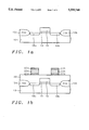
- FIG. 1a to FIG. 1g there is shown a series of schematic cross-sectional diagrams illustrating progressive stages in forming an integrated circuit which provides the preferred embodiment into which the silicon oxide insulator spacer layer of the present invention is formed. Shown in FIG. 1a is the integrated circuit at the early stages of fabrication.
- FIG. 1a shows a semiconductor substrate 10 upon and within whose surface there are formed isolation regions 12a and 12b.
- Semiconductor substrates upon which the present invention may be practiced may be formed with either dopant polarity, any dopant concentration and any crystallographic orientation.
- the semiconductor substrate 10 upon which is practiced the present invention will be a N- or P-silicon semiconductor substrate having a (100) crystallographic orientation.
- isolation regions may be formed within and upon semiconductor substrates. Such methods include but are not limited to methods whereby a portion of a semiconductor substrate exposed through an appropriate mask is oxidized to form isolation regions within and upon the semiconductor substrate, and methods whereby a separate insulating layer is formed upon a semiconductor substrate surface and subsequently patterned to form isolation regions upon the semiconductor substrate.
- the isolation regions 12a and 12b are preferably formed through a thermal oxidation process whereby portions of the semiconductor substrate 10 exposed through an oxidation mask are consumed to form within and upon the semiconductor substrate 10 isolation regions 12a and 12b of silicon oxide.
- a gate oxide 14 upon which resides a gate electrode 16. Both the gate oxide 14 and the gate electrode 16 reside upon the active semiconductor region of the semiconductor substrate 10. Both the gate oxide 14 and the gate electrode 16 are components of a field effect transistor.
- Gate oxides may be formed through methods including but not limited to methods whereby the surface of the active semiconductor region of a semiconductor substrate is oxidized to form a blanket gate oxide layer upon the active semiconductor region, and methods whereby a blanket gate oxide layer is independently deposited upon the surface of the active semiconductor region. Excess portions of blanket gate oxide layers formed upon active semiconductor regions may be removed through etching processes conventional to the art.
- Gate electrodes are typically formed via patterning and etching through methods as are conventional in the art of blanket layers of gate electrode materials which are formed upon the surfaces of blanket gate oxide layers.
- blanket layers of gate electrode materials are formed from highly conductive materials such as metals, metal alloys, highly doped polysilicon and polycides (polysilicon/metal silicide stacks).
- the gate oxide 14 is preferably formed through patterning of a blanket gate oxide layer formed through thermal oxidation of the active semiconductor region of semiconductor substrate 10 at a temperature of about 800 to about 1000 degrees centigrade to yield a typical blanket gate oxide layer thickness of about 80 to about 140 angstroms.
- the gate electrode 16 is preferably formed by patterning and etching a blanket layer of highly doped polysilicon formed upon the blanket gate oxide layer at a thickness of about 2500 to about 3000 angstroms through a Chemical Vapor Deposition (CVD) process employing silane as the silicon source material, along with suitable dopant species.
- CVD Chemical Vapor Deposition
- the gate electrode may be used as an etch mask to pattern the gate oxide 14 from the blanket gate oxide layer.
- source/drain electrodes 18a and 18b formed within the surface of the active semiconductor region of the semiconductor substrate 10 at areas not occupied by the gate electrode 16, the gate oxide 14 and the isolation regions 12a and 12b.
- Methods and materials through which source/drain electrodes may be formed within semiconductor substrates are known in the art. Such methods typically employ dopant species which are ionized and implanted into a semiconductor substrate at sufficient velocity and dose to form into the semiconductor substrate a region of conductivity sufficient for a source/drain electrode. The polarity desired for the source/drain electrode will dictate the polarity of the dopant species. Arsenic dopant species, boron dopant species and phosphorus dopant species are common in the art.
- the source/drain electrodes 18a and 18b are preferably formed through implanting a suitable dopant species into the active region of the semiconductor substrate 10 at about 4 E13 to about 7 E13 ions per square centimeter dose and about 100 to about 130 keV ion implantation energy.
- FIG. 1b Shown in FIG. 1b is the presence of a planarized first silicon oxide insulator substrate layer 20 formed upon the semiconductor substrate 10 illustrated in FIG. 1a.
- a planarized first silicon oxide insulator substrate layer 20 Formed upon the planarized first silicon oxide insulator substrate layer 20 is a pair of three-layer patterned first metal stacks. Within the pair of three-layer patterned first metal stacks, there resides at the bottoms a pair of patterned first lower barrier metal layers 21a and 21b.
- Upon the patterned first lower barrier metal layers 21a and 21b resides a pair of patterned first conductor metal layers 22a and 22b, and upon the pair of patterned first conductor metal layers 22a and 22b resides a pair of patterned first upper barrier metal layers 23a and 23b.
- each of the component layers shown within FIG. 1b is important to the present invention.
- the viability of the preferred embodiment of the present invention derives from differences in growth rates of silicon oxide insulator spacer layers formed through ozone assisted Chemical Vapor Deposition (CVD) processes upon: (1) silicon oxide insulator substrate layers, (2) aluminum containing alloy conductor metal layers, and (3) titanium nitride barrier metal layers formed upon aluminum containing alloy conductor metal layers.
- CVD Chemical Vapor Deposition
- the ratio of the growth rate of a silicon oxide insulator spacer layer formed through an ozone assisted Chemical Vapor Deposition (CVD) process upon a titanium nitride upper-most metal layer within a patterned integrated circuit with respect to the growth rate of that same silicon oxide insulator spacer layer upon an under-lying silicon oxide insulator substrate layer or aluminum containing alloy conductor metal layer within the same integrated circuit is no greater than about 1:2.
- the depth of the integrated circuit pattern into which is formed the gap filling and self-planarizing silicon oxide insulator spacer layer of the present invention is from about 5000 to about 10000 angstroms.
- the planarized first silicon oxide insulator substrate layer 20 is formed through planarizing a conformal first silicon oxide insulator substrate layer which is formed through a Plasma Enhanced Chemical Vapor Deposition (PECVD) process.
- PECVD Plasma Enhanced Chemical Vapor Deposition
- Processes through which a conformal first silicon oxide insulator substrate layer may be planarized are known in the art. Typically, such process involve Reactive Ion Etch (RIE) planarizing or Chemical-Mechanical Polish (CMP) planarizing.
- RIE Reactive Ion Etch
- CMP Chemical-Mechanical Polish
- the Plasma Enhanced Chemical Vapor Deposition (PECVD) processes through which may be formed the planarized first silicon oxide insulator substrate layer 20 are known in the art to form dense and impervious conformal silicon oxide insulator substrate layers.
- silicon source materials may be employed in forming the conformal first silicon oxide insulator substrate layer from which is formed the planarized first silicon oxide insulator substrate layer 20.
- silicon source materials include but are not limited to Tetra Ethyl Ortho Silicate (TEOS), silane, Octa Methyl Cyclo Tetra Siloxane (OMCTS) and Hexa Methyl Di-Silazane (HMDS).
- TEOS Tetra Ethyl Ortho Silicate
- silane silane
- OMCTS Octa Methyl Cyclo Tetra Siloxane
- HMDS Hexa Methyl Di-Silazane
- the preferred materials from which the planarized first silicon oxide insulator substrate layer 20 is formed are silane and Tetra Ethyl Ortho Silicate
- the next important elements to the present invention are the materials from which are formed the pair of patterned first conductor metal layers 22a and 22b, and the pair of patterned first upper barrier metal layers 23a and 23b. It is important to the present invention that the patterned first conductor metal layers 22a and 22b are formed from an aluminum containing alloy. Preferably the patterned first conductor metal layers 22a and 22b are formed of an aluminum containing alloy containing about 0.5 to about 1.0 percent copper. Preferably, the patterned first conductor metal layers 22a and 22b are formed at about 4000 to about 6000 angstroms thickness.
- the pair of patterned first upper barrier metal layers 23a and 23b are formed of titanium nitride, preferably at a thickness of about 1000 to about 1400 angstroms.
- the pair of patterned first lower barrier metal layers 21a and 21b are also preferably formed from titanium nitride, preferably at a thickness of about 800 to about 1200 angstroms.
- the total thickness of the three-layer patterned first metal stacks within which is selectively formed the gap filling and self-planarizing silicon oxide insulator spacer layer of the present invention are about 5800 to about 8600 angstroms each.
- Methods through which the patterned first lower barrier metal layers 21a and 21b, the patterned first conductor metal layers 22a and 22b and the patterned first upper barrier metal layers 23a and 23b may be formed upon the planarized first silicon oxide insulator substrate layer 20 are conventional to the art. Such methods include but are not limited to thermal evaporation methods, electron beam assisted evaporation methods, Chemical Vapor Deposition (CVD) methods and Physical Vapor Deposition (PVD) sputtering methods.
- the titanium nitride patterned first lower barrier metal layers 21a and 21b and the titanium nitride patterned first upper barrier metal layers 23a and 23b be formed through a Physical Vapor Deposition (PVD) sputtering method.
- PVD Physical Vapor Deposition
- FIG. 1c Shown in FIG. 1c is a first gap filling and self-planarizing silicon oxide insulator spacer layer 24 of the present invention at its early stages of formation. Illustrated in FIG.
- 1c is the substantial thickness of the first gap filling and self-planarizing silicon oxide insulator spacer layer 24 over the planarized first silicon oxide insulator substrate layer 20 and adjoining the pair of patterned first conductor metal layers 22a and 22b. Also illustrated is the limited thickness of the first gap filling and self-planarizing silicon oxide insulator spacer layer 24 over the pair of patterned first upper barrier metal layers 23a and 23b.
- the first gap filling and self-planarizing silicon oxide insulator spacer layer 24 be formed through an ozone assisted Chemical Vapor Deposition (CVD) process employing Tetra Ethyl Ortho Silicate (TEOS) as the silicon source material, since it has been found experimentally that the ozone assisted Chemical Vapor Deposition (CVD) process provides the differential deposition rates needed for forming the gap filling and self-planarizing silicon oxide insulator spacer layer of the present invention.
- CVD ozone assisted Chemical Vapor Deposition
- the first gap filling and self-planarizing silicon oxide insulator spacer layer 24 is formed at a comparatively high ozone concentration.
- the ozone:TEOS molar ratio is from about 12:1 to about 20:1.
- the remaining process parameters under which the first gap filling and self-planarizing silicon oxide insulator spacer layer 24 of the present invention is formed are a reactor pressure of about 350 to about 550 Torr, a Tetra Ethyl Ortho Silicate (TEOS) flow rate of about 27 to about 42 standard cubic centimeters per minute (sccm), a background helium flow rate of about 1850 to about 2750 standard cubic centimeters per minute (sccm), a deposition temperature of about 325 to about 475 degrees centigrade and an oxygen (ozone carrier gas) flow rate of about 4000 to about 6000 standard cubic centimeters per minute (sccm).
- TEOS Tetra Ethyl Ortho Silicate
- the first gap filling and self-planarizing silicon oxide insulator spacer layer 24 of the present invention is formed until the surface of the titanium nitride patterned first upper barrier metal layers 23a and 23b are passivated. Typically, this passivation will include about 1000 to about 2000 angstroms of the first gap filling and self-planarizing silicon oxide insulator spacer layer 24 upon the surfaces of the pair of patterned first upper barrier metal layers 23a and 23b.
- FIG. 1d there is shown the results of the next process step in forming the gap filling and self-planarizing silicon oxide insulator spacer layer within the integrated circuit of the preferred embodiment of the present invention. Shown in FIG. 1d is the etching of the first gap filling and self-planarizing silicon oxide insulator spacer layer 24 to remove portions of that layer from the upper surfaces of the titanium nitride patterned first upper barrier metal layers 23a and 23b.
- the first gap filling and self-planarizing silicon oxide insulator spacer layer 24 is preferably etched to form the patterned first gap filling and self-planarizing silicon oxide insulator spacer layers 24a, 24b and 24c through a Reactive Ion Etch (RIE) etch process employing fluorine containing etchant gasses.
- RIE Reactive Ion Etch
- FIG. 1e there is shown a schematic cross-sectional diagram illustrating the next process step in forming the gap filling and self-planarizing silicon oxide insulator spacer layer within the integrated circuit of the preferred embodiment of the present invention.
- Shown in FIG. 1e is an additional deposition of silicon oxide material to form the first gap filling and self-planarizing silicon oxide insulator spacer layer 24'.
- the additional silicon oxide material is deposited employing the materials, methods and parameters described for depositing the gap filling and self-planarizing silicon oxide insulator spacer layer 24 within FIG. 1c.
- the additional silicon oxide material is formed until the first gap filling and self-planarizing silicon oxide insulator spacer layer 24' forms a substantially planar surface over the planarized first silicon oxide insulator substrate layer 20 and the patterned first upper barrier metal layers 23a and 23b.
- FIG. 1f there is shown a schematic cross-sectional diagram illustrating the last step in forming the gap filling and self-planarizing silicon oxide insulator spacer layer within the integrated circuit of the preferred embodiment of the present invention. Shown in FIG. 1f are the results of etching the first gap filling and self-planarizing silicon oxide insulator spacer layer 24' of FIG. 1e. The etching is undertaken employing the same methods and materials that are employed in etching the first gap filling and self-planarizing silicon oxide insulator spacer layer 24 to form the patterned first gap filling and self-planarizing silicon oxide insulator spacer layers 24a, 24b and 24c.
- the first gap filling and self-planarizing silicon oxide insulator spacer layer 24' is etched for a sufficient time to completely expose the patterned first upper barrier metal layers 23a and 23b and provide a substantially planar surface to the semiconductor substrate 10 illustrated in FIG. 1f. Upon completion of this etching there is formed the patterned first gap filling and self-planarizing silicon oxide insulator spacer layers 24a', 24b' and 24c'.
- these factors include but are not limited to: (1) the thickness of the gap filling and self-planarizing silicon oxide insulator spacer layer needed to passivate the titanium nitride upper barrier metal layers upon which the gap filling and self-planarizing silicon oxide insulator spacer layer is formed, and (2) the aspect ratios and heights of the structures within the integrated circuit pattern within which is formed the gap filling and self-planarizing silicon oxide insulator spacer layer of the present invention.
- additional planarized silicon oxide insulator substrate layers may be formed upon the semiconductor substrate 10 surface illustrated in FIG. 1f to yield additional layers of the integrated circuit which comprises the preferred embodiment into which the present invention is formed. Such additional layers and stacks are illustrated in FIG. 1g.
- FIG. 1g Illustrated in FIG. 1g is a planarized second silicon oxide insulator substrate layer 26; a pair of patterned second lower barrier metal layers 27a and 27b; a pair of patterned second conductor metal layers 28a and 28b; a pair of patterned second upper barrier metal layers 29a and 29b; and patterned second gap filling and self-planarizing silicon oxide insulator spacer layers 30a, 30b and 30c.
- the planarized second silicon oxide insulator substrate layer 26 may be formed through methods and materials equivalent to those employed in forming the planarized first silicon oxide insulator substrate layer 20.
- the pair of patterned second lower barrier metal layers 27a and 27b may be formed through methods and materials equivalent to those employed in forming the pair of patterned first lower barrier metal layers 21a and 21b.
- the pair of patterned second conductor metal layers 28a and 28b may be formed through methods and materials equivalent to those employed in forming the pair of patterned first conductor metal layers 22a and 22b.
- the pair of patterned second upper barrier metal layers 29a and 29b may be formed through methods and materials equivalent to those employed in forming the patterned first upper barrier metal layers 23a and 23b.
- the patterned second gap filling and self-planarizing silicon oxide insulator spacer layers 30a, 30b and 30c may be formed through methods and materials equivalent to those employed in forming the patterned first gap filling and self-planarizing silicon oxide insulator spacer layers 24a', 24b' and 24c'.
- the preferred embodiment of the present invention which comprises an integrated circuit into which there is formed a multiplicity of gap filling and self-planarizing silicon oxide insulator spacer layers of the present invention.
- the preferred embodiment into which the present invention is formed is illustrative of the present invention rather than limiting of the present invention. Revisions to methods and materials through which is formed the preferred embodiment may yield additional embodiments into which are formed gap filling and self-planarizing silicon oxide insulator spacer layers within the spirit and scope of the present invention.
- the planarized silicon oxide insulator substrate layers were formed through a Plasma Enhanced Chemical Vapor Deposition (PECVD) process employing Tetra Ethyl Ortho Silicate (TEOS) as the silicon source material.
- PECVD Plasma Enhanced Chemical Vapor Deposition
- TEOS Tetra Ethyl Ortho Silicate
- the process parameters included a Tetra Ethyl Ortho Silicate flow rate of about 800 standard cubic centimeters per minute (sccm), an oxygen flow rate of about 600 standard cubic centimeters per minute (scmm) and a radio frequency power of about 675 watts.
- titanium nitride patterned lower barrier metal layers through a Physical Vapor Deposition (PVD) sputtering process employing a titanium nitride target.
- PVD Physical Vapor Deposition
- the titanium nitride patterned lower barrier metal layers were about 1000 angstroms thick each.
- titanium nitride patterned lower barrier metal layer Upon the titanium nitride patterned lower barrier metal layer were formed aluminum containing alloy patterned conductor metal layers through a Physical Vapor Deposition (PVD) sputtering process.
- the aluminum containing alloy patterned conductor metal layers were formed at a thickness of about 4000 angstroms from an aluminum alloy containing about 1 percent copper.
- titanium nitride patterned conductor metal layers Upon the aluminum containing alloy patterned conductor metal layers were formed titanium nitride patterned conductor metal layers through a Physical Vapor Deposition (PVD) sputtering process employing a titanium target.
- PVD Physical Vapor Deposition
- the titanium nitride patterned upper barrier metal layers were about 1200 angstroms thick each.
- silicon oxide insulator spacer layer Upon each of the three semiconductor wafers having the equivalent planarized silicon oxide insulator substrate layers and the equivalent three-layer patterned metal stacks was then formed a silicon oxide insulator spacer layer in accord with the parameters preferred for the present invention.
- the silicon oxide insulator spacer layers were formed through an ozone assisted Chemical Vapor Deposition (CVD) process employing Tetra Ethyl Ortho Silicate (TEOS) as the silicon source material and an ozone:TEOS molar ratio of about 14:1, although higher ozone:TESO ratio are also achievable and desirable.
- CVD ozone assisted Chemical Vapor Deposition
- Additional parameters under which those silicon oxide insulator spacer layers were formed included a reactor chamber pressure of about 450 Torr, a Tetra Ethyl Ortho Silicate (TEOS) flow of about 35 standard cubic centimeters per minute (sccm), a background helium flow rate of about 2300 standard cubic centimeters per minute (sccm), a temperature of about 400 degrees centigrade and an oxygen flow rate (ozone carrier gas) of about 5000 standard cubic centimeters per minute (sccm).
- TEOS Tetra Ethyl Ortho Silicate
- the thickness of the silicon oxide insulator spacer layers over the planarized silicon oxide insulator substrate layers there was measured: (1) the thickness of the silicon oxide insulator spacer layers over the planarized silicon oxide insulator substrate layers; (2) the thickness of the three silicon oxide insulator spacer layers adjoining the exposed edges of the aluminum containing alloy patterned conductor metal layers; and, (3) the thickness of the three silicon oxide insulator spacers layers over the titanium nitride patterned upper barrier metal layers.
- the semiconductor substrate upon which the silicon oxide insulator spacer layer was formed for 50 seconds there was no silicon oxide insulator spacer layer formed upon the titanium nitride patterned upper barrier metal layers.
- reference numeral 40 corresponds to a plotted line of the thickness of the silicon oxide insulator spacer layers over the planarized silicon oxide insulator substrate layers.
- reference numeral 50 corresponds to a plotted line of the thickness of the three silicon oxide insulator spacer layers adjoining the exposed edges of the aluminum containing alloy patterned conductor metal layers.
- reference numeral 60 corresponds to a plotted line of the thickness of the three silicon oxide insulator spacer layers over the titanium nitride patterned upper barrier metal layers. From the three plotted lines which correspond to reference numeral 40, reference numeral 50 and reference numeral 60 within the graph of FIG.
- the gap filling and self-planarizing silicon oxide insulation spacer layers of the present invention may be readily formed between but not upon patterned metal layers within advanced integrated circuits.
Abstract
A method for forming a gap-filling and self-planarizing silicon oxide insulator spacer layer within a patterned integrated circuit layer. Formed upon a semiconductor substrate is a patterned integrated circuit layer which is structured with a titanium nitride upper-most layer. The patterned integrated circuit layer also has at least one lower-lying layer formed of a material having a growth rate with respect to ozone assisted Chemical Vapor Deposited (CVD) silicon oxide layers greater than the growth rate of ozone assisted Chemical Vapor Deposited (CVD) silicon oxide layers upon titanium nitride. Formed within and upon the patterned integrated circuit layer is a silicon oxide insulator spacer layer deposited through an ozone assisted Chemical Vapor Deposition (CVD) process. The silicon oxide insulator spacer layer is formed until the surface of the titanium nitride upper-most layer is passivated with the silicon oxide insulator spacer layer. The silicon oxide insulator spacer layer is then etched from the surface of the titanium nitride upper-most layer. Finally, additional portions of the silicon oxide insulator spacer layer are sequentially deposited and etched until the surface of the silicon oxide insulator spacer layer over the lower layer(s) of the patterned integrated circuit layer is planar with the upper surface of the titanium nitride upper-most layer of the patterned integrated circuit layer.
Description
1. Field of the Invention
The present invention relates generally to insulator layers formed within integrated circuits. More particularly, the present invention relates to gap filling and self-planarizing silicon oxide insulator spacer layers selectively formed within patterned layers within integrated circuits.
2. Description of the Related Art
Integrated circuits are typically fabricated from semiconductor substrates upon whose surfaces are formed a multiplicity of active semiconductor regions. Within those active semiconductor regions are formed transistors, resistors, diodes and other electrical circuit elements. Those electrical circuit elements are interconnected internally and externally to the semiconductor substrates upon which they are formed through the use of patterned conductor metal layers which are separated by insulator layers.
In accord with the continuing evolutionary trend in semiconductor technology, patterned conductor metal layer line-widths and spacings within advanced semiconductor integrated circuits have continued to decrease while aspect ratios of those patterned conductor metal lines have continued to increase. As a result of these factors, it is frequently desirable in advanced semiconductor integrated circuits to develop methods and materials through which there may be formed between adjoining structures of patterned conductor metal layers insulator spacer layers which possess excellent gap filling and planarizing properties. Insulator spacer layers which possess excellent gap filling and planarizing properties are most likely to provide void free insulator spacer layers which need minimal additional processing prior to forming upon their surfaces additional layers and structures within the integrated circuit within which those insulator spacer layers are formed.
It is towards the goal of developing silicon oxide insulator spacer layers which possess excellent gap filling and planarizing properties that the present invention is generally directed.
Methods by which there may be formed upon semiconductor substrates various types of layers which have specific growth properties, such as gap filling and planarizing properties, are known in the art. For example, Verma in U.S. Pat. No. 4,717,687 describes a method for growing thermal oxides at different rates upon different portions of a semiconductor substrate. The method derives from different growth rates for thermal oxides grown from crystalline silicon semiconductor substrate regions in comparison with thermal oxides grown from metastable amorphous silicon semiconductor substrate regions.
In addition, Yu in U.S Pat. No. 5,302,555 discloses a method for preferentially depositing a silicon oxide coating on horizontal surfaces of structured semiconductor substrates. The method involves control of several parameters related to the gaseous reactant mixture from which is deposited the silicon oxide coating and several additional parameters related to design of the reactor within which is deposited the silicon oxide coating. Significant parameters which are controlled include the flow ratio of reactant gases, the reactor pressure and the geometry of the susceptor within the reactor.
Still further, Wang et al., in U.S. Pat. Nos. 4,872,947 and 5,354,715, and E. J. Korczyski et al., in "Improved Sub-Micron Inter-Metal Dielectric Gap-Filling TEOS/Ozone APCVD," Microelectronics Tech., January 1992, pp. 22-27, describe process methods and process hardware for forming planarizing silicon oxide insulating layers through an ozone assisted Chemical Vapor Deposition (CVD) process employing Tetra Ethyl Ortho Silicate (TEOS) as the silicon source material.
Most pertinent to the present invention, however, is the disclosure of Hieber et al. in U.S. Pat. No. 5,399,389. Hieber discloses a method for locally and globally planarizing a structured semiconductor substrate with a silicon oxide layer formed through an ozone activated Chemical Vapor Deposition (CVD) process. The method employs a structured semiconductor substrate fabricated from materials at the lower levels of the structure which have inherently increased growth rates for silicon oxide layers formed through an ozone activated Chemical Vapor Deposition (CVD) process. The method preferably employs a Boro Phospho Silicate Glass (BPSG) or a Phospho Silicate Glass (PSG) lower layer. Optionally, the method also employs a Plasma Enhanced Chemical Vapor Deposited (PECVD) silicon oxide upper layer to retard growth upon metallization layers which otherwise typically form upper layers of the structured semiconductor substrate.
Desirable in the art are methods and materials which expand from the Hiebert disclosure and yield silicon oxide insulator spacer layers which have excellent gap filling and self-planarizing properties. Most desirable are gap filling and self-planarizing silicon oxide insulator spacer layers which may be formed selectively between adjoining structures of a patterned layer, such as a patterned metal layer, within an advanced integrated circuit, but not upon the top surfaces of those adjoining structures.
A first object of the present invention is to provide a gap filling and self-planarizing silicon oxide insulator spacer layer selectively deposited between adjoining structures of a patterned layer within an integrated circuit, such as the adjoining structures of a patterned metal layer within an integrated circuit, but not on the surfaces of those adjoining structures.
A second object of the present invention is to provide a gap filling and self-planarizing silicon oxide insulator spacer layer in accord with the first object of the present invention, which silicon oxide insulator spacer layer is readily manufacturable.
A third object of the present invention is to provide a gap filling and self-planarizing silicon oxide insulator spacer layer in accord with the first object of the present invention and the second object of the present invention, which silicon oxide insulator spacer layer is economical.
In accord with the objects of the present invention, a method for forming a gap filling and self-planarizing silicon oxide insulator spacer layer is disclosed. To form the gap filling and self-planarizing silicon oxide insulator spacer layer of the present invention there is first formed upon a semiconductor substrate a patterned integrated circuit layer. The patterned integrated circuit layer is structured with an upper-most layer formed of titanium nitride and at least one lower-lying layer formed of a material having a more rapid growth rate with respect to ozone assisted Chemical Vapor Deposited (CVD) silicon oxide insulator layers than titanium nitride. Formed then within and upon the patterned integrated circuit layer is a silicon oxide insulator spacer layer deposited through an ozone assisted Chemical Vapor Deposition (CVD) process. The silicon oxide insulator spacer layer is formed until the surface of the titanium nitride upper-most layer is passivated with the silicon oxide insulator spacer layer. Next, the silicon oxide insulator spacer layer is etched from the surface of the titanium nitride upper-most layer. Finally, the preceding silicon oxide insulator spacer layer deposition and etching processes are sequentially repeated until the surface of the silicon oxide insulator spacer layer over the lower-lying layer(s) of the patterned integrated circuit layer is planar with the upper surface of the titanium nitride upper-most layer.
The gap filling and self-planarizing silicon oxide insulator spacer layer of the present invention is selectively deposited between adjoining structures of a patterned layer within an integrated circuit, such as the adjoining structures of a patterned metal layer within an integrated circuit, but not on the surfaces of those adjoining structures. By fabricating the patterned layer into which the silicon oxide insulator spacer layer of the present invention is formed from a titanium nitride upper-most layer which has a slower growth rate with respect to ozone assisted Chemical Vapor Deposited (CVD) silicon oxide layers than materials from which are formed lower-lying layers of the patterned integrated circuit layer, it is possible to efficiently fill and planarize the gaps within the patterned integrated circuit layer while providing minimal silicon oxide insulator spacer layer build-up on the upper-most layers of the patterned integrated circuit layer. By successively etching the silicon oxide insulator spacer layer build-up from the surfaces of the upper-most layers of the patterned integrated circuit layer and depositing additional thicknesses to the silicon oxide insulator spacer layer, the present invention provides a silicon oxide insulator spacer layer selectively deposited within a patterned integrated circuit layer, but not upon the surfaces of those structures which form the patterns of the patterned integrated circuit layer.
The method of the present invention provides a silicon oxide insulator spacer layer which is readily manufacturable. The method of the present invention employs successive deposition and etch cycles to provide a gap filling and self-planarizing silicon oxide insulator spacer layer formed within a patterned integrated circuit layer where upper-most layers of the structures of the patterned integrated circuit layer have less rapid growth rates with respect to ozone assisted Chemical Vapor Deposited (CVD) silicon oxide insulator layers than lower-lying layers of the structures of the patterned integrated circuit layer. The sequential and repeated deposition and etching processes of the present invention, as well as the materials from which are formed the upper-most layers and the lower-lying layers of the patterned integrated circuit layers within which is formed the silicon oxide insulator spacer layer of the present invention, are known in the art. Since no new manufacturing equipment, manufacturing processes or materials are needed in forming the silicon oxide insulator spacer layer of the present invention, the method by which is formed the silicon oxide insulator spacer layer of the present invention is manufacturable. For analogous reasons, the silicon oxide insulator spacer layer of the present invention is also economical.
The accompanying drawings, which form a material part of this disclosure, show the following:
FIG. 1a to FIG. 1g illustrate progressive stages in forming an integrated circuit comprising the preferred embodiment of the present invention, into which integrated circuit are formed silicon oxide insulator spacer layers of the present invention.
FIG. 2 shows a graph of Insulator Spacer Layer Thickness vs. Deposition Time for forming the silicon oxide insulator spacer layers of the present invention upon the substrate layers of the preferred embodiment of the present invention.
The present invention provides a method for forming a gap filling and self-planarizing silicon oxide insulator spacer layer within, but not upon, integrated circuit structures which form patterned integrated circuit layers. The present invention provides a silicon oxide insulator spacer layer which is formed preferentially upon lower-lying layers of an integrated circuit structure within a patterned integrated circuit and not upon the surfaces of upper-most lying layers of that structure.
The viability of the method of the present invention derives from the substantial differences in growth rates that have been observed for ozone assisted Chemical Vapor Deposited (CVD) silicon oxide layers formed upon different substrate materials. These growth rate differences have been described in detail in other disclosures from this laboratory. For example, see S. M. Jang et al., "Method for Selectively Depositing Silicon Oxide Spacer Layers," U.S. patent application Ser. No. 08/518,706 filed Aug. 24, 1995, U.S. Pat. No. 5,518,959. Important to the present invention is the observation that ozone assisted Chemical Vapor Deposited (CVD) silicon oxide layers deposit substantially more rapidly upon aluminum containing conductor metal layers and Plasma Enhanced Chemical Vapor Deposited (PECVD) silicon oxide layers than upon titanium nitride layers.
By forming the structures of the patterned integrated circuit layers within which the gap filling and self-planarizing silicon oxide insulator layer of the present invention is deposited from lower-lying layers having a high growth rate for ozone assisted Chemical Vapor Deposited (CVD) silicon oxide layers and upper-most lying layers having a low growth rate for ozone assisted Chemical Vapor Deposited (CVD) silicon oxide layers, there may be formed the gap filling and self-planarizing silicon oxide insulator spacer layer of the present invention which is formed more rapidly between the structures of a patterned integrated circuit layer than upon the surfaces of those structures. In addition, by forming the gap filling and self-planarizing silicon oxide insulator spacer layer of the present invention through multiple deposition process steps separated by multiple intervening etch process steps, the thin gap filling and self-planarizing silicon oxide insulator spacer layer of the present invention which is formed upon the surface of a titanium nitride upper-most layer of the patterned integrated circuit layer structure may be removed. At the completion of multiple sequential deposition and etch process steps there is formed the gap filling and self-planarizing silicon oxide insulator spacer layer of the present invention.
The gap filling and self planarizing silicon oxide insulator spacer layer of the present invention may be formed within any integrated circuit wherein there is needed a gap filling and self-planarizing silicon oxide insulator spacer layer which is selectively formed between, but not upon, structures within patterned integrated circuit layers. Typically, although not exclusively, the gap filling and self-planarizing silicon oxide insulator spacer layer of the present invention will be formed within the structures of a patterned metal layer within an integrated circuit. The gap filling and self planarizing silicon oxide insulator spacer layer of the present invention may be used as a silicon oxide insulator spacer layer within a first patterned metal layer within an integrated circuit, within a second patterned metal layer within an integrated circuit or within any subsequent patterned metal layer(s) within an integrated circuit.
The gap filling and self-planarizing silicon oxide insulator spacer layer of the present invention also has broad applicability as a silicon oxide insulator spacer layer within various types of integrated circuits. The gap filling and self-planarizing silicon oxide insulator spacer layer of the present invention may be used in integrated circuits including but not limited to Dynamic Random Access Memory (DRAM) integrated circuits, Static Random Access Memory (SRAM) integrated circuits, Application Specific Integrated Circuits (ASICs), integrated circuits having field effect transistors formed within their structures and integrated circuits having bipolar transistors formed within their structures.
Referring now to FIG. 1a to FIG. 1g there is shown a series of schematic cross-sectional diagrams illustrating progressive stages in forming an integrated circuit which provides the preferred embodiment into which the silicon oxide insulator spacer layer of the present invention is formed. Shown in FIG. 1a is the integrated circuit at the early stages of fabrication.
FIG. 1a shows a semiconductor substrate 10 upon and within whose surface there are formed isolation regions 12a and 12b. Semiconductor substrates upon which the present invention may be practiced may be formed with either dopant polarity, any dopant concentration and any crystallographic orientation. Typically, the semiconductor substrate 10 upon which is practiced the present invention will be a N- or P-silicon semiconductor substrate having a (100) crystallographic orientation.
Methods by which isolation regions may be formed within and upon semiconductor substrates are known in the art. Such methods include but are not limited to methods whereby a portion of a semiconductor substrate exposed through an appropriate mask is oxidized to form isolation regions within and upon the semiconductor substrate, and methods whereby a separate insulating layer is formed upon a semiconductor substrate surface and subsequently patterned to form isolation regions upon the semiconductor substrate. For the preferred embodiment of the integrated circuit into which the silicon oxide insulator spacer layer of the present invention is formed, the isolation regions 12a and 12b are preferably formed through a thermal oxidation process whereby portions of the semiconductor substrate 10 exposed through an oxidation mask are consumed to form within and upon the semiconductor substrate 10 isolation regions 12a and 12b of silicon oxide.
Also illustrated within FIG. 1a is a gate oxide 14 upon which resides a gate electrode 16. Both the gate oxide 14 and the gate electrode 16 reside upon the active semiconductor region of the semiconductor substrate 10. Both the gate oxide 14 and the gate electrode 16 are components of a field effect transistor.
Methods and materials through which gate oxides and gate electrodes may be formed upon active semiconductor regions of semiconductor substrates are known in the art. Gate oxides may be formed through methods including but not limited to methods whereby the surface of the active semiconductor region of a semiconductor substrate is oxidized to form a blanket gate oxide layer upon the active semiconductor region, and methods whereby a blanket gate oxide layer is independently deposited upon the surface of the active semiconductor region. Excess portions of blanket gate oxide layers formed upon active semiconductor regions may be removed through etching processes conventional to the art.
Gate electrodes are typically formed via patterning and etching through methods as are conventional in the art of blanket layers of gate electrode materials which are formed upon the surfaces of blanket gate oxide layers. Typically, blanket layers of gate electrode materials are formed from highly conductive materials such as metals, metal alloys, highly doped polysilicon and polycides (polysilicon/metal silicide stacks).
For the preferred embodiment of the integrated circuit into which the silicon oxide insulator spacer layer of the present invention is formed, the gate oxide 14 is preferably formed through patterning of a blanket gate oxide layer formed through thermal oxidation of the active semiconductor region of semiconductor substrate 10 at a temperature of about 800 to about 1000 degrees centigrade to yield a typical blanket gate oxide layer thickness of about 80 to about 140 angstroms. For the preferred embodiment of the integrated circuit into which the silicon oxide insulator spacer layer of the present invention is formed, the gate electrode 16 is preferably formed by patterning and etching a blanket layer of highly doped polysilicon formed upon the blanket gate oxide layer at a thickness of about 2500 to about 3000 angstroms through a Chemical Vapor Deposition (CVD) process employing silane as the silicon source material, along with suitable dopant species. Once the blanket layer of highly doped polysilicon has been patterned to yield the gate electrode 16, the gate electrode may be used as an etch mask to pattern the gate oxide 14 from the blanket gate oxide layer.
Finally, there is shown in FIG. 1a source/ drain electrodes 18a and 18b formed within the surface of the active semiconductor region of the semiconductor substrate 10 at areas not occupied by the gate electrode 16, the gate oxide 14 and the isolation regions 12a and 12b. Methods and materials through which source/drain electrodes may be formed within semiconductor substrates are known in the art. Such methods typically employ dopant species which are ionized and implanted into a semiconductor substrate at sufficient velocity and dose to form into the semiconductor substrate a region of conductivity sufficient for a source/drain electrode. The polarity desired for the source/drain electrode will dictate the polarity of the dopant species. Arsenic dopant species, boron dopant species and phosphorus dopant species are common in the art. For the preferred embodiment of the integrated circuit into which the silicon oxide insulator layer of the present invention is formed, the source/ drain electrodes 18a and 18b are preferably formed through implanting a suitable dopant species into the active region of the semiconductor substrate 10 at about 4 E13 to about 7 E13 ions per square centimeter dose and about 100 to about 130 keV ion implantation energy.
Having formed a field effect transistor structure comprising source/ drain electrodes 18a and 18b formed into the semiconductor substrate 10, and a gate electrode 16 upon a gate oxide 14 adjoining the source/ drain electrodes 18a and 18b, the important process steps in forming the silicon oxide insulator spacer layer of the present invention may proceed. The results of those process steps are illustrated in FIG. 1b to FIG. 1f.
Shown in FIG. 1b is the presence of a planarized first silicon oxide insulator substrate layer 20 formed upon the semiconductor substrate 10 illustrated in FIG. 1a. Formed upon the planarized first silicon oxide insulator substrate layer 20 is a pair of three-layer patterned first metal stacks. Within the pair of three-layer patterned first metal stacks, there resides at the bottoms a pair of patterned first lower barrier metal layers 21a and 21b. Upon the patterned first lower barrier metal layers 21a and 21b resides a pair of patterned first conductor metal layers 22a and 22b, and upon the pair of patterned first conductor metal layers 22a and 22b resides a pair of patterned first upper barrier metal layers 23a and 23b. With the exception of the pair of patterned first lower barrier metal layers 21a and 21b, each of the component layers shown within FIG. 1b is important to the present invention.
In part, the viability of the preferred embodiment of the present invention derives from differences in growth rates of silicon oxide insulator spacer layers formed through ozone assisted Chemical Vapor Deposition (CVD) processes upon: (1) silicon oxide insulator substrate layers, (2) aluminum containing alloy conductor metal layers, and (3) titanium nitride barrier metal layers formed upon aluminum containing alloy conductor metal layers. In general, it is preferred for the present invention that the ratio of the growth rate of a silicon oxide insulator spacer layer formed through an ozone assisted Chemical Vapor Deposition (CVD) process upon a titanium nitride upper-most metal layer within a patterned integrated circuit with respect to the growth rate of that same silicon oxide insulator spacer layer upon an under-lying silicon oxide insulator substrate layer or aluminum containing alloy conductor metal layer within the same integrated circuit is no greater than about 1:2. In general, it is also preferred that the depth of the integrated circuit pattern into which is formed the gap filling and self-planarizing silicon oxide insulator spacer layer of the present invention is from about 5000 to about 10000 angstroms.
For the preferred embodiment of the present invention, the planarized first silicon oxide insulator substrate layer 20 is formed through planarizing a conformal first silicon oxide insulator substrate layer which is formed through a Plasma Enhanced Chemical Vapor Deposition (PECVD) process. Processes through which a conformal first silicon oxide insulator substrate layer may be planarized are known in the art. Typically, such process involve Reactive Ion Etch (RIE) planarizing or Chemical-Mechanical Polish (CMP) planarizing. Although it is not essential to the present invention that the planarized first silicon oxide insulator substrate layer 20 in fact be planarized, it is preferred due to the high aspect ratios and close spacings of patterned metal layers typical to advanced integrated circuits. Given the high aspect ratios and close spacings of those patterned metal layers, the advantages of the present invention are more readily realized upon planarized silicon oxide insulator substrate layers.
The Plasma Enhanced Chemical Vapor Deposition (PECVD) processes through which may be formed the planarized first silicon oxide insulator substrate layer 20 are known in the art to form dense and impervious conformal silicon oxide insulator substrate layers. In addition, several silicon source materials may be employed in forming the conformal first silicon oxide insulator substrate layer from which is formed the planarized first silicon oxide insulator substrate layer 20. Such silicon source materials include but are not limited to Tetra Ethyl Ortho Silicate (TEOS), silane, Octa Methyl Cyclo Tetra Siloxane (OMCTS) and Hexa Methyl Di-Silazane (HMDS). For economic and commercial reasons, the preferred materials from which the planarized first silicon oxide insulator substrate layer 20 is formed are silane and Tetra Ethyl Ortho Silicate (TEOS).
The next important elements to the present invention are the materials from which are formed the pair of patterned first conductor metal layers 22a and 22b, and the pair of patterned first upper barrier metal layers 23a and 23b. It is important to the present invention that the patterned first conductor metal layers 22a and 22b are formed from an aluminum containing alloy. Preferably the patterned first conductor metal layers 22a and 22b are formed of an aluminum containing alloy containing about 0.5 to about 1.0 percent copper. Preferably, the patterned first conductor metal layers 22a and 22b are formed at about 4000 to about 6000 angstroms thickness.
It is also important to the present invention that the pair of patterned first upper barrier metal layers 23a and 23b are formed of titanium nitride, preferably at a thickness of about 1000 to about 1400 angstroms. Although not important to the present invention, the pair of patterned first lower barrier metal layers 21a and 21b are also preferably formed from titanium nitride, preferably at a thickness of about 800 to about 1200 angstroms. Overall, the total thickness of the three-layer patterned first metal stacks within which is selectively formed the gap filling and self-planarizing silicon oxide insulator spacer layer of the present invention are about 5800 to about 8600 angstroms each.
Methods through which the patterned first lower barrier metal layers 21a and 21b, the patterned first conductor metal layers 22a and 22b and the patterned first upper barrier metal layers 23a and 23b may be formed upon the planarized first silicon oxide insulator substrate layer 20 are conventional to the art. Such methods include but are not limited to thermal evaporation methods, electron beam assisted evaporation methods, Chemical Vapor Deposition (CVD) methods and Physical Vapor Deposition (PVD) sputtering methods. Although these methods are in general applicable for forming all of the patterned metal layers within the pair of three-layer patterned first metal stacks, it is preferred that the titanium nitride patterned first lower barrier metal layers 21a and 21b and the titanium nitride patterned first upper barrier metal layers 23a and 23b be formed through a Physical Vapor Deposition (PVD) sputtering method.
Upon forming the pair of three-layer patterned first metal stacks within the integrated circuit of the preferred embodiment of the present invention, there may then be formed the gap filling and self-planarizing silicon oxide insulator spacer layer of the present invention. The process steps through which is formed the gap filling and self-planarizing silicon oxide insulator spacer layer of the present invention are illustrated in FIG. 1c to FIG. 1f. Shown in FIG. 1c is a first gap filling and self-planarizing silicon oxide insulator spacer layer 24 of the present invention at its early stages of formation. Illustrated in FIG. 1c is the substantial thickness of the first gap filling and self-planarizing silicon oxide insulator spacer layer 24 over the planarized first silicon oxide insulator substrate layer 20 and adjoining the pair of patterned first conductor metal layers 22a and 22b. Also illustrated is the limited thickness of the first gap filling and self-planarizing silicon oxide insulator spacer layer 24 over the pair of patterned first upper barrier metal layers 23a and 23b.
It is important to the present invention that the first gap filling and self-planarizing silicon oxide insulator spacer layer 24 be formed through an ozone assisted Chemical Vapor Deposition (CVD) process employing Tetra Ethyl Ortho Silicate (TEOS) as the silicon source material, since it has been found experimentally that the ozone assisted Chemical Vapor Deposition (CVD) process provides the differential deposition rates needed for forming the gap filling and self-planarizing silicon oxide insulator spacer layer of the present invention.
The first gap filling and self-planarizing silicon oxide insulator spacer layer 24 is formed at a comparatively high ozone concentration. Preferably, the ozone:TEOS molar ratio is from about 12:1 to about 20:1. The remaining process parameters under which the first gap filling and self-planarizing silicon oxide insulator spacer layer 24 of the present invention is formed are a reactor pressure of about 350 to about 550 Torr, a Tetra Ethyl Ortho Silicate (TEOS) flow rate of about 27 to about 42 standard cubic centimeters per minute (sccm), a background helium flow rate of about 1850 to about 2750 standard cubic centimeters per minute (sccm), a deposition temperature of about 325 to about 475 degrees centigrade and an oxygen (ozone carrier gas) flow rate of about 4000 to about 6000 standard cubic centimeters per minute (sccm). The first gap filling and self-planarizing silicon oxide insulator spacer layer 24 of the present invention is formed until the surface of the titanium nitride patterned first upper barrier metal layers 23a and 23b are passivated. Typically, this passivation will include about 1000 to about 2000 angstroms of the first gap filling and self-planarizing silicon oxide insulator spacer layer 24 upon the surfaces of the pair of patterned first upper barrier metal layers 23a and 23b.
Referring now to FIG. 1d there is shown the results of the next process step in forming the gap filling and self-planarizing silicon oxide insulator spacer layer within the integrated circuit of the preferred embodiment of the present invention. Shown in FIG. 1d is the etching of the first gap filling and self-planarizing silicon oxide insulator spacer layer 24 to remove portions of that layer from the upper surfaces of the titanium nitride patterned first upper barrier metal layers 23a and 23b.
Methods and materials through which silicon oxide insulator spacer layers may be etched are known in the art. Such methods include but are not limited to wet chemical etch methods, Reactive Ion Etch (RIE) plasma etch methods and sputter etch methods employing non-reactive etchant gasses. For the preferred embodiment of the present invention, the first gap filling and self-planarizing silicon oxide insulator spacer layer 24 is preferably etched to form the patterned first gap filling and self-planarizing silicon oxide insulator spacer layers 24a, 24b and 24c through a Reactive Ion Etch (RIE) etch process employing fluorine containing etchant gasses. The first gap filling and selfplanarizing silicon oxide insulator spacer layer 24 is etched until portions of that layer are completely removed from the surfaces of the patterned first upper barrier metal layers 23a and 23b.
Referring now to FIG. 1e there is shown a schematic cross-sectional diagram illustrating the next process step in forming the gap filling and self-planarizing silicon oxide insulator spacer layer within the integrated circuit of the preferred embodiment of the present invention. Shown in FIG. 1e is an additional deposition of silicon oxide material to form the first gap filling and self-planarizing silicon oxide insulator spacer layer 24'. The additional silicon oxide material is deposited employing the materials, methods and parameters described for depositing the gap filling and self-planarizing silicon oxide insulator spacer layer 24 within FIG. 1c. The additional silicon oxide material is formed until the first gap filling and self-planarizing silicon oxide insulator spacer layer 24' forms a substantially planar surface over the planarized first silicon oxide insulator substrate layer 20 and the patterned first upper barrier metal layers 23a and 23b.
Referring now to FIG. 1f there is shown a schematic cross-sectional diagram illustrating the last step in forming the gap filling and self-planarizing silicon oxide insulator spacer layer within the integrated circuit of the preferred embodiment of the present invention. Shown in FIG. 1f are the results of etching the first gap filling and self-planarizing silicon oxide insulator spacer layer 24' of FIG. 1e. The etching is undertaken employing the same methods and materials that are employed in etching the first gap filling and self-planarizing silicon oxide insulator spacer layer 24 to form the patterned first gap filling and self-planarizing silicon oxide insulator spacer layers 24a, 24b and 24c. The first gap filling and self-planarizing silicon oxide insulator spacer layer 24' is etched for a sufficient time to completely expose the patterned first upper barrier metal layers 23a and 23b and provide a substantially planar surface to the semiconductor substrate 10 illustrated in FIG. 1f. Upon completion of this etching there is formed the patterned first gap filling and self-planarizing silicon oxide insulator spacer layers 24a', 24b' and 24c'.
As is understood by a person skilled in the art, it may be desirable to employ more than two sequential and repetitive deposit and etch steps in forming the gap filling and self-planarizing silicon oxide insulator spacer layer of the present invention, as illustrated in FIG. 1c to FIG. 1f. Several factors will influence the actual number of sequential and repetitive deposit and etch steps that are needed to most efficiently and effectively form the gap filling and self-planarizing silicon oxide insulator spacer layer of the present invention upon a given patterned integrated circuit layer upon a semiconductor substrate. These factors include but are not limited to: (1) the thickness of the gap filling and self-planarizing silicon oxide insulator spacer layer needed to passivate the titanium nitride upper barrier metal layers upon which the gap filling and self-planarizing silicon oxide insulator spacer layer is formed, and (2) the aspect ratios and heights of the structures within the integrated circuit pattern within which is formed the gap filling and self-planarizing silicon oxide insulator spacer layer of the present invention.
As is also understood by a person skilled in the art, additional planarized silicon oxide insulator substrate layers, additional multi-layer patterned metal stacks and additional gap filling and self-planarizing silicon oxide insulator spacer layers may be formed upon the semiconductor substrate 10 surface illustrated in FIG. 1f to yield additional layers of the integrated circuit which comprises the preferred embodiment into which the present invention is formed. Such additional layers and stacks are illustrated in FIG. 1g.
Illustrated in FIG. 1g is a planarized second silicon oxide insulator substrate layer 26; a pair of patterned second lower barrier metal layers 27a and 27b; a pair of patterned second conductor metal layers 28a and 28b; a pair of patterned second upper barrier metal layers 29a and 29b; and patterned second gap filling and self-planarizing silicon oxide insulator spacer layers 30a, 30b and 30c. The planarized second silicon oxide insulator substrate layer 26 may be formed through methods and materials equivalent to those employed in forming the planarized first silicon oxide insulator substrate layer 20. The pair of patterned second lower barrier metal layers 27a and 27b may be formed through methods and materials equivalent to those employed in forming the pair of patterned first lower barrier metal layers 21a and 21b. The pair of patterned second conductor metal layers 28a and 28b may be formed through methods and materials equivalent to those employed in forming the pair of patterned first conductor metal layers 22a and 22b. The pair of patterned second upper barrier metal layers 29a and 29b may be formed through methods and materials equivalent to those employed in forming the patterned first upper barrier metal layers 23a and 23b. Finally, the patterned second gap filling and self-planarizing silicon oxide insulator spacer layers 30a, 30b and 30c may be formed through methods and materials equivalent to those employed in forming the patterned first gap filling and self-planarizing silicon oxide insulator spacer layers 24a', 24b' and 24c'.
Upon forming the patterned second gap filling and self-planarizing silicon oxide insulator spacer layers 30a, 30b and 30c, there is formed the preferred embodiment of the present invention, which comprises an integrated circuit into which there is formed a multiplicity of gap filling and self-planarizing silicon oxide insulator spacer layers of the present invention.
As is understood by a person skilled in the art, the preferred embodiment into which the present invention is formed is illustrative of the present invention rather than limiting of the present invention. Revisions to methods and materials through which is formed the preferred embodiment may yield additional embodiments into which are formed gap filling and self-planarizing silicon oxide insulator spacer layers within the spirit and scope of the present invention.
Upon the surfaces of three (100) silicon semiconductor substrate wafers were formed planarized silicon oxide insulator substrate layers and three-layer patterned metal stacks in accord with the preferred embodiment of the present invention.
The planarized silicon oxide insulator substrate layers were formed through a Plasma Enhanced Chemical Vapor Deposition (PECVD) process employing Tetra Ethyl Ortho Silicate (TEOS) as the silicon source material. The process parameters included a Tetra Ethyl Ortho Silicate flow rate of about 800 standard cubic centimeters per minute (sccm), an oxygen flow rate of about 600 standard cubic centimeters per minute (scmm) and a radio frequency power of about 675 watts.
Upon the planarized silicon oxide insulator substrate layers were formed titanium nitride patterned lower barrier metal layers through a Physical Vapor Deposition (PVD) sputtering process employing a titanium nitride target. The titanium nitride patterned lower barrier metal layers were about 1000 angstroms thick each.
Upon the titanium nitride patterned lower barrier metal layer were formed aluminum containing alloy patterned conductor metal layers through a Physical Vapor Deposition (PVD) sputtering process. The aluminum containing alloy patterned conductor metal layers were formed at a thickness of about 4000 angstroms from an aluminum alloy containing about 1 percent copper.
Upon the aluminum containing alloy patterned conductor metal layers were formed titanium nitride patterned conductor metal layers through a Physical Vapor Deposition (PVD) sputtering process employing a titanium target. The titanium nitride patterned upper barrier metal layers were about 1200 angstroms thick each.
Upon each of the three semiconductor wafers having the equivalent planarized silicon oxide insulator substrate layers and the equivalent three-layer patterned metal stacks was then formed a silicon oxide insulator spacer layer in accord with the parameters preferred for the present invention. The silicon oxide insulator spacer layers were formed through an ozone assisted Chemical Vapor Deposition (CVD) process employing Tetra Ethyl Ortho Silicate (TEOS) as the silicon source material and an ozone:TEOS molar ratio of about 14:1, although higher ozone:TESO ratio are also achievable and desirable. Additional parameters under which those silicon oxide insulator spacer layers were formed included a reactor chamber pressure of about 450 Torr, a Tetra Ethyl Ortho Silicate (TEOS) flow of about 35 standard cubic centimeters per minute (sccm), a background helium flow rate of about 2300 standard cubic centimeters per minute (sccm), a temperature of about 400 degrees centigrade and an oxygen flow rate (ozone carrier gas) of about 5000 standard cubic centimeters per minute (sccm). Each the three individual silicon oxide insulator spacer layers was formed upon the three equivalent semiconductor substrate wafers for a different time interval. The time intervals were 50 second, 150 second and 300 seconds.
After the three silicon oxide insulator spacer layers were formed upon the three equivalent semiconductor substrates at the three different time intervals, there was measured: (1) the thickness of the silicon oxide insulator spacer layers over the planarized silicon oxide insulator substrate layers; (2) the thickness of the three silicon oxide insulator spacer layers adjoining the exposed edges of the aluminum containing alloy patterned conductor metal layers; and, (3) the thickness of the three silicon oxide insulator spacers layers over the titanium nitride patterned upper barrier metal layers. For the semiconductor substrate upon which the silicon oxide insulator spacer layer was formed for 50 seconds, there was no silicon oxide insulator spacer layer formed upon the titanium nitride patterned upper barrier metal layers.
The measured thickness described above were plotted to yield the graph of FIG. 2. Within FIG. 2, reference numeral 40 corresponds to a plotted line of the thickness of the silicon oxide insulator spacer layers over the planarized silicon oxide insulator substrate layers. In addition, reference numeral 50 corresponds to a plotted line of the thickness of the three silicon oxide insulator spacer layers adjoining the exposed edges of the aluminum containing alloy patterned conductor metal layers. Finally, reference numeral 60 corresponds to a plotted line of the thickness of the three silicon oxide insulator spacer layers over the titanium nitride patterned upper barrier metal layers. From the three plotted lines which correspond to reference numeral 40, reference numeral 50 and reference numeral 60 within the graph of FIG. 2 were calculated: (1) the slopes which correspond to the deposition rates of the silicon oxide insulator spacer layers upon the individual substrate materials; and, (2) the x-axis intercepts which correspond to the incubation times for forming the silicon oxide insulator spacer layers upon those individual substrate materials. The deposition rates and incubation times are reported in TABLE I.
              TABLE I
______________________________________
O3-TEOS SPACER LAYER FORMATION RATES AND
INCUBATION TIMES
Substrate Layer
             Deposition Rate
                           Incubation Time
______________________________________
Titanium Nitride
              513 angstroms/min.
                           52.7 seconds
Aluminum 1% Copper
             1442           0.0
PECVD - TEOS 2280          15.6
______________________________________
From review of the data in TABLE I it is seen that the deposition rate of the ozone assisted Chemical Vapor Deposited (CVD) silicon oxide insulator spacer layer upon the titanium nitride upper barrier metal layer substrate is exceedingly low in comparison with the corresponding deposition rates for the silicon oxide insulator spacer layer upon either the aluminum containing alloy conductor metal substrate or the Plasam Enhanced Chemical Vapor Deposited (PECVD) planarized silicon oxide insulator substrate layer. Given this ordering of deposition rates, and the presence of a substantial incubation time for forming the silicon oxide insulator spacer layers upon titanium nitride barrier metal layers, the gap filling and self-planarizing silicon oxide insulation spacer layers of the present invention may be readily formed between but not upon patterned metal layers within advanced integrated circuits.
Claims (21)
1. A method for forming a silicon oxide insulator spacer layer within a patterned integrated circuit layer upon a semiconductor substrate comprising:
(a) forming upon a semiconductor substrate a patterned integrated circuit layer, the patterned integrated circuit layer being structured with a titanium nitride upper-most layer, the titanium nitride upper-most layer having a first growth rate with respect to ozone assisted Chemical Vapor Deposited (CVD) silicon oxide layers, the patterned integrated circuit layer also having at least one lower-lying layer formed of a material having a second growth rate with respect to ozone assisted Chemical Vapor Deposited (CVD) silicon oxide layers, the second growth rate being greater than the first growth rate;
(b) forming within and upon the patterned integrated circuit layer a silicon oxide insulator spacer layer through an ozone assisted Chemical Vapor Deposition (CVD) process, the silicon oxide insulator spacer layer being formed until the surface of the titanium nitride upper-most layer is passivated with the silicon oxide insulator spacer layer;
(c) etching the silicon oxide insulator spacer layer from the surface of the titanium nitride upper-most layer; and
(d) sequentially repeating step (b) and step (c) until the surface of the silicon oxide insulation spacer layer over the lower-lying layer(s) of the patterned integrated circuit layer is planar with the upper surface of the titanium nitride upper-most layer.
2. The method of claim 1 wherein the titanium nitride upper-most layer is from about 1000 to about 1400 angstroms thick.
3. The method of claim 1 wherein the titanium nitride upper-most layer is formed through a Physical Vapor Deposition (PVD) sputtering process.
4. The method of claim 1 wherein the depth of the integrated ciruit pattern is from about 5000 to about 10000 angstroms.
5. The method of claim 1 wherein the lower-lying layer(s) is formed from a material chosen from the group of materials consisting of aluminum, aluminum alloys and silicon oxide formed through a Plasma Enhanced Chemical Vapor Deposition (PECVD) method.
6. The method of claim 1 wherein the ratio of the first growth rate to the second growth rate is no greater than about 1:2.
7. The method of claim 1 wherein the ozone assisted Chemical Vapor Deposition (CVD) process employs Tetra Ethyl Ortho Silicate (TEOS) as a silicon material.
8. The method of claim 7 wherein the ozone assisted Chemical Vapor Deposition (CVD) process employs an ozone:TEOS molar ratio of about 12:1 to about 20:1.
9. The method of claim 1 wherein the etching is accomplished through a Reactive Ion Etch (RIE) process employing fluorine containing etchant gasses.
10. A method for forming a silicon oxide insulation spacer layer between multi-layer patterned metal stacks upon a semiconductor substrate comprising:
(a) forming upon a semiconductor substrate a silicon oxide insulator substrate layer, the silicon oxide insulator substrate layer being formed through a Plasma Enhanced Chemical Vapor Deposition (PECVD) process;
(b) forming upon the silicon oxide insulator substrate layer a series of multi-layer patterned metal stacks which expose a portion of the silicon oxide insulator substrate layer, the series of multi-layer patterned metal stacks having as their upper-most layers a series of titanium nitride upper barrier metal layers, the series of multi-layer patterned metal stacks also having as their lower-layers a series of alumnium containing alloy conductor metal layers;
(c) forming within and upon the series of multi-layer patterned metal stacks and upon the portion of the silicon oxide insulator substrate layer exposed through the series of multi-layer patterned metal stacks a silicon oxide insulator spacer layer through an ozone assisted Chemical Vapor Deposition (CVD) process, the silicon oxide insulator spacer layer being formed until the surfaces of the series of titanium nitride upper barrier metal layers are passivatived with the silicon oxide insulator spacer layer;
(d) etching the silicon oxide insulator spacer layer from the surfaces of the series of titanium nitride upper barrier metal layers; and
(e) sequentially repeating step (c) and step (d) until the surface of the silicon oxide insulator spacer layer over the silicon oxide insulator substrate layer is planar with the upper surfaces of the series of titanium nitride upper barrier metal layers.
11. The method of claim 10 wherein the silicon oxide insulator substrate layer is formed through a Plasma Enhanced Chemical Vapor Deposition (PECVD) process employing Tetra Ethyl Ortho Silicate (TEOS) as a silicon source material.
12. The method of claim 10 wherein the height of the series of multi-layer patterned metal stacks is from about 5800 to about 8600 angstroms each.
13. The method of claim 10 wherein the series of titanium nitride upper barrier metal layers are from about 1000 to about 1400 angstroms thick each.
14. The method of claim 10 wherein the series of titanium nitride upper barrier metal layers are formed through a Physical Vapor Deposition (PVD) sputtering process.
15. The method of claim 10 wherein the series of aluminum containing alloy conductor metal layers is from about 4000 to about 6000 angstroms thick each.
16. The method of claim 10 wherein the series of aluminum containing alloy conductor metal layers is formed from an aluminum alloy containing about 0.5 to about 1.0% copper.
17. The method of claim 10 wherein the ozone assisted Chemical Vapor Deposition (CVD) process employs Tetra Ethyl Ortho Silicate (TEOS) as a silicon source material.
18. The method of claim 17 wherein the ozone assisted Chemical Vapor Deposition (CVD) process employs an ozone:TEOS molar ratio of about 12:1 to about 20:1.
19. The method of claim 10 wherein the etching is accomplished through a Reactive Ion Etch (RIE) process employing fluorine containing etchant gasses.
20. The method of claim 10 wherein the series of muti-layer patterned metal stacks form a patterned first conductor metal layer within an integrate circuit.
21. The method of claim 10 wherein the series of multi-layer patterned metal stacks form a patterned conductor metal layer other than a patterned first conductor metal layer within an integrated circuit.
Priority Applications (1)
| Application Number | Priority Date | Filing Date | Title |
|---|---|---|---|
| US08/558,491 US5599740A (en) | 1995-11-16 | 1995-11-16 | Deposit-etch-deposit ozone/teos insulator layer method |
Applications Claiming Priority (1)
| Application Number | Priority Date | Filing Date | Title |
|---|---|---|---|
| US08/558,491 US5599740A (en) | 1995-11-16 | 1995-11-16 | Deposit-etch-deposit ozone/teos insulator layer method |
Publications (1)
| Publication Number | Publication Date |
|---|---|
| US5599740A true US5599740A (en) | 1997-02-04 |
Family
ID=24229750
Family Applications (1)
| Application Number | Title | Priority Date | Filing Date |
|---|---|---|---|
| US08/558,491 Expired - Lifetime US5599740A (en) | 1995-11-16 | 1995-11-16 | Deposit-etch-deposit ozone/teos insulator layer method |
Country Status (1)
| Country | Link |
|---|---|
| US (1) | US5599740A (en) |
Cited By (212)
| Publication number | Priority date | Publication date | Assignee | Title |
|---|---|---|---|---|
| US5795811A (en) * | 1995-05-30 | 1998-08-18 | Samsung Electronics Co., Ltd. | Method for forming insulating films in semiconductor devices |
| US5840624A (en) * | 1996-03-15 | 1998-11-24 | Taiwan Semiconductor Manufacturing Company, Ltd | Reduction of via over etching for borderless contacts |
| KR19990004889A (en) * | 1997-06-30 | 1999-01-25 | 김영환 | Method of forming interlayer insulating film of semiconductor device |
| US5960316A (en) * | 1997-03-31 | 1999-09-28 | Intel Corporation | Method to fabricate unlanded vias with a low dielectric constant material as an intraline dielectric |
| US6090675A (en) * | 1999-04-02 | 2000-07-18 | Taiwan Semiconductor Manufacturing Company | Formation of dielectric layer employing high ozone:tetraethyl-ortho-silicate ratios during chemical vapor deposition |
| US6107183A (en) * | 1996-07-10 | 2000-08-22 | Micron Technology, Inc. | Method of forming an interlevel dielectric |
| US6143673A (en) * | 1999-10-01 | 2000-11-07 | Taiwan Semiconductor Manufacturing Company | Method for forming gap filling silicon oxide intermetal dielectric (IMD) layer formed employing ozone-tEOS |
| US6153933A (en) * | 1997-09-05 | 2000-11-28 | Advanced Micro Devices, Inc. | Elimination of residual materials in a multiple-layer interconnect structure |
| US6159871A (en) * | 1998-05-29 | 2000-12-12 | Dow Corning Corporation | Method for producing hydrogenated silicon oxycarbide films having low dielectric constant |
| US6191026B1 (en) | 1996-01-09 | 2001-02-20 | Applied Materials, Inc. | Method for submicron gap filling on a semiconductor substrate |
| US6287990B1 (en) | 1998-02-11 | 2001-09-11 | Applied Materials, Inc. | CVD plasma assisted low dielectric constant films |
| US6303523B2 (en) | 1998-02-11 | 2001-10-16 | Applied Materials, Inc. | Plasma processes for depositing low dielectric constant films |
| US6335288B1 (en) | 2000-08-24 | 2002-01-01 | Applied Materials, Inc. | Gas chemistry cycling to achieve high aspect ratio gapfill with HDP-CVD |
| WO2002029878A2 (en) * | 2000-10-02 | 2002-04-11 | Rodel Holdings, Inc. | Chemical mechanical polishing of dielectric materials |
| US6391163B1 (en) | 1999-09-27 | 2002-05-21 | Applied Materials, Inc. | Method of enhancing hardness of sputter deposited copper films |
| US6432819B1 (en) | 1999-09-27 | 2002-08-13 | Applied Materials, Inc. | Method and apparatus of forming a sputtered doped seed layer |
| US20030003244A1 (en) * | 1998-03-20 | 2003-01-02 | Applied Materials, Inc. | Staggered in-situ deposition and etching of a dielectric layer for HDP CVD |
| US6503843B1 (en) | 1999-09-21 | 2003-01-07 | Applied Materials, Inc. | Multistep chamber cleaning and film deposition process using a remote plasma that also enhances film gap fill |
| US6511903B1 (en) | 1998-02-11 | 2003-01-28 | Applied Materials, Inc. | Method of depositing a low k dielectric with organo silane |
| US6531398B1 (en) | 2000-10-30 | 2003-03-11 | Applied Materials, Inc. | Method of depositing organosillicate layers |
| US6534409B1 (en) * | 1996-12-04 | 2003-03-18 | Micron Technology, Inc. | Silicon oxide co-deposition/etching process |
| US20030104708A1 (en) * | 2001-06-18 | 2003-06-05 | Applied Materials, Inc. | CVD plasma assisted lower dielectric constant sicoh film |
| US6593247B1 (en) | 1998-02-11 | 2003-07-15 | Applied Materials, Inc. | Method of depositing low k films using an oxidizing plasma |
| US20030136332A1 (en) * | 2002-01-24 | 2003-07-24 | Applied Materials Inc., A Delaware Corporation | In situ application of etch back for improved deposition into high-aspect-ratio features |
| US20030159656A1 (en) * | 2001-05-11 | 2003-08-28 | Applied Materials, Inc. | Hydrogen assisted undoped silicon oxide deposition process for HDP-CVD |
| US20030186000A1 (en) * | 2002-04-02 | 2003-10-02 | Applied Materials, Inc. | Hardness improvement of silicon carboxy films |
| US20030194880A1 (en) * | 2002-04-16 | 2003-10-16 | Applied Materials, Inc. | Use of cyclic siloxanes for hardness improvement |
| US20030194495A1 (en) * | 2002-04-11 | 2003-10-16 | Applied Materials, Inc. | Crosslink cyclo-siloxane compound with linear bridging group to form ultra low k dielectric |
| US20030206337A1 (en) * | 2002-05-06 | 2003-11-06 | Eastman Kodak Company | Exposure apparatus for irradiating a sensitized substrate |
| US20030207580A1 (en) * | 2002-05-03 | 2003-11-06 | Applied Materials, Inc. | HDP-CVD dep/etch/dep process for improved deposition into high aspect ratio features |
| US20030211244A1 (en) * | 2002-04-11 | 2003-11-13 | Applied Materials, Inc. | Reacting an organosilicon compound with an oxidizing gas to form an ultra low k dielectric |
| US6660656B2 (en) | 1998-02-11 | 2003-12-09 | Applied Materials Inc. | Plasma processes for depositing low dielectric constant films |
| US6667553B2 (en) | 1998-05-29 | 2003-12-23 | Dow Corning Corporation | H:SiOC coated substrates |
| US20040009676A1 (en) * | 2002-07-11 | 2004-01-15 | Applied Materials, Inc. | Nitrogen-free dielectric anti-reflective coating and hardmask |
| US6709721B2 (en) | 2001-03-28 | 2004-03-23 | Applied Materials Inc. | Purge heater design and process development for the improvement of low k film properties |
| US20040079728A1 (en) * | 2002-10-23 | 2004-04-29 | Applied Materials, Inc. | Reactive ion etching for semiconductor device feature topography modification |
| US20040079632A1 (en) * | 2002-10-23 | 2004-04-29 | Applied Materials, Inc. | High density plasma CVD process for gapfill into high aspect ratio features |
| US20040152338A1 (en) * | 2003-01-31 | 2004-08-05 | Applied Materials, Inc. | Method for depositing a low dielectric constant film |
| US20040214446A1 (en) * | 2002-07-11 | 2004-10-28 | Applied Materials, Inc. | Nitrogen-free dielectric anti-reflective coating and hardmask |
| US20040241342A1 (en) * | 2003-05-27 | 2004-12-02 | Applied Materials, Inc. | Methods and systems for high-aspect-ratio gapfill using atomic-oxygen generation |
| US20040245091A1 (en) * | 2003-06-04 | 2004-12-09 | Applied Materials, Inc. | Hdp-cvd multistep gapfill process |
| US20040251236A1 (en) * | 2003-05-23 | 2004-12-16 | Applied Materials, Inc. | [deposition-selective etch-deposition process for dielectric film gapfill] |
| US20050008790A1 (en) * | 2003-01-23 | 2005-01-13 | Applied Materials, Inc. | Hydrogen assisted HDP-CVD deposition process for aggressive gap-fill technology |
| US20050014363A1 (en) * | 2003-07-18 | 2005-01-20 | Lee Joon Hyeon | Method of forming metal line layer in semiconductor device |
| US20050048801A1 (en) * | 2003-09-03 | 2005-03-03 | Applied Materials, Inc. | In-situ-etch-assisted HDP deposition using SiF4 and hydrogen |
| US20050136684A1 (en) * | 2003-12-23 | 2005-06-23 | Applied Materials, Inc. | Gap-fill techniques |
| US20050181632A1 (en) * | 2001-05-11 | 2005-08-18 | Applied Materials, Inc., A Delaware Corporation | HDP-CVD deposition process for filling high aspect ratio gaps |
| US20050260356A1 (en) * | 2004-05-18 | 2005-11-24 | Applied Materials, Inc. | Microcontamination abatement in semiconductor processing |
| US20050282398A1 (en) * | 2004-06-16 | 2005-12-22 | Applied Materials, Inc., A Delaware Corporation | Oxygen plasma treatment for enhanced HDP-CVD gapfill |
| US20060046508A1 (en) * | 2004-09-01 | 2006-03-02 | Applied Materials, Inc. A Delaware Corporation | Silicon oxide gapfill deposition using liquid precursors |
| US20060154494A1 (en) * | 2005-01-08 | 2006-07-13 | Applied Materials, Inc., A Delaware Corporation | High-throughput HDP-CVD processes for advanced gapfill applications |
| US20060225648A1 (en) * | 2004-07-01 | 2006-10-12 | Applied Materials, Inc. | Use of enhanced turbomolecular pump for gapfill deposition using high flows of low-mass fluent gas |
| US20060292894A1 (en) * | 2005-06-24 | 2006-12-28 | Applied Materials, Inc., | Gapfill using deposition-etch sequence |
| US20080142483A1 (en) * | 2006-12-07 | 2008-06-19 | Applied Materials, Inc. | Multi-step dep-etch-dep high density plasma chemical vapor deposition processes for dielectric gapfills |
| US20080182382A1 (en) * | 2006-12-07 | 2008-07-31 | Applied Materials, Inc. | Methods of thin film process |
| US7524750B2 (en) | 2006-04-17 | 2009-04-28 | Applied Materials, Inc. | Integrated process modulation (IPM) a novel solution for gapfill with HDP-CVD |
| US20090117717A1 (en) * | 2007-11-05 | 2009-05-07 | Asm America, Inc. | Methods of selectively depositing silicon-containing films |
| US20090163041A1 (en) * | 2007-12-21 | 2009-06-25 | Applied Materials, Inc. | Low wet etch rate silicon nitride film |
| US8497211B2 (en) | 2011-06-24 | 2013-07-30 | Applied Materials, Inc. | Integrated process modulation for PSG gapfill |
| US8525439B1 (en) | 2004-02-24 | 2013-09-03 | Musco Corporation | Apparatus and method for discretionary adjustment of lumen output of light sources having lamp lumen depreciation characteristic compensation |
| US8679982B2 (en) | 2011-08-26 | 2014-03-25 | Applied Materials, Inc. | Selective suppression of dry-etch rate of materials containing both silicon and oxygen |
| US8679983B2 (en) | 2011-09-01 | 2014-03-25 | Applied Materials, Inc. | Selective suppression of dry-etch rate of materials containing both silicon and nitrogen |
| US8741778B2 (en) | 2010-12-14 | 2014-06-03 | Applied Materials, Inc. | Uniform dry etch in two stages |
| US8765574B2 (en) | 2012-11-09 | 2014-07-01 | Applied Materials, Inc. | Dry etch process |
| US8771536B2 (en) | 2011-08-01 | 2014-07-08 | Applied Materials, Inc. | Dry-etch for silicon-and-carbon-containing films |
| US8771539B2 (en) | 2011-02-22 | 2014-07-08 | Applied Materials, Inc. | Remotely-excited fluorine and water vapor etch |
| US8801952B1 (en) | 2013-03-07 | 2014-08-12 | Applied Materials, Inc. | Conformal oxide dry etch |
| US8808563B2 (en) | 2011-10-07 | 2014-08-19 | Applied Materials, Inc. | Selective etch of silicon by way of metastable hydrogen termination |
| US8895449B1 (en) | 2013-05-16 | 2014-11-25 | Applied Materials, Inc. | Delicate dry clean |
| US8921234B2 (en) | 2012-12-21 | 2014-12-30 | Applied Materials, Inc. | Selective titanium nitride etching |
| US8927390B2 (en) | 2011-09-26 | 2015-01-06 | Applied Materials, Inc. | Intrench profile |
| US8951429B1 (en) | 2013-10-29 | 2015-02-10 | Applied Materials, Inc. | Tungsten oxide processing |
| US8956980B1 (en) | 2013-09-16 | 2015-02-17 | Applied Materials, Inc. | Selective etch of silicon nitride |
| US8969212B2 (en) | 2012-11-20 | 2015-03-03 | Applied Materials, Inc. | Dry-etch selectivity |
| US8975152B2 (en) | 2011-11-08 | 2015-03-10 | Applied Materials, Inc. | Methods of reducing substrate dislocation during gapfill processing |
| US8980763B2 (en) | 2012-11-30 | 2015-03-17 | Applied Materials, Inc. | Dry-etch for selective tungsten removal |
| US8999856B2 (en) | 2011-03-14 | 2015-04-07 | Applied Materials, Inc. | Methods for etch of sin films |
| US9018108B2 (en) | 2013-01-25 | 2015-04-28 | Applied Materials, Inc. | Low shrinkage dielectric films |
| US9023734B2 (en) | 2012-09-18 | 2015-05-05 | Applied Materials, Inc. | Radical-component oxide etch |
| US9023732B2 (en) | 2013-03-15 | 2015-05-05 | Applied Materials, Inc. | Processing systems and methods for halide scavenging |
| US9034770B2 (en) | 2012-09-17 | 2015-05-19 | Applied Materials, Inc. | Differential silicon oxide etch |
| US9040422B2 (en) | 2013-03-05 | 2015-05-26 | Applied Materials, Inc. | Selective titanium nitride removal |
| US9066401B1 (en) | 2004-02-24 | 2015-06-23 | Musco Corporation | Apparatus and method for compensating for reduced light output of a solid-state light source having a lumen depreciation characteristic over its operational life |
| US9064816B2 (en) | 2012-11-30 | 2015-06-23 | Applied Materials, Inc. | Dry-etch for selective oxidation removal |
| US9064815B2 (en) | 2011-03-14 | 2015-06-23 | Applied Materials, Inc. | Methods for etch of metal and metal-oxide films |
| US9111877B2 (en) | 2012-12-18 | 2015-08-18 | Applied Materials, Inc. | Non-local plasma oxide etch |
| US9114438B2 (en) | 2013-05-21 | 2015-08-25 | Applied Materials, Inc. | Copper residue chamber clean |
| US9117855B2 (en) | 2013-12-04 | 2015-08-25 | Applied Materials, Inc. | Polarity control for remote plasma |
| US9132436B2 (en) | 2012-09-21 | 2015-09-15 | Applied Materials, Inc. | Chemical control features in wafer process equipment |
| US9136273B1 (en) | 2014-03-21 | 2015-09-15 | Applied Materials, Inc. | Flash gate air gap |
| US9159606B1 (en) | 2014-07-31 | 2015-10-13 | Applied Materials, Inc. | Metal air gap |
| US9165786B1 (en) | 2014-08-05 | 2015-10-20 | Applied Materials, Inc. | Integrated oxide and nitride recess for better channel contact in 3D architectures |
| US9190293B2 (en) | 2013-12-18 | 2015-11-17 | Applied Materials, Inc. | Even tungsten etch for high aspect ratio trenches |
| US9236265B2 (en) | 2013-11-04 | 2016-01-12 | Applied Materials, Inc. | Silicon germanium processing |
| US9245762B2 (en) | 2013-12-02 | 2016-01-26 | Applied Materials, Inc. | Procedure for etch rate consistency |
| US9263278B2 (en) | 2013-12-17 | 2016-02-16 | Applied Materials, Inc. | Dopant etch selectivity control |
| US9269590B2 (en) | 2014-04-07 | 2016-02-23 | Applied Materials, Inc. | Spacer formation |
| US9287134B2 (en) | 2014-01-17 | 2016-03-15 | Applied Materials, Inc. | Titanium oxide etch |
| US9287095B2 (en) | 2013-12-17 | 2016-03-15 | Applied Materials, Inc. | Semiconductor system assemblies and methods of operation |
| US9293568B2 (en) | 2014-01-27 | 2016-03-22 | Applied Materials, Inc. | Method of fin patterning |
| US9299582B2 (en) | 2013-11-12 | 2016-03-29 | Applied Materials, Inc. | Selective etch for metal-containing materials |
| US9299537B2 (en) | 2014-03-20 | 2016-03-29 | Applied Materials, Inc. | Radial waveguide systems and methods for post-match control of microwaves |
| US9299583B1 (en) | 2014-12-05 | 2016-03-29 | Applied Materials, Inc. | Aluminum oxide selective etch |
| US9299575B2 (en) | 2014-03-17 | 2016-03-29 | Applied Materials, Inc. | Gas-phase tungsten etch |
| US9299538B2 (en) | 2014-03-20 | 2016-03-29 | Applied Materials, Inc. | Radial waveguide systems and methods for post-match control of microwaves |
| US9309598B2 (en) | 2014-05-28 | 2016-04-12 | Applied Materials, Inc. | Oxide and metal removal |
| US9324576B2 (en) | 2010-05-27 | 2016-04-26 | Applied Materials, Inc. | Selective etch for silicon films |
| US9343272B1 (en) | 2015-01-08 | 2016-05-17 | Applied Materials, Inc. | Self-aligned process |
| US9349605B1 (en) | 2015-08-07 | 2016-05-24 | Applied Materials, Inc. | Oxide etch selectivity systems and methods |
| US9355856B2 (en) | 2014-09-12 | 2016-05-31 | Applied Materials, Inc. | V trench dry etch |
| US9355862B2 (en) | 2014-09-24 | 2016-05-31 | Applied Materials, Inc. | Fluorine-based hardmask removal |
| US9362130B2 (en) | 2013-03-01 | 2016-06-07 | Applied Materials, Inc. | Enhanced etching processes using remote plasma sources |
| US9368364B2 (en) | 2014-09-24 | 2016-06-14 | Applied Materials, Inc. | Silicon etch process with tunable selectivity to SiO2 and other materials |
| US9373517B2 (en) | 2012-08-02 | 2016-06-21 | Applied Materials, Inc. | Semiconductor processing with DC assisted RF power for improved control |
| US9373522B1 (en) | 2015-01-22 | 2016-06-21 | Applied Mateials, Inc. | Titanium nitride removal |
| US9378978B2 (en) | 2014-07-31 | 2016-06-28 | Applied Materials, Inc. | Integrated oxide recess and floating gate fin trimming |
| US9378969B2 (en) | 2014-06-19 | 2016-06-28 | Applied Materials, Inc. | Low temperature gas-phase carbon removal |
| US9385028B2 (en) | 2014-02-03 | 2016-07-05 | Applied Materials, Inc. | Air gap process |
| US9390937B2 (en) | 2012-09-20 | 2016-07-12 | Applied Materials, Inc. | Silicon-carbon-nitride selective etch |
| US9396989B2 (en) | 2014-01-27 | 2016-07-19 | Applied Materials, Inc. | Air gaps between copper lines |
| US9406523B2 (en) | 2014-06-19 | 2016-08-02 | Applied Materials, Inc. | Highly selective doped oxide removal method |
| US9425058B2 (en) | 2014-07-24 | 2016-08-23 | Applied Materials, Inc. | Simplified litho-etch-litho-etch process |
| US9449846B2 (en) | 2015-01-28 | 2016-09-20 | Applied Materials, Inc. | Vertical gate separation |
| US9478432B2 (en) | 2014-09-25 | 2016-10-25 | Applied Materials, Inc. | Silicon oxide selective removal |
| US9496167B2 (en) | 2014-07-31 | 2016-11-15 | Applied Materials, Inc. | Integrated bit-line airgap formation and gate stack post clean |
| US9493879B2 (en) | 2013-07-12 | 2016-11-15 | Applied Materials, Inc. | Selective sputtering for pattern transfer |
| US9502258B2 (en) | 2014-12-23 | 2016-11-22 | Applied Materials, Inc. | Anisotropic gap etch |
| US9499898B2 (en) | 2014-03-03 | 2016-11-22 | Applied Materials, Inc. | Layered thin film heater and method of fabrication |
| US9553102B2 (en) | 2014-08-19 | 2017-01-24 | Applied Materials, Inc. | Tungsten separation |
| US9576809B2 (en) | 2013-11-04 | 2017-02-21 | Applied Materials, Inc. | Etch suppression with germanium |
| US9659753B2 (en) | 2014-08-07 | 2017-05-23 | Applied Materials, Inc. | Grooved insulator to reduce leakage current |
| US9691645B2 (en) | 2015-08-06 | 2017-06-27 | Applied Materials, Inc. | Bolted wafer chuck thermal management systems and methods for wafer processing systems |
| US9721789B1 (en) | 2016-10-04 | 2017-08-01 | Applied Materials, Inc. | Saving ion-damaged spacers |
| US9728437B2 (en) | 2015-02-03 | 2017-08-08 | Applied Materials, Inc. | High temperature chuck for plasma processing systems |
| US9741593B2 (en) | 2015-08-06 | 2017-08-22 | Applied Materials, Inc. | Thermal management systems and methods for wafer processing systems |
| US9768034B1 (en) | 2016-11-11 | 2017-09-19 | Applied Materials, Inc. | Removal methods for high aspect ratio structures |
| US9773648B2 (en) | 2013-08-30 | 2017-09-26 | Applied Materials, Inc. | Dual discharge modes operation for remote plasma |
| US9847289B2 (en) | 2014-05-30 | 2017-12-19 | Applied Materials, Inc. | Protective via cap for improved interconnect performance |
| US9865484B1 (en) | 2016-06-29 | 2018-01-09 | Applied Materials, Inc. | Selective etch using material modification and RF pulsing |
| US9881805B2 (en) | 2015-03-02 | 2018-01-30 | Applied Materials, Inc. | Silicon selective removal |
| US9885117B2 (en) | 2014-03-31 | 2018-02-06 | Applied Materials, Inc. | Conditioned semiconductor system parts |
| US9934942B1 (en) | 2016-10-04 | 2018-04-03 | Applied Materials, Inc. | Chamber with flow-through source |
| US9947549B1 (en) | 2016-10-10 | 2018-04-17 | Applied Materials, Inc. | Cobalt-containing material removal |
| US10026621B2 (en) | 2016-11-14 | 2018-07-17 | Applied Materials, Inc. | SiN spacer profile patterning |
| US10043674B1 (en) | 2017-08-04 | 2018-08-07 | Applied Materials, Inc. | Germanium etching systems and methods |
| US10043684B1 (en) | 2017-02-06 | 2018-08-07 | Applied Materials, Inc. | Self-limiting atomic thermal etching systems and methods |
| US10049891B1 (en) | 2017-05-31 | 2018-08-14 | Applied Materials, Inc. | Selective in situ cobalt residue removal |
| US10062575B2 (en) | 2016-09-09 | 2018-08-28 | Applied Materials, Inc. | Poly directional etch by oxidation |
| US10062585B2 (en) | 2016-10-04 | 2018-08-28 | Applied Materials, Inc. | Oxygen compatible plasma source |
| US10062579B2 (en) | 2016-10-07 | 2018-08-28 | Applied Materials, Inc. | Selective SiN lateral recess |
| US10062587B2 (en) | 2012-07-18 | 2018-08-28 | Applied Materials, Inc. | Pedestal with multi-zone temperature control and multiple purge capabilities |
| US10128086B1 (en) | 2017-10-24 | 2018-11-13 | Applied Materials, Inc. | Silicon pretreatment for nitride removal |
| US10163696B2 (en) | 2016-11-11 | 2018-12-25 | Applied Materials, Inc. | Selective cobalt removal for bottom up gapfill |
| US10170282B2 (en) | 2013-03-08 | 2019-01-01 | Applied Materials, Inc. | Insulated semiconductor faceplate designs |
| US10170336B1 (en) | 2017-08-04 | 2019-01-01 | Applied Materials, Inc. | Methods for anisotropic control of selective silicon removal |
| US10224210B2 (en) | 2014-12-09 | 2019-03-05 | Applied Materials, Inc. | Plasma processing system with direct outlet toroidal plasma source |
| US10242908B2 (en) | 2016-11-14 | 2019-03-26 | Applied Materials, Inc. | Airgap formation with damage-free copper |
| US10256112B1 (en) | 2017-12-08 | 2019-04-09 | Applied Materials, Inc. | Selective tungsten removal |
| US10256079B2 (en) | 2013-02-08 | 2019-04-09 | Applied Materials, Inc. | Semiconductor processing systems having multiple plasma configurations |
| US10283321B2 (en) | 2011-01-18 | 2019-05-07 | Applied Materials, Inc. | Semiconductor processing system and methods using capacitively coupled plasma |
| US10283324B1 (en) | 2017-10-24 | 2019-05-07 | Applied Materials, Inc. | Oxygen treatment for nitride etching |
| US10297458B2 (en) | 2017-08-07 | 2019-05-21 | Applied Materials, Inc. | Process window widening using coated parts in plasma etch processes |
| US10319600B1 (en) | 2018-03-12 | 2019-06-11 | Applied Materials, Inc. | Thermal silicon etch |
| US10319649B2 (en) | 2017-04-11 | 2019-06-11 | Applied Materials, Inc. | Optical emission spectroscopy (OES) for remote plasma monitoring |
| US10319739B2 (en) | 2017-02-08 | 2019-06-11 | Applied Materials, Inc. | Accommodating imperfectly aligned memory holes |
| US10354889B2 (en) | 2017-07-17 | 2019-07-16 | Applied Materials, Inc. | Non-halogen etching of silicon-containing materials |
| US10403507B2 (en) | 2017-02-03 | 2019-09-03 | Applied Materials, Inc. | Shaped etch profile with oxidation |
| US10431429B2 (en) | 2017-02-03 | 2019-10-01 | Applied Materials, Inc. | Systems and methods for radial and azimuthal control of plasma uniformity |
| US10468267B2 (en) | 2017-05-31 | 2019-11-05 | Applied Materials, Inc. | Water-free etching methods |
| US10490406B2 (en) | 2018-04-10 | 2019-11-26 | Appled Materials, Inc. | Systems and methods for material breakthrough |
| US10490418B2 (en) | 2014-10-14 | 2019-11-26 | Applied Materials, Inc. | Systems and methods for internal surface conditioning assessment in plasma processing equipment |
| US10497573B2 (en) | 2018-03-13 | 2019-12-03 | Applied Materials, Inc. | Selective atomic layer etching of semiconductor materials |
| US10504700B2 (en) | 2015-08-27 | 2019-12-10 | Applied Materials, Inc. | Plasma etching systems and methods with secondary plasma injection |
| US10504754B2 (en) | 2016-05-19 | 2019-12-10 | Applied Materials, Inc. | Systems and methods for improved semiconductor etching and component protection |
| US10522371B2 (en) | 2016-05-19 | 2019-12-31 | Applied Materials, Inc. | Systems and methods for improved semiconductor etching and component protection |
| US10541246B2 (en) | 2017-06-26 | 2020-01-21 | Applied Materials, Inc. | 3D flash memory cells which discourage cross-cell electrical tunneling |
| US10541184B2 (en) | 2017-07-11 | 2020-01-21 | Applied Materials, Inc. | Optical emission spectroscopic techniques for monitoring etching |
| US10546729B2 (en) | 2016-10-04 | 2020-01-28 | Applied Materials, Inc. | Dual-channel showerhead with improved profile |
| US10566206B2 (en) | 2016-12-27 | 2020-02-18 | Applied Materials, Inc. | Systems and methods for anisotropic material breakthrough |
| US10573496B2 (en) | 2014-12-09 | 2020-02-25 | Applied Materials, Inc. | Direct outlet toroidal plasma source |
| US10573527B2 (en) | 2018-04-06 | 2020-02-25 | Applied Materials, Inc. | Gas-phase selective etching systems and methods |
| US10593523B2 (en) | 2014-10-14 | 2020-03-17 | Applied Materials, Inc. | Systems and methods for internal surface conditioning in plasma processing equipment |
| US10593560B2 (en) | 2018-03-01 | 2020-03-17 | Applied Materials, Inc. | Magnetic induction plasma source for semiconductor processes and equipment |
| US10615047B2 (en) | 2018-02-28 | 2020-04-07 | Applied Materials, Inc. | Systems and methods to form airgaps |
| US10629473B2 (en) | 2016-09-09 | 2020-04-21 | Applied Materials, Inc. | Footing removal for nitride spacer |
| US10672642B2 (en) | 2018-07-24 | 2020-06-02 | Applied Materials, Inc. | Systems and methods for pedestal configuration |
| US10679870B2 (en) | 2018-02-15 | 2020-06-09 | Applied Materials, Inc. | Semiconductor processing chamber multistage mixing apparatus |
| US10699879B2 (en) | 2018-04-17 | 2020-06-30 | Applied Materials, Inc. | Two piece electrode assembly with gap for plasma control |
| US10727080B2 (en) | 2017-07-07 | 2020-07-28 | Applied Materials, Inc. | Tantalum-containing material removal |
| US10755941B2 (en) | 2018-07-06 | 2020-08-25 | Applied Materials, Inc. | Self-limiting selective etching systems and methods |
| US10854426B2 (en) | 2018-01-08 | 2020-12-01 | Applied Materials, Inc. | Metal recess for semiconductor structures |
| US10872778B2 (en) | 2018-07-06 | 2020-12-22 | Applied Materials, Inc. | Systems and methods utilizing solid-phase etchants |
| US10886137B2 (en) | 2018-04-30 | 2021-01-05 | Applied Materials, Inc. | Selective nitride removal |
| US10892198B2 (en) | 2018-09-14 | 2021-01-12 | Applied Materials, Inc. | Systems and methods for improved performance in semiconductor processing |
| US10903054B2 (en) | 2017-12-19 | 2021-01-26 | Applied Materials, Inc. | Multi-zone gas distribution systems and methods |
| US10920319B2 (en) | 2019-01-11 | 2021-02-16 | Applied Materials, Inc. | Ceramic showerheads with conductive electrodes |
| US10920320B2 (en) | 2017-06-16 | 2021-02-16 | Applied Materials, Inc. | Plasma health determination in semiconductor substrate processing reactors |
| US10943834B2 (en) | 2017-03-13 | 2021-03-09 | Applied Materials, Inc. | Replacement contact process |
| US10964512B2 (en) | 2018-02-15 | 2021-03-30 | Applied Materials, Inc. | Semiconductor processing chamber multistage mixing apparatus and methods |
| US11049755B2 (en) | 2018-09-14 | 2021-06-29 | Applied Materials, Inc. | Semiconductor substrate supports with embedded RF shield |
| US11062887B2 (en) | 2018-09-17 | 2021-07-13 | Applied Materials, Inc. | High temperature RF heater pedestals |
| US11121002B2 (en) | 2018-10-24 | 2021-09-14 | Applied Materials, Inc. | Systems and methods for etching metals and metal derivatives |
| US11239061B2 (en) | 2014-11-26 | 2022-02-01 | Applied Materials, Inc. | Methods and systems to enhance process uniformity |
| US11257693B2 (en) | 2015-01-09 | 2022-02-22 | Applied Materials, Inc. | Methods and systems to improve pedestal temperature control |
| US11276590B2 (en) | 2017-05-17 | 2022-03-15 | Applied Materials, Inc. | Multi-zone semiconductor substrate supports |
| US11276559B2 (en) | 2017-05-17 | 2022-03-15 | Applied Materials, Inc. | Semiconductor processing chamber for multiple precursor flow |
| US11328909B2 (en) | 2017-12-22 | 2022-05-10 | Applied Materials, Inc. | Chamber conditioning and removal processes |
| US11417534B2 (en) | 2018-09-21 | 2022-08-16 | Applied Materials, Inc. | Selective material removal |
| US11437242B2 (en) | 2018-11-27 | 2022-09-06 | Applied Materials, Inc. | Selective removal of silicon-containing materials |
| US11594428B2 (en) | 2015-02-03 | 2023-02-28 | Applied Materials, Inc. | Low temperature chuck for plasma processing systems |
| US11682560B2 (en) | 2018-10-11 | 2023-06-20 | Applied Materials, Inc. | Systems and methods for hafnium-containing film removal |
| US11721527B2 (en) | 2019-01-07 | 2023-08-08 | Applied Materials, Inc. | Processing chamber mixing systems |
Citations (9)
| Publication number | Priority date | Publication date | Assignee | Title |
|---|---|---|---|---|
| US4717687A (en) * | 1986-06-26 | 1988-01-05 | Motorola Inc. | Method for providing buried layer delineation |
| US4872947A (en) * | 1986-12-19 | 1989-10-10 | Applied Materials, Inc. | CVD of silicon oxide using TEOS decomposition and in-situ planarization process |
| US5079188A (en) * | 1988-01-21 | 1992-01-07 | Sharp Kabushiki Kaisha | Method for the production of a semiconductor device |
| US5302555A (en) * | 1991-06-10 | 1994-04-12 | At&T Bell Laboratories | Anisotropic deposition of dielectrics |
| US5352630A (en) * | 1991-10-10 | 1994-10-04 | Samsung Electronics Co., Ltd. | Method for forming inter-metal dielectrics in a semiconductor device |
| US5354715A (en) * | 1986-12-19 | 1994-10-11 | Applied Materials, Inc. | Thermal chemical vapor deposition of silicon dioxide and in-situ multi-step planarized process |
| US5399389A (en) * | 1992-08-04 | 1995-03-21 | Siemens Aktiengesellschaft | Method for locally and globally planarizing chemical vapor deposition of SiO2 layers onto structured silicon substrates |
| US5444023A (en) * | 1993-01-11 | 1995-08-22 | Nec Corporation | Method of fabricating a semiconductor device having a multilayer wiring structure and using a fluorine compound-containing gas |
| US5518959A (en) * | 1995-08-24 | 1996-05-21 | Taiwan Semiconductor Manufacturing Company | Method for selectively depositing silicon oxide spacer layers |
-
1995
- 1995-11-16 US US08/558,491 patent/US5599740A/en not_active Expired - Lifetime
Patent Citations (9)
| Publication number | Priority date | Publication date | Assignee | Title |
|---|---|---|---|---|
| US4717687A (en) * | 1986-06-26 | 1988-01-05 | Motorola Inc. | Method for providing buried layer delineation |
| US4872947A (en) * | 1986-12-19 | 1989-10-10 | Applied Materials, Inc. | CVD of silicon oxide using TEOS decomposition and in-situ planarization process |
| US5354715A (en) * | 1986-12-19 | 1994-10-11 | Applied Materials, Inc. | Thermal chemical vapor deposition of silicon dioxide and in-situ multi-step planarized process |
| US5079188A (en) * | 1988-01-21 | 1992-01-07 | Sharp Kabushiki Kaisha | Method for the production of a semiconductor device |
| US5302555A (en) * | 1991-06-10 | 1994-04-12 | At&T Bell Laboratories | Anisotropic deposition of dielectrics |
| US5352630A (en) * | 1991-10-10 | 1994-10-04 | Samsung Electronics Co., Ltd. | Method for forming inter-metal dielectrics in a semiconductor device |
| US5399389A (en) * | 1992-08-04 | 1995-03-21 | Siemens Aktiengesellschaft | Method for locally and globally planarizing chemical vapor deposition of SiO2 layers onto structured silicon substrates |
| US5444023A (en) * | 1993-01-11 | 1995-08-22 | Nec Corporation | Method of fabricating a semiconductor device having a multilayer wiring structure and using a fluorine compound-containing gas |
| US5518959A (en) * | 1995-08-24 | 1996-05-21 | Taiwan Semiconductor Manufacturing Company | Method for selectively depositing silicon oxide spacer layers |
Non-Patent Citations (6)
| Title |
|---|
| Homma, T., et al., "A Fully Planarized Multilevel Interconnection Technology Using Semi-Selective Tetraethoxy Silane-Ozone . . . ", J. Electrochem. Soc., vol. 140, No. 12, Dec. 1993, pp. 3591-3599. |
| Homma, T., et al., A Fully Planarized Multilevel Interconnection Technology Using Semi Selective Tetraethoxy Silane Ozone . . . , J. Electrochem. Soc., vol. 140, No. 12, Dec. 1993, pp. 3591 3599. * |
| Korczynski, E., et al., "Improved Sub-Micron Inter-Metal Dielectric Gap-Filling TEOS/Ozone APCVD", Microelectronics Manufacturing Tech., Jan. 1992, pp. 22-27. |
| Korczynski, E., et al., Improved Sub Micron Inter Metal Dielectric Gap Filling TEOS/Ozone APCVD , Microelectronics Manufacturing Tech., Jan. 1992, pp. 22 27. * |
| Suzuki, M., et al., "A Fully Planarized Multilevel Interconnection Technology Using Selective TEOS-Ozone APCVD", IEEE IEDM Tech. Dig., Dec. 1992, pp. 293-296. |
| Suzuki, M., et al., A Fully Planarized Multilevel Interconnection Technology Using Selective TEOS Ozone APCVD , IEEE IEDM Tech. Dig., Dec. 1992, pp. 293 296. * |
Cited By (351)
| Publication number | Priority date | Publication date | Assignee | Title |
|---|---|---|---|---|
| US5795811A (en) * | 1995-05-30 | 1998-08-18 | Samsung Electronics Co., Ltd. | Method for forming insulating films in semiconductor devices |
| US6191026B1 (en) | 1996-01-09 | 2001-02-20 | Applied Materials, Inc. | Method for submicron gap filling on a semiconductor substrate |
| US5840624A (en) * | 1996-03-15 | 1998-11-24 | Taiwan Semiconductor Manufacturing Company, Ltd | Reduction of via over etching for borderless contacts |
| US6952051B1 (en) | 1996-07-10 | 2005-10-04 | Micron Technology, Inc. | Interlevel dielectric structure |
| US6841463B1 (en) | 1996-07-10 | 2005-01-11 | Micron Technology, Inc. | Interlevel dielectric structure and method of forming same |
| US6107183A (en) * | 1996-07-10 | 2000-08-22 | Micron Technology, Inc. | Method of forming an interlevel dielectric |
| US6107686A (en) * | 1996-07-10 | 2000-08-22 | Micron Technology, Inc. | Interlevel dielectric structure |
| US7112531B2 (en) | 1996-12-04 | 2006-09-26 | Micron Technology, Inc. | Silicon oxide co-deposition/etching process |
| US20030162346A1 (en) * | 1996-12-04 | 2003-08-28 | Micron Technology, Inc. | Silicon oxide co-deposition/etching process |
| US6534409B1 (en) * | 1996-12-04 | 2003-03-18 | Micron Technology, Inc. | Silicon oxide co-deposition/etching process |
| US6365971B1 (en) * | 1997-03-31 | 2002-04-02 | Intel Corporation | Unlanded vias with a low dielectric constant material as an intraline dielectric |
| US5960316A (en) * | 1997-03-31 | 1999-09-28 | Intel Corporation | Method to fabricate unlanded vias with a low dielectric constant material as an intraline dielectric |
| KR19990004889A (en) * | 1997-06-30 | 1999-01-25 | 김영환 | Method of forming interlayer insulating film of semiconductor device |
| US6153933A (en) * | 1997-09-05 | 2000-11-28 | Advanced Micro Devices, Inc. | Elimination of residual materials in a multiple-layer interconnect structure |
| US6562690B1 (en) | 1998-02-11 | 2003-05-13 | Applied Materials, Inc. | Plasma processes for depositing low dielectric constant films |
| US20030162410A1 (en) * | 1998-02-11 | 2003-08-28 | Applied Materials, Inc. | Method of depositing low K films |
| US6806207B2 (en) | 1998-02-11 | 2004-10-19 | Applied Materials Inc. | Method of depositing low K films |
| US20050156317A1 (en) * | 1998-02-11 | 2005-07-21 | Applied Materials, Inc. | Low dielectric constant film produced from silicon compounds comprising silicon-carbon bonds |
| US20050191846A1 (en) * | 1998-02-11 | 2005-09-01 | David Cheung | Plasma processes for depositing low dielectric constant films |
| US6770556B2 (en) | 1998-02-11 | 2004-08-03 | Applied Materials Inc. | Method of depositing a low dielectric with organo silane |
| US20040147109A1 (en) * | 1998-02-11 | 2004-07-29 | Applied Materials, Inc. | Low dielectric constant film produced from silicon compounds comprising silicon-carbon bond |
| US6730593B2 (en) | 1998-02-11 | 2004-05-04 | Applied Materials Inc. | Method of depositing a low K dielectric with organo silane |
| US6511903B1 (en) | 1998-02-11 | 2003-01-28 | Applied Materials, Inc. | Method of depositing a low k dielectric with organo silane |
| US6660663B1 (en) | 1998-02-11 | 2003-12-09 | Applied Materials Inc. | Computer readable medium for holding a program for performing plasma-assisted CVD of low dielectric constant films formed from organosilane compounds |
| US6660656B2 (en) | 1998-02-11 | 2003-12-09 | Applied Materials Inc. | Plasma processes for depositing low dielectric constant films |
| US6537929B1 (en) | 1998-02-11 | 2003-03-25 | Applied Materials, Inc. | CVD plasma assisted low dielectric constant films |
| US6541282B1 (en) | 1998-02-11 | 2003-04-01 | Applied Materials, Inc. | Plasma processes for depositing low dielectric constant films |
| US20080044557A1 (en) * | 1998-02-11 | 2008-02-21 | Wai-Fan Yau | Low dielectric constant film produced from silicon compounds comprising silicon-carbon bond |
| US6303523B2 (en) | 1998-02-11 | 2001-10-16 | Applied Materials, Inc. | Plasma processes for depositing low dielectric constant films |
| US6593247B1 (en) | 1998-02-11 | 2003-07-15 | Applied Materials, Inc. | Method of depositing low k films using an oxidizing plasma |
| US20080064225A1 (en) * | 1998-02-11 | 2008-03-13 | Wai-Fan Yau | Low dielectric constant film produced from silicon compounds comprising silicon-carbon bond |
| US6596655B1 (en) | 1998-02-11 | 2003-07-22 | Applied Materials Inc. | Plasma processes for depositing low dielectric constant films |
| US7651725B2 (en) | 1998-02-11 | 2010-01-26 | Applied Materials, Inc. | Low dielectric constant film produced from silicon compounds comprising silicon-carbon bond |
| US7560377B2 (en) | 1998-02-11 | 2009-07-14 | Applied Materials, Inc. | Plasma processes for depositing low dielectric constant films |
| US6287990B1 (en) | 1998-02-11 | 2001-09-11 | Applied Materials, Inc. | CVD plasma assisted low dielectric constant films |
| US6348725B2 (en) | 1998-02-11 | 2002-02-19 | Applied Materials, Inc. | Plasma processes for depositing low dielectric constant films |
| US20080061439A1 (en) * | 1998-02-11 | 2008-03-13 | Wai-Fan Yau | Low dielectric constant film produced from silicon compounds comprising silicon-carbon bond |
| US20050032382A1 (en) * | 1998-03-20 | 2005-02-10 | Applied Materials, Inc. | Staggered in-situ deposition and etching of a dielectric layer for HDP CVD |
| US20030003244A1 (en) * | 1998-03-20 | 2003-01-02 | Applied Materials, Inc. | Staggered in-situ deposition and etching of a dielectric layer for HDP CVD |
| US6821577B2 (en) | 1998-03-20 | 2004-11-23 | Applied Materials, Inc. | Staggered in-situ deposition and etching of a dielectric layer for HDP CVD |
| US20070071908A1 (en) * | 1998-03-20 | 2007-03-29 | Applied Materials, Inc. | Staggered in-situ deposition and etching of a dielectric layer for HDP-CVD |
| US7132134B2 (en) | 1998-03-20 | 2006-11-07 | Applied Materials, Inc. | Staggered in-situ deposition and etching of a dielectric layer for HDP CVD |
| US7455893B2 (en) | 1998-03-20 | 2008-11-25 | Applied Materials, Inc. | Staggered in-situ deposition and etching of a dielectric layer for HDP-CVD |
| US6159871A (en) * | 1998-05-29 | 2000-12-12 | Dow Corning Corporation | Method for producing hydrogenated silicon oxycarbide films having low dielectric constant |
| US6593655B1 (en) | 1998-05-29 | 2003-07-15 | Dow Corning Corporation | Method for producing hydrogenated silicon oxycarbide films having low dielectric constant |
| US6667553B2 (en) | 1998-05-29 | 2003-12-23 | Dow Corning Corporation | H:SiOC coated substrates |
| US6090675A (en) * | 1999-04-02 | 2000-07-18 | Taiwan Semiconductor Manufacturing Company | Formation of dielectric layer employing high ozone:tetraethyl-ortho-silicate ratios during chemical vapor deposition |
| US6503843B1 (en) | 1999-09-21 | 2003-01-07 | Applied Materials, Inc. | Multistep chamber cleaning and film deposition process using a remote plasma that also enhances film gap fill |
| US6391163B1 (en) | 1999-09-27 | 2002-05-21 | Applied Materials, Inc. | Method of enhancing hardness of sputter deposited copper films |
| US6432819B1 (en) | 1999-09-27 | 2002-08-13 | Applied Materials, Inc. | Method and apparatus of forming a sputtered doped seed layer |
| US6143673A (en) * | 1999-10-01 | 2000-11-07 | Taiwan Semiconductor Manufacturing Company | Method for forming gap filling silicon oxide intermetal dielectric (IMD) layer formed employing ozone-tEOS |
| US6335288B1 (en) | 2000-08-24 | 2002-01-01 | Applied Materials, Inc. | Gas chemistry cycling to achieve high aspect ratio gapfill with HDP-CVD |
| US7052552B2 (en) | 2000-08-24 | 2006-05-30 | Applied Materials | Gas chemistry cycling to achieve high aspect ratio gapfill with HDP-CVD |
| WO2002029878A3 (en) * | 2000-10-02 | 2003-01-23 | Rodel Inc | Chemical mechanical polishing of dielectric materials |
| WO2002029878A2 (en) * | 2000-10-02 | 2002-04-11 | Rodel Holdings, Inc. | Chemical mechanical polishing of dielectric materials |
| US6531398B1 (en) | 2000-10-30 | 2003-03-11 | Applied Materials, Inc. | Method of depositing organosillicate layers |
| US6709721B2 (en) | 2001-03-28 | 2004-03-23 | Applied Materials Inc. | Purge heater design and process development for the improvement of low k film properties |
| US7196021B2 (en) | 2001-05-11 | 2007-03-27 | Applied Materials, Inc. | HDP-CVD deposition process for filling high aspect ratio gaps |
| US6929700B2 (en) | 2001-05-11 | 2005-08-16 | Applied Materials, Inc. | Hydrogen assisted undoped silicon oxide deposition process for HDP-CVD |
| US20050181632A1 (en) * | 2001-05-11 | 2005-08-18 | Applied Materials, Inc., A Delaware Corporation | HDP-CVD deposition process for filling high aspect ratio gaps |
| US20030159656A1 (en) * | 2001-05-11 | 2003-08-28 | Applied Materials, Inc. | Hydrogen assisted undoped silicon oxide deposition process for HDP-CVD |
| US20030104708A1 (en) * | 2001-06-18 | 2003-06-05 | Applied Materials, Inc. | CVD plasma assisted lower dielectric constant sicoh film |
| US7153787B2 (en) | 2001-06-18 | 2006-12-26 | Applied Materials, Inc. | CVD plasma assisted lower dielectric constant SICOH film |
| US20050153572A1 (en) * | 2001-06-18 | 2005-07-14 | Applied Materials, Inc. | CVD plasma assisted lower dielectric constant sicoh film |
| US6943127B2 (en) | 2001-06-18 | 2005-09-13 | Applied Materials Inc. | CVD plasma assisted lower dielectric constant SICOH film |
| US6869880B2 (en) | 2002-01-24 | 2005-03-22 | Applied Materials, Inc. | In situ application of etch back for improved deposition into high-aspect-ratio features |
| US7399707B2 (en) | 2002-01-24 | 2008-07-15 | Applied Materials, Inc. | In situ application of etch back for improved deposition into high-aspect-ratio features |
| US20050124166A1 (en) * | 2002-01-24 | 2005-06-09 | Applied Materials, Inc. | In situ application of etch back for improved deposition into high-aspect-ratio features |
| US20030136332A1 (en) * | 2002-01-24 | 2003-07-24 | Applied Materials Inc., A Delaware Corporation | In situ application of etch back for improved deposition into high-aspect-ratio features |
| US6936309B2 (en) | 2002-04-02 | 2005-08-30 | Applied Materials, Inc. | Hardness improvement of silicon carboxy films |
| US20030186000A1 (en) * | 2002-04-02 | 2003-10-02 | Applied Materials, Inc. | Hardness improvement of silicon carboxy films |
| US20030194495A1 (en) * | 2002-04-11 | 2003-10-16 | Applied Materials, Inc. | Crosslink cyclo-siloxane compound with linear bridging group to form ultra low k dielectric |
| US20030211244A1 (en) * | 2002-04-11 | 2003-11-13 | Applied Materials, Inc. | Reacting an organosilicon compound with an oxidizing gas to form an ultra low k dielectric |
| US20030194880A1 (en) * | 2002-04-16 | 2003-10-16 | Applied Materials, Inc. | Use of cyclic siloxanes for hardness improvement |
| US6815373B2 (en) | 2002-04-16 | 2004-11-09 | Applied Materials Inc. | Use of cyclic siloxanes for hardness improvement of low k dielectric films |
| US6908862B2 (en) | 2002-05-03 | 2005-06-21 | Applied Materials, Inc. | HDP-CVD dep/etch/dep process for improved deposition into high aspect ratio features |
| US20030207580A1 (en) * | 2002-05-03 | 2003-11-06 | Applied Materials, Inc. | HDP-CVD dep/etch/dep process for improved deposition into high aspect ratio features |
| US20030206337A1 (en) * | 2002-05-06 | 2003-11-06 | Eastman Kodak Company | Exposure apparatus for irradiating a sensitized substrate |
| US6927178B2 (en) | 2002-07-11 | 2005-08-09 | Applied Materials, Inc. | Nitrogen-free dielectric anti-reflective coating and hardmask |
| US7105460B2 (en) | 2002-07-11 | 2006-09-12 | Applied Materials | Nitrogen-free dielectric anti-reflective coating and hardmask |
| US20040214446A1 (en) * | 2002-07-11 | 2004-10-28 | Applied Materials, Inc. | Nitrogen-free dielectric anti-reflective coating and hardmask |
| US20040009676A1 (en) * | 2002-07-11 | 2004-01-15 | Applied Materials, Inc. | Nitrogen-free dielectric anti-reflective coating and hardmask |
| US7628897B2 (en) | 2002-10-23 | 2009-12-08 | Applied Materials, Inc. | Reactive ion etching for semiconductor device feature topography modification |
| US20040079728A1 (en) * | 2002-10-23 | 2004-04-29 | Applied Materials, Inc. | Reactive ion etching for semiconductor device feature topography modification |
| US6802944B2 (en) | 2002-10-23 | 2004-10-12 | Applied Materials, Inc. | High density plasma CVD process for gapfill into high aspect ratio features |
| US20040079632A1 (en) * | 2002-10-23 | 2004-04-29 | Applied Materials, Inc. | High density plasma CVD process for gapfill into high aspect ratio features |
| US7595088B2 (en) | 2003-01-23 | 2009-09-29 | Applied Materials, Inc. | Hydrogen assisted HDP-CVD deposition process for aggressive gap-fill technology |
| US20050008790A1 (en) * | 2003-01-23 | 2005-01-13 | Applied Materials, Inc. | Hydrogen assisted HDP-CVD deposition process for aggressive gap-fill technology |
| US20040152338A1 (en) * | 2003-01-31 | 2004-08-05 | Applied Materials, Inc. | Method for depositing a low dielectric constant film |
| US6897163B2 (en) | 2003-01-31 | 2005-05-24 | Applied Materials, Inc. | Method for depositing a low dielectric constant film |
| US7081414B2 (en) | 2003-05-23 | 2006-07-25 | Applied Materials, Inc. | Deposition-selective etch-deposition process for dielectric film gapfill |
| US20040251236A1 (en) * | 2003-05-23 | 2004-12-16 | Applied Materials, Inc. | [deposition-selective etch-deposition process for dielectric film gapfill] |
| US20060228886A1 (en) * | 2003-05-23 | 2006-10-12 | Applied Materials, Inc. | Deposition-selective etch-deposition process for dielectric film gapfill |
| US7799698B2 (en) | 2003-05-23 | 2010-09-21 | Applied Materials, Inc. | Deposition-selective etch-deposition process for dielectric film gapfill |
| US20060286764A1 (en) * | 2003-05-23 | 2006-12-21 | Applied Materials, Inc. | Deposition-selective etch-deposition process for dielectric film gapfill |
| US7691753B2 (en) | 2003-05-23 | 2010-04-06 | Applied Materials, Inc. | Deposition-selective etch-deposition process for dielectric film gapfill |
| US6958112B2 (en) | 2003-05-27 | 2005-10-25 | Applied Materials, Inc. | Methods and systems for high-aspect-ratio gapfill using atomic-oxygen generation |
| US20040241342A1 (en) * | 2003-05-27 | 2004-12-02 | Applied Materials, Inc. | Methods and systems for high-aspect-ratio gapfill using atomic-oxygen generation |
| US20040245091A1 (en) * | 2003-06-04 | 2004-12-09 | Applied Materials, Inc. | Hdp-cvd multistep gapfill process |
| US7205240B2 (en) | 2003-06-04 | 2007-04-17 | Applied Materials, Inc. | HDP-CVD multistep gapfill process |
| US7078339B2 (en) * | 2003-07-18 | 2006-07-18 | Hynix Semiconductor Inc. | Method of forming metal line layer in semiconductor device |
| US20050014363A1 (en) * | 2003-07-18 | 2005-01-20 | Lee Joon Hyeon | Method of forming metal line layer in semiconductor device |
| US20050048801A1 (en) * | 2003-09-03 | 2005-03-03 | Applied Materials, Inc. | In-situ-etch-assisted HDP deposition using SiF4 and hydrogen |
| US6903031B2 (en) | 2003-09-03 | 2005-06-07 | Applied Materials, Inc. | In-situ-etch-assisted HDP deposition using SiF4 and hydrogen |
| US20050164517A1 (en) * | 2003-09-03 | 2005-07-28 | Applied Materials, Inc. | In-situ-etch-assisted HDP deposition using SiF4 |
| US7049211B2 (en) | 2003-09-03 | 2006-05-23 | Applied Materials | In-situ-etch-assisted HDP deposition using SiF4 |
| US20050136684A1 (en) * | 2003-12-23 | 2005-06-23 | Applied Materials, Inc. | Gap-fill techniques |
| US8525439B1 (en) | 2004-02-24 | 2013-09-03 | Musco Corporation | Apparatus and method for discretionary adjustment of lumen output of light sources having lamp lumen depreciation characteristic compensation |
| US9066401B1 (en) | 2004-02-24 | 2015-06-23 | Musco Corporation | Apparatus and method for compensating for reduced light output of a solid-state light source having a lumen depreciation characteristic over its operational life |
| US20050260356A1 (en) * | 2004-05-18 | 2005-11-24 | Applied Materials, Inc. | Microcontamination abatement in semiconductor processing |
| US20050282398A1 (en) * | 2004-06-16 | 2005-12-22 | Applied Materials, Inc., A Delaware Corporation | Oxygen plasma treatment for enhanced HDP-CVD gapfill |
| US7229931B2 (en) | 2004-06-16 | 2007-06-12 | Applied Materials, Inc. | Oxygen plasma treatment for enhanced HDP-CVD gapfill |
| US7183227B1 (en) | 2004-07-01 | 2007-02-27 | Applied Materials, Inc. | Use of enhanced turbomolecular pump for gapfill deposition using high flows of low-mass fluent gas |
| US20060225648A1 (en) * | 2004-07-01 | 2006-10-12 | Applied Materials, Inc. | Use of enhanced turbomolecular pump for gapfill deposition using high flows of low-mass fluent gas |
| US20060046508A1 (en) * | 2004-09-01 | 2006-03-02 | Applied Materials, Inc. A Delaware Corporation | Silicon oxide gapfill deposition using liquid precursors |
| US7087536B2 (en) | 2004-09-01 | 2006-08-08 | Applied Materials | Silicon oxide gapfill deposition using liquid precursors |
| US8414747B2 (en) | 2005-01-08 | 2013-04-09 | Applied Materials, Inc. | High-throughput HDP-CVD processes for advanced gapfill applications |
| US20060154494A1 (en) * | 2005-01-08 | 2006-07-13 | Applied Materials, Inc., A Delaware Corporation | High-throughput HDP-CVD processes for advanced gapfill applications |
| US20060292894A1 (en) * | 2005-06-24 | 2006-12-28 | Applied Materials, Inc., | Gapfill using deposition-etch sequence |
| US7329586B2 (en) | 2005-06-24 | 2008-02-12 | Applied Materials, Inc. | Gapfill using deposition-etch sequence |
| US7524750B2 (en) | 2006-04-17 | 2009-04-28 | Applied Materials, Inc. | Integrated process modulation (IPM) a novel solution for gapfill with HDP-CVD |
| US20110151676A1 (en) * | 2006-12-07 | 2011-06-23 | Applied Materials, Inc. | Methods of thin film process |
| US20080142483A1 (en) * | 2006-12-07 | 2008-06-19 | Applied Materials, Inc. | Multi-step dep-etch-dep high density plasma chemical vapor deposition processes for dielectric gapfills |
| US20080182382A1 (en) * | 2006-12-07 | 2008-07-31 | Applied Materials, Inc. | Methods of thin film process |
| US7939422B2 (en) | 2006-12-07 | 2011-05-10 | Applied Materials, Inc. | Methods of thin film process |
| US7772097B2 (en) | 2007-11-05 | 2010-08-10 | Asm America, Inc. | Methods of selectively depositing silicon-containing films |
| US20090117717A1 (en) * | 2007-11-05 | 2009-05-07 | Asm America, Inc. | Methods of selectively depositing silicon-containing films |
| US20090163041A1 (en) * | 2007-12-21 | 2009-06-25 | Applied Materials, Inc. | Low wet etch rate silicon nitride film |
| US7678715B2 (en) | 2007-12-21 | 2010-03-16 | Applied Materials, Inc. | Low wet etch rate silicon nitride film |
| US9754800B2 (en) | 2010-05-27 | 2017-09-05 | Applied Materials, Inc. | Selective etch for silicon films |
| US9324576B2 (en) | 2010-05-27 | 2016-04-26 | Applied Materials, Inc. | Selective etch for silicon films |
| US8741778B2 (en) | 2010-12-14 | 2014-06-03 | Applied Materials, Inc. | Uniform dry etch in two stages |
| US10283321B2 (en) | 2011-01-18 | 2019-05-07 | Applied Materials, Inc. | Semiconductor processing system and methods using capacitively coupled plasma |
| US8771539B2 (en) | 2011-02-22 | 2014-07-08 | Applied Materials, Inc. | Remotely-excited fluorine and water vapor etch |
| US8999856B2 (en) | 2011-03-14 | 2015-04-07 | Applied Materials, Inc. | Methods for etch of sin films |
| US10062578B2 (en) | 2011-03-14 | 2018-08-28 | Applied Materials, Inc. | Methods for etch of metal and metal-oxide films |
| US9842744B2 (en) | 2011-03-14 | 2017-12-12 | Applied Materials, Inc. | Methods for etch of SiN films |
| US9064815B2 (en) | 2011-03-14 | 2015-06-23 | Applied Materials, Inc. | Methods for etch of metal and metal-oxide films |
| US8497211B2 (en) | 2011-06-24 | 2013-07-30 | Applied Materials, Inc. | Integrated process modulation for PSG gapfill |
| US8771536B2 (en) | 2011-08-01 | 2014-07-08 | Applied Materials, Inc. | Dry-etch for silicon-and-carbon-containing films |
| US9236266B2 (en) | 2011-08-01 | 2016-01-12 | Applied Materials, Inc. | Dry-etch for silicon-and-carbon-containing films |
| US8679982B2 (en) | 2011-08-26 | 2014-03-25 | Applied Materials, Inc. | Selective suppression of dry-etch rate of materials containing both silicon and oxygen |
| US8679983B2 (en) | 2011-09-01 | 2014-03-25 | Applied Materials, Inc. | Selective suppression of dry-etch rate of materials containing both silicon and nitrogen |
| US8927390B2 (en) | 2011-09-26 | 2015-01-06 | Applied Materials, Inc. | Intrench profile |
| US9012302B2 (en) | 2011-09-26 | 2015-04-21 | Applied Materials, Inc. | Intrench profile |
| US9418858B2 (en) | 2011-10-07 | 2016-08-16 | Applied Materials, Inc. | Selective etch of silicon by way of metastable hydrogen termination |
| US8808563B2 (en) | 2011-10-07 | 2014-08-19 | Applied Materials, Inc. | Selective etch of silicon by way of metastable hydrogen termination |
| US8975152B2 (en) | 2011-11-08 | 2015-03-10 | Applied Materials, Inc. | Methods of reducing substrate dislocation during gapfill processing |
| US10062587B2 (en) | 2012-07-18 | 2018-08-28 | Applied Materials, Inc. | Pedestal with multi-zone temperature control and multiple purge capabilities |
| US10032606B2 (en) | 2012-08-02 | 2018-07-24 | Applied Materials, Inc. | Semiconductor processing with DC assisted RF power for improved control |
| US9373517B2 (en) | 2012-08-02 | 2016-06-21 | Applied Materials, Inc. | Semiconductor processing with DC assisted RF power for improved control |
| US9887096B2 (en) | 2012-09-17 | 2018-02-06 | Applied Materials, Inc. | Differential silicon oxide etch |
| US9034770B2 (en) | 2012-09-17 | 2015-05-19 | Applied Materials, Inc. | Differential silicon oxide etch |
| US9023734B2 (en) | 2012-09-18 | 2015-05-05 | Applied Materials, Inc. | Radical-component oxide etch |
| US9437451B2 (en) | 2012-09-18 | 2016-09-06 | Applied Materials, Inc. | Radical-component oxide etch |
| US9390937B2 (en) | 2012-09-20 | 2016-07-12 | Applied Materials, Inc. | Silicon-carbon-nitride selective etch |
| US10354843B2 (en) | 2012-09-21 | 2019-07-16 | Applied Materials, Inc. | Chemical control features in wafer process equipment |
| US9132436B2 (en) | 2012-09-21 | 2015-09-15 | Applied Materials, Inc. | Chemical control features in wafer process equipment |
| US11264213B2 (en) | 2012-09-21 | 2022-03-01 | Applied Materials, Inc. | Chemical control features in wafer process equipment |
| US9978564B2 (en) | 2012-09-21 | 2018-05-22 | Applied Materials, Inc. | Chemical control features in wafer process equipment |
| US8765574B2 (en) | 2012-11-09 | 2014-07-01 | Applied Materials, Inc. | Dry etch process |
| US9384997B2 (en) | 2012-11-20 | 2016-07-05 | Applied Materials, Inc. | Dry-etch selectivity |
| US8969212B2 (en) | 2012-11-20 | 2015-03-03 | Applied Materials, Inc. | Dry-etch selectivity |
| US8980763B2 (en) | 2012-11-30 | 2015-03-17 | Applied Materials, Inc. | Dry-etch for selective tungsten removal |
| US9064816B2 (en) | 2012-11-30 | 2015-06-23 | Applied Materials, Inc. | Dry-etch for selective oxidation removal |
| US9412608B2 (en) | 2012-11-30 | 2016-08-09 | Applied Materials, Inc. | Dry-etch for selective tungsten removal |
| US9355863B2 (en) | 2012-12-18 | 2016-05-31 | Applied Materials, Inc. | Non-local plasma oxide etch |
| US9111877B2 (en) | 2012-12-18 | 2015-08-18 | Applied Materials, Inc. | Non-local plasma oxide etch |
| US8921234B2 (en) | 2012-12-21 | 2014-12-30 | Applied Materials, Inc. | Selective titanium nitride etching |
| US9449845B2 (en) | 2012-12-21 | 2016-09-20 | Applied Materials, Inc. | Selective titanium nitride etching |
| US9018108B2 (en) | 2013-01-25 | 2015-04-28 | Applied Materials, Inc. | Low shrinkage dielectric films |
| US11024486B2 (en) | 2013-02-08 | 2021-06-01 | Applied Materials, Inc. | Semiconductor processing systems having multiple plasma configurations |
| US10256079B2 (en) | 2013-02-08 | 2019-04-09 | Applied Materials, Inc. | Semiconductor processing systems having multiple plasma configurations |
| US9362130B2 (en) | 2013-03-01 | 2016-06-07 | Applied Materials, Inc. | Enhanced etching processes using remote plasma sources |
| US10424485B2 (en) | 2013-03-01 | 2019-09-24 | Applied Materials, Inc. | Enhanced etching processes using remote plasma sources |
| US9607856B2 (en) | 2013-03-05 | 2017-03-28 | Applied Materials, Inc. | Selective titanium nitride removal |
| US9040422B2 (en) | 2013-03-05 | 2015-05-26 | Applied Materials, Inc. | Selective titanium nitride removal |
| US9093390B2 (en) | 2013-03-07 | 2015-07-28 | Applied Materials, Inc. | Conformal oxide dry etch |
| US8801952B1 (en) | 2013-03-07 | 2014-08-12 | Applied Materials, Inc. | Conformal oxide dry etch |
| US10170282B2 (en) | 2013-03-08 | 2019-01-01 | Applied Materials, Inc. | Insulated semiconductor faceplate designs |
| US9023732B2 (en) | 2013-03-15 | 2015-05-05 | Applied Materials, Inc. | Processing systems and methods for halide scavenging |
| US9704723B2 (en) | 2013-03-15 | 2017-07-11 | Applied Materials, Inc. | Processing systems and methods for halide scavenging |
| US9991134B2 (en) | 2013-03-15 | 2018-06-05 | Applied Materials, Inc. | Processing systems and methods for halide scavenging |
| US9184055B2 (en) | 2013-03-15 | 2015-11-10 | Applied Materials, Inc. | Processing systems and methods for halide scavenging |
| US9449850B2 (en) | 2013-03-15 | 2016-09-20 | Applied Materials, Inc. | Processing systems and methods for halide scavenging |
| US9153442B2 (en) | 2013-03-15 | 2015-10-06 | Applied Materials, Inc. | Processing systems and methods for halide scavenging |
| US9093371B2 (en) | 2013-03-15 | 2015-07-28 | Applied Materials, Inc. | Processing systems and methods for halide scavenging |
| US9659792B2 (en) | 2013-03-15 | 2017-05-23 | Applied Materials, Inc. | Processing systems and methods for halide scavenging |
| US8895449B1 (en) | 2013-05-16 | 2014-11-25 | Applied Materials, Inc. | Delicate dry clean |
| US9114438B2 (en) | 2013-05-21 | 2015-08-25 | Applied Materials, Inc. | Copper residue chamber clean |
| US9493879B2 (en) | 2013-07-12 | 2016-11-15 | Applied Materials, Inc. | Selective sputtering for pattern transfer |
| US9773648B2 (en) | 2013-08-30 | 2017-09-26 | Applied Materials, Inc. | Dual discharge modes operation for remote plasma |
| US9209012B2 (en) | 2013-09-16 | 2015-12-08 | Applied Materials, Inc. | Selective etch of silicon nitride |
| US8956980B1 (en) | 2013-09-16 | 2015-02-17 | Applied Materials, Inc. | Selective etch of silicon nitride |
| US8951429B1 (en) | 2013-10-29 | 2015-02-10 | Applied Materials, Inc. | Tungsten oxide processing |
| US9576809B2 (en) | 2013-11-04 | 2017-02-21 | Applied Materials, Inc. | Etch suppression with germanium |
| US9236265B2 (en) | 2013-11-04 | 2016-01-12 | Applied Materials, Inc. | Silicon germanium processing |
| US9711366B2 (en) | 2013-11-12 | 2017-07-18 | Applied Materials, Inc. | Selective etch for metal-containing materials |
| US9472417B2 (en) | 2013-11-12 | 2016-10-18 | Applied Materials, Inc. | Plasma-free metal etch |
| US9520303B2 (en) | 2013-11-12 | 2016-12-13 | Applied Materials, Inc. | Aluminum selective etch |
| US9299582B2 (en) | 2013-11-12 | 2016-03-29 | Applied Materials, Inc. | Selective etch for metal-containing materials |
| US9245762B2 (en) | 2013-12-02 | 2016-01-26 | Applied Materials, Inc. | Procedure for etch rate consistency |
| US9472412B2 (en) | 2013-12-02 | 2016-10-18 | Applied Materials, Inc. | Procedure for etch rate consistency |
| US9117855B2 (en) | 2013-12-04 | 2015-08-25 | Applied Materials, Inc. | Polarity control for remote plasma |
| US9287095B2 (en) | 2013-12-17 | 2016-03-15 | Applied Materials, Inc. | Semiconductor system assemblies and methods of operation |
| US9263278B2 (en) | 2013-12-17 | 2016-02-16 | Applied Materials, Inc. | Dopant etch selectivity control |
| US9190293B2 (en) | 2013-12-18 | 2015-11-17 | Applied Materials, Inc. | Even tungsten etch for high aspect ratio trenches |
| US9287134B2 (en) | 2014-01-17 | 2016-03-15 | Applied Materials, Inc. | Titanium oxide etch |
| US9293568B2 (en) | 2014-01-27 | 2016-03-22 | Applied Materials, Inc. | Method of fin patterning |
| US9396989B2 (en) | 2014-01-27 | 2016-07-19 | Applied Materials, Inc. | Air gaps between copper lines |
| US9385028B2 (en) | 2014-02-03 | 2016-07-05 | Applied Materials, Inc. | Air gap process |
| US9499898B2 (en) | 2014-03-03 | 2016-11-22 | Applied Materials, Inc. | Layered thin film heater and method of fabrication |
| US9299575B2 (en) | 2014-03-17 | 2016-03-29 | Applied Materials, Inc. | Gas-phase tungsten etch |
| US9564296B2 (en) | 2014-03-20 | 2017-02-07 | Applied Materials, Inc. | Radial waveguide systems and methods for post-match control of microwaves |
| US9299538B2 (en) | 2014-03-20 | 2016-03-29 | Applied Materials, Inc. | Radial waveguide systems and methods for post-match control of microwaves |
| US9837249B2 (en) | 2014-03-20 | 2017-12-05 | Applied Materials, Inc. | Radial waveguide systems and methods for post-match control of microwaves |
| US9299537B2 (en) | 2014-03-20 | 2016-03-29 | Applied Materials, Inc. | Radial waveguide systems and methods for post-match control of microwaves |
| US9136273B1 (en) | 2014-03-21 | 2015-09-15 | Applied Materials, Inc. | Flash gate air gap |
| US9903020B2 (en) | 2014-03-31 | 2018-02-27 | Applied Materials, Inc. | Generation of compact alumina passivation layers on aluminum plasma equipment components |
| US9885117B2 (en) | 2014-03-31 | 2018-02-06 | Applied Materials, Inc. | Conditioned semiconductor system parts |
| US9269590B2 (en) | 2014-04-07 | 2016-02-23 | Applied Materials, Inc. | Spacer formation |
| US9309598B2 (en) | 2014-05-28 | 2016-04-12 | Applied Materials, Inc. | Oxide and metal removal |
| US10465294B2 (en) | 2014-05-28 | 2019-11-05 | Applied Materials, Inc. | Oxide and metal removal |
| US9847289B2 (en) | 2014-05-30 | 2017-12-19 | Applied Materials, Inc. | Protective via cap for improved interconnect performance |
| US9378969B2 (en) | 2014-06-19 | 2016-06-28 | Applied Materials, Inc. | Low temperature gas-phase carbon removal |
| US9406523B2 (en) | 2014-06-19 | 2016-08-02 | Applied Materials, Inc. | Highly selective doped oxide removal method |
| US9425058B2 (en) | 2014-07-24 | 2016-08-23 | Applied Materials, Inc. | Simplified litho-etch-litho-etch process |
| US9773695B2 (en) | 2014-07-31 | 2017-09-26 | Applied Materials, Inc. | Integrated bit-line airgap formation and gate stack post clean |
| US9159606B1 (en) | 2014-07-31 | 2015-10-13 | Applied Materials, Inc. | Metal air gap |
| US9496167B2 (en) | 2014-07-31 | 2016-11-15 | Applied Materials, Inc. | Integrated bit-line airgap formation and gate stack post clean |
| US9378978B2 (en) | 2014-07-31 | 2016-06-28 | Applied Materials, Inc. | Integrated oxide recess and floating gate fin trimming |
| US9165786B1 (en) | 2014-08-05 | 2015-10-20 | Applied Materials, Inc. | Integrated oxide and nitride recess for better channel contact in 3D architectures |
| US9659753B2 (en) | 2014-08-07 | 2017-05-23 | Applied Materials, Inc. | Grooved insulator to reduce leakage current |
| US9553102B2 (en) | 2014-08-19 | 2017-01-24 | Applied Materials, Inc. | Tungsten separation |
| US9355856B2 (en) | 2014-09-12 | 2016-05-31 | Applied Materials, Inc. | V trench dry etch |
| US9368364B2 (en) | 2014-09-24 | 2016-06-14 | Applied Materials, Inc. | Silicon etch process with tunable selectivity to SiO2 and other materials |
| US9355862B2 (en) | 2014-09-24 | 2016-05-31 | Applied Materials, Inc. | Fluorine-based hardmask removal |
| US9478434B2 (en) | 2014-09-24 | 2016-10-25 | Applied Materials, Inc. | Chlorine-based hardmask removal |
| US9837284B2 (en) | 2014-09-25 | 2017-12-05 | Applied Materials, Inc. | Oxide etch selectivity enhancement |
| US9613822B2 (en) | 2014-09-25 | 2017-04-04 | Applied Materials, Inc. | Oxide etch selectivity enhancement |
| US9478432B2 (en) | 2014-09-25 | 2016-10-25 | Applied Materials, Inc. | Silicon oxide selective removal |
| US10593523B2 (en) | 2014-10-14 | 2020-03-17 | Applied Materials, Inc. | Systems and methods for internal surface conditioning in plasma processing equipment |
| US10707061B2 (en) | 2014-10-14 | 2020-07-07 | Applied Materials, Inc. | Systems and methods for internal surface conditioning in plasma processing equipment |
| US10490418B2 (en) | 2014-10-14 | 2019-11-26 | Applied Materials, Inc. | Systems and methods for internal surface conditioning assessment in plasma processing equipment |
| US10796922B2 (en) | 2014-10-14 | 2020-10-06 | Applied Materials, Inc. | Systems and methods for internal surface conditioning assessment in plasma processing equipment |
| US11239061B2 (en) | 2014-11-26 | 2022-02-01 | Applied Materials, Inc. | Methods and systems to enhance process uniformity |
| US11637002B2 (en) | 2014-11-26 | 2023-04-25 | Applied Materials, Inc. | Methods and systems to enhance process uniformity |
| US9299583B1 (en) | 2014-12-05 | 2016-03-29 | Applied Materials, Inc. | Aluminum oxide selective etch |
| US10224210B2 (en) | 2014-12-09 | 2019-03-05 | Applied Materials, Inc. | Plasma processing system with direct outlet toroidal plasma source |
| US10573496B2 (en) | 2014-12-09 | 2020-02-25 | Applied Materials, Inc. | Direct outlet toroidal plasma source |
| US9502258B2 (en) | 2014-12-23 | 2016-11-22 | Applied Materials, Inc. | Anisotropic gap etch |
| US9343272B1 (en) | 2015-01-08 | 2016-05-17 | Applied Materials, Inc. | Self-aligned process |
| US11257693B2 (en) | 2015-01-09 | 2022-02-22 | Applied Materials, Inc. | Methods and systems to improve pedestal temperature control |
| US9373522B1 (en) | 2015-01-22 | 2016-06-21 | Applied Mateials, Inc. | Titanium nitride removal |
| US9449846B2 (en) | 2015-01-28 | 2016-09-20 | Applied Materials, Inc. | Vertical gate separation |
| US10468285B2 (en) | 2015-02-03 | 2019-11-05 | Applied Materials, Inc. | High temperature chuck for plasma processing systems |
| US11594428B2 (en) | 2015-02-03 | 2023-02-28 | Applied Materials, Inc. | Low temperature chuck for plasma processing systems |
| US9728437B2 (en) | 2015-02-03 | 2017-08-08 | Applied Materials, Inc. | High temperature chuck for plasma processing systems |
| US9881805B2 (en) | 2015-03-02 | 2018-01-30 | Applied Materials, Inc. | Silicon selective removal |
| US9691645B2 (en) | 2015-08-06 | 2017-06-27 | Applied Materials, Inc. | Bolted wafer chuck thermal management systems and methods for wafer processing systems |
| US10147620B2 (en) | 2015-08-06 | 2018-12-04 | Applied Materials, Inc. | Bolted wafer chuck thermal management systems and methods for wafer processing systems |
| US10468276B2 (en) | 2015-08-06 | 2019-11-05 | Applied Materials, Inc. | Thermal management systems and methods for wafer processing systems |
| US10607867B2 (en) | 2015-08-06 | 2020-03-31 | Applied Materials, Inc. | Bolted wafer chuck thermal management systems and methods for wafer processing systems |
| US11158527B2 (en) | 2015-08-06 | 2021-10-26 | Applied Materials, Inc. | Thermal management systems and methods for wafer processing systems |
| US9741593B2 (en) | 2015-08-06 | 2017-08-22 | Applied Materials, Inc. | Thermal management systems and methods for wafer processing systems |
| US10424464B2 (en) | 2015-08-07 | 2019-09-24 | Applied Materials, Inc. | Oxide etch selectivity systems and methods |
| US9349605B1 (en) | 2015-08-07 | 2016-05-24 | Applied Materials, Inc. | Oxide etch selectivity systems and methods |
| US10424463B2 (en) | 2015-08-07 | 2019-09-24 | Applied Materials, Inc. | Oxide etch selectivity systems and methods |
| US11476093B2 (en) | 2015-08-27 | 2022-10-18 | Applied Materials, Inc. | Plasma etching systems and methods with secondary plasma injection |
| US10504700B2 (en) | 2015-08-27 | 2019-12-10 | Applied Materials, Inc. | Plasma etching systems and methods with secondary plasma injection |
| US11735441B2 (en) | 2016-05-19 | 2023-08-22 | Applied Materials, Inc. | Systems and methods for improved semiconductor etching and component protection |
| US10504754B2 (en) | 2016-05-19 | 2019-12-10 | Applied Materials, Inc. | Systems and methods for improved semiconductor etching and component protection |
| US10522371B2 (en) | 2016-05-19 | 2019-12-31 | Applied Materials, Inc. | Systems and methods for improved semiconductor etching and component protection |
| US9865484B1 (en) | 2016-06-29 | 2018-01-09 | Applied Materials, Inc. | Selective etch using material modification and RF pulsing |
| US10062575B2 (en) | 2016-09-09 | 2018-08-28 | Applied Materials, Inc. | Poly directional etch by oxidation |
| US10629473B2 (en) | 2016-09-09 | 2020-04-21 | Applied Materials, Inc. | Footing removal for nitride spacer |
| US10541113B2 (en) | 2016-10-04 | 2020-01-21 | Applied Materials, Inc. | Chamber with flow-through source |
| US10546729B2 (en) | 2016-10-04 | 2020-01-28 | Applied Materials, Inc. | Dual-channel showerhead with improved profile |
| US10224180B2 (en) | 2016-10-04 | 2019-03-05 | Applied Materials, Inc. | Chamber with flow-through source |
| US10062585B2 (en) | 2016-10-04 | 2018-08-28 | Applied Materials, Inc. | Oxygen compatible plasma source |
| US11049698B2 (en) | 2016-10-04 | 2021-06-29 | Applied Materials, Inc. | Dual-channel showerhead with improved profile |
| US9721789B1 (en) | 2016-10-04 | 2017-08-01 | Applied Materials, Inc. | Saving ion-damaged spacers |
| US9934942B1 (en) | 2016-10-04 | 2018-04-03 | Applied Materials, Inc. | Chamber with flow-through source |
| US10062579B2 (en) | 2016-10-07 | 2018-08-28 | Applied Materials, Inc. | Selective SiN lateral recess |
| US10319603B2 (en) | 2016-10-07 | 2019-06-11 | Applied Materials, Inc. | Selective SiN lateral recess |
| US9947549B1 (en) | 2016-10-10 | 2018-04-17 | Applied Materials, Inc. | Cobalt-containing material removal |
| US9768034B1 (en) | 2016-11-11 | 2017-09-19 | Applied Materials, Inc. | Removal methods for high aspect ratio structures |
| US10770346B2 (en) | 2016-11-11 | 2020-09-08 | Applied Materials, Inc. | Selective cobalt removal for bottom up gapfill |
| US10163696B2 (en) | 2016-11-11 | 2018-12-25 | Applied Materials, Inc. | Selective cobalt removal for bottom up gapfill |
| US10186428B2 (en) | 2016-11-11 | 2019-01-22 | Applied Materials, Inc. | Removal methods for high aspect ratio structures |
| US10600639B2 (en) | 2016-11-14 | 2020-03-24 | Applied Materials, Inc. | SiN spacer profile patterning |
| US10026621B2 (en) | 2016-11-14 | 2018-07-17 | Applied Materials, Inc. | SiN spacer profile patterning |
| US10242908B2 (en) | 2016-11-14 | 2019-03-26 | Applied Materials, Inc. | Airgap formation with damage-free copper |
| US10566206B2 (en) | 2016-12-27 | 2020-02-18 | Applied Materials, Inc. | Systems and methods for anisotropic material breakthrough |
| US10431429B2 (en) | 2017-02-03 | 2019-10-01 | Applied Materials, Inc. | Systems and methods for radial and azimuthal control of plasma uniformity |
| US10403507B2 (en) | 2017-02-03 | 2019-09-03 | Applied Materials, Inc. | Shaped etch profile with oxidation |
| US10903052B2 (en) | 2017-02-03 | 2021-01-26 | Applied Materials, Inc. | Systems and methods for radial and azimuthal control of plasma uniformity |
| US10043684B1 (en) | 2017-02-06 | 2018-08-07 | Applied Materials, Inc. | Self-limiting atomic thermal etching systems and methods |
| US10529737B2 (en) | 2017-02-08 | 2020-01-07 | Applied Materials, Inc. | Accommodating imperfectly aligned memory holes |
| US10325923B2 (en) | 2017-02-08 | 2019-06-18 | Applied Materials, Inc. | Accommodating imperfectly aligned memory holes |
| US10319739B2 (en) | 2017-02-08 | 2019-06-11 | Applied Materials, Inc. | Accommodating imperfectly aligned memory holes |
| US10943834B2 (en) | 2017-03-13 | 2021-03-09 | Applied Materials, Inc. | Replacement contact process |
| US10319649B2 (en) | 2017-04-11 | 2019-06-11 | Applied Materials, Inc. | Optical emission spectroscopy (OES) for remote plasma monitoring |
| US11276559B2 (en) | 2017-05-17 | 2022-03-15 | Applied Materials, Inc. | Semiconductor processing chamber for multiple precursor flow |
| US11361939B2 (en) | 2017-05-17 | 2022-06-14 | Applied Materials, Inc. | Semiconductor processing chamber for multiple precursor flow |
| US11276590B2 (en) | 2017-05-17 | 2022-03-15 | Applied Materials, Inc. | Multi-zone semiconductor substrate supports |
| US11915950B2 (en) | 2017-05-17 | 2024-02-27 | Applied Materials, Inc. | Multi-zone semiconductor substrate supports |
| US10497579B2 (en) | 2017-05-31 | 2019-12-03 | Applied Materials, Inc. | Water-free etching methods |
| US10049891B1 (en) | 2017-05-31 | 2018-08-14 | Applied Materials, Inc. | Selective in situ cobalt residue removal |
| US10468267B2 (en) | 2017-05-31 | 2019-11-05 | Applied Materials, Inc. | Water-free etching methods |
| US10920320B2 (en) | 2017-06-16 | 2021-02-16 | Applied Materials, Inc. | Plasma health determination in semiconductor substrate processing reactors |
| US10541246B2 (en) | 2017-06-26 | 2020-01-21 | Applied Materials, Inc. | 3D flash memory cells which discourage cross-cell electrical tunneling |
| US10727080B2 (en) | 2017-07-07 | 2020-07-28 | Applied Materials, Inc. | Tantalum-containing material removal |
| US10541184B2 (en) | 2017-07-11 | 2020-01-21 | Applied Materials, Inc. | Optical emission spectroscopic techniques for monitoring etching |
| US10354889B2 (en) | 2017-07-17 | 2019-07-16 | Applied Materials, Inc. | Non-halogen etching of silicon-containing materials |
| US10043674B1 (en) | 2017-08-04 | 2018-08-07 | Applied Materials, Inc. | Germanium etching systems and methods |
| US10170336B1 (en) | 2017-08-04 | 2019-01-01 | Applied Materials, Inc. | Methods for anisotropic control of selective silicon removal |
| US10593553B2 (en) | 2017-08-04 | 2020-03-17 | Applied Materials, Inc. | Germanium etching systems and methods |
| US10297458B2 (en) | 2017-08-07 | 2019-05-21 | Applied Materials, Inc. | Process window widening using coated parts in plasma etch processes |
| US11101136B2 (en) | 2017-08-07 | 2021-08-24 | Applied Materials, Inc. | Process window widening using coated parts in plasma etch processes |
| US10128086B1 (en) | 2017-10-24 | 2018-11-13 | Applied Materials, Inc. | Silicon pretreatment for nitride removal |
| US10283324B1 (en) | 2017-10-24 | 2019-05-07 | Applied Materials, Inc. | Oxygen treatment for nitride etching |
| US10256112B1 (en) | 2017-12-08 | 2019-04-09 | Applied Materials, Inc. | Selective tungsten removal |
| US10903054B2 (en) | 2017-12-19 | 2021-01-26 | Applied Materials, Inc. | Multi-zone gas distribution systems and methods |
| US11328909B2 (en) | 2017-12-22 | 2022-05-10 | Applied Materials, Inc. | Chamber conditioning and removal processes |
| US10861676B2 (en) | 2018-01-08 | 2020-12-08 | Applied Materials, Inc. | Metal recess for semiconductor structures |
| US10854426B2 (en) | 2018-01-08 | 2020-12-01 | Applied Materials, Inc. | Metal recess for semiconductor structures |
| US10964512B2 (en) | 2018-02-15 | 2021-03-30 | Applied Materials, Inc. | Semiconductor processing chamber multistage mixing apparatus and methods |
| US10679870B2 (en) | 2018-02-15 | 2020-06-09 | Applied Materials, Inc. | Semiconductor processing chamber multistage mixing apparatus |
| US10699921B2 (en) | 2018-02-15 | 2020-06-30 | Applied Materials, Inc. | Semiconductor processing chamber multistage mixing apparatus |
| US10615047B2 (en) | 2018-02-28 | 2020-04-07 | Applied Materials, Inc. | Systems and methods to form airgaps |
| US10593560B2 (en) | 2018-03-01 | 2020-03-17 | Applied Materials, Inc. | Magnetic induction plasma source for semiconductor processes and equipment |
| US11004689B2 (en) | 2018-03-12 | 2021-05-11 | Applied Materials, Inc. | Thermal silicon etch |
| US10319600B1 (en) | 2018-03-12 | 2019-06-11 | Applied Materials, Inc. | Thermal silicon etch |
| US10497573B2 (en) | 2018-03-13 | 2019-12-03 | Applied Materials, Inc. | Selective atomic layer etching of semiconductor materials |
| US10573527B2 (en) | 2018-04-06 | 2020-02-25 | Applied Materials, Inc. | Gas-phase selective etching systems and methods |
| US10490406B2 (en) | 2018-04-10 | 2019-11-26 | Appled Materials, Inc. | Systems and methods for material breakthrough |
| US10699879B2 (en) | 2018-04-17 | 2020-06-30 | Applied Materials, Inc. | Two piece electrode assembly with gap for plasma control |
| US10886137B2 (en) | 2018-04-30 | 2021-01-05 | Applied Materials, Inc. | Selective nitride removal |
| US10872778B2 (en) | 2018-07-06 | 2020-12-22 | Applied Materials, Inc. | Systems and methods utilizing solid-phase etchants |
| US10755941B2 (en) | 2018-07-06 | 2020-08-25 | Applied Materials, Inc. | Self-limiting selective etching systems and methods |
| US10672642B2 (en) | 2018-07-24 | 2020-06-02 | Applied Materials, Inc. | Systems and methods for pedestal configuration |
| US11049755B2 (en) | 2018-09-14 | 2021-06-29 | Applied Materials, Inc. | Semiconductor substrate supports with embedded RF shield |
| US10892198B2 (en) | 2018-09-14 | 2021-01-12 | Applied Materials, Inc. | Systems and methods for improved performance in semiconductor processing |
| US11062887B2 (en) | 2018-09-17 | 2021-07-13 | Applied Materials, Inc. | High temperature RF heater pedestals |
| US11417534B2 (en) | 2018-09-21 | 2022-08-16 | Applied Materials, Inc. | Selective material removal |
| US11682560B2 (en) | 2018-10-11 | 2023-06-20 | Applied Materials, Inc. | Systems and methods for hafnium-containing film removal |
| US11121002B2 (en) | 2018-10-24 | 2021-09-14 | Applied Materials, Inc. | Systems and methods for etching metals and metal derivatives |
| US11437242B2 (en) | 2018-11-27 | 2022-09-06 | Applied Materials, Inc. | Selective removal of silicon-containing materials |
| US11721527B2 (en) | 2019-01-07 | 2023-08-08 | Applied Materials, Inc. | Processing chamber mixing systems |
| US10920319B2 (en) | 2019-01-11 | 2021-02-16 | Applied Materials, Inc. | Ceramic showerheads with conductive electrodes |
Similar Documents
| Publication | Publication Date | Title |
|---|---|---|
| US5599740A (en) | Deposit-etch-deposit ozone/teos insulator layer method | |
| US5518959A (en) | Method for selectively depositing silicon oxide spacer layers | |
| US5858876A (en) | Simultaneous deposit and etch method for forming a void-free and gap-filling insulator layer upon a patterned substrate layer | |
| US6022802A (en) | Low dielectric constant intermetal dielectric (IMD) by formation of air gap between metal lines | |
| US5674783A (en) | Method for improving the chemical-mechanical polish (CMP) uniformity of insulator layers | |
| US6017789A (en) | Method of forming a Ta2 O5 dielectric layer with amorphous diffusion barrier layer and method of forming a capacitor having a b. Ta.su2 O5 dielectric layer with amorphous diffusion barrier layer | |
| US6156630A (en) | Titanium boride gate electrode and interconnect and methods regarding same | |
| US6489199B2 (en) | Multiple step methods for forming conformal layers | |
| US7443032B2 (en) | Memory device with chemical vapor deposition of titanium for titanium silicide contacts | |
| US6361705B1 (en) | Plasma process for selectively etching oxide using fluoropropane or fluoropropylene | |
| US6074959A (en) | Method manifesting a wide process window and using hexafluoropropane or other hydrofluoropropanes to selectively etch oxide | |
| US5637533A (en) | Method for fabricating a diffusion barrier metal layer in a semiconductor device | |
| US6482741B1 (en) | Copper wiring structure comprising a copper material buried in a hollow of an insulating film and a carbon layer between the hollow and the copper material in semiconductor device and method fabricating the same | |
| US6174808B1 (en) | Intermetal dielectric using HDP-CVD oxide and SACVD O3-TEOS | |
| US5552344A (en) | Non-etchback self-aligned via size reduction method employing ozone assisted chemical vapor deposited silicon oxide | |
| JP4168397B2 (en) | Boron doped titanium nitride layer for high aspect ratio semiconductor devices | |
| JP2007110119A (en) | Method for forming electrical isolation related to wiring lines arranged on semiconductor wafer | |
| US6368962B2 (en) | Semiconductor processing method of forming a conductive line, and buried bit line memory circuitry | |
| US6004873A (en) | Method for reducing the pattern sensitivity of ozone assisted chemical vapor deposited (CVD) silicon oxide insulator layers | |
| US6165897A (en) | Void forming method for fabricating low dielectric constant dielectric layer | |
| US6143362A (en) | Chemical vapor deposition of titanium | |
| US20050130418A1 (en) | Semiconductor device and manufacturing method therefor | |
| US6245631B1 (en) | Method of forming buried bit line memory circuitry and semiconductor processing method of forming a conductive line | |
| US20040224501A1 (en) | Manufacturing method for making tungsten-plug in an intergrated circuit device without volcano phenomena |
Legal Events
| Date | Code | Title | Description |
|---|---|---|---|
| AS | Assignment |
Owner name: TAIWAN SEMICONDUCTOR MANUFACTURING COMPANY LTD., T Free format text: ASSIGNMENT OF ASSIGNORS INTEREST;ASSIGNORS:JANG, SYUN-MING;YU, CHEN-HUA;REEL/FRAME:007755/0443 Effective date: 19951103 |
|
| STCF | Information on status: patent grant |
Free format text: PATENTED CASE |
|
| FPAY | Fee payment |
Year of fee payment: 4 |
|
| FPAY | Fee payment |
Year of fee payment: 8 |
|
| FPAY | Fee payment |
Year of fee payment: 12 |