US5594263A - Semiconductor device containing a semiconducting crystalline nanoporous material - Google Patents
Semiconductor device containing a semiconducting crystalline nanoporous material Download PDFInfo
- Publication number
- US5594263A US5594263A US08/468,892 US46889295A US5594263A US 5594263 A US5594263 A US 5594263A US 46889295 A US46889295 A US 46889295A US 5594263 A US5594263 A US 5594263A
- Authority
- US
- United States
- Prior art keywords
- semiconductor
- sub
- varies
- empirical formula
- nanoporous
- Prior art date
- Legal status (The legal status is an assumption and is not a legal conclusion. Google has not performed a legal analysis and makes no representation as to the accuracy of the status listed.)
- Expired - Lifetime
Links
- 239000004065 semiconductor Substances 0.000 title claims abstract description 84
- 239000007783 nanoporous material Substances 0.000 title claims abstract description 39
- 239000000463 material Substances 0.000 claims abstract description 50
- 239000011148 porous material Substances 0.000 claims abstract description 41
- 229910052751 metal Inorganic materials 0.000 claims abstract description 31
- 239000002184 metal Substances 0.000 claims abstract description 31
- 229910052976 metal sulfide Inorganic materials 0.000 claims abstract description 22
- 150000003346 selenoethers Chemical class 0.000 claims abstract description 22
- XTQHKBHJIVJGKJ-UHFFFAOYSA-N sulfur monoxide Chemical class S=O XTQHKBHJIVJGKJ-UHFFFAOYSA-N 0.000 claims abstract description 11
- XEEYBQQBJWHFJM-UHFFFAOYSA-N Iron Chemical compound [Fe] XEEYBQQBJWHFJM-UHFFFAOYSA-N 0.000 claims description 30
- 239000000203 mixture Substances 0.000 claims description 24
- 239000011669 selenium Substances 0.000 claims description 24
- ATJFFYVFTNAWJD-UHFFFAOYSA-N Tin Chemical group [Sn] ATJFFYVFTNAWJD-UHFFFAOYSA-N 0.000 claims description 22
- 239000003795 chemical substances by application Substances 0.000 claims description 22
- 229910052732 germanium Inorganic materials 0.000 claims description 22
- GNPVGFCGXDBREM-UHFFFAOYSA-N germanium atom Chemical group [Ge] GNPVGFCGXDBREM-UHFFFAOYSA-N 0.000 claims description 22
- 229910052718 tin Inorganic materials 0.000 claims description 22
- PXHVJJICTQNCMI-UHFFFAOYSA-N Nickel Chemical compound [Ni] PXHVJJICTQNCMI-UHFFFAOYSA-N 0.000 claims description 20
- NINIDFKCEFEMDL-UHFFFAOYSA-N Sulfur Chemical compound [S] NINIDFKCEFEMDL-UHFFFAOYSA-N 0.000 claims description 19
- 239000011135 tin Substances 0.000 claims description 18
- BUGBHKTXTAQXES-UHFFFAOYSA-N Selenium Chemical compound [Se] BUGBHKTXTAQXES-UHFFFAOYSA-N 0.000 claims description 16
- 229910052717 sulfur Inorganic materials 0.000 claims description 16
- 239000011593 sulfur Substances 0.000 claims description 16
- GYHNNYVSQQEPJS-UHFFFAOYSA-N Gallium Chemical compound [Ga] GYHNNYVSQQEPJS-UHFFFAOYSA-N 0.000 claims description 15
- 229910017052 cobalt Inorganic materials 0.000 claims description 15
- 239000010941 cobalt Substances 0.000 claims description 15
- GUTLYIVDDKVIGB-UHFFFAOYSA-N cobalt atom Chemical compound [Co] GUTLYIVDDKVIGB-UHFFFAOYSA-N 0.000 claims description 15
- 229910052733 gallium Inorganic materials 0.000 claims description 15
- 229910052742 iron Inorganic materials 0.000 claims description 15
- 229910052711 selenium Inorganic materials 0.000 claims description 15
- WPBNNNQJVZRUHP-UHFFFAOYSA-L manganese(2+);methyl n-[[2-(methoxycarbonylcarbamothioylamino)phenyl]carbamothioyl]carbamate;n-[2-(sulfidocarbothioylamino)ethyl]carbamodithioate Chemical compound [Mn+2].[S-]C(=S)NCCNC([S-])=S.COC(=O)NC(=S)NC1=CC=CC=C1NC(=S)NC(=O)OC WPBNNNQJVZRUHP-UHFFFAOYSA-L 0.000 claims description 14
- 239000011701 zinc Substances 0.000 claims description 14
- VYZAMTAEIAYCRO-UHFFFAOYSA-N Chromium Chemical compound [Cr] VYZAMTAEIAYCRO-UHFFFAOYSA-N 0.000 claims description 13
- HCHKCACWOHOZIP-UHFFFAOYSA-N Zinc Chemical compound [Zn] HCHKCACWOHOZIP-UHFFFAOYSA-N 0.000 claims description 13
- 229910052785 arsenic Inorganic materials 0.000 claims description 13
- RQNWIZPPADIBDY-UHFFFAOYSA-N arsenic atom Chemical compound [As] RQNWIZPPADIBDY-UHFFFAOYSA-N 0.000 claims description 13
- 229910052804 chromium Inorganic materials 0.000 claims description 13
- 239000011651 chromium Substances 0.000 claims description 13
- 229910052725 zinc Inorganic materials 0.000 claims description 13
- 229910052759 nickel Inorganic materials 0.000 claims description 10
- 229910052787 antimony Inorganic materials 0.000 claims description 9
- WATWJIUSRGPENY-UHFFFAOYSA-N antimony atom Chemical compound [Sb] WATWJIUSRGPENY-UHFFFAOYSA-N 0.000 claims description 9
- 229910052738 indium Inorganic materials 0.000 claims description 9
- APFVFJFRJDLVQX-UHFFFAOYSA-N indium atom Chemical compound [In] APFVFJFRJDLVQX-UHFFFAOYSA-N 0.000 claims description 9
- RYGMFSIKBFXOCR-UHFFFAOYSA-N Copper Chemical compound [Cu] RYGMFSIKBFXOCR-UHFFFAOYSA-N 0.000 claims description 8
- ZOKXTWBITQBERF-UHFFFAOYSA-N Molybdenum Chemical compound [Mo] ZOKXTWBITQBERF-UHFFFAOYSA-N 0.000 claims description 8
- 229910052793 cadmium Inorganic materials 0.000 claims description 8
- BDOSMKKIYDKNTQ-UHFFFAOYSA-N cadmium atom Chemical compound [Cd] BDOSMKKIYDKNTQ-UHFFFAOYSA-N 0.000 claims description 8
- 229910052802 copper Inorganic materials 0.000 claims description 8
- 239000010949 copper Substances 0.000 claims description 8
- 229910052750 molybdenum Inorganic materials 0.000 claims description 8
- 239000011733 molybdenum Substances 0.000 claims description 8
- 229910052716 thallium Inorganic materials 0.000 claims description 7
- BKVIYDNLLOSFOA-UHFFFAOYSA-N thallium Chemical compound [Tl] BKVIYDNLLOSFOA-UHFFFAOYSA-N 0.000 claims description 7
- WFKWXMTUELFFGS-UHFFFAOYSA-N tungsten Chemical compound [W] WFKWXMTUELFFGS-UHFFFAOYSA-N 0.000 claims description 7
- 229910052721 tungsten Inorganic materials 0.000 claims description 7
- 239000010937 tungsten Substances 0.000 claims description 7
- 239000002178 crystalline material Substances 0.000 claims description 6
- QSHDDOUJBYECFT-UHFFFAOYSA-N mercury Chemical compound [Hg] QSHDDOUJBYECFT-UHFFFAOYSA-N 0.000 claims description 6
- 229910052753 mercury Inorganic materials 0.000 claims description 6
- 229910052710 silicon Inorganic materials 0.000 claims description 6
- 239000010703 silicon Substances 0.000 claims description 6
- 229910052709 silver Inorganic materials 0.000 claims description 6
- 239000004332 silver Substances 0.000 claims description 6
- 150000001875 compounds Chemical class 0.000 abstract description 7
- 238000004519 manufacturing process Methods 0.000 abstract description 6
- 229910044991 metal oxide Inorganic materials 0.000 abstract description 5
- 150000004706 metal oxides Chemical class 0.000 abstract description 5
- 238000000034 method Methods 0.000 description 18
- 241000894007 species Species 0.000 description 14
- 239000013078 crystal Substances 0.000 description 10
- 230000008569 process Effects 0.000 description 10
- -1 selenide compounds Chemical class 0.000 description 9
- XLYOFNOQVPJJNP-UHFFFAOYSA-N water Substances O XLYOFNOQVPJJNP-UHFFFAOYSA-N 0.000 description 9
- 229910001868 water Inorganic materials 0.000 description 9
- 239000011541 reaction mixture Substances 0.000 description 8
- 239000000523 sample Substances 0.000 description 8
- 238000001179 sorption measurement Methods 0.000 description 8
- XOLBLPGZBRYERU-UHFFFAOYSA-N tin dioxide Chemical compound O=[Sn]=O XOLBLPGZBRYERU-UHFFFAOYSA-N 0.000 description 8
- 230000000694 effects Effects 0.000 description 7
- 150000002739 metals Chemical class 0.000 description 7
- IJGRMHOSHXDMSA-UHFFFAOYSA-N Atomic nitrogen Chemical compound N#N IJGRMHOSHXDMSA-UHFFFAOYSA-N 0.000 description 6
- 230000004888 barrier function Effects 0.000 description 6
- 230000008859 change Effects 0.000 description 6
- CURLTUGMZLYLDI-UHFFFAOYSA-N Carbon dioxide Chemical compound O=C=O CURLTUGMZLYLDI-UHFFFAOYSA-N 0.000 description 5
- XUIMIQQOPSSXEZ-UHFFFAOYSA-N Silicon Chemical compound [Si] XUIMIQQOPSSXEZ-UHFFFAOYSA-N 0.000 description 5
- 238000010521 absorption reaction Methods 0.000 description 5
- 230000003287 optical effect Effects 0.000 description 5
- LPSKDVINWQNWFE-UHFFFAOYSA-M tetrapropylazanium;hydroxide Chemical compound [OH-].CCC[N+](CCC)(CCC)CCC LPSKDVINWQNWFE-UHFFFAOYSA-M 0.000 description 5
- CSCPPACGZOOCGX-UHFFFAOYSA-N Acetone Chemical compound CC(C)=O CSCPPACGZOOCGX-UHFFFAOYSA-N 0.000 description 4
- 244000309464 bull Species 0.000 description 4
- 229910002092 carbon dioxide Inorganic materials 0.000 description 4
- 238000006243 chemical reaction Methods 0.000 description 4
- 238000010438 heat treatment Methods 0.000 description 4
- 239000011777 magnesium Substances 0.000 description 4
- 229910052757 nitrogen Inorganic materials 0.000 description 4
- 238000004375 physisorption Methods 0.000 description 4
- 238000001055 reflectance spectroscopy Methods 0.000 description 4
- 230000004044 response Effects 0.000 description 4
- AFNRRBXCCXDRPS-UHFFFAOYSA-N tin(ii) sulfide Chemical group [Sn]=S AFNRRBXCCXDRPS-UHFFFAOYSA-N 0.000 description 4
- PAMIQIKDUOTOBW-UHFFFAOYSA-N 1-methylpiperidine Chemical compound CN1CCCCC1 PAMIQIKDUOTOBW-UHFFFAOYSA-N 0.000 description 3
- RWRDLPDLKQPQOW-UHFFFAOYSA-N Pyrrolidine Chemical compound C1CCNC1 RWRDLPDLKQPQOW-UHFFFAOYSA-N 0.000 description 3
- ZMANZCXQSJIPKH-UHFFFAOYSA-N Triethylamine Chemical compound CCN(CC)CC ZMANZCXQSJIPKH-UHFFFAOYSA-N 0.000 description 3
- 229910052782 aluminium Inorganic materials 0.000 description 3
- XAGFODPZIPBFFR-UHFFFAOYSA-N aluminium Chemical compound [Al] XAGFODPZIPBFFR-UHFFFAOYSA-N 0.000 description 3
- 150000001450 anions Chemical class 0.000 description 3
- 125000004429 atom Chemical group 0.000 description 3
- QVGXLLKOCUKJST-UHFFFAOYSA-N atomic oxygen Chemical compound [O] QVGXLLKOCUKJST-UHFFFAOYSA-N 0.000 description 3
- 150000001768 cations Chemical class 0.000 description 3
- 150000004770 chalcogenides Chemical class 0.000 description 3
- 238000000151 deposition Methods 0.000 description 3
- UAOMVDZJSHZZME-UHFFFAOYSA-N diisopropylamine Chemical compound CC(C)NC(C)C UAOMVDZJSHZZME-UHFFFAOYSA-N 0.000 description 3
- 239000007789 gas Substances 0.000 description 3
- 230000003993 interaction Effects 0.000 description 3
- 239000002808 molecular sieve Substances 0.000 description 3
- 229910052760 oxygen Inorganic materials 0.000 description 3
- 239000001301 oxygen Substances 0.000 description 3
- 230000035515 penetration Effects 0.000 description 3
- 230000010287 polarization Effects 0.000 description 3
- 230000035484 reaction time Effects 0.000 description 3
- URGAHOPLAPQHLN-UHFFFAOYSA-N sodium aluminosilicate Chemical compound [Na+].[Al+3].[O-][Si]([O-])=O.[O-][Si]([O-])=O URGAHOPLAPQHLN-UHFFFAOYSA-N 0.000 description 3
- 239000000758 substrate Substances 0.000 description 3
- 239000010936 titanium Substances 0.000 description 3
- 239000010457 zeolite Substances 0.000 description 3
- RXYPXQSKLGGKOL-UHFFFAOYSA-N 1,4-dimethylpiperazine Chemical compound CN1CCN(C)CC1 RXYPXQSKLGGKOL-UHFFFAOYSA-N 0.000 description 2
- BSKHPKMHTQYZBB-UHFFFAOYSA-N 2-methylpyridine Chemical compound CC1=CC=CC=N1 BSKHPKMHTQYZBB-UHFFFAOYSA-N 0.000 description 2
- ITQTTZVARXURQS-UHFFFAOYSA-N 3-methylpyridine Chemical compound CC1=CC=CN=C1 ITQTTZVARXURQS-UHFFFAOYSA-N 0.000 description 2
- FKNQCJSGGFJEIZ-UHFFFAOYSA-N 4-methylpyridine Chemical compound CC1=CC=NC=C1 FKNQCJSGGFJEIZ-UHFFFAOYSA-N 0.000 description 2
- XKRFYHLGVUSROY-UHFFFAOYSA-N Argon Chemical compound [Ar] XKRFYHLGVUSROY-UHFFFAOYSA-N 0.000 description 2
- LYCAIKOWRPUZTN-UHFFFAOYSA-N Ethylene glycol Chemical compound OCCO LYCAIKOWRPUZTN-UHFFFAOYSA-N 0.000 description 2
- KRHYYFGTRYWZRS-UHFFFAOYSA-N Fluorane Chemical compound F KRHYYFGTRYWZRS-UHFFFAOYSA-N 0.000 description 2
- FYYHWMGAXLPEAU-UHFFFAOYSA-N Magnesium Chemical compound [Mg] FYYHWMGAXLPEAU-UHFFFAOYSA-N 0.000 description 2
- XYFCBTPGUUZFHI-UHFFFAOYSA-N Phosphine Chemical compound P XYFCBTPGUUZFHI-UHFFFAOYSA-N 0.000 description 2
- OAICVXFJPJFONN-UHFFFAOYSA-N Phosphorus Chemical compound [P] OAICVXFJPJFONN-UHFFFAOYSA-N 0.000 description 2
- GLUUGHFHXGJENI-UHFFFAOYSA-N Piperazine Chemical compound C1CNCCN1 GLUUGHFHXGJENI-UHFFFAOYSA-N 0.000 description 2
- NQRYJNQNLNOLGT-UHFFFAOYSA-N Piperidine Chemical compound C1CCNCC1 NQRYJNQNLNOLGT-UHFFFAOYSA-N 0.000 description 2
- 239000004809 Teflon Substances 0.000 description 2
- 229920006362 Teflon® Polymers 0.000 description 2
- GWEVSGVZZGPLCZ-UHFFFAOYSA-N Titan oxide Chemical compound O=[Ti]=O GWEVSGVZZGPLCZ-UHFFFAOYSA-N 0.000 description 2
- MCMNRKCIXSYSNV-UHFFFAOYSA-N Zirconium dioxide Chemical compound O=[Zr]=O MCMNRKCIXSYSNV-UHFFFAOYSA-N 0.000 description 2
- 239000002156 adsorbate Substances 0.000 description 2
- 238000004458 analytical method Methods 0.000 description 2
- 230000008901 benefit Effects 0.000 description 2
- PAFZNILMFXTMIY-UHFFFAOYSA-N cyclohexylamine Chemical compound NC1CCCCC1 PAFZNILMFXTMIY-UHFFFAOYSA-N 0.000 description 2
- 230000003247 decreasing effect Effects 0.000 description 2
- 238000013461 design Methods 0.000 description 2
- JQVDAXLFBXTEQA-UHFFFAOYSA-N dibutylamine Chemical compound CCCCNCCCC JQVDAXLFBXTEQA-UHFFFAOYSA-N 0.000 description 2
- VKYKSIONXSXAKP-UHFFFAOYSA-N hexamethylenetetramine Chemical compound C1N(C2)CN3CN1CN2C3 VKYKSIONXSXAKP-UHFFFAOYSA-N 0.000 description 2
- RWSOTUBLDIXVET-UHFFFAOYSA-M hydrosulfide Chemical compound [SH-] RWSOTUBLDIXVET-UHFFFAOYSA-M 0.000 description 2
- 229910052749 magnesium Inorganic materials 0.000 description 2
- 238000002156 mixing Methods 0.000 description 2
- 230000005693 optoelectronics Effects 0.000 description 2
- 150000002892 organic cations Chemical class 0.000 description 2
- 230000000737 periodic effect Effects 0.000 description 2
- 229910052698 phosphorus Inorganic materials 0.000 description 2
- 239000011574 phosphorus Substances 0.000 description 2
- 238000005036 potential barrier Methods 0.000 description 2
- 238000000634 powder X-ray diffraction Methods 0.000 description 2
- 238000002360 preparation method Methods 0.000 description 2
- 238000004886 process control Methods 0.000 description 2
- 150000003856 quaternary ammonium compounds Chemical class 0.000 description 2
- 238000000985 reflectance spectrum Methods 0.000 description 2
- 239000000243 solution Substances 0.000 description 2
- 238000001228 spectrum Methods 0.000 description 2
- 229910001220 stainless steel Inorganic materials 0.000 description 2
- 239000010935 stainless steel Substances 0.000 description 2
- YBRBMKDOPFTVDT-UHFFFAOYSA-N tert-butylamine Chemical compound CC(C)(C)N YBRBMKDOPFTVDT-UHFFFAOYSA-N 0.000 description 2
- WGTYBPLFGIVFAS-UHFFFAOYSA-M tetramethylammonium hydroxide Chemical compound [OH-].C[N+](C)(C)C WGTYBPLFGIVFAS-UHFFFAOYSA-M 0.000 description 2
- FTTATHOUSOIFOQ-UHFFFAOYSA-N 1,2,3,4,6,7,8,8a-octahydropyrrolo[1,2-a]pyrazine Chemical compound C1NCCN2CCCC21 FTTATHOUSOIFOQ-UHFFFAOYSA-N 0.000 description 1
- XDIAMRVROCPPBK-UHFFFAOYSA-N 2,2-dimethylpropan-1-amine Chemical compound CC(C)(C)CN XDIAMRVROCPPBK-UHFFFAOYSA-N 0.000 description 1
- JEGMWWXJUXDNJN-UHFFFAOYSA-N 3-methylpiperidine Chemical compound CC1CCCNC1 JEGMWWXJUXDNJN-UHFFFAOYSA-N 0.000 description 1
- 229910018404 Al2 O3 Inorganic materials 0.000 description 1
- BVKZGUZCCUSVTD-UHFFFAOYSA-M Bicarbonate Chemical compound OC([O-])=O BVKZGUZCCUSVTD-UHFFFAOYSA-M 0.000 description 1
- UGFAIRIUMAVXCW-UHFFFAOYSA-N Carbon monoxide Chemical compound [O+]#[C-] UGFAIRIUMAVXCW-UHFFFAOYSA-N 0.000 description 1
- 229910004613 CdTe Inorganic materials 0.000 description 1
- MHZGKXUYDGKKIU-UHFFFAOYSA-N Decylamine Chemical compound CCCCCCCCCCN MHZGKXUYDGKKIU-UHFFFAOYSA-N 0.000 description 1
- PIICEJLVQHRZGT-UHFFFAOYSA-N Ethylenediamine Chemical compound NCCN PIICEJLVQHRZGT-UHFFFAOYSA-N 0.000 description 1
- 229910004262 HgTe Inorganic materials 0.000 description 1
- WHXSMMKQMYFTQS-UHFFFAOYSA-N Lithium Chemical compound [Li] WHXSMMKQMYFTQS-UHFFFAOYSA-N 0.000 description 1
- UEEJHVSXFDXPFK-UHFFFAOYSA-N N-dimethylaminoethanol Chemical compound CN(C)CCO UEEJHVSXFDXPFK-UHFFFAOYSA-N 0.000 description 1
- XTUVJUMINZSXGF-UHFFFAOYSA-N N-methylcyclohexylamine Chemical compound CNC1CCCCC1 XTUVJUMINZSXGF-UHFFFAOYSA-N 0.000 description 1
- OPKOKAMJFNKNAS-UHFFFAOYSA-N N-methylethanolamine Chemical compound CNCCO OPKOKAMJFNKNAS-UHFFFAOYSA-N 0.000 description 1
- 229920000305 Nylon 6,10 Polymers 0.000 description 1
- KJTLSVCANCCWHF-UHFFFAOYSA-N Ruthenium Chemical compound [Ru] KJTLSVCANCCWHF-UHFFFAOYSA-N 0.000 description 1
- UCKMPCXJQFINFW-UHFFFAOYSA-N Sulphide Chemical compound [S-2] UCKMPCXJQFINFW-UHFFFAOYSA-N 0.000 description 1
- 239000005864 Sulphur Substances 0.000 description 1
- RTAQQCXQSZGOHL-UHFFFAOYSA-N Titanium Chemical compound [Ti] RTAQQCXQSZGOHL-UHFFFAOYSA-N 0.000 description 1
- GSEJCLTVZPLZKY-UHFFFAOYSA-N Triethanolamine Chemical compound OCCN(CCO)CCO GSEJCLTVZPLZKY-UHFFFAOYSA-N 0.000 description 1
- QCWXUUIWCKQGHC-UHFFFAOYSA-N Zirconium Chemical compound [Zr] QCWXUUIWCKQGHC-UHFFFAOYSA-N 0.000 description 1
- 239000000370 acceptor Substances 0.000 description 1
- 239000003463 adsorbent Substances 0.000 description 1
- 230000032683 aging Effects 0.000 description 1
- 150000001298 alcohols Chemical class 0.000 description 1
- 125000000217 alkyl group Chemical group 0.000 description 1
- DKNWSYNQZKUICI-UHFFFAOYSA-N amantadine Chemical compound C1C(C2)CC3CC2CC1(N)C3 DKNWSYNQZKUICI-UHFFFAOYSA-N 0.000 description 1
- 229960003805 amantadine Drugs 0.000 description 1
- 150000001412 amines Chemical class 0.000 description 1
- 125000000129 anionic group Chemical group 0.000 description 1
- 238000013459 approach Methods 0.000 description 1
- 239000007864 aqueous solution Substances 0.000 description 1
- 229910052786 argon Inorganic materials 0.000 description 1
- RBFQJDQYXXHULB-UHFFFAOYSA-N arsane Chemical compound [AsH3] RBFQJDQYXXHULB-UHFFFAOYSA-N 0.000 description 1
- 125000003118 aryl group Chemical group 0.000 description 1
- 239000012298 atmosphere Substances 0.000 description 1
- 230000002146 bilateral effect Effects 0.000 description 1
- 230000015572 biosynthetic process Effects 0.000 description 1
- UHYPYGJEEGLRJD-UHFFFAOYSA-N cadmium(2+);selenium(2-) Chemical compound [Se-2].[Cd+2] UHYPYGJEEGLRJD-UHFFFAOYSA-N 0.000 description 1
- 125000004432 carbon atom Chemical group C* 0.000 description 1
- 239000001569 carbon dioxide Substances 0.000 description 1
- 229910002091 carbon monoxide Inorganic materials 0.000 description 1
- 150000001767 cationic compounds Chemical class 0.000 description 1
- 239000002800 charge carrier Substances 0.000 description 1
- 150000005829 chemical entities Chemical class 0.000 description 1
- OEYIOHPDSNJKLS-UHFFFAOYSA-N choline Chemical compound C[N+](C)(C)CCO OEYIOHPDSNJKLS-UHFFFAOYSA-N 0.000 description 1
- 229960001231 choline Drugs 0.000 description 1
- 239000004020 conductor Substances 0.000 description 1
- 238000001816 cooling Methods 0.000 description 1
- 238000002425 crystallisation Methods 0.000 description 1
- 230000008025 crystallization Effects 0.000 description 1
- YQLZOAVZWJBZSY-UHFFFAOYSA-N decane-1,10-diamine Chemical compound NCCCCCCCCCCN YQLZOAVZWJBZSY-UHFFFAOYSA-N 0.000 description 1
- 230000001419 dependent effect Effects 0.000 description 1
- 230000008021 deposition Effects 0.000 description 1
- 238000011161 development Methods 0.000 description 1
- 230000018109 developmental process Effects 0.000 description 1
- 238000002050 diffraction method Methods 0.000 description 1
- 229940043279 diisopropylamine Drugs 0.000 description 1
- 238000007865 diluting Methods 0.000 description 1
- XXBDWLFCJWSEKW-UHFFFAOYSA-N dimethylbenzylamine Chemical compound CN(C)CC1=CC=CC=C1 XXBDWLFCJWSEKW-UHFFFAOYSA-N 0.000 description 1
- WEHWNAOGRSTTBQ-UHFFFAOYSA-N dipropylamine Chemical compound CCCNCCC WEHWNAOGRSTTBQ-UHFFFAOYSA-N 0.000 description 1
- 238000005516 engineering process Methods 0.000 description 1
- 230000005669 field effect Effects 0.000 description 1
- 238000011049 filling Methods 0.000 description 1
- 238000001914 filtration Methods 0.000 description 1
- PCHJSUWPFVWCPO-UHFFFAOYSA-N gold Chemical compound [Au] PCHJSUWPFVWCPO-UHFFFAOYSA-N 0.000 description 1
- 229910052737 gold Inorganic materials 0.000 description 1
- 239000010931 gold Substances 0.000 description 1
- NAQMVNRVTILPCV-UHFFFAOYSA-N hexane-1,6-diamine Chemical compound NCCCCCCN NAQMVNRVTILPCV-UHFFFAOYSA-N 0.000 description 1
- 229930195733 hydrocarbon Natural products 0.000 description 1
- 150000002430 hydrocarbons Chemical class 0.000 description 1
- VFHDWENBWYCAIB-UHFFFAOYSA-M hydrogen carbonate;tetramethylazanium Chemical compound OC([O-])=O.C[N+](C)(C)C VFHDWENBWYCAIB-UHFFFAOYSA-M 0.000 description 1
- 238000005216 hydrothermal crystallization Methods 0.000 description 1
- XLYOFNOQVPJJNP-UHFFFAOYSA-M hydroxide Chemical compound [OH-] XLYOFNOQVPJJNP-UHFFFAOYSA-M 0.000 description 1
- WGCNASOHLSPBMP-UHFFFAOYSA-N hydroxyacetaldehyde Natural products OCC=O WGCNASOHLSPBMP-UHFFFAOYSA-N 0.000 description 1
- YAMHXTCMCPHKLN-UHFFFAOYSA-N imidazolidin-2-one Chemical compound O=C1NCCN1 YAMHXTCMCPHKLN-UHFFFAOYSA-N 0.000 description 1
- 229910001411 inorganic cation Inorganic materials 0.000 description 1
- 229910052500 inorganic mineral Inorganic materials 0.000 description 1
- 229910052744 lithium Inorganic materials 0.000 description 1
- 239000011572 manganese Substances 0.000 description 1
- 238000005259 measurement Methods 0.000 description 1
- CRVGTESFCCXCTH-UHFFFAOYSA-N methyl diethanolamine Chemical compound OCCN(C)CCO CRVGTESFCCXCTH-UHFFFAOYSA-N 0.000 description 1
- 238000005459 micromachining Methods 0.000 description 1
- 239000011707 mineral Substances 0.000 description 1
- QHCCDDQKNUYGNC-UHFFFAOYSA-N n-ethylbutan-1-amine Chemical compound CCCCNCC QHCCDDQKNUYGNC-UHFFFAOYSA-N 0.000 description 1
- JACMPVXHEARCBO-UHFFFAOYSA-N n-pentylpentan-1-amine Chemical compound CCCCCNCCCCC JACMPVXHEARCBO-UHFFFAOYSA-N 0.000 description 1
- 238000005329 nanolithography Methods 0.000 description 1
- 210000003739 neck Anatomy 0.000 description 1
- NOUWNNABOUGTDQ-UHFFFAOYSA-N octane Chemical compound CCCCCCC[CH2+] NOUWNNABOUGTDQ-UHFFFAOYSA-N 0.000 description 1
- 239000003960 organic solvent Substances 0.000 description 1
- 125000001997 phenyl group Chemical group [H]C1=C([H])C([H])=C(*)C([H])=C1[H] 0.000 description 1
- 229910000073 phosphorus hydride Inorganic materials 0.000 description 1
- 239000005077 polysulfide Substances 0.000 description 1
- 229920001021 polysulfide Polymers 0.000 description 1
- 150000008117 polysulfides Polymers 0.000 description 1
- 229910021426 porous silicon Inorganic materials 0.000 description 1
- 239000000843 powder Substances 0.000 description 1
- 238000001144 powder X-ray diffraction data Methods 0.000 description 1
- 150000003242 quaternary ammonium salts Chemical class 0.000 description 1
- SBYHFKPVCBCYGV-UHFFFAOYSA-N quinuclidine Chemical compound C1CC2CCN1CC2 SBYHFKPVCBCYGV-UHFFFAOYSA-N 0.000 description 1
- 230000005855 radiation Effects 0.000 description 1
- 229910052702 rhenium Inorganic materials 0.000 description 1
- WUAPFZMCVAUBPE-UHFFFAOYSA-N rhenium atom Chemical compound [Re] WUAPFZMCVAUBPE-UHFFFAOYSA-N 0.000 description 1
- 229910052707 ruthenium Inorganic materials 0.000 description 1
- 150000003839 salts Chemical class 0.000 description 1
- 229920006395 saturated elastomer Polymers 0.000 description 1
- 229910052706 scandium Inorganic materials 0.000 description 1
- SIXSYDAISGFNSX-UHFFFAOYSA-N scandium atom Chemical compound [Sc] SIXSYDAISGFNSX-UHFFFAOYSA-N 0.000 description 1
- 238000000550 scanning electron microscopy energy dispersive X-ray spectroscopy Methods 0.000 description 1
- 150000003342 selenium Chemical class 0.000 description 1
- 238000005245 sintering Methods 0.000 description 1
- 239000002002 slurry Substances 0.000 description 1
- 239000007787 solid Substances 0.000 description 1
- 239000007858 starting material Substances 0.000 description 1
- 239000000126 substance Substances 0.000 description 1
- 150000004763 sulfides Chemical class 0.000 description 1
- 238000003786 synthesis reaction Methods 0.000 description 1
- OSBSFAARYOCBHB-UHFFFAOYSA-N tetrapropylammonium Chemical compound CCC[N+](CCC)(CCC)CCC OSBSFAARYOCBHB-UHFFFAOYSA-N 0.000 description 1
- 239000010409 thin film Substances 0.000 description 1
- 229910052719 titanium Inorganic materials 0.000 description 1
- 238000012546 transfer Methods 0.000 description 1
- 238000011282 treatment Methods 0.000 description 1
- YFTHZRPMJXBUME-UHFFFAOYSA-N tripropylamine Chemical compound CCCN(CCC)CCC YFTHZRPMJXBUME-UHFFFAOYSA-N 0.000 description 1
- 238000002211 ultraviolet spectrum Methods 0.000 description 1
- 238000000927 vapour-phase epitaxy Methods 0.000 description 1
- 239000011800 void material Substances 0.000 description 1
- 239000012855 volatile organic compound Substances 0.000 description 1
- LRXTYHSAJDENHV-UHFFFAOYSA-H zinc phosphate Chemical class [Zn+2].[Zn+2].[Zn+2].[O-]P([O-])([O-])=O.[O-]P([O-])([O-])=O LRXTYHSAJDENHV-UHFFFAOYSA-H 0.000 description 1
- 229910052726 zirconium Inorganic materials 0.000 description 1
Images

Classifications
-
- H—ELECTRICITY
- H01—ELECTRIC ELEMENTS
- H01L—SEMICONDUCTOR DEVICES NOT COVERED BY CLASS H10
- H01L33/00—Semiconductor devices with at least one potential-jump barrier or surface barrier specially adapted for light emission; Processes or apparatus specially adapted for the manufacture or treatment thereof or of parts thereof; Details thereof
- H01L33/02—Semiconductor devices with at least one potential-jump barrier or surface barrier specially adapted for light emission; Processes or apparatus specially adapted for the manufacture or treatment thereof or of parts thereof; Details thereof characterised by the semiconductor bodies
- H01L33/26—Materials of the light emitting region
-
- H—ELECTRICITY
- H01—ELECTRIC ELEMENTS
- H01L—SEMICONDUCTOR DEVICES NOT COVERED BY CLASS H10
- H01L29/00—Semiconductor devices adapted for rectifying, amplifying, oscillating or switching, or capacitors or resistors with at least one potential-jump barrier or surface barrier, e.g. PN junction depletion layer or carrier concentration layer; Details of semiconductor bodies or of electrodes thereof ; Multistep manufacturing processes therefor
- H01L29/02—Semiconductor bodies ; Multistep manufacturing processes therefor
- H01L29/12—Semiconductor bodies ; Multistep manufacturing processes therefor characterised by the materials of which they are formed
- H01L29/18—Selenium or tellurium only, apart from doping materials or other impurities
-
- H—ELECTRICITY
- H01—ELECTRIC ELEMENTS
- H01L—SEMICONDUCTOR DEVICES NOT COVERED BY CLASS H10
- H01L29/00—Semiconductor devices adapted for rectifying, amplifying, oscillating or switching, or capacitors or resistors with at least one potential-jump barrier or surface barrier, e.g. PN junction depletion layer or carrier concentration layer; Details of semiconductor bodies or of electrodes thereof ; Multistep manufacturing processes therefor
- H01L29/02—Semiconductor bodies ; Multistep manufacturing processes therefor
- H01L29/12—Semiconductor bodies ; Multistep manufacturing processes therefor characterised by the materials of which they are formed
- H01L29/22—Semiconductor bodies ; Multistep manufacturing processes therefor characterised by the materials of which they are formed including, apart from doping materials or other impurities, only AIIBVI compounds
-
- H—ELECTRICITY
- H01—ELECTRIC ELEMENTS
- H01L—SEMICONDUCTOR DEVICES NOT COVERED BY CLASS H10
- H01L29/00—Semiconductor devices adapted for rectifying, amplifying, oscillating or switching, or capacitors or resistors with at least one potential-jump barrier or surface barrier, e.g. PN junction depletion layer or carrier concentration layer; Details of semiconductor bodies or of electrodes thereof ; Multistep manufacturing processes therefor
- H01L29/02—Semiconductor bodies ; Multistep manufacturing processes therefor
- H01L29/12—Semiconductor bodies ; Multistep manufacturing processes therefor characterised by the materials of which they are formed
- H01L29/24—Semiconductor bodies ; Multistep manufacturing processes therefor characterised by the materials of which they are formed including, apart from doping materials or other impurities, only semiconductor materials not provided for in groups H01L29/16, H01L29/18, H01L29/20, H01L29/22
-
- H—ELECTRICITY
- H01—ELECTRIC ELEMENTS
- H01L—SEMICONDUCTOR DEVICES NOT COVERED BY CLASS H10
- H01L31/00—Semiconductor devices sensitive to infrared radiation, light, electromagnetic radiation of shorter wavelength or corpuscular radiation and specially adapted either for the conversion of the energy of such radiation into electrical energy or for the control of electrical energy by such radiation; Processes or apparatus specially adapted for the manufacture or treatment thereof or of parts thereof; Details thereof
- H01L31/0248—Semiconductor devices sensitive to infrared radiation, light, electromagnetic radiation of shorter wavelength or corpuscular radiation and specially adapted either for the conversion of the energy of such radiation into electrical energy or for the control of electrical energy by such radiation; Processes or apparatus specially adapted for the manufacture or treatment thereof or of parts thereof; Details thereof characterised by their semiconductor bodies
- H01L31/0256—Semiconductor devices sensitive to infrared radiation, light, electromagnetic radiation of shorter wavelength or corpuscular radiation and specially adapted either for the conversion of the energy of such radiation into electrical energy or for the control of electrical energy by such radiation; Processes or apparatus specially adapted for the manufacture or treatment thereof or of parts thereof; Details thereof characterised by their semiconductor bodies characterised by the material
- H01L31/0264—Inorganic materials
- H01L31/032—Inorganic materials including, apart from doping materials or other impurities, only compounds not provided for in groups H01L31/0272 - H01L31/0312
-
- H—ELECTRICITY
- H10—SEMICONDUCTOR DEVICES; ELECTRIC SOLID-STATE DEVICES NOT OTHERWISE PROVIDED FOR
- H10K—ORGANIC ELECTRIC SOLID-STATE DEVICES
- H10K30/00—Organic devices sensitive to infrared radiation, light, electromagnetic radiation of shorter wavelength or corpuscular radiation
- H10K30/10—Organic devices sensitive to infrared radiation, light, electromagnetic radiation of shorter wavelength or corpuscular radiation comprising heterojunctions between organic semiconductors and inorganic semiconductors
- H10K30/15—Sensitised wide-bandgap semiconductor devices, e.g. dye-sensitised TiO2
- H10K30/152—Sensitised wide-bandgap semiconductor devices, e.g. dye-sensitised TiO2 the wide bandgap semiconductor comprising zinc oxide, e.g. ZnO
-
- H—ELECTRICITY
- H10—SEMICONDUCTOR DEVICES; ELECTRIC SOLID-STATE DEVICES NOT OTHERWISE PROVIDED FOR
- H10K—ORGANIC ELECTRIC SOLID-STATE DEVICES
- H10K30/00—Organic devices sensitive to infrared radiation, light, electromagnetic radiation of shorter wavelength or corpuscular radiation
- H10K30/30—Organic devices sensitive to infrared radiation, light, electromagnetic radiation of shorter wavelength or corpuscular radiation comprising bulk heterojunctions, e.g. interpenetrating networks of donor and acceptor material domains
-
- Y—GENERAL TAGGING OF NEW TECHNOLOGICAL DEVELOPMENTS; GENERAL TAGGING OF CROSS-SECTIONAL TECHNOLOGIES SPANNING OVER SEVERAL SECTIONS OF THE IPC; TECHNICAL SUBJECTS COVERED BY FORMER USPC CROSS-REFERENCE ART COLLECTIONS [XRACs] AND DIGESTS
- Y02—TECHNOLOGIES OR APPLICATIONS FOR MITIGATION OR ADAPTATION AGAINST CLIMATE CHANGE
- Y02E—REDUCTION OF GREENHOUSE GAS [GHG] EMISSIONS, RELATED TO ENERGY GENERATION, TRANSMISSION OR DISTRIBUTION
- Y02E10/00—Energy generation through renewable energy sources
- Y02E10/50—Photovoltaic [PV] energy
- Y02E10/549—Organic PV cells
-
- Y—GENERAL TAGGING OF NEW TECHNOLOGICAL DEVELOPMENTS; GENERAL TAGGING OF CROSS-SECTIONAL TECHNOLOGIES SPANNING OVER SEVERAL SECTIONS OF THE IPC; TECHNICAL SUBJECTS COVERED BY FORMER USPC CROSS-REFERENCE ART COLLECTIONS [XRACs] AND DIGESTS
- Y10—TECHNICAL SUBJECTS COVERED BY FORMER USPC
- Y10S—TECHNICAL SUBJECTS COVERED BY FORMER USPC CROSS-REFERENCE ART COLLECTIONS [XRACs] AND DIGESTS
- Y10S257/00—Active solid-state devices, e.g. transistors, solid-state diodes
- Y10S257/914—Polysilicon containing oxygen, nitrogen, or carbon, e.g. sipos
Definitions
- This invention generally relates to semiconductor devices which have at least one p-n junction.
- Either the "p” or “n” (or both) semiconductors is a nanoporous semiconducting crystalline material.
- the nanoporous material is characterized in that it has an intracrystalline nanopore system whose pores are crystallographically regular and have an average pore diameter of about 2.5 ⁇ to about 30 ⁇ , and a band gap of greater than 0 to about 5 eV.
- Semiconductor materials are used in numerous electronic applications including computers, sensors, and process control instrumentation. Increasing the speed of computers has necessitated the fabrication of increasingly smaller components coupled with the application of optical elements to more and more aspects of computer design. These technological prerequisites, as well as the need for better and more versatile sensors and process-control instrumentation, have brought with them requirements for semiconducting components with new or enhanced functionalities.
- the technological demands of high-speed computers have led to the development of techniques such as micromachining, vapor phase epitaxy, and nano-lithography, which allow the fabrication of increasingly smaller structures whereby bulk materials are engineered to provide submicron scale objects. Unfortunately, the technology required for molecule-discriminating devices such as sensors has not developed to the same advanced level.
- Most present-day molecule-discriminating devices contain one or more components composed of porous sintered aggregates of bulk semiconductors such as ZrO 2 and SnO 2 . These materials have been described in the semiconducting art as "microporous", which describes the average dimensions of the random network of pores contained between the grains of the partially sintered component.
- microporous has also been used in the semiconductor art to describe silicon metal that has been anodically etched in hydrofluoric acid so that only filamentous regions of nanometer dimensions remain.
- Lehmann and Gosele describe the preparation of porous silicon. See Adv. Mater. 4(2), pp. 114-116 (1992).
- Evidence suggests that quantum confinement of electrons takes place in these silicon nanofilaments. Quantum confinement in semiconductors allows applications in LEDs, superlattice and quantum well lasers and other devices.
- nanoporous a material which has a crystallographically regular intracrystalline pore system whose pores have an average diameter of 2.5 to about 30 ⁇ .
- Zeolites are the best known nanoporous materials. Zeolites are materials which have a three-dimensional framework structure composed of aluminum, silicon, and oxygen and an intracrystalline pore system. The intracrystalline pore system may have pores in one, two or three crystallographic directions. The unique feature of these materials is that the pores in any one direction are crystallographically ordered.
- crystalline nanoporous materials include aluminophosphates, silicoaluminophosphates, germanium and tin-based metal sulfides and selenides, and zinc phosphates. See U.S. Pat. Nos. 4,310,440; 4,440,871; 4,880,761 and 5,126,120, respectively.
- these molecular sieves have semiconducting properties. In particular, they are characterized in that they have an optical band gap of greater than zero to about 5 eV. Because of their nanoporosity, these semiconducting materials can be used in molecule discriminating electronic and optoelectronic devices (as well as other electronic and optoelectronic devices), in which a conventional semiconductor is replaced by a nanoporous structure to allow a molecule discriminating electronic or optical response to the presence of physisorbed and chemisorbed molecular and ionic species.
- a nanoporous semiconductor is in principal a three-dimensional surface that is only a few atoms thick between adsorption sites in adjacent void spaces.
- the volume percent of this type of semiconductor that is polarized is essentially proportional to the fraction of the atoms that are on the intracrystalline surface.
- the net effect of physisorption is a magnification of the polarization relative to dense semiconductors and a corresponding perturbation of the electronic properties.
- the space-charge layer (the depth of which is called the Debye Length) arises from the transfer of charge to or from the chemisorbed molecule and the resulting potential radient that extends from the surface into the semiconductor.
- the Debye Length is usually characterized as the penetration depth corresponding to a potential barrier of 1/e times the surface potential value.
- the Debye Length for semiconductors with band gaps of greater than 0.8 eV will be at least 5.6 ⁇ . Larger band gap materials, a category that includes many nanoporous chalcogenides, will display much larger Debye Lengths of the space charge layer as a result of chemisorption. The Debye Length of a space charge layer associated with appreciable chemisorption would penetrate the entire volume of a nanoporous semiconducting material.
- Sintered polycrystalline compacts of dense semiconductors such as SnO 2
- Polycrystalline compacts are used to maximize the amount of surface in contact with the atmosphere.
- the principal of operation is the conductance response to ionosorption of O 2 (to form O 2 - ) and the effect of reducible gases on the amount of adsorbed O 2 .
- the response of these semiconducting sensors is extremely dependent on the device fabrication technique and aging of the SnO 2 .
- Theoretical models for the function of these porous semiconducting sensors are based on random barrier networks and Schottky barrier conduction.
- Random barrier networks are associated with the conductivity through variable radius intergrain "necks", formed during the sintering of the compacts. See, P. Romppainen and V. Lantto, J. Appl. Phys., 63, (1988), 5159-5165.
- the Schottky barrier model is characterized by surface potential barriers caused by O 2 adsorption between the SnO 2 grains. See, J. F. McAleer, P. T. Moseley, B. C. Tofield, and D. E. Williams, Bri. Ceram. Proc., 1985, 89-105.
- the electric conductivity is therefore a function of grain boundary characteristics in the Schottky model. Both of these models predict a drastic dependence of the device performance on the sintered microstructure of the semiconducting component.
- Nanoporous semiconductors do not have a random network of barriers and their electrical response would be large enough to preclude the necessity for a large external surface area.
- the interconnections between secondary building units are crystallographically regular, rather than random, and are a function of the framework topology rather than the fabrication history.
- a sensing device could be based on a single crystal of a nanoporous semiconductor.
- nanoporous semiconductors can be used to detect or discriminate physisorbed species as well as chemisorbed species, because of the magnitude of the sorption-induced electronic effects.
- the nanoporous materials which possess semiconducting properties include the chalcogenide (sulfur, selenium, or combinations thereof) materials described in U.S. Pat. No. 4,880,761 and the oxysulfide materials of U.S. Pat. No. 5,122,357.
- Other materials are polychalcogenides (sulfur and selenium) compounds of group VIII, IIB, IIIB, IVB and VB of the Periodic Table of the Elements, as well as metal oxides hollandite, psilomelane, and todorokite pore structures, or intergrowths of the structures.
- the above-named materials can be prepared hydrothermally with the aid of a structure-directing cation, by solid state high temperature methods or in molten salt media. After crystallization, these nanoporous materials will contain at least some structure directing agent or cations in the intracrystalline pore system. Applicants have found that the band gap of these materials can be modified by changing the concentration of the structure-directing agent present in the nanoporous material.
- U.S. Pat. No. 5,151,110 discloses using zeolites to adsorb chemical entities which gives rise to a mass change which change is detected by a piezoelectric substrate.
- this invention deals with a semiconductor device containing a nanoporous material.
- a semiconductor device comprising at least one p-n junction, said junction formed from a "p" semiconductor contacting an "n" semiconductor, where at least one of said "p" or “n” semiconductor is a nanoporous semiconducting crystalline material having a crystallographically ordered nanoporous framework structure, an intracrystalline pore system whose pores have an average pore diameter of about 2.5 to about 30 ⁇ and a band gap of greater than zero to about 5 eV said material selected from the group consisting of a metal sulfide or selenide having an empirical formula expressed in molar ratios: xR:MA 2 ⁇ 0.2 :zH 2 O where x has a value of greater than 0 to about 1.0, R represents at least one organic structure-directing agent present in the intracrystalline pore system, M is germanium, tin, or combinations thereof, A is sulfur, selenium, or combinations thereof, z has
- M is selected from the group consisting of cobalt, tin, zinc, iron, chromium, manganese, germanium, gallium and arsenic
- s is the mole fraction of M" and varies from greater than zero to about 1
- t is the mole fraction of Al and varies from 0 to less than 0.5
- u is the mole fraction of P and varies from 0 to about 0.5
- v is the mole fraction of Si and varies from 0 to less than 0.5
- w is the mole fraction of S and varies from greater than zero to about 2s and t
- the n semiconductor is a conventional n doped semiconductor selected from silicon, germanium, a III-V semiconductor and a II-VI semiconductor.
- Another embodiment of the invention is a process for preparing a crystalline nanoporous material having an empirical formula expressed in molar ratios: xR:MA 2 ⁇ 0.2 :zH 2 O where x has a value of greater than 0 to about 1.0, R represents at least one organic structure-directing agent present in the intracrystalline pore system, M is germanium or tin, A is sulfur, selenium, or combinations thereof, z has a value of about 0 to about 4.0, the process comprising forming a reaction mixture having the composition, expressed in terms of molar ratios of: 1RD:M:qA:mH 2 O where 1 has a value of about 0.25 to about 5, m has a value of about 12 to about 1000, q has a value of about 0.5 to about 10, D is an anion, at a temperature, pressure and time sufficient to form the crystalline composition, the process characterized in that the source of M is freely divided germanium, tin, or combinations thereof and the source of A is elemental sulfur, selenium
- FIG. 1 presents three UV reflectance spectra for: a) SnS-1; b) SnS-4; and c) ZnSnS-4.
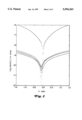
- FIG. 2 presents plots of current versus voltage for TMA-SnSe-1.
- this invention deals with nanoporous materials useful as a semiconductor in electronic devices and a process for modifying the band gap of these materials. Accordingly, one necessary component of this invention is a semiconducting nanoporous material. These materials are selected from the group consisting of metal polychalcogenides, metal oxides having the hollandite, psilomelane, todorakite structures or intergrowth of those structure, metal sulfide or selenide compounds and metal oxysulfide compounds.
- All of these materials are characterized in that they have a crystallographically-ordered nanoporous framework structure in which the cationic atoms (metals) are connected by bridging anionic species, i.e., sulfur, selenium, polysulfide, polyselenide, or oxygen.
- bridging anionic species i.e., sulfur, selenium, polysulfide, polyselenide, or oxygen.
- These materials have an intracrystalline pore system whose pores have an average pore diameter of about 2.5 to about 30 ⁇ . Most of these materials contain at least one structure directing agent in its pores.
- One group of nanoporous materials has the empirical formula expressed as xR:MA 2 ⁇ 0.2 :zH 2 O where x has a value of greater than 0 to about 1.0, R represents at least one organic structure-directing agent present in the intracrystalline pore system, M is germanium, tin, or combinations thereof, A is sulfur, selenium, or combinations thereof, z has a value of about 0 to about 4.0.
- these materials are synthesized by hydrothermal crystallization for an effective time at an effective pressure and temperature from a reaction mixture containing a reactive source of the metal, e.g., metal sulfide or selenide, a structure directing component, water and/or an organic solvent and an anion, e.g., bisulfide, hydroxide, etc.
- the structure directing agent can be a compound of an element of Group VA of the Periodic Table of the Elements, particularly nitrogen, phosphorus, arsenic and antimony, preferably nitrogen or phosphorus and most preferably nitrogen where such compounds also contain at least one alkyl or aryl group having from 1 to 8 carbon atoms.
- Polymeric quaternary ammonium salts such as [(C 14 H 32 N 2 )(OH) 2 ] x wherein "x" has a value of at least 2 are also suitably employed.
- the mono-, di- and triamines are advantageously utilized, either alone or in combination with a quaternary ammonium compound or other structure-directing compound. Mixtures of two or more structure-directing agents can either produce mixtures of the desired metal sulfides or the more strongly directing structure-directing species may control the course of the reaction with the other structure-directing agents serving primarily to establish the pH conditions of the reaction mixture.
- Representative structure-directing agents include: tetramethylammonium ions, tetraethylammonium ions, tetrapropylammonium ions, tetrabutylammonium ions, tetrapentylammonium ions, di-n-propylamine, ethylbutylamine, tripropylamine, triethylamine, triethanolamine, piperidine, cyclohexylamine, 2-methylpyridine, N,N-dimethylbenzylamine, N,N-dimethylethanolamine, choline, N,N'-dimethylpiperazine, 1,4-diazabicyclo(2,2,2,)octane, N-methyldiethanolamine, N-methylethanolamine, N-methylpiperidine, 3-methylpiperidine, N-methylcyclohexylamine, 3-methylpyridine, 4-methylpyridine, quinuclidine, N,N'-dimethyl-1,4-diazabic
- reaction mixture is prepared which has the composition, expressed in terms of molar ratios of:
- finely divided tin can be slurried with a quaternary ammonium compound such as tetramethylammonium hydroxide and mixed with finely divided sulphur or selenium. The resulting mixture is then heated at a reaction temperature of about 50° C. to about 200° C. for a time of about 2 to about 700 hours under autogenous pressure to give the desired nanoporous material.
- This process has the advantage that simpler materials can be used as the starting materials versus the metal sulfide or selenide materials used in the '761 patent. Applicants have aim found that this process yields products having large crystals on the order of 100 micrometers to about 4 mm. It has also been found that after reaction is complete, if the mixture is slowly cooled from the reaction temperature to room temperature at a cooling rate from about 1° to about 30° C./hour, larger crystals are obtained.
- a subclass of the metal sulfide or selenides described above are those having the empirical formula
- M' is a metal selected from the group consisting of thallium, silver, lead, mercury, chromium, arsenic, antimony, indium, molybdenum, tungsten, cobalt, zinc, copper, manganese, iron, nickel, cadmium and gallium.
- Preferred metals may be selected from the group consisting of molybdenum, tungsten, arsenic, antimony, indium, cobalt, zinc, manganese, iron, nickel, copper, cadmium and gallium, while especially preferred metals may be selected from the group consisting of cobalt, zinc, manganese, iron, nickel, copper, cadmium and gallium.
- the method of preparing these materials are also presented in the '761 patent.
- Metal oxysulfide compositions are another class of compounds which are useful as semiconductors. These materials are described in U.S. Pat. No. 5,122,357 which is incorporated by reference. As stated in the '357 patent these materials are described by the empirical formula
- Illustrative of the M" metals are cobalt, tin, zinc, iron, chromium, manganese, germanium, gallium and arsenic.
- polychalcogenide compounds which can be used in this invention are the polyselenide compounds having the formula (Ph 4 P)M1(Se 6 ) 2 where Ph represents a phenyl group and M1 is gallium, indium or thallium. These materials have been described by S. Dhingra and M. G. Kanatzidis, Science, Vol. 258, pp. 1769-1772 (1992). This reference also describes the preparation of these materials which involves mixing the metal (in elemental form) with (Ph 4 P) 2 Se 5 and elemental selenium, heating the mixture at about 200° C. for about 2 days to obtain the desired products.
- metal oxides with the hollandite, psilomelane or todorokite structure as well as intergrowth of these structures can be used.
- the metals may be selected from the group consisting of manganese, molybdenum, titanium, germanium, rhenium, zirconium, tin, antimony, aluminum, scandium, gallium, ruthenium, indium, chromium, iron, magnesium, cobalt, nickel, lithium and mixtures thereof.
- Examples of these materials are: Ba 3a Li.sub.(2a+4b) Ti.sub.(8-2a-b) O 6 where 0.32 ⁇ a ⁇ 0.42 and 0 ⁇ b ⁇ 0.20; Cs C TiO 2 where 0.125 ⁇ c ⁇ 0.22; K 1 .8 M2 0 .9 Ti 7 .1 O 16 where M2 is aluminum, chromium, iron, magnesium, cobalt and nickel; (Mg 0 .77 Na 0 .03)(Mg 0 .18 Mn +2 0 .60 Mn +4 5 .22)O 12 ⁇ 3.07 H 2 O.
- the synthesis of these materials is reported in the following references: J. Mater. Chem., 2(10), 993-996 (1992); Mat. Res. Bull., 25, 139-148 (1990); Mat. Res. Bull., 18, 203-210 (1983); Science, 231, 717-719 (1986).
- these nanoporous materials act as semiconductors.
- the band gap of these materials can vary from greater than 0 to about 5 eV and preferably from greater than 0 to about 3.5 eV.
- This band gap can be tuned or changed by varying the concentration of the structure-directing agent or by exchanging or replacing the structure-directing agent with mixtures of other cations and space-filling moieties, such as organic or inorganic cations and amines, alcohols, glycol, and water.
- the concentration of the structure-directing agent can be decreased by heating the nanoporous material at a temperature of about 50° C. to about 350° C. for a time of about 1 hr. to about 96 hr.
- the heating should be done under vacuum.
- the types of semiconducting devices in which the nanoporous materials of this invention can be used are well known in the art. Examples of these devices include doped and Schottky barrier diodes; light emitting diodes (LEDs); solar cells; tunnel diodes; photo diodes; bipolar transistors; field effect transistors (FETs); semiconductor-controlled rectifiers (SCRs); bilateral diode and triode switches (TRIACs); acoustic wave devices; semiconducting lasers; single and multiple quantum well and surface emitting lasers; semiconducting conductometric sensors; FET-based chemical sensors; self-elecro-optic-effect (SEED) devices.
- LEDs light emitting diodes
- FETs field effect transistors
- SCRs semiconductor-controlled rectifiers
- TRIACs bilateral diode and triode switches
- the nanoporous material can be the "p” semiconductor with the "n” semiconductor being a conventional semiconductor.
- the “n” semiconductor can be the nanoporous material while the “p” semiconductor is a conventional semiconductor.
- the nanoporous material can be both the “p” and the “n” semiconductor. It is understood that in this situation the nanoporous material which is the "p” semiconductor is different from the one which is the "n” semiconductor.
- the conventional semiconductors which can be used in these semiconductor devices are any of those well known in the art, examples of which are silicon, germanium, a III-V semiconductor and II-VI semiconductor. Specific examples of III-V semiconductors include GaAsInP and GaP. Specific examples of II-VI semiconductors include CdSe, CdTe and HgTe.
- the nanoporous materials of this invention can be used in a process for detecting the presence of molecular species in an environment. For example, the humidity or CO 2 level in a room or a gas stream can be monitored by using crystals of SnS-1 (SnS-1 is nomenclature for tin sulfide structure type 1 as set forth in U.S. Pat. No. 4,880,761).
- the process involves placing a molecular discriminating sensor in an environment which environment contains several molecular species, e.g., water, carbon dioxide, carbon monoxide, volatile organic compounds, etc.
- the molecule discriminating sensors comprise at least one nanoporous material which selectively adsorbs at least one molecular species.
- This selective adsorption is based either on the size of the molecular species or on the polarity of the molecular species. Selective adsorption using nanoporous materials is described in U.S. Pat. No. 5,013,337 which is incorporated by reference.
- the adsorption of molecular species by the nanoporous materials of this invention gives rise to a change in the optical and/or electronic properties of the material.
- This change can be detected by means well known in the art, and which means are attached to the molecule discriminating sensor.
- the sensor and means for detecting changes in the sensor make up a molecule discriminating device.
- a single crystal of the nanoporous semiconductor SnS-1 can be connected by leads placed directly on the crystals to an electrical circuit capable of detecting changes in conductivity.
- This molecule discriminating device can then be placed in an environment and used to monitor humidity or CO 2 levels.
- the CO 2 or water will be adsorbed by the SnS-1 crystal which then changes the conductivity of the SnS-1 crystal and which change is detected by the electronics associated with the device.
- Examples of other molecular species which can be detected by the process of this invention include H 2 S, COS, arsine, phosphine, oxygen, hydrocarbons, etc.
- Mixtures A, B and C gave products which were identified as SnS-1, SnS-4 and ZnSnS-4 respectively, by x-my diffraction analysis.
- tin-sulfide/selenide nanoporous materials were prepared. All of these materials had the x-my diffraction pattern of structure type 1 (SnS-1). These materials were prepared from a reaction mixture having the following formula:
- the tin source was finely divided tin, while the sulfur source was finely divided sulfur.
- Each mixture was placed in a Teflon®-lined stainless steel reactor and heated at about 150° C. under autogenous pressure for a time of 4 to 18 days. At this time the reactor was cooled and the product suction filtered and washed with water and acetone.
- X-ray powder diffraction analysis of the products revealed the presence of nanoporous fin chalcogenide structure type 1 as indicated in U.S. Pat. No. 4,880,761.
- Analytical data, summarized in Table 1 was acquired by quantitative SEM-EDX measurements. The empirical formula of these four materials was found to be: SnS-1, SnS 0 .43 Se 0 .57 -1, SnS 0 .22 Se 0 .78 -1, SnSe-1.
- band gaps were analyzed by UV-Visible reflectance spectroscopy and band gap energies computed which are presented in Table 1.
- the nature of the band gap can be measured using reflectance spectroscopy and a suitable light source, by determining the absorption edge and the functional dependence of the absorption coefficient on the photon energy.
- the radiation associated with this range of band gaps stretches from the UV to the near IR regions of the electromagnetic spectrum.
- reaction mixture was prepared by diluting 5.33 g of tetrapropylammonium (TPAOH) solution (obtained from Aldrich) with 3.71 g of water. To this solution there were added 0.34 g of elemental sulfur and then 0.63 g of tin metal powder. This gave a reaction mixture composition of
- the effect of the concentration of the organic templating agent on the band gap was determined by taking a tin sulfide nanoporous material prepared according to Example 20 of U.S. Pat. No. 4,880,761 using t-butylamine as the templating agent. This material had the structure SnS-1. Removal of the organic cation was carried out at 50° C. for 3 hours and 120° C. for 5 hours. UV reflectance spectroscopy (as described in Example 2) was used to measure the bandgaps of the materials, without exposure to air. It was observed that the band gap as evidenced by the absorption edge in the UV spectrum decreased by 10 and 30 nm respectively for the two treatments.
- TMA-SnSE-1 was prepared as per Example 2.
- a 1/4 inch tube of 99.8% pure Al 2 O 3 was used as a substrate for depositing the TMA SnSe-1.
- Two shallow grooves, 1 mm apart were cut into the tubes and 25 mil gold wires were wrapped tightly around the grooves.
- a slurry of the TMA-SnSe-1 in acetone was prepared and applied to the substrate tubes until a thickness of 1 mm was obtained.
- the conductivity of the sample was measured using the two probe dc conductivity method in which a constant voltage or current is impressed across the sample and voltage across and current through the sample are measured.
- nanoporous materials of this invention can adsorb molecular species, which adsorption produces an electrical change in the material.
Abstract
This invention relates to a semiconductor device comprising at least one p-n junction. The junction is formed from a "p" semiconductor contacting an "n" semiconductor. Said device characterized in that at least one of said "p" or "n" semiconductor is a nanoporous crystalline semiconducting material. These nanoporous materials have an intracrystalline nanopore system whose pores are crystallographically regular and have an average pore diameter of about 2.5 to about 30 Å. Additionally, they have a band gap of greater than 0 to about 5 eV which band gap can be modified by removing a portion of the templating agent from the pore system of the materials. The materials which have these properties include, metal polychalcogenide compounds, metal sulfides and selenides, metal oxides, and metal oxysulfides. These materials can be used in a large variety of semiconducting devices such as light emitting diodes, bipolar transistors, etc. A process for preparing these nanoporous materials is also presented.
Description
This application is a continuation-in-part of application, U.S. Ser. No. 08/329,388 filed Oct. 26, 1994, now abandoned, which in turn is a continuation-in-part of U.S. Ser. No. 08/037,965 filed Mar. 26, 1993, now abandoned, all of which is hereby incorporated.
This invention generally relates to semiconductor devices which have at least one p-n junction. Either the "p" or "n" (or both) semiconductors is a nanoporous semiconducting crystalline material. The nanoporous material is characterized in that it has an intracrystalline nanopore system whose pores are crystallographically regular and have an average pore diameter of about 2.5 Å to about 30 Å, and a band gap of greater than 0 to about 5 eV.
Semiconductor materials are used in numerous electronic applications including computers, sensors, and process control instrumentation. Increasing the speed of computers has necessitated the fabrication of increasingly smaller components coupled with the application of optical elements to more and more aspects of computer design. These technological prerequisites, as well as the need for better and more versatile sensors and process-control instrumentation, have brought with them requirements for semiconducting components with new or enhanced functionalities. The technological demands of high-speed computers have led to the development of techniques such as micromachining, vapor phase epitaxy, and nano-lithography, which allow the fabrication of increasingly smaller structures whereby bulk materials are engineered to provide submicron scale objects. Unfortunately, the technology required for molecule-discriminating devices such as sensors has not developed to the same advanced level. Most present-day molecule-discriminating devices contain one or more components composed of porous sintered aggregates of bulk semiconductors such as ZrO2 and SnO2. These materials have been described in the semiconducting art as "microporous", which describes the average dimensions of the random network of pores contained between the grains of the partially sintered component.
The term "microporous" has also been used in the semiconductor art to describe silicon metal that has been anodically etched in hydrofluoric acid so that only filamentous regions of nanometer dimensions remain. For example, Lehmann and Gosele describe the preparation of porous silicon. See Adv. Mater. 4(2), pp. 114-116 (1992). Evidence suggests that quantum confinement of electrons takes place in these silicon nanofilaments. Quantum confinement in semiconductors allows applications in LEDs, superlattice and quantum well lasers and other devices.
Applicants have taken a different approach to the design of new semiconducting functionalities which involves the use of crystalline materials that are nanoporous. By nanoporous is meant a material which has a crystallographically regular intracrystalline pore system whose pores have an average diameter of 2.5 to about 30 Å. Zeolites are the best known nanoporous materials. Zeolites are materials which have a three-dimensional framework structure composed of aluminum, silicon, and oxygen and an intracrystalline pore system. The intracrystalline pore system may have pores in one, two or three crystallographic directions. The unique feature of these materials is that the pores in any one direction are crystallographically ordered. Other examples of crystalline nanoporous materials include aluminophosphates, silicoaluminophosphates, germanium and tin-based metal sulfides and selenides, and zinc phosphates. See U.S. Pat. Nos. 4,310,440; 4,440,871; 4,880,761 and 5,126,120, respectively.
Applicants have found that a subclass of these molecular sieves have semiconducting properties. In particular, they are characterized in that they have an optical band gap of greater than zero to about 5 eV. Because of their nanoporosity, these semiconducting materials can be used in molecule discriminating electronic and optoelectronic devices (as well as other electronic and optoelectronic devices), in which a conventional semiconductor is replaced by a nanoporous structure to allow a molecule discriminating electronic or optical response to the presence of physisorbed and chemisorbed molecular and ionic species.
The effects of physisorbed species on the electronic properties of a dense semiconductor is usually negligible. The attractive forces involved in physisorption are generally of the dipole and induced-dipole type and usually follow simple Lennard-Jones r-6 energy dependence. The adsorbing surface will undergo some slight polarization with minimum penetration into the adsorbent. Physisorption within a nanoporous semiconductor induces a polarization that will affect the electronic properties to a much greater magnitude than any bulk or microcrystalline semiconductor. A nanoporous semiconductor is in principal a three-dimensional surface that is only a few atoms thick between adsorption sites in adjacent void spaces. The volume percent of this type of semiconductor that is polarized is essentially proportional to the fraction of the atoms that are on the intracrystalline surface. The net effect of physisorption is a magnification of the polarization relative to dense semiconductors and a corresponding perturbation of the electronic properties.
Electronic perturbations will also occur in acid-base types of interactions or in electrostatic ion-dipole and ion-quadrupole interactions between adsorbates and nanoporous semiconductors. The semiconductor/adsorbate interactions outlined here would perturb the electronic properties of a nanoporous semiconductor in a measurable way.
Because of the weak or negligible electronic effects of physisorption in traditional dense, microcrystalline semiconductors, the materials have only been used in sensing devices where chemisorption or ionosorption takes place. The electrical properties of semiconductors can be profoundly affected by the presence of chemisorbed or ionosorbed species at the surface. The main reason for these effects is the limited number of charge carriers in intrinsic semiconductors and the resulting deep penetration of the space-charge layer when carders are trapped at the surface by chemisorbed electron acceptors or donors. The space-charge layer (the depth of which is called the Debye Length) arises from the transfer of charge to or from the chemisorbed molecule and the resulting potential radient that extends from the surface into the semiconductor. The Debye Length is usually characterized as the penetration depth corresponding to a potential barrier of 1/e times the surface potential value.
The Debye Length for semiconductors with band gaps of greater than 0.8 eV will be at least 5.6 Å. Larger band gap materials, a category that includes many nanoporous chalcogenides, will display much larger Debye Lengths of the space charge layer as a result of chemisorption. The Debye Length of a space charge layer associated with appreciable chemisorption would penetrate the entire volume of a nanoporous semiconducting material.
Sintered polycrystalline compacts of dense semiconductors, such as SnO2, are widely used as combustible gas sensors. Polycrystalline compacts are used to maximize the amount of surface in contact with the atmosphere. The principal of operation is the conductance response to ionosorption of O2 (to form O2 -) and the effect of reducible gases on the amount of adsorbed O2. The response of these semiconducting sensors is extremely dependent on the device fabrication technique and aging of the SnO2. Theoretical models for the function of these porous semiconducting sensors are based on random barrier networks and Schottky barrier conduction.
Random barrier networks are associated with the conductivity through variable radius intergrain "necks", formed during the sintering of the compacts. See, P. Romppainen and V. Lantto, J. Appl. Phys., 63, (1988), 5159-5165. The Schottky barrier model is characterized by surface potential barriers caused by O2 adsorption between the SnO2 grains. See, J. F. McAleer, P. T. Moseley, B. C. Tofield, and D. E. Williams, Bri. Ceram. Proc., 1985, 89-105. The electric conductivity is therefore a function of grain boundary characteristics in the Schottky model. Both of these models predict a drastic dependence of the device performance on the sintered microstructure of the semiconducting component.
Nanoporous semiconductors do not have a random network of barriers and their electrical response would be large enough to preclude the necessity for a large external surface area. The interconnections between secondary building units are crystallographically regular, rather than random, and are a function of the framework topology rather than the fabrication history. A sensing device could be based on a single crystal of a nanoporous semiconductor. Besides the advantage of miniaturization, nanoporous semiconductors can be used to detect or discriminate physisorbed species as well as chemisorbed species, because of the magnitude of the sorption-induced electronic effects.
The nanoporous materials which possess semiconducting properties include the chalcogenide (sulfur, selenium, or combinations thereof) materials described in U.S. Pat. No. 4,880,761 and the oxysulfide materials of U.S. Pat. No. 5,122,357. Other materials are polychalcogenides (sulfur and selenium) compounds of group VIII, IIB, IIIB, IVB and VB of the Periodic Table of the Elements, as well as metal oxides hollandite, psilomelane, and todorokite pore structures, or intergrowths of the structures.
The above-named materials can be prepared hydrothermally with the aid of a structure-directing cation, by solid state high temperature methods or in molten salt media. After crystallization, these nanoporous materials will contain at least some structure directing agent or cations in the intracrystalline pore system. Applicants have found that the band gap of these materials can be modified by changing the concentration of the structure-directing agent present in the nanoporous material.
The art contains reports of "framework" materials that have semiconducting properties. For example, S. Dhingra and M. G. Kanatzidis in Science, Vol. 258, pp. 1769-72 (1992) report that materials such as (Ph4 P)(M)(Se6)2 have semiconducting properties. There are also reports of various metal oxides with the hollandite structure having semiconducting properties. These are: 1) Mat. Res. Bull., 25, 139-148 (1990); 2) Mat. Res. Bull., 18, 203-210 (1983); and 3) J. Mater. Chem., 2(10), 993-996 (1992).
Finally, U.S. Pat. No. 5,151,110 discloses using zeolites to adsorb chemical entities which gives rise to a mass change which change is detected by a piezoelectric substrate.
As stated, this invention deals with a semiconductor device containing a nanoporous material. One specific embodiment of the invention is a semiconductor device comprising at least one p-n junction, said junction formed from a "p" semiconductor contacting an "n" semiconductor, where at least one of said "p" or "n" semiconductor is a nanoporous semiconducting crystalline material having a crystallographically ordered nanoporous framework structure, an intracrystalline pore system whose pores have an average pore diameter of about 2.5 to about 30 Å and a band gap of greater than zero to about 5 eV said material selected from the group consisting of a metal sulfide or selenide having an empirical formula expressed in molar ratios: xR:MA2±0.2 :zH2 O where x has a value of greater than 0 to about 1.0, R represents at least one organic structure-directing agent present in the intracrystalline pore system, M is germanium, tin, or combinations thereof, A is sulfur, selenium, or combinations thereof, z has a value of about 0 to about 4.0; a metal sulfide or selenide having the empirical formula xR:M1-y M'y A2±0.2 :zH2 O where x has a value of greater than 0 to about 1.0, R represents at least one organic structure-directing agent present in the intracrystalline pore system, M is germanium, tin, or combinations thereof, y varies from greater than 0 to about 0.5, M' is a metal selected from the group consisting of thallium, silver, lead, mercury, chromium, arsenic, antimony, indium, molybdenum, tungsten, cobalt, zinc, copper, manganese, iron, nickel, cadmium and gallium, A is sulfur, selenium, or combinations thereof, z has a value of about 0 to about 4.0; and a metal oxysulfide composition having the empirical formula
(M".sub.s Al.sub.t P.sub.u Si.sub.v)S.sub.w O.sub.2-w
where M" is selected from the group consisting of cobalt, tin, zinc, iron, chromium, manganese, germanium, gallium and arsenic, s is the mole fraction of M" and varies from greater than zero to about 1, t is the mole fraction of Al and varies from 0 to less than 0.5, u is the mole fraction of P and varies from 0 to about 0.5, v is the mole fraction of Si and varies from 0 to less than 0.5, w is the mole fraction of S and varies from greater than zero to about 2s and t, u and v are chosen such that when t is greater than zero, u is greater than zero and s+t+u+v=1 and the n semiconductor is a conventional n doped semiconductor selected from silicon, germanium, a III-V semiconductor and a II-VI semiconductor.
Another embodiment of the invention is a process for preparing a crystalline nanoporous material having an empirical formula expressed in molar ratios: xR:MA2±0.2 :zH2 O where x has a value of greater than 0 to about 1.0, R represents at least one organic structure-directing agent present in the intracrystalline pore system, M is germanium or tin, A is sulfur, selenium, or combinations thereof, z has a value of about 0 to about 4.0, the process comprising forming a reaction mixture having the composition, expressed in terms of molar ratios of: 1RD:M:qA:mH2 O where 1 has a value of about 0.25 to about 5, m has a value of about 12 to about 1000, q has a value of about 0.5 to about 10, D is an anion, at a temperature, pressure and time sufficient to form the crystalline composition, the process characterized in that the source of M is freely divided germanium, tin, or combinations thereof and the source of A is elemental sulfur, selenium, or combinations thereof.
This and other objects and embodiments will become more apparent after a more detailed description of the invention.
FIG. 1 presents three UV reflectance spectra for: a) SnS-1; b) SnS-4; and c) ZnSnS-4.
FIG. 2 presents plots of current versus voltage for TMA-SnSe-1.
As stated above, this invention deals with nanoporous materials useful as a semiconductor in electronic devices and a process for modifying the band gap of these materials. Accordingly, one necessary component of this invention is a semiconducting nanoporous material. These materials are selected from the group consisting of metal polychalcogenides, metal oxides having the hollandite, psilomelane, todorakite structures or intergrowth of those structure, metal sulfide or selenide compounds and metal oxysulfide compounds. All of these materials are characterized in that they have a crystallographically-ordered nanoporous framework structure in which the cationic atoms (metals) are connected by bridging anionic species, i.e., sulfur, selenium, polysulfide, polyselenide, or oxygen. These materials have an intracrystalline pore system whose pores have an average pore diameter of about 2.5 to about 30 Å. Most of these materials contain at least one structure directing agent in its pores.
One group of nanoporous materials has the empirical formula expressed as xR:MA2±0.2 :zH2 O where x has a value of greater than 0 to about 1.0, R represents at least one organic structure-directing agent present in the intracrystalline pore system, M is germanium, tin, or combinations thereof, A is sulfur, selenium, or combinations thereof, z has a value of about 0 to about 4.0. These materials are described in U.S. Pat. No. 4,880,761 which is incorporated by reference. As described in the '761 patent, these materials are synthesized by hydrothermal crystallization for an effective time at an effective pressure and temperature from a reaction mixture containing a reactive source of the metal, e.g., metal sulfide or selenide, a structure directing component, water and/or an organic solvent and an anion, e.g., bisulfide, hydroxide, etc. The structure directing agent can be a compound of an element of Group VA of the Periodic Table of the Elements, particularly nitrogen, phosphorus, arsenic and antimony, preferably nitrogen or phosphorus and most preferably nitrogen where such compounds also contain at least one alkyl or aryl group having from 1 to 8 carbon atoms. Polymeric quaternary ammonium salts such as [(C14 H32 N2)(OH)2 ]x wherein "x" has a value of at least 2 are also suitably employed. The mono-, di- and triamines are advantageously utilized, either alone or in combination with a quaternary ammonium compound or other structure-directing compound. Mixtures of two or more structure-directing agents can either produce mixtures of the desired metal sulfides or the more strongly directing structure-directing species may control the course of the reaction with the other structure-directing agents serving primarily to establish the pH conditions of the reaction mixture. Representative structure-directing agents include: tetramethylammonium ions, tetraethylammonium ions, tetrapropylammonium ions, tetrabutylammonium ions, tetrapentylammonium ions, di-n-propylamine, ethylbutylamine, tripropylamine, triethylamine, triethanolamine, piperidine, cyclohexylamine, 2-methylpyridine, N,N-dimethylbenzylamine, N,N-dimethylethanolamine, choline, N,N'-dimethylpiperazine, 1,4-diazabicyclo(2,2,2,)octane, N-methyldiethanolamine, N-methylethanolamine, N-methylpiperidine, 3-methylpiperidine, N-methylcyclohexylamine, 3-methylpyridine, 4-methylpyridine, quinuclidine, N,N'-dimethyl-1,4-diazabicyclo(2,2,2,)octane ion, di-n-butylamine, neopentylamine, di-n-pentylamine, diisopropylamine, t-butylamine, ethylenediamine, pyrrolidine, 2-imidazolidone, piperazine, hexane-1,6-diamine, decylamine, decane-1,10-diamine, hexamethylenetetraamine, and adamantanamine.
Another process used to prepare the metal sulfide/selenide nanoporous materials is to use the metal and sulfur, selenium, or combinations thereof in their elemental states. In this case a reaction mixture is prepared which has the composition, expressed in terms of molar ratios of:
kRD:M:qA;mH.sub.2 O
where k has a value of about 0.25 to about 5.0, m has a value of about 12 to about 1000 and q has a value of about 0.5 to about 10. The anion D is selected from the group consisting of OH--, SH--, HCO3 --, F--, and Sx -2 (x=1 to 8). For example, finely divided tin can be slurried with a quaternary ammonium compound such as tetramethylammonium hydroxide and mixed with finely divided sulphur or selenium. The resulting mixture is then heated at a reaction temperature of about 50° C. to about 200° C. for a time of about 2 to about 700 hours under autogenous pressure to give the desired nanoporous material. This process has the advantage that simpler materials can be used as the starting materials versus the metal sulfide or selenide materials used in the '761 patent. Applicants have aim found that this process yields products having large crystals on the order of 100 micrometers to about 4 mm. It has also been found that after reaction is complete, if the mixture is slowly cooled from the reaction temperature to room temperature at a cooling rate from about 1° to about 30° C./hour, larger crystals are obtained.
A subclass of the metal sulfide or selenides described above are those having the empirical formula
xR:M.sub.1-y M'.sub.y A.sub.2±0.2 :zH.sub.2 O
where y varies from greater than 0 to about 0.5 and M' is a metal selected from the group consisting of thallium, silver, lead, mercury, chromium, arsenic, antimony, indium, molybdenum, tungsten, cobalt, zinc, copper, manganese, iron, nickel, cadmium and gallium. These materials are also described in U.S. Pat. No. 4,880,761 which states that the M' metal is one that meets the criteria: 1) occurs in sulfide or selenide minerals of hydrothermal origin; b) exhibits stable aqueous thiometallate or selenometallate chemistry or forms stable bisulfide or biselenide complexes and c) gives a minimum framework charge from about 0 to about -1 per metal atom in a M1-y M'y A2±0.2 framework structure. Illustrative of the metals which meet these criteria are thallium, silver, lead, mercury, chromium, arsenic, antimony, indium, molybdenum, tungsten, cobalt, zinc, copper, manganese, iron, nickel, cadmium and gallium. Preferred metals may be selected from the group consisting of molybdenum, tungsten, arsenic, antimony, indium, cobalt, zinc, manganese, iron, nickel, copper, cadmium and gallium, while especially preferred metals may be selected from the group consisting of cobalt, zinc, manganese, iron, nickel, copper, cadmium and gallium. The method of preparing these materials are also presented in the '761 patent.
Metal oxysulfide compositions are another class of compounds which are useful as semiconductors. These materials are described in U.S. Pat. No. 5,122,357 which is incorporated by reference. As stated in the '357 patent these materials are described by the empirical formula
(M".sub.s Al.sub.t P.sub.u Si.sub.v)S.sub.w O.sub.2-w
where M" is at least one metal selected from the group consisting of metals which: 1) can be incorporated into the framework structure of a microporous molecular sieve and 2) form hydrolytically stable sulfides; s is the mole fraction of Al and varies from 0 to less than 0.5, u is the mole fraction of P and varies from 0 to about 0.5, v is the mole fraction of Si and varies from 0 to less than 0.5, w is the mole fraction of S and varies from greater than zero to about 2s and t, u and v are chosen such that when t is greater than zero u is greater than zero and s+t+u+v=1. Illustrative of the M" metals are cobalt, tin, zinc, iron, chromium, manganese, germanium, gallium and arsenic.
Examples of polychalcogenide compounds which can be used in this invention are the polyselenide compounds having the formula (Ph4 P)M1(Se6)2 where Ph represents a phenyl group and M1 is gallium, indium or thallium. These materials have been described by S. Dhingra and M. G. Kanatzidis, Science, Vol. 258, pp. 1769-1772 (1992). This reference also describes the preparation of these materials which involves mixing the metal (in elemental form) with (Ph4 P)2 Se5 and elemental selenium, heating the mixture at about 200° C. for about 2 days to obtain the desired products.
Finally, metal oxides with the hollandite, psilomelane or todorokite structure as well as intergrowth of these structures can be used. The metals may be selected from the group consisting of manganese, molybdenum, titanium, germanium, rhenium, zirconium, tin, antimony, aluminum, scandium, gallium, ruthenium, indium, chromium, iron, magnesium, cobalt, nickel, lithium and mixtures thereof. Examples of these materials are: Ba3a Li.sub.(2a+4b) Ti.sub.(8-2a-b) O6 where 0.32<a<0.42 and 0<b<0.20; CsC TiO2 where 0.125<c<0.22; K1.8 M20.9 Ti7.1 O16 where M2 is aluminum, chromium, iron, magnesium, cobalt and nickel; (Mg0.77 Na0.03)(Mg0.18 Mn+2 0.60 Mn+4 5.22)O12 ·3.07 H2 O. The synthesis of these materials is reported in the following references: J. Mater. Chem., 2(10), 993-996 (1992); Mat. Res. Bull., 25, 139-148 (1990); Mat. Res. Bull., 18, 203-210 (1983); Science, 231, 717-719 (1986).
As stated, these nanoporous materials act as semiconductors. The band gap of these materials can vary from greater than 0 to about 5 eV and preferably from greater than 0 to about 3.5 eV. This band gap can be tuned or changed by varying the concentration of the structure-directing agent or by exchanging or replacing the structure-directing agent with mixtures of other cations and space-filling moieties, such as organic or inorganic cations and amines, alcohols, glycol, and water. Thus, the concentration of the structure-directing agent can be decreased by heating the nanoporous material at a temperature of about 50° C. to about 350° C. for a time of about 1 hr. to about 96 hr. Preferably the heating should be done under vacuum.
The types of semiconducting devices in which the nanoporous materials of this invention can be used are well known in the art. Examples of these devices include doped and Schottky barrier diodes; light emitting diodes (LEDs); solar cells; tunnel diodes; photo diodes; bipolar transistors; field effect transistors (FETs); semiconductor-controlled rectifiers (SCRs); bilateral diode and triode switches (TRIACs); acoustic wave devices; semiconducting lasers; single and multiple quantum well and surface emitting lasers; semiconducting conductometric sensors; FET-based chemical sensors; self-elecro-optic-effect (SEED) devices.
In these devices the nanoporous material can be the "p" semiconductor with the "n" semiconductor being a conventional semiconductor. Alternatively the "n" semiconductor can be the nanoporous material while the "p" semiconductor is a conventional semiconductor. Finally, the nanoporous material can be both the "p" and the "n" semiconductor. It is understood that in this situation the nanoporous material which is the "p" semiconductor is different from the one which is the "n" semiconductor. The conventional semiconductors which can be used in these semiconductor devices are any of those well known in the art, examples of which are silicon, germanium, a III-V semiconductor and II-VI semiconductor. Specific examples of III-V semiconductors include GaAsInP and GaP. Specific examples of II-VI semiconductors include CdSe, CdTe and HgTe.
In terms of actually fabricating the device, one way this can be done is by depositing one or more layers of conventional semiconductors and conductor contact points on one or more single crystals or thin film of nanoporous semiconductors. See, e.g., G. H. Yousefi and M. K. Agarwal, J. Mat. Sci. Let., 12, pp. 1447-1449 (1993).
The nanoporous materials of this invention can be used in a process for detecting the presence of molecular species in an environment. For example, the humidity or CO2 level in a room or a gas stream can be monitored by using crystals of SnS-1 (SnS-1 is nomenclature for tin sulfide structure type 1 as set forth in U.S. Pat. No. 4,880,761). The process involves placing a molecular discriminating sensor in an environment which environment contains several molecular species, e.g., water, carbon dioxide, carbon monoxide, volatile organic compounds, etc. The molecule discriminating sensors comprise at least one nanoporous material which selectively adsorbs at least one molecular species. This selective adsorption is based either on the size of the molecular species or on the polarity of the molecular species. Selective adsorption using nanoporous materials is described in U.S. Pat. No. 5,013,337 which is incorporated by reference.
As stated earlier, the adsorption of molecular species by the nanoporous materials of this invention gives rise to a change in the optical and/or electronic properties of the material. This change can be detected by means well known in the art, and which means are attached to the molecule discriminating sensor. Together, the sensor and means for detecting changes in the sensor make up a molecule discriminating device. For example, a single crystal of the nanoporous semiconductor SnS-1 can be connected by leads placed directly on the crystals to an electrical circuit capable of detecting changes in conductivity. This molecule discriminating device can then be placed in an environment and used to monitor humidity or CO2 levels. The CO2 or water will be adsorbed by the SnS-1 crystal which then changes the conductivity of the SnS-1 crystal and which change is detected by the electronics associated with the device. Examples of other molecular species which can be detected by the process of this invention include H2 S, COS, arsine, phosphine, oxygen, hydrocarbons, etc.
The procedures found in U.S. Pat. No. 4,880,761 were used to prepare SnS-1 (Ex. 20a), SnS-4 (Ex. 23a) and ZnSnS-4 nanoporous molecular sieves. The procedure involved mixing freshly precipitated tin sulfide with an aqueous solution of tetramethylammonium bicarbonate or tetrapropylammonium hydroxide, and then heating the mixture at 150° C. under autogeneous pressure. The composition of the reaction mixtures expressed as molar oxide ratios were:
A) TMAHCO3 :SnS2 :33 H2 O (7 day reaction time)
B) TPAOH:SnS2 :84 H2 O (16 hours reaction time
C) TPAOH:SnS2 :0.01 Zn(CH3 COO)2 :84 H2 O (89 hours reaction time)
Mixtures A, B and C gave products which were identified as SnS-1, SnS-4 and ZnSnS-4 respectively, by x-my diffraction analysis.
These three samples were analyzed by UV reflectance spectroscopy to determine if they have optical band gaps in the semiconducting range. The absorption edge in the reflectance spectrum is used to determine the band gap. See, Phys. Stat. Sol., 38, 363-367 (1970). The spectra of SnS-1, SnS-4 and ZnSnS-4 are presented in the Figure, and are labeled as (a), (b) and (c) respectively.
A series of tin-sulfide/selenide nanoporous materials were prepared. All of these materials had the x-my diffraction pattern of structure type 1 (SnS-1). These materials were prepared from a reaction mixture having the following formula:
(CH.sub.3).sub.4 NOH:Sn:tS:(2-t)Se:33 H.sub.2 O
where t=2.0, 1.5, 1.0, 0.0.
The tin source was finely divided tin, while the sulfur source was finely divided sulfur. Each mixture was placed in a Teflon®-lined stainless steel reactor and heated at about 150° C. under autogenous pressure for a time of 4 to 18 days. At this time the reactor was cooled and the product suction filtered and washed with water and acetone. X-ray powder diffraction analysis of the products revealed the presence of nanoporous fin chalcogenide structure type 1 as indicated in U.S. Pat. No. 4,880,761. Analytical data, summarized in Table 1, was acquired by quantitative SEM-EDX measurements. The empirical formula of these four materials was found to be: SnS-1, SnS0.43 Se0.57 -1, SnS0.22 Se0.78 -1, SnSe-1.
These materials were analyzed by UV-Visible reflectance spectroscopy and band gap energies computed which are presented in Table 1. The nature of the band gap can be measured using reflectance spectroscopy and a suitable light source, by determining the absorption edge and the functional dependence of the absorption coefficient on the photon energy. Calculated values for band gaps as a function of the wavelength of the absorption edge (where 1 eV=8065 cm-1 can be used as a conversion factor) are as follows: 2480 nm=0.5 eV; 1240 nm=1 eV; 620 nm=2 eV; 413 nm=3 eV; 310 nm=4 eV, 248 nm=5 eV. The radiation associated with this range of band gaps stretches from the UV to the near IR regions of the electromagnetic spectrum.
              TABLE 1
______________________________________
Band Gap of SnS.sub.x Se.sub.1-x -1 Materials
Material       Band gap (eV)
______________________________________
SnS-1          3.06
SnS.sub.0.43 Se.sub.0.57 -1
               2.43
SnS.sub.0.22 Se.sub.0.78 -1
               2.16
SnSe-1         1.91
______________________________________
A reaction mixture was prepared by diluting 5.33 g of tetrapropylammonium (TPAOH) solution (obtained from Aldrich) with 3.71 g of water. To this solution there were added 0.34 g of elemental sulfur and then 0.63 g of tin metal powder. This gave a reaction mixture composition of
TPAOH:Sn:2S:84 H.sub.2 O
The mixture was sealed in a Teflon®-lined stainless steel pressure vessel and heated in an oven at 150° C., under autogenous pressure, for 3 days. Product crystals, up to 1 mm in length, were recovered by filtration, washed well and dried under ambient condition. X-ray powder diffraction analysis indicated the identity of the product to be SnS-3(a) by comparison with powder XRD data from U.S. Pat. No. 4,880,761.
The effect of the concentration of the organic templating agent on the band gap was determined by taking a tin sulfide nanoporous material prepared according to Example 20 of U.S. Pat. No. 4,880,761 using t-butylamine as the templating agent. This material had the structure SnS-1. Removal of the organic cation was carried out at 50° C. for 3 hours and 120° C. for 5 hours. UV reflectance spectroscopy (as described in Example 2) was used to measure the bandgaps of the materials, without exposure to air. It was observed that the band gap as evidenced by the absorption edge in the UV spectrum decreased by 10 and 30 nm respectively for the two treatments.
TMA-SnSE-1 was prepared as per Example 2. A 1/4 inch tube of 99.8% pure Al2 O3 was used as a substrate for depositing the TMA SnSe-1. Two shallow grooves, 1 mm apart were cut into the tubes and 25 mil gold wires were wrapped tightly around the grooves. A slurry of the TMA-SnSe-1 in acetone was prepared and applied to the substrate tubes until a thickness of 1 mm was obtained. The conductivity of the sample was measured using the two probe dc conductivity method in which a constant voltage or current is impressed across the sample and voltage across and current through the sample are measured.
Using this technique, a sample of TMA-SnSe-1 was tested. First the sample was heated to 100° C. in dry argon for several hours and then cooled to 25° C. Argon saturated with 3% water was introduced into the sample chamber and the I-V behavior monitored as a function of time. Plots of log (abs(I)) versus volts, V, where I is current in amps, are presented in FIG. 2. The plots show an increase in conductivity with time as evidenced by increasing or higher currents with the lapse of time. It appears that two separate phenomena may be responsible for the observed changes. The changes during the initial time period may be owing to the adsorption of water molecules in the pores of the TMA-SnSe-1, while the large changes observed later may be owing to the process of multilayer water deposition on the surface of the sample.
These data show that the nanoporous materials of this invention can adsorb molecular species, which adsorption produces an electrical change in the material.
Claims (12)
1. A semiconductor device comprising at least one p-n junction, said junction formed from a "p" semiconductor contacting an "n" semiconductor, where the "p" semiconductor is a nanoporous semiconducting crystalline material having a crystallographically ordered nanoporous framework structure, an intracrystalline pore system whose pores have an average pore diameter of about 2.5 to about 30 Å and a band gap of greater than zero to about 5 eV said material selected from the group consisting of a metal sulfide or selenide having an empirical formula expressed in molar ratios: xR:MA2±0.2 :zH2 O where x has a value of greater than 0 to about 1.0, R represents at least one organic structure-directing agent present in the intracrystalline pore system, M is germanium, tin, or combinations thereof, A is sulfur, selenium, or combinations thereof, z has a value of about 0 to about 4.0; a metal sulfide or selenide having an empirical formula of xR:M1-y M'y A2±0.2 :zH2 O where x has a value of greater than 0 to about 1.0, R represents at least one organic structure-directing agent present in the intracrystalline pore system, M is germanium, tin, or combinations thereof, y varies from greater than 0 to about 0.5, M' is a metal selected from the group consisting of thallium, silver, lead, mercury, chromium, arsenic, antimony, indium, molybdenum, tungsten, cobalt, zinc, copper, manganese, iron, nickel, cadmium and gallium, A is sulfur, selenium, or combinations thereof, z has a value of about 0 to about 4.0; and a metal oxysulfide composition having an empirical formula of
(M".sub.s Al.sub.t P.sub.u Sl.sub.v)S.sub.w O.sub.2-w
where M" is selected from the group consisting of cobalt, tin, zinc, iron, chromium, manganese, germanium, gallium and arsenic, s varies from greater than zero to about 1, t varies from 0 to less than 0.5, u varies from 0 to about 0.5, v varies from 0 to less than 0.5, w varies from greater than zero to about 2s and t, u and v are chosen such that when t is greater than zero, u is greater than zero and s+t+u+v=1 and the "n" semiconductor is a conventional semiconductor selected from the group consisting of silicon, germanium, a III-V semiconductor and a II-VI semiconductor.
2. The device of claim 1 where the nanoporous material is a metal sulfide or selenide having the empirical formula xR:MA2±0.2 :zH2 O.
3. The device of claim 1 where the nanoporous material is a metal sulfide or selenide having the empirical formula xR:M1-y M'yA2±0.2 :zH2 O.
4. The device of claim 1 where the nanoporous material is a metal oxysulfide composition having the empirical formula (M"s Alt Pu Siv)Sw O2-w.
5. A semiconductor device comprising at least one p-n junction, said junction formed from a "p" semiconductor contacting an "n" semiconductor, where the "n" semiconductor is a nanoporous semiconducting crystalline material having a crystallographically ordered noneporous framework structure, an intracrystalline pore system whose pores have an average pore diameter of about 2.5 to about 30 Å and a band gap of greater than zero to about 5 eV said material selected from the group consisting of a metal sulfide or selenide having an empirical formula expressed in molar ratios: XR:MA2±0.2 :zH2 O where x has a value of greater than 0 to about 1.0, R represents at least one organic structure-directing agent present in the intracrystalline pore system, M is germanium, tin, or combinations thereof, A is sulfur, selenium, or combinations thereof, z has a value of about 0 to about 4.0; a metal sulfide or selenide having an empirical formula of xR:M1-y M'y A2±0.2 :zH2 O where x has a value of greater than 0 to about 1.0, R represents at least one organic structure-directing agent present in the intracrystalline pore system, M is germanium, tin, or combinations thereof, y varies from greater than 0 to about 0.5, M' is a metal selected from the group consisting of thallium, silver, lead, mercury, chromium, arsenic, antimony, indium, molybdenum, tungsten, cobalt, zinc, copper, manganese, iron, nickel, cadmium and gallium, A is sulfur, selenium, or combinations thereof, z has a value of about 0 to about 4.0; and a metal oxysulfide composition having an empirical formula of
(M".sub.s Al.sub.t P.sub.u Si.sub.v)S.sub.w O.sub.2-w
where M" is selected from the group consisting of cobalt, tin, zinc, iron, chromium, manganese, germanium, gallium and arsenic, s varies from greater than zero to about 1, t varies from 0 to less than 0.5, u varies from 0 to about 0.5, v varies from 0 to less than 0.5, w varies from greater than zero to about 2s and t, u and v are chosen such that when t is greater than zero, u is greater than zero and s+t+u+v=1 and the "p" semiconductor is a conventional semiconductor selected from the group consisting of silicon, germanium, a III-V semiconductor and a II-VI semiconductor.
6. The device of claim 5 where the nanoporous material is a metal sulfide or selenide having the empirical formula xR:MA2±0.2 :zH2 O.
7. The device of claim 5 where the nanoporous material is a metal sulfide or selenide having the empirical formula xR:M1-y M'yA2±0.2 :zH2 O.
8. The device of claim 5 where the nanoporous material is a metal oxysulfide composition having the empirical formula (M"s Alt Pu Siv)Sw O2-w.
9. A semiconductor device comprising at least one p-n junction, said junction formed from a "p" semiconductor contacting an "n" semiconductor, where each of said "p" and "n" semiconductor is a nanoporous semiconducting crystalline material having a crystallographically ordered nanoporous framework structure, an intracrystalline pore system whose pores have an average pore diameter of about 2.5 to about 30 Å and a band gap of greater than zero to about 5 eV said material selected from the group consisting of a metal sulfide or selenide having an empirical formula expressed in molar ratios: xR:MA2±0.2 :zH2 O where x has a value of greater than 0 to about 1.0, R represents at least one organic structure-directing agent present in the intracrystalline pore system, M is germanium, tin, or combinations thereof, A is sulfur, selenium, or combinations thereof, z has a value of about 0 to about 4.0; a metal sulfide or selenide having an empirical formula of xR:M1-y M'y A2±0.2 ;zH2 O where x has a value of greater than 0 to about 1.0, R represents at least one organic structure-directing agent present in the intracrystalline pore system, M is germanium, tin, or combinations thereof, y varies from greater than 0 to about 0.5, M" is a metal selected from the group consisting of thallium, silver, lead, mercury, chromium, arsenic, antimony, indium, molybdenum, tungsten, cobalt, zinc, copper, manganese, iron, nickel, cadmium and gallium, A is sulfur, selenium, or combinations thereof, z has a value of about 0 to about 4.0; and a metal oxysulfide composition having an empirical formula of
(M".sub.s Al.sub.t P.sub.u Si.sub.v)S.sub.w O.sub.2-w
where M" is selected from the group consisting of cobalt, tin, zinc, iron, chromium, manganese, germanium, gallium and arsenic, s varies from greater than zero to about 1, t varies from 0 to less than 0.5, u varies from 0 to about 0.5, v varies from 0 to less than 0.5, w varies from greater than zero to about 2s and t, u and v are chosen such that when t is greater than zero, u is greater than zero and s+t+u+v=1.
10. The device of claim 9 where the nanoporous material is a metal sulfide or selenide having the empirical formula xR:MA2±0.2 :zH2 O.
11. The device of claim 9 where the nanoporous material is a metal sulfide or selenide having the empirical formula xR:M1-y M'yA2±0.2 :zH2 O.
12. The device of claim 9 where the nanoporous material is a metal oxysulfide composition having the empirical formula (M"s Alt Pu Siv)Sw O2-w.
Priority Applications (1)
| Application Number | Priority Date | Filing Date | Title |
|---|---|---|---|
| US08/468,892 US5594263A (en) | 1993-03-26 | 1995-06-06 | Semiconductor device containing a semiconducting crystalline nanoporous material |
Applications Claiming Priority (3)
| Application Number | Priority Date | Filing Date | Title |
|---|---|---|---|
| US3796593A | 1993-03-26 | 1993-03-26 | |
| US32938894A | 1994-10-26 | 1994-10-26 | |
| US08/468,892 US5594263A (en) | 1993-03-26 | 1995-06-06 | Semiconductor device containing a semiconducting crystalline nanoporous material |
Related Parent Applications (1)
| Application Number | Title | Priority Date | Filing Date |
|---|---|---|---|
| US32938894A Continuation-In-Part | 1993-03-26 | 1994-10-26 |
Publications (1)
| Publication Number | Publication Date |
|---|---|
| US5594263A true US5594263A (en) | 1997-01-14 |
Family
ID=26714665
Family Applications (1)
| Application Number | Title | Priority Date | Filing Date |
|---|---|---|---|
| US08/468,892 Expired - Lifetime US5594263A (en) | 1993-03-26 | 1995-06-06 | Semiconductor device containing a semiconducting crystalline nanoporous material |
Country Status (1)
| Country | Link |
|---|---|
| US (1) | US5594263A (en) |
Cited By (12)
| Publication number | Priority date | Publication date | Assignee | Title |
|---|---|---|---|---|
| WO2000052764A1 (en) * | 1999-02-26 | 2000-09-08 | Hahn-Meitner-Institut Berlin Gmbh | Electrochemical deposit from cuscn in porous tio2 films |
| US6465052B1 (en) | 2001-11-30 | 2002-10-15 | Nanotek Instruments, Inc. | Method for production of nano-porous coatings |
| WO2003060596A2 (en) * | 2001-10-24 | 2003-07-24 | The Regents Of The University Of California | Semiconductor liquid crystal composition and methods for making the same |
| US20030145779A1 (en) * | 2001-11-30 | 2003-08-07 | Regents Of The University Of California | Shaped nanocrystal particles and methods for making the same |
| US20050142769A1 (en) * | 2003-12-25 | 2005-06-30 | Yoshiki Kamata | Semiconductor device and method for manufacturing the same |
| US20060220058A1 (en) * | 2003-06-10 | 2006-10-05 | Avto Tavkhelidze | Multiple tunnel junction thermotunnel device on the basis of ballistic electrons |
| WO2014009061A3 (en) * | 2012-07-09 | 2014-07-31 | Robert Bosch Gmbh | Use of microporous anionic inorganic framework structures containing dopant cations for producing thin film solar cells |
| US20140252344A1 (en) * | 2013-03-07 | 2014-09-11 | Ricoh Company, Ltd. | P-type oxide composition, and method for producing p-type oxide composition |
| US9649622B1 (en) * | 2016-05-16 | 2017-05-16 | National Taiwan University Of Science And Technology | Bimetal oxysulfide solid-solution catalyst and manufacturing method thereof, method for carbon dioxide reduction, method for heavy metal reduction, and method for hydrogenation of organic compounds |
| US9771262B1 (en) | 2016-05-16 | 2017-09-26 | National Taiwan University Of Science And Technology | Method for organic compound degradation and method for producing hydrogen |
| US10379083B2 (en) * | 2016-01-04 | 2019-08-13 | Farshid Raissi | Electronic device for detection of viruses, bacteria, and pathogens |
| CN112624040A (en) * | 2020-12-22 | 2021-04-09 | 佛山(华南)新材料研究院 | Method for preparing hydrogen |
Citations (4)
| Publication number | Priority date | Publication date | Assignee | Title |
|---|---|---|---|---|
| US4310440A (en) * | 1980-07-07 | 1982-01-12 | Union Carbide Corporation | Crystalline metallophosphate compositions |
| US4440871A (en) * | 1982-07-26 | 1984-04-03 | Union Carbide Corporation | Crystalline silicoaluminophosphates |
| US5013337A (en) * | 1988-12-06 | 1991-05-07 | Uop | Process for separating a mixture of molecular species using crystalline microporous metal sulfide compositions |
| US5126120A (en) * | 1990-10-02 | 1992-06-30 | Uop | Crystalline microporous zinc phosphate compositions |
-
1995
- 1995-06-06 US US08/468,892 patent/US5594263A/en not_active Expired - Lifetime
Patent Citations (4)
| Publication number | Priority date | Publication date | Assignee | Title |
|---|---|---|---|---|
| US4310440A (en) * | 1980-07-07 | 1982-01-12 | Union Carbide Corporation | Crystalline metallophosphate compositions |
| US4440871A (en) * | 1982-07-26 | 1984-04-03 | Union Carbide Corporation | Crystalline silicoaluminophosphates |
| US5013337A (en) * | 1988-12-06 | 1991-05-07 | Uop | Process for separating a mixture of molecular species using crystalline microporous metal sulfide compositions |
| US5126120A (en) * | 1990-10-02 | 1992-06-30 | Uop | Crystalline microporous zinc phosphate compositions |
Non-Patent Citations (2)
| Title |
|---|
| Yousefi et al., "Electrical Contacts to Chalcogenide Single Crystals", Journal of Materials Science Letters, vol. 12, 1993, pp. 1447-1449. |
| Yousefi et al., Electrical Contacts to Chalcogenide Single Crystals , Journal of Materials Science Letters, vol. 12, 1993, pp. 1447 1449. * |
Cited By (17)
| Publication number | Priority date | Publication date | Assignee | Title |
|---|---|---|---|---|
| WO2000052764A1 (en) * | 1999-02-26 | 2000-09-08 | Hahn-Meitner-Institut Berlin Gmbh | Electrochemical deposit from cuscn in porous tio2 films |
| WO2003060596A2 (en) * | 2001-10-24 | 2003-07-24 | The Regents Of The University Of California | Semiconductor liquid crystal composition and methods for making the same |
| WO2003060596A3 (en) * | 2001-10-24 | 2004-01-29 | Univ California | Semiconductor liquid crystal composition and methods for making the same |
| US6884478B2 (en) | 2001-10-24 | 2005-04-26 | The Regents Of The University Of California | Semiconductor liquid crystal composition and methods for making the same |
| US6465052B1 (en) | 2001-11-30 | 2002-10-15 | Nanotek Instruments, Inc. | Method for production of nano-porous coatings |
| US20030145779A1 (en) * | 2001-11-30 | 2003-08-07 | Regents Of The University Of California | Shaped nanocrystal particles and methods for making the same |
| WO2004111552A3 (en) * | 2003-06-10 | 2006-11-23 | Borealis Tech Ltd | Multiple tunnel junction thermotunnel device on the basis of ballistic |
| US20060220058A1 (en) * | 2003-06-10 | 2006-10-05 | Avto Tavkhelidze | Multiple tunnel junction thermotunnel device on the basis of ballistic electrons |
| US20050142769A1 (en) * | 2003-12-25 | 2005-06-30 | Yoshiki Kamata | Semiconductor device and method for manufacturing the same |
| US20080258264A1 (en) * | 2003-12-25 | 2008-10-23 | Yoshiki Kamata | Semiconductor device and method for manufacturing the same |
| WO2014009061A3 (en) * | 2012-07-09 | 2014-07-31 | Robert Bosch Gmbh | Use of microporous anionic inorganic framework structures containing dopant cations for producing thin film solar cells |
| US20140252344A1 (en) * | 2013-03-07 | 2014-09-11 | Ricoh Company, Ltd. | P-type oxide composition, and method for producing p-type oxide composition |
| US9396937B2 (en) * | 2013-03-07 | 2016-07-19 | Ricoh Company, Ltd. | P-type oxide composition, and method for producing P-type oxide composition |
| US10379083B2 (en) * | 2016-01-04 | 2019-08-13 | Farshid Raissi | Electronic device for detection of viruses, bacteria, and pathogens |
| US9649622B1 (en) * | 2016-05-16 | 2017-05-16 | National Taiwan University Of Science And Technology | Bimetal oxysulfide solid-solution catalyst and manufacturing method thereof, method for carbon dioxide reduction, method for heavy metal reduction, and method for hydrogenation of organic compounds |
| US9771262B1 (en) | 2016-05-16 | 2017-09-26 | National Taiwan University Of Science And Technology | Method for organic compound degradation and method for producing hydrogen |
| CN112624040A (en) * | 2020-12-22 | 2021-04-09 | 佛山(华南)新材料研究院 | Method for preparing hydrogen |
Similar Documents
| Publication | Publication Date | Title |
|---|---|---|
| US5594263A (en) | Semiconductor device containing a semiconducting crystalline nanoporous material | |
| Shooshtari et al. | Effect of temperature and humidity on the sensing performance of TiO2 nanowire-based ethanol vapor sensors | |
| Peng et al. | Design of semiconducting tetrahedral Mn 1− x Zn x O alloys and their application to solar water splitting | |
| Shouli et al. | Different morphologies of ZnO nanorods and their sensing property | |
| Nimbalkar et al. | Synthesis of highly selective and sensitive Cu-doped ZnO thin film sensor for detection of H2S gas | |
| Zhou et al. | Room temperature ozone sensing properties of p-type CuCrO2 nanocrystals | |
| Wlaźlak et al. | Heavy pnictogen chalcohalides: the synthesis, structure and properties of these rediscovered semiconductors | |
| CN109891601A (en) | Sulfide film, the device including it and the method that forms the film | |
| Punetha et al. | Enhancement and optimization in sensing characteristics of ammonia gas sensor based on light assisted nanostructured WO 3 thin film | |
| Huo et al. | Phase-and size-controllable synthesis with efficient photocatalytic activity of ZnS nanoparticles | |
| Hassan et al. | Fe dopants enhancing ethanol sensitivity of ZnO thin film deposited by RF magnetron sputtering | |
| Scalvi et al. | Transient decay of photoinduced current in semiconductors and heterostructures | |
| Ashok | Growth and characterization of CdS thin films by chemical bath deposition | |
| Su et al. | Tin dioxide functionalized single-walled carbon nanotube (SnO2/SWNT)-based ammonia gas sensors and their sensing mechanism | |
| Arifin et al. | MOCVD growth and characterization of TiO2 thin films for hydrogen gas sensor application | |
| Subedi et al. | Near infrared to ultraviolet optical properties of bulk single crystal and nanocrystal thin film iron pyrite | |
| Sathya et al. | Effect of zirconium doping on ZnO nanostructured thin films and the enhanced ammonia gas sensing activity | |
| Suhail et al. | Characterization and NO2 gas sensing performance of CdO: In2O3 polycrystalline thin films prepared by spray pyrolysis technique | |
| Rusu et al. | Deposition and characterization of Ga2Se3 thin films prepared by a novel chemical close-spaced vapour transport technique | |
| Gaur et al. | Enhancement of photosensitivity of thermally evaporated crystalline PbS thin films by low energy oxygen ions implantation | |
| Mukherjee et al. | Interplay between Growth Mechanism, Materials Chemistry, and Band Gap Characteristics in Sputtered Thin Films of Chalcogenide Perovskite BaZrS3 | |
| Parlak et al. | Growth, electrical and structural characterization of β-GaSe thin films | |
| Fendler | Size‐Quantized Semiconductor Particulate Films Generated in situ at Monolayers | |
| Bai et al. | Synthesis of 1D ZnO Crystals and Sensing Properties for ${\rm NO} _ {2} $ Gas | |
| Ganguly et al. | CdS Quantum Dots Based Nano Light Emitting Device |
Legal Events
| Date | Code | Title | Description |
|---|---|---|---|
| AS | Assignment |
Owner name: UOP, ILLINOIS Free format text: ASSIGNMENT OF ASSIGNORS INTEREST;ASSIGNORS:BEDARD, ROBERT L.;OZIN, GEOFFREY A.;AHARI, HOMAYOUN;AND OTHERS;REEL/FRAME:008180/0149;SIGNING DATES FROM 19950524 TO 19950605 |
|
| STCF | Information on status: patent grant |
Free format text: PATENTED CASE |
|
| CC | Certificate of correction | ||
| FPAY | Fee payment |
Year of fee payment: 4 |
|
| FPAY | Fee payment |
Year of fee payment: 8 |
|
| FPAY | Fee payment |
Year of fee payment: 12 |