US5583749A - Baseboard and daughtercard apparatus for reconfigurable computing systems - Google Patents
Baseboard and daughtercard apparatus for reconfigurable computing systems Download PDFInfo
- Publication number
- US5583749A US5583749A US08/348,280 US34828094A US5583749A US 5583749 A US5583749 A US 5583749A US 34828094 A US34828094 A US 34828094A US 5583749 A US5583749 A US 5583749A
- Authority
- US
- United States
- Prior art keywords
- daughtercards
- array
- electrical connectors
- baseboard
- daughtercard
- Prior art date
- Legal status (The legal status is an assumption and is not a legal conclusion. Google has not performed a legal analysis and makes no representation as to the accuracy of the status listed.)
- Expired - Lifetime
Links
Images


Classifications
-
- H—ELECTRICITY
- H05—ELECTRIC TECHNIQUES NOT OTHERWISE PROVIDED FOR
- H05K—PRINTED CIRCUITS; CASINGS OR CONSTRUCTIONAL DETAILS OF ELECTRIC APPARATUS; MANUFACTURE OF ASSEMBLAGES OF ELECTRICAL COMPONENTS
- H05K7/00—Constructional details common to different types of electric apparatus
- H05K7/02—Arrangements of circuit components or wiring on supporting structure
- H05K7/023—Stackable modules
-
- H—ELECTRICITY
- H05—ELECTRIC TECHNIQUES NOT OTHERWISE PROVIDED FOR
- H05K—PRINTED CIRCUITS; CASINGS OR CONSTRUCTIONAL DETAILS OF ELECTRIC APPARATUS; MANUFACTURE OF ASSEMBLAGES OF ELECTRICAL COMPONENTS
- H05K1/00—Printed circuits
- H05K1/02—Details
- H05K1/0286—Programmable, customizable or modifiable circuits
-
- H—ELECTRICITY
- H05—ELECTRIC TECHNIQUES NOT OTHERWISE PROVIDED FOR
- H05K—PRINTED CIRCUITS; CASINGS OR CONSTRUCTIONAL DETAILS OF ELECTRIC APPARATUS; MANUFACTURE OF ASSEMBLAGES OF ELECTRICAL COMPONENTS
- H05K1/00—Printed circuits
- H05K1/02—Details
- H05K1/14—Structural association of two or more printed circuits
Definitions
- the present invention relates in general to circuit board apparatus used for implementing computing subsystems, and in particular to an apparatus including a baseboard and a family of reconfigurable daughtercards.
- PCBs Printed circuit boards
- Printed circuit boards facilitate rapid construction of electronic circuits by providing a stable insulating sheet of material upon which circuit components are mounted.
- the components are typically interconnected using thin plated conductive (e.g. copper) lines bonded to the sheet that form circuit paths.
- thin plated conductive (e.g. copper) lines bonded to the sheet that form circuit paths.
- FPDs Field programmable devices
- programmable device refers to once programmable as well as reprogrammable devices.
- FPD-based PCB One example of an FPD-based PCB is the "Anyboard” developed at North Carolina State University.
- the Anyboard consists of a hardware card that incorporates six FPDs (more specifically field programmable gate arrays, or FPGAs), three random access memory (RAM) chips, buffers and local and global buses that connect the FPGAs to the RAMs and buffers.
- FPDs more specifically field programmable gate arrays, or FPGAs
- RAM random access memory
- FPD-based PCBs such as the Anyboard provide flexibility in terms of the variety of circuits that can be developed, to the extent that the architecture of the board is fixed in hardware the application of the board is limited. In case of the Anyboard, for example, the number of FPGAs and RAMs as well as the bus interconnection are fixed in hardware. This also limits the user's ability to upgrade and expand the system's hardware.
- Altera Corporation of San Jose has developed a reconfigurable FPD-based universal circuit board (UCB) that provides significant improvements in terms of interconnect and architecture flexibility.
- the UCB includes a number of sockets that can receive FPDs, field programmable interconnect devices (FPIDs), or selective shorting circuits interchangeably.
- FPIDs field programmable interconnect devices
- Various inter-socket interconnect topologies and board interface alternatives provide further flexibility.
- the UCB is fully described in a commonly assigned patent application, Ser. No. 08/206,774 filed Mar. 4, 1994 now U.S. Pat. No. 5,537,295, which is hereby incorporated by reference in its entirety.
- the UCB incorporates a sizable amount of memory on board, to add more memory or other types of logic blocks requires separate additional boards. This is also true if the application requires more than the maximum number of gates available on the UCB.
- the present invention provides a rapid prototyping system that is made up of independent reconfigurable modules or daughtercards that are mounted on a baseboard or mothercard. Multiple daughtercards can be mounted on the baseboard in a planar or stacked fashion.
- the modular architecture allows for easy expansion and upgrade of the system.
- Each reconfigurable daughtercard in the prototyping system of the present invention is designed as a system independent module that can carry any combination of field programmable devices, memory circuits or any other type of functional block.
- the baseboard is then especially designed to accommodate system dependent factors for each particular application.
- Each reconfigurable daughtercard includes an internal bus network to interconnect its various components as well as a special input/output array of connectors.
- the daughtercard may be either single-sided or double-sided (i.e., carrying components on both sides of the card) for maximum use of space.
- Complementary arrays of connectors are provided on daughtercards and baseboards to allow a daughtercard to mount on a baseboard or to stack vertically on top of another daughtercard. The system hardware can therefore be easily expanded by adding more daughtercards as required.
- the modular design of the prototyping system of the present invention allows simple, incremental upgrade of installed boards by adding to or replacing daughtercards, and allows simple migration to new systems by changing the baseboard.
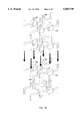
- FIG. 1A illustrates one side of an exemplary daughtercard according to the present invention
- FIG. 1B shows a three dimensional view of an exemplary bussing arrangement within a daughtercard as well as between two stacked daughtercards;
- FIGS. 2A and 2B show two examples of a baseboard carrying several daughtercards in a planar and stacked fashion
- FIG. 3 shows the busing between a baseboard and daughtercards according to one embodiment of the present invention.
- FIGS. 4A, 4B, and 4C illustrate examples of various applications for daughtercards.
- the top side of an exemplary daughtercard 100 for the prototyping system of the present invention includes four field programmable devices (FPDs) 102, two memory devices 104, and four connector pad arrays 106.
- the bottom side is a mirror image of the top side, doubling the total count of the components.
- An alternative embodiment of the daughtercard may replace the central array of connector pads with more memory devices.
- the embodiment shown in FIG. 1 with higher I/O count may be preferable since in applications where larger memory is needed a dedicated memory daughtercard can easily be added to the system.
- Daughtercard 100 includes internal busing (not shown) that interconnects its various components.
- Each memory device 104 connects to two adjacent FPDs 102 in a manner similar to that described in application Ser. No. 08/206,774 filed Mar. 4, 1994 now U.S. Pat. No. 5,537,295, while FPDs 102 interconnect in a nearest-neighbor cube.
- the nearest-neighbor cube arrangement provides direct connection between each FPD 102 and its two adjacent neighbors as well as the FPD located directly under it.
- More complicated busing arrangements are made possible by stacking a special busing card above daughtercard 100.
- Such busing card may include wiring traces that connect pins from connector pad array 106 to reproduce various interconnect topologies, several examples of which are described in the above-cited application Ser. No. 08/206,774.
- FPD 102 The type of FPD 102 used depends on the application. High density FPDs such as Altera FLEX81500 provide higher input/output (I/O) pin count (a total of 313 I/O pins) and more capacity, while parts such as Altera FLEX81188 provide a lower cost alternative with fewer I/Os.
- memory devices 104 can be either large (e.g., 512 K ⁇ 8) synchronous random access memories (SRAMs), or any one of a variety of smaller and faster memory circuits.
- FIG. 2A illustrates one example of how a number of daughtercards 100 may be mounted on one side of a baseboard 200 in the prototyping system of the present invention.
- the particular example shown in FIG. 2A includes a baseboard 200 that can carry, for example, three adjacently mounted daughtercards 100 on one side.
- An exploded view of stacking of daughtercards 100 is also shown.
- Daughtercards 100 shown in FIG. 2A do not include the central array of pads and are an alternative embodiment to that shown in FIG. 1. This embodiment can accommodate larger components on its surface, while the embodiment shown in FIG. 1 provides more flexibility as it can be divided into two identical halves.
- Baseboard 200 of this embodiment thus includes two connector pad arrays 202 on either side along the length of the board.
- Special connectors 204 connect pad arrays 106 on each daughtercard 100 to pad arrays 202 on baseboard 200, or to pad arrays 106 on other daughtercards 100 when stacked.
- FIG. 2B shows yet another embodiment of the daughtercard/baseboard system of the present invention.
- each daughtercard 100 includes three pad arrays 106, one along each edge and only one array in the center.
- Baseboard 200 also includes a corresponding central pad array, and in this example is shown as carrying two full-size daughtercards 100 and one half-size daughtercard 206.
- the option of using a half-size card allows a reduction in component and overall design cost.
- the daughtercards and the baseboard in this embodiment are connected by special connectors 204 as in the embodiment shown in FIG. 2A. It is to be understood that while both FIGS. 2A and 2B show mounting components on one side of baseboard 200, baseboard 200 may be double-sided allowing for a similar stacking of duaghtercards on a second side.
- connector 204 used for connecting to pad arrays 106 is critical to the overall performance of the system.
- Connector 204 should have high density and large bandwidth (high speed) with minimum crosstalk.
- the connection made by connector 204 should preferably be solderless and require low mating force.
- An example of a commercially available connector that provides a good compromise is the CIN::APSE connectors from Cinch Connectors.
- one third of these I/O terminals are used for power and ground connections, leaving about 1000 general purpose I/Os.
- CIN::APSE connectors use compressible fuzz-buttons to make contact with copper pads on the baseboard and daughtercards. To hold the board and the intervening connectors together, mounting screws are used that allow easy removal of connectors if no daughtercard is present.
- FIG. 3 illustrates a high level view of how the several buses are connected in a full system.
- a standard system bus 300 runs in parallel to every daughtercard 100 serially and provides a standard environment for daughtercards containing microprocessors and other common peripherals. This could be a user defined bus or any one of VMEbus, SBUS, ISA, etc.
- a dedicated configuration bus 302 threads through each daughtercard 100 and passes configuration data from the baseboard 200 to the stacks of daughtercards. Configuration files are downloaded to each reconfigurable element depending upon their order on the configuration bus.
- a third bus, JTAG bus 304 operates in a similar fashion to that of configuration bus 302.
- JTAG bus 304 can be used, for example, to identify the members of each stack via their JTAG ID codes, force test vectors into the system, single-step the system, and gather the results for debugging.
- a large fourth bus is provided as a free bus 306 that provides global and local I/O between reconfigurable daughtercards. Free buses 306 in each stack are independent, but baseboard 200 or the user may add application-specific wiring if a single stack is too small for a particular function.
- FIG. 3 also shows one example of the external interface circuitry for baseboard 200.
- An FPD 308 provides programmable interface to an external bus such as a PCI bus.
- An example of an FPD 308 that provides sufficient I/O to decode the 32-bit addresses passing over the PCI bus is the Altera FLEX8452 or Altera MAX7000.
- a second FPD 310 is also provided to control system bus 300, configuration bus 302, and JTAG bus 304 bus interfaces on baseboard 200.
- This chip also controls the gating of signals from system bus 300 onto the external bus of baseboard 200.
- a part such as Altera's FLEX81188 can implement SCSI interface as well as provide general-purpose I/O.
- Various baseboards 200 can be designed to accommodate different bus standards.
- the prototyping system of the present invention accommodates a large variety of daughtercards that can be mixed and matched by a user to build a particular subsystem to suit their requirement.
- the typical daughtercard which provides configurable logic and memory is shown in FIG. 1.
- FIGS. 4A, 4B, and 4C show several other examples of the types of daughtercards that can be built into the system of the present invention.
- FIG. 4A shows a dedicated double-sided memory daughtercard which includes 16 512 ⁇ 8 SRAM chips 400 on each side. This memory daughtercard provides 16 MByte of SRAM for memory intensive applications.
- FIG. 4B shows a hobby (low-cost) daughtercard with four 84-pin PLCC sockets 402 on one side.
- This daughtercard could also include two sockets for memory devices, and provides a low-cost board for hobbyists who can populate the board starting with, for example, one FLEX8282 part and incrementally upgrading to larger projects.
- This card is different from the others in that instead of using surface mount components where the components are hard-soldered to the card, sockets are provided to facilitate easy modifications to the board. Because the socket connectors go through the card, the hobby daughtercard shown in FIG. 4B is a single-sided card. Other examples of daughtercards may provide surface mount sockets for more flexibility.
- FIG. 4C shows a cable daughtercard that includes six 80-pin nanoconnectors 404 on one side. This card can bring 480 signals to an outside prototyping area through six nanocables. All the daughtercards shown in FIGS. 4A, 4B, 4C are the type that include two identical halves, with arrays of conductor pads on the edges as well as in the center of the card.
- a major class of applications for the system of the present invention is as a programmable application accelerator.
- the board can be used in a computer system, for example, to speed up image processing algorithms or for speeding compression and decompression of digital data.
- application specific daughtercards include a CPU board accommodating CPU or DSP modules for incorporation into larger designs, a crossbar card including programmable interconnect layers or reconfigurable memory modules, a breadboarding card in the form of a double- or triple-wide daughtercard with large prototyping area to allow users to plug in various commercial chips to augment the logic on other daughtercards, etc.
- the baseboard/daughtercard system of the present invention may incorporate a variety of daughtercard types in a single apparatus.
- a single system may include a mix of double-sided cards with surface mount components (e.g., memory daughtercard) and single-sided socketed cards (e.g., hobby daughtercard) as well as cards with surface mount sockets.
- the total capacity of the prototyping system of the present invention is limited by factors such as size and power consumption. Assuming each CIN::APSE fuzz-button can handle 250 mA, a total current of approximately 31 A can be passed into a stack of daughtercards for the embodiment shown in FIG. 2B. This is enough current to power a stack of five daughtercards of the type used in the embodiment shown in FIG. 2B. Thus, a single baseboard 200 such as the one shown in FIG. 2B can house 10 full size daughtercards 100 and five half size daughtercards on each side, for a total capacity equal to 25 full size daughtercards for a double-sided baseboard. Given, for example, 100 k gates per daughtercard, such a board would provide a total of 2.5 million gates.
- CIN::APSE connectors define a channel for forced air cooling.
- Other newly developed fluorinate-based heat sinks can also be utilized to address the heat problem.
- the baseboard may be equipped with, for example, a compatible Molex connector so that the baseboard may be powered directly by connection to a personal computer's standard power supply. In that case, the baseboard would not receive its power from the system bus.
- the present invention provides an apparatus that includes a set of baseboards and a family of daughtercards, together with a programmable interface to an external bus for a host system.
- Daughtercards attach to the baseboard through complementary connectors mounted between the baseboard and the daughtercards.
- daughtercards are constructed to allow stacking of daughtercards vertically.
- the baseboard and daughtercard approach of the present invention allows simple, incremental upgrade of installed boards by adding or replacing the daughtercards and allows simple migration to new systems by changing baseboards.
Abstract
Description
Claims (25)
Priority Applications (2)
| Application Number | Priority Date | Filing Date | Title |
|---|---|---|---|
| US08/348,280 US5583749A (en) | 1994-11-30 | 1994-11-30 | Baseboard and daughtercard apparatus for reconfigurable computing systems |
| GB9524213A GB2296999B (en) | 1994-11-30 | 1995-11-27 | Baseboard and daughtercard apparatus for reconfigurable computing systems |
Applications Claiming Priority (1)
| Application Number | Priority Date | Filing Date | Title |
|---|---|---|---|
| US08/348,280 US5583749A (en) | 1994-11-30 | 1994-11-30 | Baseboard and daughtercard apparatus for reconfigurable computing systems |
Publications (1)
| Publication Number | Publication Date |
|---|---|
| US5583749A true US5583749A (en) | 1996-12-10 |
Family
ID=23367349
Family Applications (1)
| Application Number | Title | Priority Date | Filing Date |
|---|---|---|---|
| US08/348,280 Expired - Lifetime US5583749A (en) | 1994-11-30 | 1994-11-30 | Baseboard and daughtercard apparatus for reconfigurable computing systems |
Country Status (2)
| Country | Link |
|---|---|
| US (1) | US5583749A (en) |
| GB (1) | GB2296999B (en) |
Cited By (50)
| Publication number | Priority date | Publication date | Assignee | Title |
|---|---|---|---|---|
| US5821776A (en) * | 1997-01-31 | 1998-10-13 | Actel Corporation | Field programmable gate array with mask programmed analog function circuits |
| US5877942A (en) * | 1997-08-04 | 1999-03-02 | Qualcomm Incorporated | Circuit card assembly footprint providing reworkable interconnection paths for use with a surface mount device |
| US5959466A (en) | 1997-01-31 | 1999-09-28 | Actel Corporation | Field programmable gate array with mask programmed input and output buffers |
| US6078359A (en) * | 1996-07-15 | 2000-06-20 | The Regents Of The University Of California | Vacuum compatible miniature CCD camera head |
| US6109929A (en) * | 1998-07-29 | 2000-08-29 | Agilent Technologies, Inc. | High speed stackable memory system and device |
| US6112256A (en) * | 1995-03-31 | 2000-08-29 | Lexmark International, Inc. | Method and apparatus for configuring the physical setup of multiple printers on a network |
| US6122161A (en) * | 1995-08-23 | 2000-09-19 | Rockwell Semiconductor Systems, Inc. | Circuit board assembly |
| EP1050077A1 (en) * | 1998-01-20 | 2000-11-08 | Viking Components, Inc. | High-density computer modules with stacked parallel-plane packaging |
| US6150837A (en) | 1997-02-28 | 2000-11-21 | Actel Corporation | Enhanced field programmable gate array |
| US6219628B1 (en) | 1997-08-18 | 2001-04-17 | National Instruments Corporation | System and method for configuring an instrument to perform measurement functions utilizing conversion of graphical programs into hardware implementations |
| US6282627B1 (en) | 1998-06-29 | 2001-08-28 | Chameleon Systems, Inc. | Integrated processor and programmable data path chip for reconfigurable computing |
| US6298319B1 (en) | 1996-10-28 | 2001-10-02 | Altera Corporation | Incremental compilation of electronic design for work group |
| US6311149B1 (en) | 1997-08-18 | 2001-10-30 | National Instruments Corporation | Reconfigurable test system |
| US6317330B1 (en) * | 2000-02-15 | 2001-11-13 | Bitmicro Networks, Inc. | Printed circuit board assembly |
| US6335866B1 (en) * | 1997-10-09 | 2002-01-01 | Canon Kabushiki Kaisha | Printed wiring board unit for use with electronic apparatus |
| WO2002033557A2 (en) * | 2000-10-19 | 2002-04-25 | Motorola, Inc. | Single-source or single-destination signal routing |
| US20020055947A1 (en) * | 1997-08-18 | 2002-05-09 | National Instruments Corporation | System and method for deploying a graphical program on an image acquisition device |
| US6469901B1 (en) * | 2000-05-15 | 2002-10-22 | 3C Interactive, Inc. | System and method for cartridge-based, geometry-variant scalable electronic systems |
| US6477593B1 (en) * | 1998-06-11 | 2002-11-05 | Adaptec, Inc. | Stacked I/O bridge circuit assemblies having flexibly configurable connections |
| US20020186245A1 (en) * | 2000-06-13 | 2002-12-12 | Sundeep Chandhoke | System and method for configuring a hardware device to execute a prototype |
| US20030038842A1 (en) * | 1998-02-17 | 2003-02-27 | National Instruments Corporation | System and method for configuring a reconfigurable system |
| US6539438B1 (en) | 1999-01-15 | 2003-03-25 | Quickflex Inc. | Reconfigurable computing system and method and apparatus employing same |
| EP1337007A1 (en) * | 2002-02-18 | 2003-08-20 | Sony Ericsson Mobile Communications AB | Intermediate board |
| US20030158989A1 (en) * | 2002-02-20 | 2003-08-21 | Mohammad Darwish | Multiple configurable I/O common mezzanine cards |
| WO2003069734A1 (en) * | 2002-02-18 | 2003-08-21 | Sony Ericsson Mobile Communications Ab | Intermediate board |
| US20030163298A1 (en) * | 1998-02-17 | 2003-08-28 | National Instruments Corporation | Reconfigurable measurement system utilizing a programmable hardware element and fixed hardware resources |
| US6618842B2 (en) * | 1998-07-14 | 2003-09-09 | Nvidia Corporation | Prototype development system and method |
| US20030196187A1 (en) * | 1997-08-18 | 2003-10-16 | National Instruments Corporation | Specifying and targeting portions of a graphical program for real-time execution on an embedded processor |
| US20030193571A1 (en) * | 2002-04-10 | 2003-10-16 | Schultz Kevin L. | Smart camera with modular expansion capability |
| US6726505B2 (en) | 2000-07-20 | 2004-04-27 | Silicon Graphics, Inc. | Memory daughter card apparatus, configurations, and methods |
| US20040158812A1 (en) * | 1999-08-19 | 2004-08-12 | National Instruments Corporation | Graphical programming system with block diagram execution and distributed user interface display |
| US6784903B2 (en) | 1997-08-18 | 2004-08-31 | National Instruments Corporation | System and method for configuring an instrument to perform measurement functions utilizing conversion of graphical programs into hardware implementations |
| US6788081B2 (en) | 2001-07-18 | 2004-09-07 | Micron Technology, Inc. | Motherboard memory slot ribbon cable and apparatus |
| US6839242B2 (en) | 2003-02-13 | 2005-01-04 | Rincon Research Corporation | Reconfigurable circuit modules |
| US20060024438A1 (en) * | 2004-07-27 | 2006-02-02 | The Regents Of The University Of California, A California Corporation | Radially layered nanocables and method of fabrication |
| US20060206647A1 (en) * | 2005-03-14 | 2006-09-14 | Intel Corporation | Advanced mezzanine card adapter |
| US20080071934A1 (en) * | 2006-09-15 | 2008-03-20 | Microsoft Corporation | Smart Interconnect For Modular Multi-Component Embedded Devices |
| US20080263343A1 (en) * | 2007-04-23 | 2008-10-23 | Zaher Kassas | Multi-Channel Algorithm Infrastructure for Programmable Hardware Elements |
| US20080304223A1 (en) * | 2007-06-07 | 2008-12-11 | Franz John P | Adaptable plug-in mezzanine card for blade servers |
| US7649751B2 (en) | 2007-05-25 | 2010-01-19 | Hewlett-Packard Development Company, L.P. | Apparatus for inexpensive mezzanine-type card board-to-board connector blind mate alignment system using printed circuit board material |
| US20100031231A1 (en) * | 2008-07-30 | 2010-02-04 | Kosta Ilic | Testing a Graphical Program Intended for a Programmable Hardware Element |
| WO2010104703A1 (en) * | 2009-03-12 | 2010-09-16 | Apple Inc. | Flexible packaging for chip-on-chip and package-on-package technologies |
| US7937665B1 (en) | 2000-06-13 | 2011-05-03 | National Instruments Corporation | System and method for automatically generating a graphical program to implement a prototype |
| US20120146463A1 (en) * | 2010-12-08 | 2012-06-14 | Palo Alto Research Center Incorporated | Reconfigurable Printed Circuit Sensor Systems |
| US20120147558A1 (en) * | 2010-12-09 | 2012-06-14 | Dunn Jr Richard Anthony | Scalable electronics, computer, router, process control and other module/enclosures employing approximated tesselation(s)/tiling(s) or electronics and other modules from tow modules to columns, rows and arrays with optional deployment utilizing palletization for build out of existing industrial space and/or new construction with nestable wiring applicable from module and assembly level to molecular and atomic levels |
| US8698645B2 (en) | 2010-10-19 | 2014-04-15 | Palo Alto Research Center Incorporated | Method for event sensing employing a printed event sensor |
| US8788882B2 (en) | 2012-02-16 | 2014-07-22 | National Instruments Corporation | Customizing code modules of software and programmable hardware for a test instrument |
| US8791581B2 (en) | 1997-04-04 | 2014-07-29 | Glenn J Leedy | Three dimensional structure memory |
| ES2476541R1 (en) * | 2012-05-30 | 2014-10-03 | Selex Es S.P.A. | PXI DEVICE FOR GENERATION AND ACQUISITION OF VIDEO. |
| US9135131B2 (en) | 2012-02-16 | 2015-09-15 | National Instruments Corporation | Customizing operation of a test instrument based on information from a system under test |
Families Citing this family (4)
| Publication number | Priority date | Publication date | Assignee | Title |
|---|---|---|---|---|
| GB9524543D0 (en) * | 1995-11-30 | 1996-01-31 | Amp Great Britain | Interconnection system for electronic controllers to a bus |
| DE102006051136A1 (en) * | 2006-10-30 | 2008-05-08 | Qimonda Ag | Adapter card for use with memory module system i.e. fully buffered-dual in-line memory module system, has memory plug contact for connecting adapter card to memory module e.g. unregistered dual in-line memory module |
| US8211752B2 (en) | 2007-11-26 | 2012-07-03 | Infineon Technologies Ag | Device and method including a soldering process |
| DE102008033452B4 (en) * | 2008-07-16 | 2010-09-02 | Ontorix Gmbh | Circuit board assembly and computer device |
Citations (5)
| Publication number | Priority date | Publication date | Assignee | Title |
|---|---|---|---|---|
| GB2130025A (en) * | 1982-11-08 | 1984-05-23 | Control Data Corp | Memory board stacking module |
| GB2239565A (en) * | 1989-12-02 | 1991-07-03 | Messerschmitt Boelkow Blohm | An electrical plug-in connection device for circuit boards |
| US5130894A (en) * | 1990-11-26 | 1992-07-14 | At&T Bell Laboratories | Three-dimensional circuit modules |
| US5181167A (en) * | 1991-12-02 | 1993-01-19 | Sun Microsystems, Inc. | Stacking heatpipe for three dimensional electronic packaging |
| US5537295A (en) * | 1994-03-04 | 1996-07-16 | Altera Corporation | Universal reconfigurable printed circuit board |
-
1994
- 1994-11-30 US US08/348,280 patent/US5583749A/en not_active Expired - Lifetime
-
1995
- 1995-11-27 GB GB9524213A patent/GB2296999B/en not_active Expired - Fee Related
Patent Citations (5)
| Publication number | Priority date | Publication date | Assignee | Title |
|---|---|---|---|---|
| GB2130025A (en) * | 1982-11-08 | 1984-05-23 | Control Data Corp | Memory board stacking module |
| GB2239565A (en) * | 1989-12-02 | 1991-07-03 | Messerschmitt Boelkow Blohm | An electrical plug-in connection device for circuit boards |
| US5130894A (en) * | 1990-11-26 | 1992-07-14 | At&T Bell Laboratories | Three-dimensional circuit modules |
| US5181167A (en) * | 1991-12-02 | 1993-01-19 | Sun Microsystems, Inc. | Stacking heatpipe for three dimensional electronic packaging |
| US5537295A (en) * | 1994-03-04 | 1996-07-16 | Altera Corporation | Universal reconfigurable printed circuit board |
Non-Patent Citations (16)
| Title |
|---|
| Anyboard: An FPGA Based Reconfigurable System , by David E. Van den Bout, et al., IEEE Design & Test of Computers, Sep. 1992. * |
| Anyboard: An FPGA-Based Reconfigurable System, by David E. Van den Bout, et al., IEEE Design & Test of Computers, Sep. 1992. |
| IBM Technical Disclosure Bulletin, vol. 38, No 5, May 1995, "Stacked Memory Modules", pp. 433-434. |
| IBM Technical Disclosure Bulletin, vol. 38, No 5, May 1995, Stacked Memory Modules , pp. 433 434. * |
| IQ160 Field Programmable Interconnect Device , I Cube Design Systems, Inc. * |
| IQ160 Field Programmable Interconnect Device, I-Cube Design Systems, Inc. |
| Product Announcement of X 12 Reconfigurable Logic System , National Technologies, Inc., Jan. 14, 1994. * |
| Product Announcement of X-12 Reconfigurable Logic System, National Technologies, Inc., Jan. 14, 1994. |
| Product Literature, Zycad Product News: Paradigm RP Rapid Prototyping System , Zycad Corporation, Apr. 1994, 3 pp. * |
| Product Literature, Zycad Product News: Paradigm RP™ Rapid Prototyping System, Zycad Corporation, Apr. 1994, 3 pp. |
| The 1993 Anyboard Rapid Prototyping Environment , by Dr. David E. Van den Bout, et al., 4th Intl. Workshop on Rapid System Prototyping (IEEE), Jun. 28 30, 1993. * |
| The 1993 Anyboard Rapid-Prototyping Environment, by Dr. David E. Van den Bout, et al., 4th Intl. Workshop on Rapid System Prototyping (IEEE), Jun. 28-30, 1993. |
| The Anyboard: A Rapid Prototyping System for Use In Teaching Digital Circuit Design , by Thomas A. Petersen, et al., 1st Intl. Workshop on Rapid System Prototyping (IEEE), Jun. 4 7, 1990. * |
| The Anyboard: A Rapid-Prototyping System for Use In Teaching Digital Circuit Design, by Thomas A. Petersen, et al., 1st Intl. Workshop on Rapid System Prototyping (IEEE), Jun. 4-7, 1990. |
| Why The Paradigm RP Rapid Prototyping System Is A Better Choice , Zycad Corporation, Apr. 1994, 5 pp. * |
| Why The Paradigm RP™ Rapid Prototyping System Is A Better Choice, Zycad Corporation, Apr. 1994, 5 pp. |
Cited By (113)
| Publication number | Priority date | Publication date | Assignee | Title |
|---|---|---|---|---|
| US6112256A (en) * | 1995-03-31 | 2000-08-29 | Lexmark International, Inc. | Method and apparatus for configuring the physical setup of multiple printers on a network |
| US6122161A (en) * | 1995-08-23 | 2000-09-19 | Rockwell Semiconductor Systems, Inc. | Circuit board assembly |
| US6078359A (en) * | 1996-07-15 | 2000-06-20 | The Regents Of The University Of California | Vacuum compatible miniature CCD camera head |
| US6298319B1 (en) | 1996-10-28 | 2001-10-02 | Altera Corporation | Incremental compilation of electronic design for work group |
| US6362649B1 (en) | 1997-01-31 | 2002-03-26 | Actel Corporation | Field programmable gate array with mask programmed input and output buffers |
| US5959466A (en) | 1997-01-31 | 1999-09-28 | Actel Corporation | Field programmable gate array with mask programmed input and output buffers |
| US5821776A (en) * | 1997-01-31 | 1998-10-13 | Actel Corporation | Field programmable gate array with mask programmed analog function circuits |
| US6150837A (en) | 1997-02-28 | 2000-11-21 | Actel Corporation | Enhanced field programmable gate array |
| US8791581B2 (en) | 1997-04-04 | 2014-07-29 | Glenn J Leedy | Three dimensional structure memory |
| US8796862B2 (en) | 1997-04-04 | 2014-08-05 | Glenn J Leedy | Three dimensional memory structure |
| US8841778B2 (en) | 1997-04-04 | 2014-09-23 | Glenn J Leedy | Three dimensional memory structure |
| US8907499B2 (en) | 1997-04-04 | 2014-12-09 | Glenn J Leedy | Three dimensional structure memory |
| US9087556B2 (en) | 1997-04-04 | 2015-07-21 | Glenn J Leedy | Three dimension structure memory |
| US5877942A (en) * | 1997-08-04 | 1999-03-02 | Qualcomm Incorporated | Circuit card assembly footprint providing reworkable interconnection paths for use with a surface mount device |
| US20030196187A1 (en) * | 1997-08-18 | 2003-10-16 | National Instruments Corporation | Specifying and targeting portions of a graphical program for real-time execution on an embedded processor |
| US20010025231A1 (en) * | 1997-08-18 | 2001-09-27 | National Instruments Corporation | System and method for converting a graphical program including a structure node into a hardware implementation |
| US6784903B2 (en) | 1997-08-18 | 2004-08-31 | National Instruments Corporation | System and method for configuring an instrument to perform measurement functions utilizing conversion of graphical programs into hardware implementations |
| US20020004712A1 (en) * | 1997-08-18 | 2002-01-10 | Kodosky Jeffrey L. | System and method for configuring a device to perform measurement functions utilizing conversion of graphical programs into hardware implementations |
| US6311149B1 (en) | 1997-08-18 | 2001-10-30 | National Instruments Corporation | Reconfigurable test system |
| US7558711B2 (en) | 1997-08-18 | 2009-07-07 | National Instruments Corporation | Generating a hardware description of a block diagram model for implementation on programmable hardware |
| US20020055947A1 (en) * | 1997-08-18 | 2002-05-09 | National Instruments Corporation | System and method for deploying a graphical program on an image acquisition device |
| US7707014B2 (en) | 1997-08-18 | 2010-04-27 | National Instruments Corporation | Implementing a data flow block diagram having a control flow node on a programmable hardware element |
| US6934667B2 (en) | 1997-08-18 | 2005-08-23 | National Instruments Corporation | System and method for configuring a device to perform measurement functions utilizing conversion of graphical programs into hardware implementations |
| US20070198236A1 (en) * | 1997-08-18 | 2007-08-23 | Kodosky Jeffrey L | Generating a Hardware Description of a Block Diagram Model for Implementation on Programmable Hardware |
| US20070093994A1 (en) * | 1997-08-18 | 2007-04-26 | Kodosky Jeffrey L | Implementing a Data Flow Block Diagram Having a Control Flow Node on a Programmable Hardware Element |
| US7177786B2 (en) | 1997-08-18 | 2007-02-13 | National Instruments Corporation | Implementing a model on programmable hardware |
| US7010470B2 (en) | 1997-08-18 | 2006-03-07 | National Instruments Corporation | System and method for converting a graphical program including a structure node into a hardware implementation |
| US6934668B2 (en) | 1997-08-18 | 2005-08-23 | National Instruments Corporation | Specifying and targeting portions of a graphical program for execution by multiple targets |
| US6993466B2 (en) | 1997-08-18 | 2006-01-31 | National Instruments Corporation | Specifying portions of a graphical program for respective execution by a processor and a programmable hardware element |
| US6802053B1 (en) | 1997-08-18 | 2004-10-05 | National Instruments Corporation | Graphical programming system with distributed block diagram execution and front panel display |
| US20060004553A1 (en) * | 1997-08-18 | 2006-01-05 | Kodosky Jeffrey L | Implementing a model on programmable hardware |
| US20060005160A1 (en) * | 1997-08-18 | 2006-01-05 | National Instruments Corporation | Image acquisition device |
| US6983228B2 (en) | 1997-08-18 | 2006-01-03 | National Instruments Corporation | Graphical program having a timing specification and method for conversion into a hardware implementation |
| US20030195731A1 (en) * | 1997-08-18 | 2003-10-16 | National Instruments Corporation | Graphical program with various function icons and method for conversion into a hardware implementation |
| US20030195729A1 (en) * | 1997-08-18 | 2003-10-16 | Kodosky Jeffrey L. | Specifying and targeting portions of a graphical program for execution by multiple targets |
| US6971066B2 (en) | 1997-08-18 | 2005-11-29 | National Instruments Corporation | System and method for deploying a graphical program on an image acquisition device |
| US6219628B1 (en) | 1997-08-18 | 2001-04-17 | National Instruments Corporation | System and method for configuring an instrument to perform measurement functions utilizing conversion of graphical programs into hardware implementations |
| US20030200076A1 (en) * | 1997-08-18 | 2003-10-23 | Kodosky Jeffrey L. | Specifying portions of a graphical program for respective execution by a processor and a programmable hardware element |
| US6961686B2 (en) | 1997-08-18 | 2005-11-01 | National Instruments Corporation | Specifying and targeting portions of a graphical program for real-time response |
| US6954724B2 (en) | 1997-08-18 | 2005-10-11 | National Instruments Corporation | Graphical program with various function icons and method for conversion into hardware implementation |
| US6335866B1 (en) * | 1997-10-09 | 2002-01-01 | Canon Kabushiki Kaisha | Printed wiring board unit for use with electronic apparatus |
| EP1050077B1 (en) * | 1998-01-20 | 2007-12-05 | Viking Components, Inc. | High-density computer modules with stacked parallel-plane packaging |
| US6222739B1 (en) | 1998-01-20 | 2001-04-24 | Viking Components | High-density computer module with stacked parallel-plane packaging |
| EP1050077A1 (en) * | 1998-01-20 | 2000-11-08 | Viking Components, Inc. | High-density computer modules with stacked parallel-plane packaging |
| US7085670B2 (en) | 1998-02-17 | 2006-08-01 | National Instruments Corporation | Reconfigurable measurement system utilizing a programmable hardware element and fixed hardware resources |
| US7024660B2 (en) | 1998-02-17 | 2006-04-04 | National Instruments Corporation | Debugging a program intended to execute on a reconfigurable device using a test feed-through configuration |
| US20050143968A9 (en) * | 1998-02-17 | 2005-06-30 | National Instruments Corporation | Reconfigurable measurement system utilizing a programmable hardware element and fixed hardware resources |
| US7290244B2 (en) | 1998-02-17 | 2007-10-30 | National Instruments Corporation | System and method for configuring a reconfigurable system |
| US20030038842A1 (en) * | 1998-02-17 | 2003-02-27 | National Instruments Corporation | System and method for configuring a reconfigurable system |
| US7152027B2 (en) | 1998-02-17 | 2006-12-19 | National Instruments Corporation | Reconfigurable test system |
| US20060015862A1 (en) * | 1998-02-17 | 2006-01-19 | National Instruments Corporation | Reconfigurable measurement system utilizing a programmable hardware element and fixed hardware resources |
| US20030163298A1 (en) * | 1998-02-17 | 2003-08-28 | National Instruments Corporation | Reconfigurable measurement system utilizing a programmable hardware element and fixed hardware resources |
| US20030192032A1 (en) * | 1998-02-17 | 2003-10-09 | National Instruments Corporation | System and method for debugging a software program |
| US6477593B1 (en) * | 1998-06-11 | 2002-11-05 | Adaptec, Inc. | Stacked I/O bridge circuit assemblies having flexibly configurable connections |
| US6282627B1 (en) | 1998-06-29 | 2001-08-28 | Chameleon Systems, Inc. | Integrated processor and programmable data path chip for reconfigurable computing |
| US6618842B2 (en) * | 1998-07-14 | 2003-09-09 | Nvidia Corporation | Prototype development system and method |
| US6109929A (en) * | 1998-07-29 | 2000-08-29 | Agilent Technologies, Inc. | High speed stackable memory system and device |
| US6539438B1 (en) | 1999-01-15 | 2003-03-25 | Quickflex Inc. | Reconfigurable computing system and method and apparatus employing same |
| US8533670B2 (en) | 1999-08-19 | 2013-09-10 | National Instruments Corporation | Graphical programming system with block diagram execution and distributed user interface display |
| US8074203B2 (en) | 1999-08-19 | 2011-12-06 | National Instruments Corporation | Graphical program execution with distributed block diagram display |
| US20040158812A1 (en) * | 1999-08-19 | 2004-08-12 | National Instruments Corporation | Graphical programming system with block diagram execution and distributed user interface display |
| US20090024981A1 (en) * | 1999-08-19 | 2009-01-22 | Dye Robert E | Graphical Program Execution with Distributed Block Diagram Display |
| US6317330B1 (en) * | 2000-02-15 | 2001-11-13 | Bitmicro Networks, Inc. | Printed circuit board assembly |
| US6469901B1 (en) * | 2000-05-15 | 2002-10-22 | 3C Interactive, Inc. | System and method for cartridge-based, geometry-variant scalable electronic systems |
| US8640027B2 (en) | 2000-06-13 | 2014-01-28 | National Instruments Corporation | System and method for configuring a hardware device to execute a prototype |
| US20020186245A1 (en) * | 2000-06-13 | 2002-12-12 | Sundeep Chandhoke | System and method for configuring a hardware device to execute a prototype |
| US7937665B1 (en) | 2000-06-13 | 2011-05-03 | National Instruments Corporation | System and method for automatically generating a graphical program to implement a prototype |
| US6726505B2 (en) | 2000-07-20 | 2004-04-27 | Silicon Graphics, Inc. | Memory daughter card apparatus, configurations, and methods |
| WO2002033557A2 (en) * | 2000-10-19 | 2002-04-25 | Motorola, Inc. | Single-source or single-destination signal routing |
| WO2002033557A3 (en) * | 2000-10-19 | 2002-08-22 | Motorola Inc | Single-source or single-destination signal routing |
| US7202681B2 (en) | 2001-07-18 | 2007-04-10 | Micron Technology, Inc. | Motherboard memory slot ribbon cable and apparatus |
| US20050028041A1 (en) * | 2001-07-18 | 2005-02-03 | Brunelle Steven J. | Motherboard memory slot ribbon cable and apparatus |
| US6788081B2 (en) | 2001-07-18 | 2004-09-07 | Micron Technology, Inc. | Motherboard memory slot ribbon cable and apparatus |
| US20060261839A1 (en) * | 2001-07-18 | 2006-11-23 | Brunelle Steven J | Motherboard memory slot ribbon cable and apparatus |
| US7550985B2 (en) | 2001-07-18 | 2009-06-23 | Micron Technology, Inc. | Methods of testing memory devices |
| WO2003069734A1 (en) * | 2002-02-18 | 2003-08-21 | Sony Ericsson Mobile Communications Ab | Intermediate board |
| EP1337007A1 (en) * | 2002-02-18 | 2003-08-20 | Sony Ericsson Mobile Communications AB | Intermediate board |
| US7082487B2 (en) * | 2002-02-20 | 2006-07-25 | Spectrum Signal Processing, Inc. | Multiple configurable I/O common mezzanine cards |
| US20030158989A1 (en) * | 2002-02-20 | 2003-08-21 | Mohammad Darwish | Multiple configurable I/O common mezzanine cards |
| US20080007624A1 (en) * | 2002-04-10 | 2008-01-10 | Schultz Kevin L | Smart camera with a plurality of slots for modular expansion capability through a variety of function modules connected to the smart camera |
| US20030193571A1 (en) * | 2002-04-10 | 2003-10-16 | Schultz Kevin L. | Smart camera with modular expansion capability |
| US7327396B2 (en) | 2002-04-10 | 2008-02-05 | National Instruments Corporation | Smart camera with a plurality of slots for modular expansion capability through a variety of function modules connected to the smart camera |
| US20090201379A1 (en) * | 2002-04-10 | 2009-08-13 | Schultz Kevin L | Smart Camera with Modular Expansion Capability Including a Function Module that Performs Image Processing |
| US7532249B2 (en) | 2002-04-10 | 2009-05-12 | National Instruments Corporation | Smart camera with a plurality of slots for modular expansion capability through a variety of function modules connected to the smart camera |
| US7791671B2 (en) | 2002-04-10 | 2010-09-07 | National Instruments Corporation | Smart camera with modular expansion capability including a function module that performs image processing |
| US7265992B2 (en) | 2003-02-13 | 2007-09-04 | Rincon Research Corporation | Negotiating electrical signal pathway compatibility between reconfigurable circuit modules |
| US20050083080A1 (en) * | 2003-02-13 | 2005-04-21 | Forinash John M. | Reconfigurable circuit modules |
| US6839242B2 (en) | 2003-02-13 | 2005-01-04 | Rincon Research Corporation | Reconfigurable circuit modules |
| US20060024438A1 (en) * | 2004-07-27 | 2006-02-02 | The Regents Of The University Of California, A California Corporation | Radially layered nanocables and method of fabrication |
| US7502882B2 (en) * | 2005-03-14 | 2009-03-10 | Intel Corporation | Advanced mezzanine card adapter |
| US20060206647A1 (en) * | 2005-03-14 | 2006-09-14 | Intel Corporation | Advanced mezzanine card adapter |
| US7636796B2 (en) * | 2006-09-15 | 2009-12-22 | Microsoft Corporation | Smart interconnect for modular multi-component embedded devices |
| US20080071934A1 (en) * | 2006-09-15 | 2008-03-20 | Microsoft Corporation | Smart Interconnect For Modular Multi-Component Embedded Devices |
| US20080263343A1 (en) * | 2007-04-23 | 2008-10-23 | Zaher Kassas | Multi-Channel Algorithm Infrastructure for Programmable Hardware Elements |
| US8122238B2 (en) | 2007-04-23 | 2012-02-21 | National Instruments Corporation | Multi-channel algorithm infrastructure for programmable hardware elements |
| US7649751B2 (en) | 2007-05-25 | 2010-01-19 | Hewlett-Packard Development Company, L.P. | Apparatus for inexpensive mezzanine-type card board-to-board connector blind mate alignment system using printed circuit board material |
| US7746654B2 (en) | 2007-06-07 | 2010-06-29 | Hewlett-Packard Development Company, L.P. | Adaptable plug-in mezzanine card for blade servers |
| US20080304223A1 (en) * | 2007-06-07 | 2008-12-11 | Franz John P | Adaptable plug-in mezzanine card for blade servers |
| US20100031231A1 (en) * | 2008-07-30 | 2010-02-04 | Kosta Ilic | Testing a Graphical Program Intended for a Programmable Hardware Element |
| US8291390B2 (en) | 2008-07-30 | 2012-10-16 | National Instruments Corporation | Testing a graphical program intended for a programmable hardware element |
| US8097956B2 (en) | 2009-03-12 | 2012-01-17 | Apple Inc. | Flexible packaging for chip-on-chip and package-on-package technologies |
| WO2010104703A1 (en) * | 2009-03-12 | 2010-09-16 | Apple Inc. | Flexible packaging for chip-on-chip and package-on-package technologies |
| US8470613B2 (en) | 2009-03-12 | 2013-06-25 | Apple Inc. | Flexible packaging for chip-on-chip and package-on-package technologies |
| US10201109B2 (en) * | 2009-12-10 | 2019-02-05 | Richard Anthony Dunn, JR. | Systems and methods for scalable parallel data processing and process control |
| US20160366783A1 (en) * | 2009-12-10 | 2016-12-15 | Richard Anthony Dunn, JR. | Systems and Methods for Scalable Parallel Data Processing and Process Control |
| US8698645B2 (en) | 2010-10-19 | 2014-04-15 | Palo Alto Research Center Incorporated | Method for event sensing employing a printed event sensor |
| US20120146463A1 (en) * | 2010-12-08 | 2012-06-14 | Palo Alto Research Center Incorporated | Reconfigurable Printed Circuit Sensor Systems |
| US8680401B2 (en) * | 2010-12-08 | 2014-03-25 | Palo Alto Research Center Incorporated | Reconfigurable printed circuit sensor systems |
| US20120147558A1 (en) * | 2010-12-09 | 2012-06-14 | Dunn Jr Richard Anthony | Scalable electronics, computer, router, process control and other module/enclosures employing approximated tesselation(s)/tiling(s) or electronics and other modules from tow modules to columns, rows and arrays with optional deployment utilizing palletization for build out of existing industrial space and/or new construction with nestable wiring applicable from module and assembly level to molecular and atomic levels |
| US9220180B2 (en) * | 2010-12-09 | 2015-12-22 | Richard Anthony Dunn, JR. | System and methods for scalable parallel data processing and process control |
| US9135131B2 (en) | 2012-02-16 | 2015-09-15 | National Instruments Corporation | Customizing operation of a test instrument based on information from a system under test |
| US8788882B2 (en) | 2012-02-16 | 2014-07-22 | National Instruments Corporation | Customizing code modules of software and programmable hardware for a test instrument |
| ES2476541R1 (en) * | 2012-05-30 | 2014-10-03 | Selex Es S.P.A. | PXI DEVICE FOR GENERATION AND ACQUISITION OF VIDEO. |
Also Published As
| Publication number | Publication date |
|---|---|
| GB2296999A (en) | 1996-07-17 |
| GB2296999B (en) | 1998-12-09 |
| GB9524213D0 (en) | 1996-01-31 |
Similar Documents
| Publication | Publication Date | Title |
|---|---|---|
| US5583749A (en) | Baseboard and daughtercard apparatus for reconfigurable computing systems | |
| US4401351A (en) | Expandable card cage | |
| US5793998A (en) | Method and apparatus for interconnection of multiple modules | |
| US6496376B1 (en) | Modular backplane | |
| US6913471B2 (en) | Offset stackable pass-through signal connector | |
| US5537295A (en) | Universal reconfigurable printed circuit board | |
| EP0726528A1 (en) | Interconnection network for a multi-nodal data processing system | |
| JPH06334368A (en) | Switchover mid-plane for connecting large number of signals with each other, and apparatus therefor | |
| JPH09512928A (en) | Modular construction for high bandwidth computers | |
| US7378868B2 (en) | Modular I/O bank architecture | |
| US10353442B2 (en) | Expansion slot interface | |
| JP5838256B2 (en) | Slot design for flexible and expandable system architecture | |
| CN101542453A (en) | Systems and methods for providing co-processors to computing systems | |
| US7457128B2 (en) | Flexible cell configuration for multi-processor systems | |
| JP3594557B2 (en) | Emulation system scaling | |
| US5622770A (en) | Printed circuit board design utilizing flexible interconnects for programmable logic components | |
| US20060080484A1 (en) | System having a module adapted to be included in the system in place of a processor | |
| US20130170128A1 (en) | Motherboard | |
| US20060129732A1 (en) | Multi-socket circuit board chip bridging device | |
| US4356404A (en) | Circuit for equipping a variable number of bus units on a closed loop bus | |
| CN213425247U (en) | MXM module bus circuit | |
| Watson | Module motherboard architecture | |
| TWM637017U (en) | Assembled casing | |
| US20020075860A1 (en) | High density serverlets utilizing high speed data bus | |
| JPS5816317A (en) | Input and output module |
Legal Events
| Date | Code | Title | Description |
|---|---|---|---|
| AS | Assignment |
Owner name: ALTERA CORPORATION, CALIFORNIA Free format text: ASSIGNMENT OF ASSIGNORS INTEREST;ASSIGNORS:TREDENNICK, HARRY L.;VAN DEN BOUT, DAVID E.;REEL/FRAME:007259/0784;SIGNING DATES FROM 19941120 TO 19941121 |
|
| STCF | Information on status: patent grant |
Free format text: PATENTED CASE |
|
| AS | Assignment |
Owner name: ALTERA CORPORATION, A DELAWARE CORPORATION, CALIFO Free format text: MERGER;ASSIGNOR:ALTERA CORPORATION, A CALIFORNIA CORPORATION;REEL/FRAME:009015/0336 Effective date: 19970325 |
|
| FPAY | Fee payment |
Year of fee payment: 4 |
|
| FPAY | Fee payment |
Year of fee payment: 8 |
|
| FPAY | Fee payment |
Year of fee payment: 12 |