US5572244A - Adhesive-free edge butting for printhead elements - Google Patents
Adhesive-free edge butting for printhead elements Download PDFInfo
- Publication number
- US5572244A US5572244A US08/280,973 US28097394A US5572244A US 5572244 A US5572244 A US 5572244A US 28097394 A US28097394 A US 28097394A US 5572244 A US5572244 A US 5572244A
- Authority
- US
- United States
- Prior art keywords
- printhead
- butting
- elements
- overflow trough
- substrate
- Prior art date
- Legal status (The legal status is an assumption and is not a legal conclusion. Google has not performed a legal analysis and makes no representation as to the accuracy of the status listed.)
- Expired - Lifetime
Links
- 239000000853 adhesive Substances 0.000 claims abstract description 34
- 230000001070 adhesive effect Effects 0.000 claims abstract description 34
- 230000013011 mating Effects 0.000 claims abstract description 14
- 239000000758 substrate Substances 0.000 claims description 45
- 238000000034 method Methods 0.000 claims description 23
- 238000004519 manufacturing process Methods 0.000 claims description 18
- 238000005530 etching Methods 0.000 claims description 7
- 238000007639 printing Methods 0.000 claims description 6
- 239000004593 Epoxy Substances 0.000 abstract description 25
- 235000012431 wafers Nutrition 0.000 description 49
- XUIMIQQOPSSXEZ-UHFFFAOYSA-N Silicon Chemical compound [Si] XUIMIQQOPSSXEZ-UHFFFAOYSA-N 0.000 description 17
- 229910052710 silicon Inorganic materials 0.000 description 17
- 239000010703 silicon Substances 0.000 description 17
- 238000000926 separation method Methods 0.000 description 10
- 238000010438 heat treatment Methods 0.000 description 9
- 238000003491 array Methods 0.000 description 5
- 238000012986 modification Methods 0.000 description 3
- 230000004048 modification Effects 0.000 description 3
- 238000002161 passivation Methods 0.000 description 3
- 238000013459 approach Methods 0.000 description 2
- 238000007641 inkjet printing Methods 0.000 description 2
- 239000004642 Polyimide Substances 0.000 description 1
- KWYUFKZDYYNOTN-UHFFFAOYSA-M Potassium hydroxide Chemical compound [OH-].[K+] KWYUFKZDYYNOTN-UHFFFAOYSA-M 0.000 description 1
- 229910052581 Si3N4 Inorganic materials 0.000 description 1
- 230000001133 acceleration Effects 0.000 description 1
- BGTFCAQCKWKTRL-YDEUACAXSA-N chembl1095986 Chemical compound C1[C@@H](N)[C@@H](O)[C@H](C)O[C@H]1O[C@@H]([C@H]1C(N[C@H](C2=CC(O)=CC(O[C@@H]3[C@H]([C@@H](O)[C@H](O)[C@@H](CO)O3)O)=C2C=2C(O)=CC=C(C=2)[C@@H](NC(=O)[C@@H]2NC(=O)[C@@H]3C=4C=C(C(=C(O)C=4)C)OC=4C(O)=CC=C(C=4)[C@@H](N)C(=O)N[C@@H](C(=O)N3)[C@H](O)C=3C=CC(O4)=CC=3)C(=O)N1)C(O)=O)=O)C(C=C1)=CC=C1OC1=C(O[C@@H]3[C@H]([C@H](O)[C@@H](O)[C@H](CO[C@@H]5[C@H]([C@@H](O)[C@H](O)[C@@H](C)O5)O)O3)O[C@@H]3[C@H]([C@@H](O)[C@H](O)[C@@H](CO)O3)O[C@@H]3[C@H]([C@H](O)[C@@H](CO)O3)O)C4=CC2=C1 BGTFCAQCKWKTRL-YDEUACAXSA-N 0.000 description 1
- 238000004891 communication Methods 0.000 description 1
- 230000008602 contraction Effects 0.000 description 1
- 230000008021 deposition Effects 0.000 description 1
- 238000013461 design Methods 0.000 description 1
- 150000002500 ions Chemical class 0.000 description 1
- 239000011159 matrix material Substances 0.000 description 1
- 230000005499 meniscus Effects 0.000 description 1
- 238000003801 milling Methods 0.000 description 1
- 229920001721 polyimide Polymers 0.000 description 1
- 239000004065 semiconductor Substances 0.000 description 1
- HQVNEWCFYHHQES-UHFFFAOYSA-N silicon nitride Chemical compound N12[Si]34N5[Si]62N3[Si]51N64 HQVNEWCFYHHQES-UHFFFAOYSA-N 0.000 description 1
- 229920001187 thermosetting polymer Polymers 0.000 description 1
- 230000008016 vaporization Effects 0.000 description 1
Images


Classifications
-
- B—PERFORMING OPERATIONS; TRANSPORTING
- B41—PRINTING; LINING MACHINES; TYPEWRITERS; STAMPS
- B41J—TYPEWRITERS; SELECTIVE PRINTING MECHANISMS, i.e. MECHANISMS PRINTING OTHERWISE THAN FROM A FORME; CORRECTION OF TYPOGRAPHICAL ERRORS
- B41J2/00—Typewriters or selective printing mechanisms characterised by the printing or marking process for which they are designed
- B41J2/005—Typewriters or selective printing mechanisms characterised by the printing or marking process for which they are designed characterised by bringing liquid or particles selectively into contact with a printing material
- B41J2/01—Ink jet
- B41J2/135—Nozzles
- B41J2/16—Production of nozzles
- B41J2/1621—Manufacturing processes
- B41J2/1635—Manufacturing processes dividing the wafer into individual chips
-
- B—PERFORMING OPERATIONS; TRANSPORTING
- B41—PRINTING; LINING MACHINES; TYPEWRITERS; STAMPS
- B41J—TYPEWRITERS; SELECTIVE PRINTING MECHANISMS, i.e. MECHANISMS PRINTING OTHERWISE THAN FROM A FORME; CORRECTION OF TYPOGRAPHICAL ERRORS
- B41J2/00—Typewriters or selective printing mechanisms characterised by the printing or marking process for which they are designed
- B41J2/005—Typewriters or selective printing mechanisms characterised by the printing or marking process for which they are designed characterised by bringing liquid or particles selectively into contact with a printing material
- B41J2/01—Ink jet
- B41J2/135—Nozzles
- B41J2/145—Arrangement thereof
- B41J2/155—Arrangement thereof for line printing
-
- B—PERFORMING OPERATIONS; TRANSPORTING
- B41—PRINTING; LINING MACHINES; TYPEWRITERS; STAMPS
- B41J—TYPEWRITERS; SELECTIVE PRINTING MECHANISMS, i.e. MECHANISMS PRINTING OTHERWISE THAN FROM A FORME; CORRECTION OF TYPOGRAPHICAL ERRORS
- B41J2/00—Typewriters or selective printing mechanisms characterised by the printing or marking process for which they are designed
- B41J2/005—Typewriters or selective printing mechanisms characterised by the printing or marking process for which they are designed characterised by bringing liquid or particles selectively into contact with a printing material
- B41J2/01—Ink jet
- B41J2/135—Nozzles
- B41J2/16—Production of nozzles
- B41J2/1601—Production of bubble jet print heads
- B41J2/1604—Production of bubble jet print heads of the edge shooter type
-
- B—PERFORMING OPERATIONS; TRANSPORTING
- B41—PRINTING; LINING MACHINES; TYPEWRITERS; STAMPS
- B41J—TYPEWRITERS; SELECTIVE PRINTING MECHANISMS, i.e. MECHANISMS PRINTING OTHERWISE THAN FROM A FORME; CORRECTION OF TYPOGRAPHICAL ERRORS
- B41J2/00—Typewriters or selective printing mechanisms characterised by the printing or marking process for which they are designed
- B41J2/005—Typewriters or selective printing mechanisms characterised by the printing or marking process for which they are designed characterised by bringing liquid or particles selectively into contact with a printing material
- B41J2/01—Ink jet
- B41J2/135—Nozzles
- B41J2/16—Production of nozzles
- B41J2/1621—Manufacturing processes
- B41J2/1623—Manufacturing processes bonding and adhesion
-
- B—PERFORMING OPERATIONS; TRANSPORTING
- B41—PRINTING; LINING MACHINES; TYPEWRITERS; STAMPS
- B41J—TYPEWRITERS; SELECTIVE PRINTING MECHANISMS, i.e. MECHANISMS PRINTING OTHERWISE THAN FROM A FORME; CORRECTION OF TYPOGRAPHICAL ERRORS
- B41J2/00—Typewriters or selective printing mechanisms characterised by the printing or marking process for which they are designed
- B41J2/005—Typewriters or selective printing mechanisms characterised by the printing or marking process for which they are designed characterised by bringing liquid or particles selectively into contact with a printing material
- B41J2/01—Ink jet
- B41J2/135—Nozzles
- B41J2/16—Production of nozzles
- B41J2/1621—Manufacturing processes
- B41J2/1626—Manufacturing processes etching
- B41J2/1629—Manufacturing processes etching wet etching
-
- B—PERFORMING OPERATIONS; TRANSPORTING
- B41—PRINTING; LINING MACHINES; TYPEWRITERS; STAMPS
- B41J—TYPEWRITERS; SELECTIVE PRINTING MECHANISMS, i.e. MECHANISMS PRINTING OTHERWISE THAN FROM A FORME; CORRECTION OF TYPOGRAPHICAL ERRORS
- B41J2/00—Typewriters or selective printing mechanisms characterised by the printing or marking process for which they are designed
- B41J2/005—Typewriters or selective printing mechanisms characterised by the printing or marking process for which they are designed characterised by bringing liquid or particles selectively into contact with a printing material
- B41J2/01—Ink jet
- B41J2/135—Nozzles
- B41J2/16—Production of nozzles
- B41J2/1621—Manufacturing processes
- B41J2/1631—Manufacturing processes photolithography
-
- B—PERFORMING OPERATIONS; TRANSPORTING
- B41—PRINTING; LINING MACHINES; TYPEWRITERS; STAMPS
- B41J—TYPEWRITERS; SELECTIVE PRINTING MECHANISMS, i.e. MECHANISMS PRINTING OTHERWISE THAN FROM A FORME; CORRECTION OF TYPOGRAPHICAL ERRORS
- B41J2/00—Typewriters or selective printing mechanisms characterised by the printing or marking process for which they are designed
- B41J2/005—Typewriters or selective printing mechanisms characterised by the printing or marking process for which they are designed characterised by bringing liquid or particles selectively into contact with a printing material
- B41J2/01—Ink jet
- B41J2/135—Nozzles
- B41J2/16—Production of nozzles
- B41J2/1621—Manufacturing processes
- B41J2/1632—Manufacturing processes machining
-
- B—PERFORMING OPERATIONS; TRANSPORTING
- B41—PRINTING; LINING MACHINES; TYPEWRITERS; STAMPS
- B41J—TYPEWRITERS; SELECTIVE PRINTING MECHANISMS, i.e. MECHANISMS PRINTING OTHERWISE THAN FROM A FORME; CORRECTION OF TYPOGRAPHICAL ERRORS
- B41J2202/00—Embodiments of or processes related to ink-jet or thermal heads
- B41J2202/01—Embodiments of or processes related to ink-jet heads
- B41J2202/20—Modules
-
- B—PERFORMING OPERATIONS; TRANSPORTING
- B41—PRINTING; LINING MACHINES; TYPEWRITERS; STAMPS
- B41J—TYPEWRITERS; SELECTIVE PRINTING MECHANISMS, i.e. MECHANISMS PRINTING OTHERWISE THAN FROM A FORME; CORRECTION OF TYPOGRAPHICAL ERRORS
- B41J2202/00—Embodiments of or processes related to ink-jet or thermal heads
- B41J2202/01—Embodiments of or processes related to ink-jet heads
- B41J2202/21—Line printing
-
- Y—GENERAL TAGGING OF NEW TECHNOLOGICAL DEVELOPMENTS; GENERAL TAGGING OF CROSS-SECTIONAL TECHNOLOGIES SPANNING OVER SEVERAL SECTIONS OF THE IPC; TECHNICAL SUBJECTS COVERED BY FORMER USPC CROSS-REFERENCE ART COLLECTIONS [XRACs] AND DIGESTS
- Y10—TECHNICAL SUBJECTS COVERED BY FORMER USPC
- Y10T—TECHNICAL SUBJECTS COVERED BY FORMER US CLASSIFICATION
- Y10T29/00—Metal working
- Y10T29/49—Method of mechanical manufacture
- Y10T29/49002—Electrical device making
- Y10T29/49082—Resistor making
- Y10T29/49083—Heater type
-
- Y—GENERAL TAGGING OF NEW TECHNOLOGICAL DEVELOPMENTS; GENERAL TAGGING OF CROSS-SECTIONAL TECHNOLOGIES SPANNING OVER SEVERAL SECTIONS OF THE IPC; TECHNICAL SUBJECTS COVERED BY FORMER USPC CROSS-REFERENCE ART COLLECTIONS [XRACs] AND DIGESTS
- Y10—TECHNICAL SUBJECTS COVERED BY FORMER USPC
- Y10T—TECHNICAL SUBJECTS COVERED BY FORMER US CLASSIFICATION
- Y10T29/00—Metal working
- Y10T29/49—Method of mechanical manufacture
- Y10T29/49401—Fluid pattern dispersing device making, e.g., ink jet
Definitions
- This invention relates generally to thermal ink jet printheads and more particularly to butted arrays of thermal ink jet printheads which have adhesive-free butting edges.
- a thermal ink jet printhead comprises one or more ink filled chambers communicating with an ink supply chamber and an array of channels having open ends.
- a plurality of thermal transducers or heaters are located beneath the channels at a predetermined location relative to the channels.
- the resistors are individually addressed with a current pulse thereby raising the temperature of the resistor and vaporizing the ink in contact with the resistor.
- a bubble is formed due to the heating of the ink. As the bubble grows, the ink bulges momentarily from the open end of the channel restrained by the surface tension of the ink as a meniscus.
- the ink between the channel opening and the bubble starts to move towards the collapsing bubble, causing a volumetric contraction of the ink in the channel and resulting in the separation of the bulging ink as a droplet.
- the acceleration of the droplet out of the open end of the channel while the bubble is growing provides the momentum and velocity required for the droplet to travel in a substantially straight line direction towards a recording medium, such as paper.
- a typical thermal ink jet printhead for use in an ink jet printer comprises an ink flow directing component, such as an etched silicon substrate which contains a linear array of channels open at one end and a common reservoir in communication with the channels, and a logic and thermal transducer component, such as a substrate which contains a linear array of heating elements, usually resistors, and monolithically integrated logic drivers and control circuitry.
- the components are aligned and mated with one resistor at each channel being located at a predetermined distance from the channel open end; the channel open ends serving as the droplet expelling channels or nozzles.
- Power MOS drivers immediately next to and integrated on the same substrate as the array of resistors are driven by the control circuitry, also integrated on the same substrate, that selectively enable the drivers which apply current pulses to the resistors.
- thermal ink jet printheads One known method of fabricating thermal ink jet printheads is to form a plurality of the ink flow directing components and a plurality of logic, driver, and thermal transducer components on respective silicon wafers, and then aligning and bonding the wafers together, followed by a process for separating the wafers into a plurality of individual printheads, such as by dicing.
- the individual printheads are used in one common design of printer in which the printhead is moved periodically across a sheet of paper to form the printed image, much like a typewriter.
- Individual printheads can also be butted together side by side, placed on a supporting substrate, aligned, and permanently fixed in position to form a large array thermal ink jet printhead or a pagewidth array printhead.
- Full width printbars composed of collinear arrays of thermal ink jet printhead elements subunit have a number of architectural advantages over staggered offset printbar architecture.
- One convenient method of fabricating a collinear subunit printbar is to simply butt each printhead element up against an adjacent printhead element. This fabrication method provides positive positioning of the printhead elements and minimizes the nozzle gap between adjacent printhead elements.
- U.S. Pat. No. 32,572 to Hawkins et al. describes an ink jet printhead for high resolution printing made by concurrent fabrication of large quantities of printheads from two substrates that are preferably silicon wafers.
- a plurality of sets of bubble generating heating elements and their addressing electrodes are formed on one substrate and a corresponding plurality of sets of ink channels and their ink supplying manifolds are formed on another substrate.
- U.S. Pat. 4,774,530 to Hawkins describes an ink jet printhead having electrode passivation and a means to provide an ink flow path between an ink manifold and individual ink channels by the placement of a thick film organic structure.
- U.S. Pat. No. 5,160,403 to Fisher et al. describes methods of fabricating ink jet printheads which can be butted against an aligning substrate to form an extended staggered array printhead.
- U.S. Pat. No. 5,221,397 to Nystrom describes a large array fabrication process for assembly of large arrays of reading and/or writing bars from fully functional subunits, such as thermal ink jet printheads and a means to anchor the subunits to a structural bar in a temporary fashion.
- a printhead element for use in a large array ink jet printhead for an ink jet printing device.
- the printhead element includes a heater element having a first butting edge and a first surface extending from the first butting edge.
- the printhead element also includes a channel element having a second butting edge and a second surface extending from the second front face and the second butting edge.
- the channel element is aligned and fixed to the heater element and defines a first space located therebetween along a portion of the first and second butting edges.
- An adhesive is disposed between the heater element and the channel element.
- a large array ink jet printhead for an ink jet printing device.
- the printhead includes a linear array of printhead elements wherein each of the printhead elements includes a heater element having a first butting edge and a second butting edge spaced a distance apart. A first surface extends between the first butting edge and the second butting edge.
- Each of the printhead elements also includes a channel element having a third butting edge and a fourth butting edge spaced a distance apart. A second surface extends between the third butting edge and the fourth butting edge. The channel element is mated to the heater element to substantially align the first butting edge to the third butting edge and the second butting edge to the fourth butting edge.
- a first space is defined between the heater elements and channel elements along a portion of the first and third butting edges and a second space is defined along a portion of the second and fourth butting edges.
- An adhesive is disposed between the heater element and the channel element of each printhead elements.
- a supporting substrate is attached to the linear array of printhead elements mated together so that each printhead element is maintained in alignment.
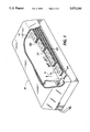
- FIG. 1 is a fragmentary perspective view of a multicolor pagewidth type thermal ink jet printer having four pagewidth printbars.
- FIG. 2 is a schematic elevational view of a printhead element.
- FIG. 3 is a schematic plan view of a silicon wafer having individual elements.
- FIG. 4 is a schematic plan view of a heater element.
- FIG. 5 is a schematic plan view of a channel element.
- FIG. 6 is a schematic fragmentary elevational view of a channel element wafer and heater element wafer having dice cuts before mating.
- FIG. 7 is a schematic fragmentary elevational view of a channel element wafer bonded to a heater element wafer having dice cuts and back cuts.
- FIG. 8 is a schematic plan view of a channel element having etch troughs.
- FIG. 9 is a schematic elevational view of a printhead element having a defined space between the channel element and printhead element.
- FIG. 10 is a schematic elevational view of the posterior side of a printhead array made of individual printhead elements and a supporting substrate.
- FIG. 1 is a fragmentary perspective view of a pagewidth type, multicolor, thermal ink jet printer 10.
- a pagewidth monochrome printer has a stationary printbar 12A having a length equal to or greater than the length of a sheet of paper 14.
- a multicolor pagewidth printer has four stationary printbars 12A, 12B, 12C, 12D stacked one over the other, with the side nozzles of each printbar in alignment with each other.
- a frame 15 supports the stationary printbars 12A through 12D in spaced relationship with the sheet of paper 14 for printing thereon.
- the paper 14 is continually moved past the pagewidth printbars in the direction of arrow 16, a direction normal to the printbar length and at a constant speed during the printing process.
- U.S. Pat. Nos. 4,463,359 to Ayata et al. and 4,829,324 to Drake et al. for examples of pagewidth printing.
- the stationary printbar 12 can be made of any number of individual printheads 18. For instance, a full page width printhead array printing across the short edge of a sheet of 81/2" ⁇ 11" paper could consist of approximately 10 or more individual printheads 18 depending on the number of spots per inch. Likewise, if paper is being printed along the long edge of a sheet of 81/2" ⁇ 11" paper, then the printbar 12 might consist of 15 or more individual printheads 18.
- the number of individual printheads 18 comprising the printbar 12A not only depends on the length of the sheet of paper being printed upon but also depends upon the number of channel openings or nozzles in each of the individual printheads 18.
- one of the individual printheads 18 can have anywhere from 50 to 300 or more individual nozzles.
- the printhead element 18 includes a plurality of nozzles 20 arranged in side by side relationship along a front face 22 of a channel element or upper substrate 24.
- the upper substrate 24 of each individual printhead 18 also includes one or more fill holes 26 which allow for ink to fill the nozzles 20 through capillary action for later deposition upon the sheet of paper 14.
- the channel element 24 includes a butting edge 25 which intersects the front face 22. In a pagewidth array, the butting edge 25 contacts the channel element butting edge of an adjacent printhead element 18. While the butting edges have a surface area, the term "butting edge" is used to distinguish over other surfaces described herein.
- each of the channel elements 24 Located below each of the channel elements 24 is a lower electrical substrate or heating element 28 having a second front face 27 intersecting a butting edge 29.
- the butting edge 29 contacts the butting edge of the heater element of an adjacent printhead element 18.
- the heating element 28 includes electrical circuitry for causing ink to be expelled from each of the individual nozzles 20. Any known method may be used to fabricate the individual printhead elements 18. Examples are U.S. Pat. No. 32,572 to Hawkins et al., U.S. Pat. No. 4,774,530 to Hawkins and U.S. Pat. No. 5,000,811 to Campanelli, all incorporated herein by reference.
- FIG. 3 illustrates a single silicon wafer 30 including a plurality of individual elements 31, which are either channel elements 24 or heater elements 28. One or both sides of the silicon wafer is polished depending on whether heater elements or channel elements are being formed.
- Each of the individual elements 31 located on the wafer 30 is delineated by vertical separation lines 33A and horizontal separation lines 33B to define the outer edges or boundaries of each of the individual elements 31. Dicing cuts are made at the separation lines 33 to separate one element 31 from an adjacent element 31.
- a single heater element 28 is illustrated in FIG. 4.
- a plurality of heaters or resistors 32, drivers 34, addressing logic 36 and the electrodes 38 are patterned on the polished surface of a single side polished (100) silicon wafer.
- the silicon wafer can have up to 256 individual heating elements 28 or more depending on the diameter of the silicon wafer being patterned. Also shown are the respective locations of the addressing logic 36, the drivers 34 and the heaters 32 on the heating element 28.
- the individual heaters 32 are patterned on the silicon substrate in side by side relationship so that each individual heater will be strategically associated with a corresponding nozzle when the heater element 28 is mated to the channel element 24.
- Each of the individual heaters 32 is driven by a portion of the electronic circuitry consisting of semiconductor drivers 34 which are, in turn, driven by logic circuitry 36.
- the logic circuitry 36, the drivers 34 and the heaters 32 are all formed on the silicon chip by known large scale integrated circuit techniques.
- the logic circuitry 36 is, in turn, connected to electrode terminals 38 which receive signals through wire bonds connected to electrodes 38.
- Control circuitry connected to the electrodes 38 selects which of the individual nozzles 20 of the printhead element 18 expel ink.
- the logic circuitry and driving circuitry which is used to pulse the individual heaters 36 is shown in U.S. patent application Ser. No. 07/971,873 assigned to the present assignee and herein completely incorporated by reference.
- a thick film insulating layer 39 (see FIG. 2) such as Vacrel®, Riston®, Probimer®, or polyimide is deposited on top of the circuitry on the heater element 28.
- the thick film insulating layer 39 is a passivation layer sandwiched between the upper and lower substrates. MOS fabrication techniques are used for multilayer passivation of the logic circuitry and the drivers which will also protect the circuitry from mobile ions and ink similar to the methods disclosed in U.S. Pat. No. 5,010,355 to Hawkins, et al., the pertinent portions of which are herein incorporated by reference.
- a silicon channel wafer includes a number of channel elements 24 which are formed on the surface of the silicon wafer.
- One of the individual channel elements 24 is shown in an enlarged view in FIG. 5.
- the channel wafer used to produce a plurality of channel elements 24 for individual or large array printheads is a two sided polished (100) silicon wafer. After the wafer is chemically cleaned, a silicon nitride layer, not shown, is deposited on both sides.
- the channel wafer is photolithographically patterned to form a plurality of channel grooves 42, and one or more fill holes 26.
- a potassium hydroxide (KOH) anisotropic edge is used to etch the channels 42 and fill holes 26:
- KOH potassium hydroxide
- the ⁇ 111 ⁇ planes of the (100) wafer make an angle of 54.7° with the surface of the wafer.
- Anisotropic etching is described in U.S. Pat. No. 4,957,592 to O'Neill, the relevant portions of which are incorporated by reference.
- Individual printhead elements are made by aligning and joining a heater wafer to a channel wafer. Because each of the individual channel elements 24 and heating elements 28 are patterned on large silicon wafers, each individual element must be separated from its adjoining element on the respective silicon wafer to form a printhead array. For instance, the separation of individual heating elements 28 from the silicon wafer can be accomplished by any number of known dicing operations made along parallel separation lines 44 and 46 (see FIG. 4) which correspond respectively to vertical separation line 33A and horizontal separation line 33B of FIG. 3. This fabrication process, likewise requires that parallel milling or dicing cuts be made at lines 48 and 50 of the channel element 24 of FIG. 5. Dicing along the line 50A creates the nozzles 20.
- FIG. 6 illustrates the heater wafer and the channel wafer before mating, each having respective pre-dicing cuts 51 and 52 which have been made to the mating surfaces of each of the wafers.
- Pre-dicing cuts have a depth of less than the thickness of the wafer.
- FIG. 7 illustrates a further step in the process in which individual printheads are manufactured by placing a back cut 54 and a back cut 56 sufficiently deep to meet the pre-dicing cuts 51 and 52. A single cut through the pre-dicing cuts is also possible. Once cut, individual printheads 18 are separated from the entire two-wafer structure consisting of the channel wafer and the heater wafer.
- the layer of adhesive or epoxy is placed on the channel wafer before it is mated with the heater wafer.
- This layer of epoxy has a thickness of approximately 1 micron thick.
- the epoxy is deposited over the flat unetched surfaces of each of channel elements 24 as shown in FIG. 5.
- the epoxy covers the flat surface areas between adjacent channels 42, between the channels 42 and the fill holes 26, and a large flat surface 60 between the fill holes 26 and the parallel dicing cut 50B.
- Flat surface 60 typically remains unetched. Consequently, surface 60 contains a relatively large amount of epoxy with respect to the other areas of the channel element 24.
- excess epoxy is forced or squeezed by the pressure of mating from between the elements in a mass or blob of excess epoxy 61 as illustrated in FIG. 7. It should be noted that the epoxy does not typically flow out the sides adjacent to the channels 42 or the fill holes 26 since the surface areas containing epoxy in these regions is relatively small but epoxy is likely to flow out adjacent to the flat surface 60. This epoxy flows onto the precision diced edges of the buttable printhead elements 18 thereby causing the butting edges to be nonsmooth. Excess epoxy 61 is also shown in FIG. 2.
- a first overflow trough 64 and a second overflow trough 66 are formed on the surface 60 of the channel element 24 as illustrated in FIG. 8.
- the first overflow trough 64 and the second overflow trough 66 are located posterior to the fill holes 26.
- Each of the overflow troughs 64 and 66 are approximately 50 microns wide and actually straddle the separation lines 48.
- Each etch trough is formed by etching in the same fashion as the channels 42.
- the large surface area 60 is a critical area because this largely unetched region of the channel element 24 acquires a relatively large amount of epoxy during manufacture and consequently tends to produce excess epoxy which squeezes out at the butting edges once the channel element 24 is mated to the heater element 28.
- the parallel separation line 50B as illustrated in FIG. 8 cuts across each of the first etch trough 64 and the second etch trough 66 thereby exposing an open end of each of the etch troughs.
- the heater wafer and the channel wafer having etch troughs are aligned, prediced, mated, and diced to form the individual printhead elements 18 as illustrated in FIG. 9.
- the printhead element 18 includes a space or adhesive-receiving aperture 68 formed between the channel element 24 and the heater element 28.
- the first butting edge 25 and the second butting edge 29 still form an essentially flat edge for butting with an adjacent printhead element 18.
- the space 68 now receives adhesive and prevents adhesive from being squeezed onto either the first butting edge 25 or the second butting edge 29.
- FIG. 10 illustrates a posterior view of a large array printbar 70 made of a plurality of the individual printhead elements 18.
- the individual printhead elements 18 are mated and aligned with other printhead elements 18 to form the large array printbar 70.
- the printhead elements 18 are placed on a thermo-setting epoxy 72 applied upon a supporting substrate 74.
- a UV adhesive droplet 76 is placed at either end of the printhead array.
- the space 68 created by the etch trough receives any excess epoxy 61 which would otherwise flow from between the channel element 24 and heater element 28.
- the excess epoxy is still squeezed out from between the channel element and the heater element, but due to the space 68, none of the epoxy flows over either the butting edge 25 or the butting edge 29. Consequently, by forming a space between the channel element 24 and the heater element 28 just inside where the heater element butting edge and channel element butting edge meet, problems resulting from epoxy squeeze-out are eliminated or substantially reduced.
- the etch trough could be formed so that, in cross-section, the apex of the triangle is bisected by the predice cut.
- a single etch trough could be formed at the boundaries between adjacent channel elements, so that a single etch trough could function, when bisected by the pre-dicing and dice cuts, as an adhesive-receiving feature for two channel elements. Accordingly, it is intended to embrace all such alternatives, modifications and variations that fall within the spirit and broad scope of the appended claims.
Abstract
Description
Claims (20)
Priority Applications (1)
| Application Number | Priority Date | Filing Date | Title |
|---|---|---|---|
| US08/280,973 US5572244A (en) | 1994-07-27 | 1994-07-27 | Adhesive-free edge butting for printhead elements |
Applications Claiming Priority (1)
| Application Number | Priority Date | Filing Date | Title |
|---|---|---|---|
| US08/280,973 US5572244A (en) | 1994-07-27 | 1994-07-27 | Adhesive-free edge butting for printhead elements |
Publications (1)
| Publication Number | Publication Date |
|---|---|
| US5572244A true US5572244A (en) | 1996-11-05 |
Family
ID=23075427
Family Applications (1)
| Application Number | Title | Priority Date | Filing Date |
|---|---|---|---|
| US08/280,973 Expired - Lifetime US5572244A (en) | 1994-07-27 | 1994-07-27 | Adhesive-free edge butting for printhead elements |
Country Status (1)
| Country | Link |
|---|---|
| US (1) | US5572244A (en) |
Cited By (21)
| Publication number | Priority date | Publication date | Assignee | Title |
|---|---|---|---|---|
| US5952988A (en) * | 1996-11-12 | 1999-09-14 | University Technology Corp | Display having gradient response pixels |
| US6076244A (en) * | 1997-11-17 | 2000-06-20 | Seiko Epson Corporation | Heat treatment method of actuators for an ink jet printer head and method for manufacturing an ink jet printer head |
| US6089693A (en) * | 1998-01-08 | 2000-07-18 | Xerox Corporation | Pagewidth ink jet printer including multiple pass defective nozzle correction |
| US6164762A (en) * | 1998-06-19 | 2000-12-26 | Lexmark International, Inc. | Heater chip module and process for making same |
| US6209993B1 (en) * | 1998-05-29 | 2001-04-03 | Industrial Technology Research Institute | Structure and fabricating method for ink-jet printhead chip |
| US6234605B1 (en) | 1998-01-08 | 2001-05-22 | Xerox Corporation | Multiple resolution pagewidth ink jet printer including a positionable pagewidth printbear |
| EP1136269A2 (en) * | 2000-03-21 | 2001-09-26 | Nec Corporation | Ink jet head having a plurality of units and its manufacturing method |
| US6382769B1 (en) * | 1997-07-15 | 2002-05-07 | Silverbrook Research Pty Ltd | Method of tab alignment in an integrated circuit type device |
| US6565760B2 (en) | 2000-02-28 | 2003-05-20 | Hewlett-Packard Development Company, L.P. | Glass-fiber thermal inkjet print head |
| US20040028445A1 (en) * | 2000-09-15 | 2004-02-12 | Kia Silverbrook | Elongate printhead assembly including multiple fluid supply galleries |
| US20040080564A1 (en) * | 2002-10-24 | 2004-04-29 | Maher Edward P. | Printing device and method |
| US6869162B2 (en) | 2003-03-27 | 2005-03-22 | Hewlett-Packard Development Company, L.P. | Printing device and method for servicing same |
| US20050157053A1 (en) * | 2004-01-21 | 2005-07-21 | Silverbrook Research Pty Ltd | Method for facilitating maintenance of an inkjet printer having a pagewidth printhead |
| US20050162472A1 (en) * | 1999-12-09 | 2005-07-28 | Kia Silverbrook | Printhead module |
| US20060055731A1 (en) * | 2004-09-13 | 2006-03-16 | Canon Kabushiki Kaisha | Ink jet head, ink jet printer and method for manufacturing ink jet head |
| US20070109356A1 (en) * | 1999-12-09 | 2007-05-17 | Silverbrook Research Pty Ltd | Modular printhead assembly with reservoir mounted printhead modules |
| US20070296795A1 (en) * | 2006-06-26 | 2007-12-27 | Dante Frati | Process for printing surfaces of wood-based flat elements |
| US20100156992A1 (en) * | 2008-12-18 | 2010-06-24 | Yonglin Xie | Buttable printhead module and pagewide printhead |
| US20110088838A1 (en) * | 2009-10-16 | 2011-04-21 | Apple Inc. | Self fixturing assembly techniques |
| US8079683B2 (en) | 2004-01-21 | 2011-12-20 | Silverbrook Research Pty Ltd | Inkjet printer cradle with shaped recess for receiving a printer cartridge |
| US8439497B2 (en) | 2004-01-21 | 2013-05-14 | Zamtec Ltd | Image processing apparatus with nested printer and scanner |
Citations (9)
| Publication number | Priority date | Publication date | Assignee | Title |
|---|---|---|---|---|
| US4678529A (en) * | 1986-07-02 | 1987-07-07 | Xerox Corporation | Selective application of adhesive and bonding process for ink jet printheads |
| USRE32572E (en) * | 1985-04-03 | 1988-01-05 | Xerox Corporation | Thermal ink jet printhead and process therefor |
| US4774530A (en) * | 1987-11-02 | 1988-09-27 | Xerox Corporation | Ink jet printhead |
| US4829324A (en) * | 1987-12-23 | 1989-05-09 | Xerox Corporation | Large array thermal ink jet printhead |
| US5000811A (en) * | 1989-11-22 | 1991-03-19 | Xerox Corporation | Precision buttable subunits via dicing |
| US5160403A (en) * | 1991-08-09 | 1992-11-03 | Xerox Corporation | Precision diced aligning surfaces for devices such as ink jet printheads |
| JPH0511200A (en) * | 1991-07-02 | 1993-01-19 | Canon Inc | Scanning optical device |
| US5198054A (en) * | 1991-08-12 | 1993-03-30 | Xerox Corporation | Method of making compensated collinear reading or writing bar arrays assembled from subunits |
| US5221397A (en) * | 1992-11-02 | 1993-06-22 | Xerox Corporation | Fabrication of reading or writing bar arrays assembled from subunits |
-
1994
- 1994-07-27 US US08/280,973 patent/US5572244A/en not_active Expired - Lifetime
Patent Citations (9)
| Publication number | Priority date | Publication date | Assignee | Title |
|---|---|---|---|---|
| USRE32572E (en) * | 1985-04-03 | 1988-01-05 | Xerox Corporation | Thermal ink jet printhead and process therefor |
| US4678529A (en) * | 1986-07-02 | 1987-07-07 | Xerox Corporation | Selective application of adhesive and bonding process for ink jet printheads |
| US4774530A (en) * | 1987-11-02 | 1988-09-27 | Xerox Corporation | Ink jet printhead |
| US4829324A (en) * | 1987-12-23 | 1989-05-09 | Xerox Corporation | Large array thermal ink jet printhead |
| US5000811A (en) * | 1989-11-22 | 1991-03-19 | Xerox Corporation | Precision buttable subunits via dicing |
| JPH0511200A (en) * | 1991-07-02 | 1993-01-19 | Canon Inc | Scanning optical device |
| US5160403A (en) * | 1991-08-09 | 1992-11-03 | Xerox Corporation | Precision diced aligning surfaces for devices such as ink jet printheads |
| US5198054A (en) * | 1991-08-12 | 1993-03-30 | Xerox Corporation | Method of making compensated collinear reading or writing bar arrays assembled from subunits |
| US5221397A (en) * | 1992-11-02 | 1993-06-22 | Xerox Corporation | Fabrication of reading or writing bar arrays assembled from subunits |
Cited By (55)
| Publication number | Priority date | Publication date | Assignee | Title |
|---|---|---|---|---|
| US5952988A (en) * | 1996-11-12 | 1999-09-14 | University Technology Corp | Display having gradient response pixels |
| US6382769B1 (en) * | 1997-07-15 | 2002-05-07 | Silverbrook Research Pty Ltd | Method of tab alignment in an integrated circuit type device |
| US6076244A (en) * | 1997-11-17 | 2000-06-20 | Seiko Epson Corporation | Heat treatment method of actuators for an ink jet printer head and method for manufacturing an ink jet printer head |
| US6234605B1 (en) | 1998-01-08 | 2001-05-22 | Xerox Corporation | Multiple resolution pagewidth ink jet printer including a positionable pagewidth printbear |
| US6089693A (en) * | 1998-01-08 | 2000-07-18 | Xerox Corporation | Pagewidth ink jet printer including multiple pass defective nozzle correction |
| US6209993B1 (en) * | 1998-05-29 | 2001-04-03 | Industrial Technology Research Institute | Structure and fabricating method for ink-jet printhead chip |
| US6164762A (en) * | 1998-06-19 | 2000-12-26 | Lexmark International, Inc. | Heater chip module and process for making same |
| US20050162472A1 (en) * | 1999-12-09 | 2005-07-28 | Kia Silverbrook | Printhead module |
| US7677698B2 (en) | 1999-12-09 | 2010-03-16 | Silverbrook Research Pty Ltd | Modular printhead assembly with reservoir mounted printhead modules |
| US20100002056A1 (en) * | 1999-12-09 | 2010-01-07 | Silverbrook Research Pty Ltd | Modular printhead assembly having reservoir mounted printhead modules |
| US20070109356A1 (en) * | 1999-12-09 | 2007-05-17 | Silverbrook Research Pty Ltd | Modular printhead assembly with reservoir mounted printhead modules |
| US7182441B2 (en) * | 1999-12-09 | 2007-02-27 | Silverbrook Research Pty Ltd | Printhead module |
| US6565760B2 (en) | 2000-02-28 | 2003-05-20 | Hewlett-Packard Development Company, L.P. | Glass-fiber thermal inkjet print head |
| EP1136269A2 (en) * | 2000-03-21 | 2001-09-26 | Nec Corporation | Ink jet head having a plurality of units and its manufacturing method |
| EP1136269A3 (en) * | 2000-03-21 | 2001-10-04 | Nec Corporation | Ink jet head having a plurality of units and its manufacturing method |
| US6502921B2 (en) | 2000-03-21 | 2003-01-07 | Fuji Xerox Co., Ltd. | Ink jet head having a plurality of units and its manufacturing method |
| US7556369B2 (en) | 2000-09-15 | 2009-07-07 | Silverbrook Research Pty Ltd | Printer with set spacing between a print engine and an exit roller assembly |
| US7901067B2 (en) | 2000-09-15 | 2011-03-08 | Silverbrook Research Pty Ltd. | Print media loading mechanism having displaceable endless belts |
| US20050157135A1 (en) * | 2000-09-15 | 2005-07-21 | Kia Silverbrook | Print engine |
| US8113650B2 (en) | 2000-09-15 | 2012-02-14 | Silverbrook Resesarch Pty Ltd | Printer having arcuate printhead |
| US6869172B2 (en) * | 2000-09-15 | 2005-03-22 | Silverbrook Research Pty Ltd | Printhead assembly having two sets of fluid inlets |
| US6966636B2 (en) * | 2000-09-15 | 2005-11-22 | Silverbrook Research Pty Ltd | Elongate printhead assembly including multiple fluid supply galleries |
| US20050275702A1 (en) * | 2000-09-15 | 2005-12-15 | Silverbrook Research Pty Ltd | Printer for duplex printing with multiple printhead modules |
| US7946702B2 (en) | 2000-09-15 | 2011-05-24 | Silverbrook Research Pty Ltd | Printer incorporating partially arcuate printhead |
| US20050140756A1 (en) * | 2000-09-15 | 2005-06-30 | Kia Silverbrook | Printhead assembly having modular ink distribution |
| US7771019B2 (en) | 2000-09-15 | 2010-08-10 | Silverbrook Research Pty Ltd | Stackable printer module for effecting double-sided printing |
| US7222940B2 (en) | 2000-09-15 | 2007-05-29 | Silverbrook Research Pty Ltd | Print engine |
| US7222941B2 (en) | 2000-09-15 | 2007-05-29 | Silverbrook Research Pty Ltd | Printer for duplex printing with multiple printhead modules |
| US7284822B2 (en) | 2000-09-15 | 2007-10-23 | Silverbrook Research Pty Ltd | Printhead assembly having modular ink distribution |
| US20040028445A1 (en) * | 2000-09-15 | 2004-02-12 | Kia Silverbrook | Elongate printhead assembly including multiple fluid supply galleries |
| US20080012902A1 (en) * | 2000-09-15 | 2008-01-17 | Silverbrook Research Pty Ltd | Stackable printer module for effecting double-sided printing |
| US7364286B2 (en) | 2000-09-15 | 2008-04-29 | Silverbrook Research Pty Ltd | Print engine incorporating a quartet of printhead modules arranged in pairs |
| US20080159801A1 (en) * | 2000-09-15 | 2008-07-03 | Silverbrook Research Pty Ltd | Print media loading mechanism having displaceable endless belts |
| US20080166171A1 (en) * | 2000-09-15 | 2008-07-10 | Silverbrook Research Pty Ltd | Printer with set spacing between a print engine and an exit roller assembly |
| US20040027429A1 (en) * | 2000-09-15 | 2004-02-12 | Kia Silverbrook | Printhead assembly having two sets of fluid inlets |
| US20090237481A1 (en) * | 2000-09-15 | 2009-09-24 | Silverbrook Research Pty Ltd | Printer Incorporating Partially Arcuate Printhead |
| US7472989B2 (en) | 2000-09-15 | 2009-01-06 | Silverbrook Research Pty Ltd | Print media loading mechanism having displaceable endless belts |
| US20040080564A1 (en) * | 2002-10-24 | 2004-04-29 | Maher Edward P. | Printing device and method |
| US6814421B2 (en) | 2002-10-24 | 2004-11-09 | Hewlett-Packard Development Company, L.P. | Printing device and method |
| US6869162B2 (en) | 2003-03-27 | 2005-03-22 | Hewlett-Packard Development Company, L.P. | Printing device and method for servicing same |
| US8079683B2 (en) | 2004-01-21 | 2011-12-20 | Silverbrook Research Pty Ltd | Inkjet printer cradle with shaped recess for receiving a printer cartridge |
| US7425050B2 (en) * | 2004-01-21 | 2008-09-16 | Silverbrook Research Pty Ltd | Method for facilitating maintenance of an inkjet printer having a pagewidth printhead |
| US8439497B2 (en) | 2004-01-21 | 2013-05-14 | Zamtec Ltd | Image processing apparatus with nested printer and scanner |
| US20080291250A1 (en) * | 2004-01-21 | 2008-11-27 | Silverbrook Research Pty Ltd | Printer cartridge for a pagewidth printer having a refill port and a controller board |
| US20050157053A1 (en) * | 2004-01-21 | 2005-07-21 | Silverbrook Research Pty Ltd | Method for facilitating maintenance of an inkjet printer having a pagewidth printhead |
| US7410241B2 (en) * | 2004-09-13 | 2008-08-12 | Canon Kabushiki Kaisha | Ink jet head, ink jet printer and method for manufacturing ink jet head |
| US20060055731A1 (en) * | 2004-09-13 | 2006-03-16 | Canon Kabushiki Kaisha | Ink jet head, ink jet printer and method for manufacturing ink jet head |
| US8960828B2 (en) | 2006-06-26 | 2015-02-24 | Dante Frati | Process for printing wood-based flat elements and production line |
| US9340033B2 (en) | 2006-06-26 | 2016-05-17 | Dante Frati | Process for printing wood-based flat elements and production line |
| US20070296795A1 (en) * | 2006-06-26 | 2007-12-27 | Dante Frati | Process for printing surfaces of wood-based flat elements |
| US8328303B2 (en) | 2006-06-26 | 2012-12-11 | Dante Frati | Process for printing surfaces of wood-based flat elements |
| US8118405B2 (en) | 2008-12-18 | 2012-02-21 | Eastman Kodak Company | Buttable printhead module and pagewide printhead |
| US20100156992A1 (en) * | 2008-12-18 | 2010-06-24 | Yonglin Xie | Buttable printhead module and pagewide printhead |
| US8333862B2 (en) * | 2009-10-16 | 2012-12-18 | Apple Inc. | Self fixturing assembly techniques |
| US20110088838A1 (en) * | 2009-10-16 | 2011-04-21 | Apple Inc. | Self fixturing assembly techniques |
Similar Documents
| Publication | Publication Date | Title |
|---|---|---|
| US5572244A (en) | Adhesive-free edge butting for printhead elements | |
| US4829324A (en) | Large array thermal ink jet printhead | |
| US5755024A (en) | Printhead element butting | |
| EP0430692B1 (en) | Method for making printheads | |
| US5041190A (en) | Method of fabricating channel plates and ink jet printheads containing channel plates | |
| US4851371A (en) | Fabricating process for large array semiconductive devices | |
| JP2957003B2 (en) | How to make a precise joining edge for printhead chips | |
| US4639748A (en) | Ink jet printhead with integral ink filter | |
| US7731861B2 (en) | Liquid drop discharge head and manufacture method thereof, micro device, ink-jet head, ink cartridge, and ink-jet printing device | |
| JPS61230954A (en) | Manufacture of printing head for heat-sensitive ink jet | |
| JP2001071503A (en) | Printer having ink jet print head, manufacture thereof and method for printing | |
| JP3007395B2 (en) | Thermal inkjet printer system | |
| JPH07205423A (en) | Ink-jet print head | |
| US5410340A (en) | Off center heaters for thermal ink jet printheads | |
| EP0754554B1 (en) | Method of fabricating an orifice plate | |
| JP3108930B2 (en) | Ink jet head and method of manufacturing the same | |
| JPH0796605A (en) | Ink jet type recording head | |
| EP0757940B1 (en) | A liquid jet recording head, and a manufacturing method thereof, as well as a liquid jet recording apparatus with said liquid jet recording head mounted thereon | |
| JP4326772B2 (en) | Droplet discharge head, ink cartridge, and ink jet recording apparatus | |
| JP3564864B2 (en) | Method of manufacturing inkjet head | |
| JP2004167951A (en) | Liquid jet head, manufacturing method for the same, ink cartridge, and inkjet recorder | |
| JP3255788B2 (en) | Ink jet recording head and method of manufacturing ink jet recording head | |
| JPH0957966A (en) | Ink jet head and ink jet recording apparatus | |
| JP2002096473A (en) | Liquid drop discharge head | |
| JPH07205426A (en) | Ink jet print head and production of thermal ink jet print head |
Legal Events
| Date | Code | Title | Description |
|---|---|---|---|
| AS | Assignment |
Owner name: XEROX CORPORATION, CONNECTICUT Free format text: ASSIGNMENT OF ASSIGNORS INTEREST;ASSIGNORS:DRAKE, DONALD J.;NGUYEN, HUNG C.;REEL/FRAME:007098/0656 Effective date: 19940722 |
|
| STCF | Information on status: patent grant |
Free format text: PATENTED CASE |
|
| FPAY | Fee payment |
Year of fee payment: 4 |
|
| AS | Assignment |
Owner name: BANK ONE, NA, AS ADMINISTRATIVE AGENT, ILLINOIS Free format text: SECURITY INTEREST;ASSIGNOR:XEROX CORPORATION;REEL/FRAME:013153/0001 Effective date: 20020621 |
|
| AS | Assignment |
Owner name: JPMORGAN CHASE BANK, AS COLLATERAL AGENT, TEXAS Free format text: SECURITY AGREEMENT;ASSIGNOR:XEROX CORPORATION;REEL/FRAME:015134/0476 Effective date: 20030625 Owner name: JPMORGAN CHASE BANK, AS COLLATERAL AGENT,TEXAS Free format text: SECURITY AGREEMENT;ASSIGNOR:XEROX CORPORATION;REEL/FRAME:015134/0476 Effective date: 20030625 |
|
| FPAY | Fee payment |
Year of fee payment: 8 |
|
| FPAY | Fee payment |
Year of fee payment: 12 |
|
| AS | Assignment |
Owner name: XEROX CORPORATION, CONNECTICUT Free format text: RELEASE BY SECURED PARTY;ASSIGNOR:JPMORGAN CHASE BANK, N.A. AS SUCCESSOR-IN-INTEREST ADMINISTRATIVE AGENT AND COLLATERAL AGENT TO JPMORGAN CHASE BANK;REEL/FRAME:066728/0193 Effective date: 20220822 |