US5567362A - Identity card and a method and apparatus for producing it - Google Patents
Identity card and a method and apparatus for producing it Download PDFInfo
- Publication number
- US5567362A US5567362A US08/288,041 US28804194A US5567362A US 5567362 A US5567362 A US 5567362A US 28804194 A US28804194 A US 28804194A US 5567362 A US5567362 A US 5567362A
- Authority
- US
- United States
- Prior art keywords
- mold
- resin portion
- card
- layer
- card body
- Prior art date
- Legal status (The legal status is an assumption and is not a legal conclusion. Google has not performed a legal analysis and makes no representation as to the accuracy of the status listed.)
- Expired - Fee Related
Links
Images


Classifications
-
- B—PERFORMING OPERATIONS; TRANSPORTING
- B29—WORKING OF PLASTICS; WORKING OF SUBSTANCES IN A PLASTIC STATE IN GENERAL
- B29C—SHAPING OR JOINING OF PLASTICS; SHAPING OF MATERIAL IN A PLASTIC STATE, NOT OTHERWISE PROVIDED FOR; AFTER-TREATMENT OF THE SHAPED PRODUCTS, e.g. REPAIRING
- B29C45/00—Injection moulding, i.e. forcing the required volume of moulding material through a nozzle into a closed mould; Apparatus therefor
- B29C45/16—Making multilayered or multicoloured articles
-
- B—PERFORMING OPERATIONS; TRANSPORTING
- B42—BOOKBINDING; ALBUMS; FILES; SPECIAL PRINTED MATTER
- B42D—BOOKS; BOOK COVERS; LOOSE LEAVES; PRINTED MATTER CHARACTERISED BY IDENTIFICATION OR SECURITY FEATURES; PRINTED MATTER OF SPECIAL FORMAT OR STYLE NOT OTHERWISE PROVIDED FOR; DEVICES FOR USE THEREWITH AND NOT OTHERWISE PROVIDED FOR; MOVABLE-STRIP WRITING OR READING APPARATUS
- B42D25/00—Information-bearing cards or sheet-like structures characterised by identification or security features; Manufacture thereof
- B42D25/20—Information-bearing cards or sheet-like structures characterised by identification or security features; Manufacture thereof characterised by a particular use or purpose
- B42D25/23—Identity cards
-
- B—PERFORMING OPERATIONS; TRANSPORTING
- B42—BOOKBINDING; ALBUMS; FILES; SPECIAL PRINTED MATTER
- B42D—BOOKS; BOOK COVERS; LOOSE LEAVES; PRINTED MATTER CHARACTERISED BY IDENTIFICATION OR SECURITY FEATURES; PRINTED MATTER OF SPECIAL FORMAT OR STYLE NOT OTHERWISE PROVIDED FOR; DEVICES FOR USE THEREWITH AND NOT OTHERWISE PROVIDED FOR; MOVABLE-STRIP WRITING OR READING APPARATUS
- B42D25/00—Information-bearing cards or sheet-like structures characterised by identification or security features; Manufacture thereof
- B42D25/30—Identification or security features, e.g. for preventing forgery
- B42D25/324—Reliefs
-
- B—PERFORMING OPERATIONS; TRANSPORTING
- B42—BOOKBINDING; ALBUMS; FILES; SPECIAL PRINTED MATTER
- B42D—BOOKS; BOOK COVERS; LOOSE LEAVES; PRINTED MATTER CHARACTERISED BY IDENTIFICATION OR SECURITY FEATURES; PRINTED MATTER OF SPECIAL FORMAT OR STYLE NOT OTHERWISE PROVIDED FOR; DEVICES FOR USE THEREWITH AND NOT OTHERWISE PROVIDED FOR; MOVABLE-STRIP WRITING OR READING APPARATUS
- B42D25/00—Information-bearing cards or sheet-like structures characterised by identification or security features; Manufacture thereof
- B42D25/30—Identification or security features, e.g. for preventing forgery
- B42D25/328—Diffraction gratings; Holograms
-
- B—PERFORMING OPERATIONS; TRANSPORTING
- B42—BOOKBINDING; ALBUMS; FILES; SPECIAL PRINTED MATTER
- B42D—BOOKS; BOOK COVERS; LOOSE LEAVES; PRINTED MATTER CHARACTERISED BY IDENTIFICATION OR SECURITY FEATURES; PRINTED MATTER OF SPECIAL FORMAT OR STYLE NOT OTHERWISE PROVIDED FOR; DEVICES FOR USE THEREWITH AND NOT OTHERWISE PROVIDED FOR; MOVABLE-STRIP WRITING OR READING APPARATUS
- B42D25/00—Information-bearing cards or sheet-like structures characterised by identification or security features; Manufacture thereof
- B42D25/40—Manufacture
-
- G—PHYSICS
- G06—COMPUTING; CALCULATING OR COUNTING
- G06K—GRAPHICAL DATA READING; PRESENTATION OF DATA; RECORD CARRIERS; HANDLING RECORD CARRIERS
- G06K19/00—Record carriers for use with machines and with at least a part designed to carry digital markings
- G06K19/04—Record carriers for use with machines and with at least a part designed to carry digital markings characterised by the shape
- G06K19/041—Constructional details
-
- G—PHYSICS
- G06—COMPUTING; CALCULATING OR COUNTING
- G06K—GRAPHICAL DATA READING; PRESENTATION OF DATA; RECORD CARRIERS; HANDLING RECORD CARRIERS
- G06K19/00—Record carriers for use with machines and with at least a part designed to carry digital markings
- G06K19/06—Record carriers for use with machines and with at least a part designed to carry digital markings characterised by the kind of the digital marking, e.g. shape, nature, code
- G06K19/067—Record carriers with conductive marks, printed circuits or semiconductor circuit elements, e.g. credit or identity cards also with resonating or responding marks without active components
- G06K19/07—Record carriers with conductive marks, printed circuits or semiconductor circuit elements, e.g. credit or identity cards also with resonating or responding marks without active components with integrated circuit chips
- G06K19/077—Constructional details, e.g. mounting of circuits in the carrier
- G06K19/0772—Physical layout of the record carrier
- G06K19/07724—Physical layout of the record carrier the record carrier being at least partially made by a molding process
-
- G—PHYSICS
- G06—COMPUTING; CALCULATING OR COUNTING
- G06K—GRAPHICAL DATA READING; PRESENTATION OF DATA; RECORD CARRIERS; HANDLING RECORD CARRIERS
- G06K19/00—Record carriers for use with machines and with at least a part designed to carry digital markings
- G06K19/06—Record carriers for use with machines and with at least a part designed to carry digital markings characterised by the kind of the digital marking, e.g. shape, nature, code
- G06K19/067—Record carriers with conductive marks, printed circuits or semiconductor circuit elements, e.g. credit or identity cards also with resonating or responding marks without active components
- G06K19/07—Record carriers with conductive marks, printed circuits or semiconductor circuit elements, e.g. credit or identity cards also with resonating or responding marks without active components with integrated circuit chips
- G06K19/077—Constructional details, e.g. mounting of circuits in the carrier
- G06K19/07745—Mounting details of integrated circuit chips
-
- B—PERFORMING OPERATIONS; TRANSPORTING
- B29—WORKING OF PLASTICS; WORKING OF SUBSTANCES IN A PLASTIC STATE IN GENERAL
- B29C—SHAPING OR JOINING OF PLASTICS; SHAPING OF MATERIAL IN A PLASTIC STATE, NOT OTHERWISE PROVIDED FOR; AFTER-TREATMENT OF THE SHAPED PRODUCTS, e.g. REPAIRING
- B29C45/00—Injection moulding, i.e. forcing the required volume of moulding material through a nozzle into a closed mould; Apparatus therefor
- B29C45/16—Making multilayered or multicoloured articles
- B29C2045/1681—Making multilayered or multicoloured articles one layer penetrating at one or more areas through another layer
-
- B—PERFORMING OPERATIONS; TRANSPORTING
- B29—WORKING OF PLASTICS; WORKING OF SUBSTANCES IN A PLASTIC STATE IN GENERAL
- B29L—INDEXING SCHEME ASSOCIATED WITH SUBCLASS B29C, RELATING TO PARTICULAR ARTICLES
- B29L2017/00—Carriers for sound or information
- B29L2017/006—Memory cards, chip cards
-
- B—PERFORMING OPERATIONS; TRANSPORTING
- B29—WORKING OF PLASTICS; WORKING OF SUBSTANCES IN A PLASTIC STATE IN GENERAL
- B29L—INDEXING SCHEME ASSOCIATED WITH SUBCLASS B29C, RELATING TO PARTICULAR ARTICLES
- B29L2031/00—Other particular articles
- B29L2031/722—Decorative or ornamental articles
- B29L2031/7224—Holograms
-
- H—ELECTRICITY
- H01—ELECTRIC ELEMENTS
- H01L—SEMICONDUCTOR DEVICES NOT COVERED BY CLASS H10
- H01L2924/00—Indexing scheme for arrangements or methods for connecting or disconnecting semiconductor or solid-state bodies as covered by H01L24/00
- H01L2924/0001—Technical content checked by a classifier
- H01L2924/0002—Not covered by any one of groups H01L24/00, H01L24/00 and H01L2224/00
-
- Y—GENERAL TAGGING OF NEW TECHNOLOGICAL DEVELOPMENTS; GENERAL TAGGING OF CROSS-SECTIONAL TECHNOLOGIES SPANNING OVER SEVERAL SECTIONS OF THE IPC; TECHNICAL SUBJECTS COVERED BY FORMER USPC CROSS-REFERENCE ART COLLECTIONS [XRACs] AND DIGESTS
- Y10—TECHNICAL SUBJECTS COVERED BY FORMER USPC
- Y10S—TECHNICAL SUBJECTS COVERED BY FORMER USPC CROSS-REFERENCE ART COLLECTIONS [XRACs] AND DIGESTS
- Y10S283/00—Printed matter
- Y10S283/904—Credit card
-
- Y—GENERAL TAGGING OF NEW TECHNOLOGICAL DEVELOPMENTS; GENERAL TAGGING OF CROSS-SECTIONAL TECHNOLOGIES SPANNING OVER SEVERAL SECTIONS OF THE IPC; TECHNICAL SUBJECTS COVERED BY FORMER USPC CROSS-REFERENCE ART COLLECTIONS [XRACs] AND DIGESTS
- Y10—TECHNICAL SUBJECTS COVERED BY FORMER USPC
- Y10S—TECHNICAL SUBJECTS COVERED BY FORMER USPC CROSS-REFERENCE ART COLLECTIONS [XRACs] AND DIGESTS
- Y10S428/00—Stock material or miscellaneous articles
- Y10S428/916—Fraud or tamper detecting
-
- Y—GENERAL TAGGING OF NEW TECHNOLOGICAL DEVELOPMENTS; GENERAL TAGGING OF CROSS-SECTIONAL TECHNOLOGIES SPANNING OVER SEVERAL SECTIONS OF THE IPC; TECHNICAL SUBJECTS COVERED BY FORMER USPC CROSS-REFERENCE ART COLLECTIONS [XRACs] AND DIGESTS
- Y10—TECHNICAL SUBJECTS COVERED BY FORMER USPC
- Y10T—TECHNICAL SUBJECTS COVERED BY FORMER US CLASSIFICATION
- Y10T428/00—Stock material or miscellaneous articles
- Y10T428/24—Structurally defined web or sheet [e.g., overall dimension, etc.]
- Y10T428/24273—Structurally defined web or sheet [e.g., overall dimension, etc.] including aperture
- Y10T428/24322—Composite web or sheet
Definitions
- the present invention relates to a card produced by injection molding, in particular an identity card, chip card or the like, and to a method and apparatus for producing it.
- cards have become established in daily life in a great variety of areas. They are in use as identity cards, driver's licenses, access control cards, chip cards, credit cards, check guarantee cards and so on.
- paper inlay cards With paper inlay cards the antifalsification techniques known from paper-of-value manufacture were used to produce paper inlays that, embedded between transparent films, convey the esthetic impression of a paper of value while permitting visual and possibly also manual testing of the authenticity features customary in papers of value.
- All-plastic laminated cards are, as their name says, constructed completely of plastic layers.
- the inlay in these cards can be equipped within certain limits with printed patterns equivalent to those in paper inlay cards, but it is either impossible or unreasonable for financial reasons to provide classical authenticity features suitable for human testing.
- the problem of the invention is therefore to propose a card and a method and apparatus for producing it that take sufficient account not only of the aspect of inexpensive production in high piece numbers but also of the security aspect with respect to visual authenticity testing.
- the invention exploits the fact that at the current level of injection molding technology a great variety of both plastic components and foreign bodies can be processed in almost any desired arrangement and combination in multi-stage methods. If one utilizes these possibilities to produce a multicomponent card structure one can produce human features similar to those known from classical paper-of-value protection technology without neglecting the originally desired economizing effect.
- the invention goes on from classical card protection technology while utilizing up-to-date production techniques.
- inventive card can have a great variety of visually testable card structures it can be readily integrated into common injection molding production methods.
- further measures can be provided for facilitating the further processing of the cards or obtaining further production-related economizing effects.
- FIG. 1 shows a conventional chip card from the front
- FIG. 2 shows an inventive multicomponent injection molded card with a visually testable authenticity structure
- FIGS. 3 to 5 show cross-sectional drawings of different variants of the inventive card structure
- FIG. 6 shows a cross-sectional drawing of a structural element for economizing card production further
- FIG. 7 shows a schematic diagram of an apparatus for producing inventive cards
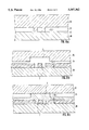
- FIGS. 8a to c show cross-sectional drawings for schematically illustrating the structure of the injection molding tools for producing the card structure shown in FIG. 3.
- FIG. 1 shows a schematic representation of a conventional chip card 1 with an embedded chip module 2 and a printed pattern 3.
- Such cards are currently produced either by the classical laminating technique, i.e. by welding together several plastic layers and embedding the chip module during the laminating operation, or by producing a multi- or one-layer card body and milling in a depression in which the chip module can be inserted.
- the third and currently cheapest technique is to produce the card body by injection molding, either providing the depression for the chip module in the card body during the injection process or already embedding the chip module itself in the plastic compound during the injection process. Outside the area where the chip module is provided, currently known injection molded cards have no additional features produced by injection molding that permit visual or automatic authenticity testing.
- FIG. 2 shows an inventive card body 1 in a simplified representation.
- This card body can have all the previous elements of customary injection molded cards, i.e. a chip module 2 or a printed pattern 3. But it furthermore contains at least one injection molding feature 4 that gives the card body a special character. This feature 4 is visually testable in a simple way and producible economically in large piece numbers but very difficult to imitate in single pieces (forgeries).
- Injection molding feature 4 in the present case a letter "H" disposed in a circular area, is a representative example of a company logo, letter or pictorial symbol of any structure.
- card body 1 is provided on the front with a white card surface against which circular area 8 stands out.
- FIG. 3 shows section A-B from FIG. 2.
- Card 1 is accordingly constructed of three layers, whereby layer 10 forming the front is white, back layer 12 is black and the middle layer is transparent.
- Front layer 10 and back layer 12 each have recesses that are likewise filled with the transparent plastic material of the middle layer.
- the recess on the front is of circular shape. It thus creates the contour of injection molding feature 4.
- the recesses in back cover layer 12 are in the form of pictorial symbol 7 so that symbol 7 is recognizable as a transparent "H" in black surroundings.
- Such a feature 4 can be tested in three steps, namely in transmitted light from the front. In this test one sees a transparent symbol 7 extending throughout the card thickness and embedded in the deeper black background of the card. On the back, symbol 7 is disposed in the all-over black background. Regarding the side edges of the card one likewise readily sees the three-layer structure due to the strongly contrasting layers. Bending tests show whether the card structure and in particular the two card surfaces are of seamless and homogeneous design.
- a hologram relief can be additionally provided in the surface of the back of the card during card production. This relief can be applied separately by the transfer method or be embossed during the injection process by providing such a relief in the injection mold.
- Such a hologram relief placed on side 6 of the card is readily recognizable over the total surface, i.e. both in the black card area and in the area of symbol 7, when suitably illuminated from the back. Inhomogeneities resulting from the piecing together of various parts of the card (forgery) are particularly easy to detect in this embodiment. From the front of the card only pictorial symbol 7 has holographic effects when sufficiently illuminated in transmitted light.
- inner layer 11 is provided with fluorescent substances the fluorescent effect can likewise be included in the testing of the card.
- feature 4 is a homogeneously embedded element.
- FIGS. 4a and 4b show a further variant of the inventive card structure.
- an opaque inner layer 17 is embedded between two transparent cover films 15 and 16.
- the opaque layer has a surface relief 23 on both sides that is recognizable as a relief from each side in incident light.
- the relief also appears darker in the thin areas than in the thick relief structures.
- transmitted light a reversal of the optical effect can likewise be detected as with an authentic watermark, i.e. in this case the thick relief areas appear dark and the thinner structures light.
- the embodiment shown in FIG. 4b is very similar, i.e. here too a reversal of the light/dark structures can be detected depending on whether they are regarded in transmitted light or in incident light.
- the effect is more powerful through transparent layer 18 than from back layer 19.
- the card area intended for the hologram (that may also extend over the entire card surface) is underlaid with a plastic compound with metallic luster or a very dark, preferably black, colored plastic material.
- the thickness of layer 21 is of lesser importance. It is only important for the invention that this layer is incorporated by injection molding and that the space of the injection mold adjacent this surface has a holographic relief which is embossed into black or metallescent surface 22.
- FIG. 6 shows an embodiment that uses incompatible plastic components for improving production operations.
- FIG. 6 shows a section through the chip card area in which a chip module is later to be inserted.
- This area comprises card body 1 provided with a stepped depression 42.
- Bottom area 41 has a wall thickness of about 100 micrometers. After the card blank is completed this area is printed from both sides in separate method steps. A chip module similar to element 43 is then inserted.
- the inventive principle provides for injecting incompatible plastic materials into stepped depression 42 in one of the injection molding units. This fills the depression with insert element 43 so that area 41 can be readily printed in subsequent printing operations.
- the various printing operations are over the card blank is for example bent over a curved surface to remove element 43. In this way it is easy to remove the insert element and replace it by a chip module.
- the embodiment example described with reference to FIG. 6 is particularly useful for producing injection molded cards that are printed and then equipped with the chip modules in separate operations. This application is recommendable both for single cards and in cases in which multicopy sheets are to be produced by the injection molding technique.
- FIG. 7 shows the schematic structure of a rotary table injection molding machine for producing e.g. a card in three separate injection operations (units A, B and C).
- the fourth unit E is provided for removing the card from the apparatus.
- the injection mold basically comprises two rotary tables, the upper one being rigid and the lower one being rotatable in the direction of arrow 26.
- the upper rotary table is also vertically displaceable by means of apparatus elements not shown so as to permit a raising and lowering of this mold part.
- the lower rotary table In the area of the four segments A to E the lower rotary table has depressions corresponding to the particular card shape. Depending on the embodiment the depth of these mold areas can be varied. In the present case it corresponds to the later card thickness.
- mold parts 35, 36 and 37 are provided in the mold parts of the upper rotary table. These structures are adapted to the particular layer areas 12, 11 and 10 to be produced.
- the different plastic components are injected into the mold via material feed means 30. After each injection operation the upper rotary table is raised and the lower rotary table turned further by one phase.
- layer 12 is injected in mold space 32 in the first unit (unit A). If a hologram relief is also to be produced on the back card surface, surface 40 must be equipped with such a relief. This can be done either by equipping the mold surface with the hologram relief or by inserting relief films that are replaced for each card or after a certain number of injection operations.
Abstract
The invention relates to a flat molding produced by the injection molding technique, in particular an identity card, chip card or the like, characterized in that it has different volume areas containing different plastic components and formed and disposed so as to be distinguishable from one another visually and/or by measuring technology.
Description
This application is a continuation of application Ser. No. 07/992,725, filed Dec. 18, 1992, now abandoned.
The present invention relates to a card produced by injection molding, in particular an identity card, chip card or the like, and to a method and apparatus for producing it.
In recent decades cards have become established in daily life in a great variety of areas. They are in use as identity cards, driver's licenses, access control cards, chip cards, credit cards, check guarantee cards and so on.
In the development of cards a trend has come about in the course of time according to which highest priority is given to their simple and inexpensive production. Cards have therefore passed from the original, extremely high-quality paper inlay card to the so-called all-plastic laminated card, and then to the injection molded card. Such cards are known for example from the publications, DE-C 23 08 876, EP-C 0 101 968, EP-C 0 197 847.
With paper inlay cards the antifalsification techniques known from paper-of-value manufacture were used to produce paper inlays that, embedded between transparent films, convey the esthetic impression of a paper of value while permitting visual and possibly also manual testing of the authenticity features customary in papers of value.
All-plastic laminated cards are, as their name says, constructed completely of plastic layers. The inlay in these cards can be equipped within certain limits with printed patterns equivalent to those in paper inlay cards, but it is either impossible or unreasonable for financial reasons to provide classical authenticity features suitable for human testing.
With injection molded cards, which can be produced extremely inexpensively like customary injection molded parts in injection molding machines, the quality of the printed pattern is again considerably reduced from today's point of view. Real advantages thus result only in the production of chip cards since the injection molding technique permits the card depressions required for embedding the chip modules to be produced in one operation during production of the card body, or even the chip module to be embedded in the card structure during the injection process.
In the further development of production techniques the possibility of human authenticity testing was thus increasingly abandoned in favor of cheaper production methods. With current injection molded cards, if they are chip cards, the electronic security can be increased to almost any degree by using ever more complicated integrated circuits, but the card structure as such is extremely simple and thus fairly unsuitable for strictly visual authenticity testing.
The problem of the invention is therefore to propose a card and a method and apparatus for producing it that take sufficient account not only of the aspect of inexpensive production in high piece numbers but also of the security aspect with respect to visual authenticity testing.
This problem is solved when the card structure has different volume areas containing different plastic components which are formed and disposed in such a way as to be distinguishable from one another visually and possibly also by machine.
The invention exploits the fact that at the current level of injection molding technology a great variety of both plastic components and foreign bodies can be processed in almost any desired arrangement and combination in multi-stage methods. If one utilizes these possibilities to produce a multicomponent card structure one can produce human features similar to those known from classical paper-of-value protection technology without neglecting the originally desired economizing effect.
It proves to be particularly advantageous that the invention goes on from classical card protection technology while utilizing up-to-date production techniques. Although the inventive card can have a great variety of visually testable card structures it can be readily integrated into common injection molding production methods. Along with the card properties provided for visual authenticity testing, further measures can be provided for facilitating the further processing of the cards or obtaining further production-related economizing effects.
Developments of the invention and further advantages thereof can be found in the embodiment examples described with reference to the drawing, in which:
FIG. 1 shows a conventional chip card from the front,
FIG. 2 shows an inventive multicomponent injection molded card with a visually testable authenticity structure,
FIGS. 3 to 5 show cross-sectional drawings of different variants of the inventive card structure,
FIG. 6 shows a cross-sectional drawing of a structural element for economizing card production further,
FIG. 7 shows a schematic diagram of an apparatus for producing inventive cards,
FIGS. 8a to c show cross-sectional drawings for schematically illustrating the structure of the injection molding tools for producing the card structure shown in FIG. 3.
FIG. 1 shows a schematic representation of a conventional chip card 1 with an embedded chip module 2 and a printed pattern 3. Such cards are currently produced either by the classical laminating technique, i.e. by welding together several plastic layers and embedding the chip module during the laminating operation, or by producing a multi- or one-layer card body and milling in a depression in which the chip module can be inserted. The third and currently cheapest technique is to produce the card body by injection molding, either providing the depression for the chip module in the card body during the injection process or already embedding the chip module itself in the plastic compound during the injection process. Outside the area where the chip module is provided, currently known injection molded cards have no additional features produced by injection molding that permit visual or automatic authenticity testing.
FIG. 2 shows an inventive card body 1 in a simplified representation. This card body can have all the previous elements of customary injection molded cards, i.e. a chip module 2 or a printed pattern 3. But it furthermore contains at least one injection molding feature 4 that gives the card body a special character. This feature 4 is visually testable in a simple way and producible economically in large piece numbers but very difficult to imitate in single pieces (forgeries).
FIG. 3 shows section A-B from FIG. 2. Card 1 is accordingly constructed of three layers, whereby layer 10 forming the front is white, back layer 12 is black and the middle layer is transparent. Front layer 10 and back layer 12 each have recesses that are likewise filled with the transparent plastic material of the middle layer. The recess on the front is of circular shape. It thus creates the contour of injection molding feature 4. The recesses in back cover layer 12 are in the form of pictorial symbol 7 so that symbol 7 is recognizable as a transparent "H" in black surroundings.
Such a feature 4 can be tested in three steps, namely in transmitted light from the front. In this test one sees a transparent symbol 7 extending throughout the card thickness and embedded in the deeper black background of the card. On the back, symbol 7 is disposed in the all-over black background. Regarding the side edges of the card one likewise readily sees the three-layer structure due to the strongly contrasting layers. Bending tests show whether the card structure and in particular the two card surfaces are of seamless and homogeneous design.
If the security of this card structure is to be further increased a hologram relief can be additionally provided in the surface of the back of the card during card production. This relief can be applied separately by the transfer method or be embossed during the injection process by providing such a relief in the injection mold.
Such a hologram relief placed on side 6 of the card is readily recognizable over the total surface, i.e. both in the black card area and in the area of symbol 7, when suitably illuminated from the back. Inhomogeneities resulting from the piecing together of various parts of the card (forgery) are particularly easy to detect in this embodiment. From the front of the card only pictorial symbol 7 has holographic effects when sufficiently illuminated in transmitted light.
If inner layer 11 is provided with fluorescent substances the fluorescent effect can likewise be included in the testing of the card.
It is also very easy to clarify the question of whether feature 4 is a homogeneously embedded element. One illuminates the card from the side edges, possibly using a specially provided apparatus, and regards pictorial symbol 4. Due to the guidance of light within inner layer 11 the pictorial symbol will "glow" in a very characteristic way. If feature 4 was inserted subsequently or put together from different layer elements this prevents the expected light-guiding effects, so that a genuine element 4 also differs from imitations very clearly in this test.
FIGS. 4a and 4b show a further variant of the inventive card structure. In FIG. 4a an opaque inner layer 17 is embedded between two transparent cover films 15 and 16. The opaque layer has a surface relief 23 on both sides that is recognizable as a relief from each side in incident light. Like an authentic watermark, the relief also appears darker in the thin areas than in the thick relief structures. In transmitted light a reversal of the optical effect can likewise be detected as with an authentic watermark, i.e. in this case the thick relief areas appear dark and the thinner structures light.
In terms of the optical effect the embodiment shown in FIG. 4b is very similar, i.e. here too a reversal of the light/dark structures can be detected depending on whether they are regarded in transmitted light or in incident light. However the effect is more powerful through transparent layer 18 than from back layer 19.
In special embodiments it may suffice to provide only one hologram on the card surface. In this case, as apparent from FIG. 5, the card area intended for the hologram (that may also extend over the entire card surface) is underlaid with a plastic compound with metallic luster or a very dark, preferably black, colored plastic material. The thickness of layer 21 is of lesser importance. It is only important for the invention that this layer is incorporated by injection molding and that the space of the injection mold adjacent this surface has a holographic relief which is embossed into black or metallescent surface 22.
Since the described layer structures and layer thicknesses can be produced relatively exactly these effects are very easy to detect by measuring technology if they are suitably dimensioned and designed. One thus not only has the possibility of visual testing but can also add special substances to the individual layers of the card structure and evaluate properties that are largely or completely concealed from visual testing. In this connection reference is made to magnetic effects, electrically conductive effects or luminescent effects in the invisible spectral range.
Departing from the embodiments described in FIGS. 3 to 5, whereby the inventive principle for producing special optical or measuring effects was described using compatible plastic materials, FIG. 6 shows an embodiment that uses incompatible plastic components for improving production operations.
FIG. 6 shows a section through the chip card area in which a chip module is later to be inserted. This area comprises card body 1 provided with a stepped depression 42. Bottom area 41 has a wall thickness of about 100 micrometers. After the card blank is completed this area is printed from both sides in separate method steps. A chip module similar to element 43 is then inserted.
When printing cards there was always the problem up to now that area 41 gave way to the pressure of the print roll so that errors in the printed pattern were produced in this area. Furthermore there is the danger of area 41 being damaged by mechanical action so that the card body becomes useless.
The inventive principle provides for injecting incompatible plastic materials into stepped depression 42 in one of the injection molding units. This fills the depression with insert element 43 so that area 41 can be readily printed in subsequent printing operations. When the various printing operations are over the card blank is for example bent over a curved surface to remove element 43. In this way it is easy to remove the insert element and replace it by a chip module.
The embodiment example described with reference to FIG. 6 is particularly useful for producing injection molded cards that are printed and then equipped with the chip modules in separate operations. This application is recommendable both for single cards and in cases in which multicopy sheets are to be produced by the injection molding technique.
FIG. 7 shows the schematic structure of a rotary table injection molding machine for producing e.g. a card in three separate injection operations (units A, B and C). The fourth unit E is provided for removing the card from the apparatus.
Referring to FIGS. 8a to c, the mode of functioning of the injection mold can be described as follows.
The injection mold basically comprises two rotary tables, the upper one being rigid and the lower one being rotatable in the direction of arrow 26. The upper rotary table is also vertically displaceable by means of apparatus elements not shown so as to permit a raising and lowering of this mold part. In the area of the four segments A to E the lower rotary table has depressions corresponding to the particular card shape. Depending on the embodiment the depth of these mold areas can be varied. In the present case it corresponds to the later card thickness.
In the mold parts of the upper rotary table the structures of mold parts 35, 36 and 37 are provided. These structures are adapted to the particular layer areas 12, 11 and 10 to be produced.
The different plastic components are injected into the mold via material feed means 30. After each injection operation the upper rotary table is raised and the lower rotary table turned further by one phase.
As apparent from FIG. 8a, layer 12 is injected in mold space 32 in the first unit (unit A). If a hologram relief is also to be produced on the back card surface, surface 40 must be equipped with such a relief. This can be done either by equipping the mold surface with the hologram relief or by inserting relief films that are replaced for each card or after a certain number of injection operations.
After the plastic material which is black in the described example has been injected in unit A the mold is cooled until the plastic compound solidifies. Upper mold part 35 is then raised and lower mold area 38 transported together with layer 12 to unit B. In unit B the mold part required for producing layer 11 is made available. Mold space 33 to be filled in unit B is positioned above layer 12 and in the present case filled with transparent plastic material. During this process both layer 11 extending over the entire card surface and the recesses provided in the area of the injection molding feature are filled with transparent material. After upper mold part 36 is raised and the lower rotary table rotated further the now two- layer card structure 12, 11 passes to unit C. Here the card structure is placed under mold part 37 for as yet lacking layer 10 to be injected in mold space 34.
After the card material is cooled and solidifies again the upper mold part is raised once again and the rotary table rotated further to pos. E for removal of the card.
It is obvious to the expert that the injection operations in units A, B and C take place at the same time, i.e. after two initial phases a finished card can be removed from unit E with each phase.
It is likewise obvious that one can use not only the card features explained with reference to FIGS. 3, 4 and 5 but also each feature per se or combinations of these features in one card. In addition one can emboss the depression for chip module 2 as well during the production of these cards. This can be done for example with the aid of a movable die to be pressed into the plastic compound while it is still ductile,
Without departing from the inventive principle it is of course also possible to embed foreign bodies in the card structure as well. These may be for example safeguarding threads or prefabricated inlay areas introduced into the mold, or chip modules that are pressed into the plastic compound in the last working step or placed in a previously produced cavity.
Although the production of the inventive cards has been described with reference to a rotary table injection molding machine the expert will appreciate that this can also be done with other apparatus, for example apparatus in which the individual units A, B, C are disposed in a row and the lower mold parts are clocked past under the units using a kind of endless transport system.
For the cards described in FIGS. 3 to 5 compatible plastic components are used that have the corresponding optical and measuring properties and bond intimately with one another in the particular transitional area when "injected over one another." The expert will know which plastics have this property and will select them together with the particular optical and measuring properties. The same holds for incompatible plastic components that are required for producing removable insert elements 43 (FIG. 6).
Claims (6)
1. A method of injection molding a composite plastic identification card body comprising:
in succession, injecting a first plastic resin portion into an injection mold to delimit a first portion only of the card body, said first portion including a recess; permitting the first resin portion to solidify in the mold; then while the first resin portion is in the mold injecting into the mold at least a second plastic resin portion to delimit at least a portion of the remainder of the card body including filling said recess; then permitting the at least second resin portion to solidify in the mold; then removing the composite card body from the mold, wherein one of the plastic resin portions is incompatible with the other, and whereby one solidified resin portion may be separated from the other after the composite card body is removed from the mold to thereby leave a recess in the card body.
2. A method of injection molding a composite plastic identification card body comprising:
in succession, injecting a first plastic resin portion into an injection mold and solidifying said first resin portion to form at least a partial first layer of said card body; then while the first resin portion is in the mold injection into the mold a second plastic resin portion and solidifying said second resin portion to form at least a partial second layer of said card body; then injecting into the mold and solidifying a third plastic resin portion to form a third layer of said card body overlying said second layer; said second layer being molded so as to extend through said first and third layers to the respective outer surfaces of said first and third layers; and then removing the composite card body from the mold.
3. The method as claimed in claim 2, wherein said second layer is molded so that it extends through said first and third layers at the same location in the card body.
4. The method as claimed in claim 3, wherein said second resin portion is selected from plastic resins that are transparent when solidified and said first and third plastic resin portions are selected from plastic resins that are not transparent when solidified.
5. The method as claimed in claim 4, including selecting said first plastic resin portion so that it is opaque when solidified and colored black, and selecting said third plastic resin portion so that it is opaque when solidified and colored white.
6. A method of injection molding a composite plastic identification card body comprising:
in succession, injecting a first plastic resin portion into an injection mold to form a transparent first card layer; permitting the first resin portion to solidify in the mold; then while the first resin portion is in the mold injecting into the mold at least a second plastic resin portion to form an opaque second layer extending over said first layer; then permitting the at least second resin portion to solidify in the mold; and injecting and solidifying a third plastic resin portion using a resin that forms a third card layer that is transparent and overlies said second card layer; said second card layer being molded with varied thickness that is opaque to different degrees and thereby exhibits dark and light areas when observed in incident light, with the dark areas being reversed to light areas and the light areas being reversed to dark areas when observed in transmitted light; and then removing the composite card body from the mold.
Priority Applications (1)
| Application Number | Priority Date | Filing Date | Title |
|---|---|---|---|
| US08/288,041 US5567362A (en) | 1991-12-20 | 1994-08-10 | Identity card and a method and apparatus for producing it |
Applications Claiming Priority (4)
| Application Number | Priority Date | Filing Date | Title |
|---|---|---|---|
| DE4142408A DE4142408A1 (en) | 1991-12-20 | 1991-12-20 | ID CARD AND METHOD AND DEVICE FOR PRODUCING THE SAME |
| DE4142408.5 | 1991-12-20 | ||
| US99272592A | 1992-12-18 | 1992-12-18 | |
| US08/288,041 US5567362A (en) | 1991-12-20 | 1994-08-10 | Identity card and a method and apparatus for producing it |
Related Parent Applications (1)
| Application Number | Title | Priority Date | Filing Date |
|---|---|---|---|
| US99272592A Continuation | 1991-12-20 | 1992-12-18 |
Publications (1)
| Publication Number | Publication Date |
|---|---|
| US5567362A true US5567362A (en) | 1996-10-22 |
Family
ID=6447773
Family Applications (1)
| Application Number | Title | Priority Date | Filing Date |
|---|---|---|---|
| US08/288,041 Expired - Fee Related US5567362A (en) | 1991-12-20 | 1994-08-10 | Identity card and a method and apparatus for producing it |
Country Status (6)
| Country | Link |
|---|---|
| US (1) | US5567362A (en) |
| EP (1) | EP0548858B1 (en) |
| JP (1) | JP3802078B2 (en) |
| AT (1) | ATE193390T1 (en) |
| DE (2) | DE4142408A1 (en) |
| SG (1) | SG46282A1 (en) |
Cited By (27)
| Publication number | Priority date | Publication date | Assignee | Title |
|---|---|---|---|---|
| US5673503A (en) * | 1995-12-08 | 1997-10-07 | Trend Plastics Inc. | Gaming chip with edge insert and process for fabricating same |
| US5817207A (en) * | 1995-10-17 | 1998-10-06 | Leighton; Keith R. | Radio frequency identification card and hot lamination process for the manufacture of radio frequency identification cards |
| EP0964417A2 (en) * | 1998-06-08 | 1999-12-15 | Lucent Technologies Inc. | Article comprising co-injection molded component having integral light guide |
| EP0974928A2 (en) * | 1998-07-23 | 2000-01-26 | Orga Kartensysteme GmbH | Chip card |
| US6036099A (en) * | 1995-10-17 | 2000-03-14 | Leighton; Keith | Hot lamination process for the manufacture of a combination contact/contactless smart card and product resulting therefrom |
| US6297077B1 (en) * | 1997-08-20 | 2001-10-02 | Orga Kartensysteme Gmbh | Process for manufacturing chip cards, device for the implementation of this process and chip card |
| WO2001098087A1 (en) * | 1998-02-05 | 2001-12-27 | Safecard Id System, Inc. | Methods of creating a tamper resistant informational article |
| US6441736B1 (en) | 1999-07-01 | 2002-08-27 | Keith R. Leighton | Ultra-thin flexible durable radio frequency identification devices and hot or cold lamination process for the manufacture of ultra-thin flexible durable radio frequency identification devices |
| US6531080B1 (en) * | 1997-03-06 | 2003-03-11 | Institut Fur Mikrotechnik Mainz Gmbh | Method for producing and magazining micro-components |
| US6575371B1 (en) * | 1997-05-20 | 2003-06-10 | Giesecke & Devrient Gmbh | Injection-moulded card with decorative layer |
| US20030197905A1 (en) * | 2001-04-19 | 2003-10-23 | Gelardi John A. | Molded hologram apparatus method and product |
| US20040075189A1 (en) * | 2002-10-16 | 2004-04-22 | Ching-Lin Tai | Method for making dual-color melamine container |
| US20040075190A1 (en) * | 2002-10-16 | 2004-04-22 | Ching-Lin Tai | Method for making melamine container with dual-side patterns |
| US20040081851A1 (en) * | 2001-08-29 | 2004-04-29 | Niko Eiden | Method of Making Illuminated Covers |
| EP1533749A1 (en) * | 2002-07-01 | 2005-05-25 | Shinya Fukui | Material containing coding information, method of identification thereof and identification system therefor |
| WO2006054097A1 (en) * | 2004-11-17 | 2006-05-26 | Brite Ip Limited | Moulded leaved article |
| WO2006054072A1 (en) | 2004-11-17 | 2006-05-26 | Brite Ip Limited | Moulded insert page |
| CN100405798C (en) * | 2002-01-07 | 2008-07-23 | 诺基亚有限公司 | Illuminated covers |
| US20090127344A1 (en) * | 2003-12-10 | 2009-05-21 | Andreas Dostmann | Identification card and the production method thereof |
| US20090206164A1 (en) * | 2005-08-19 | 2009-08-20 | Stefan Kluge | Card-shaped data carrier |
| US20100001077A1 (en) * | 2005-08-19 | 2010-01-07 | Stefan Kluge | Card-shaped data carrier |
| US20100276495A1 (en) * | 2009-04-30 | 2010-11-04 | Arthur Blank & Company, Inc. | Transaction card assembly and methods of manufacture |
| US20130004725A1 (en) * | 2010-02-04 | 2013-01-03 | Nifco Inc. | Two-color molded article and process for production thereof |
| US20150085285A1 (en) * | 2013-09-23 | 2015-03-26 | Morphotrust Usa, Llc | Unidirectional Opacity Watermark |
| WO2017066464A1 (en) * | 2015-10-14 | 2017-04-20 | Capital One Services, Llc | Molded pocket in transaction card construction |
| US10479128B2 (en) * | 2017-10-27 | 2019-11-19 | Assa Abloy Ab | Security feature |
| US10675833B2 (en) * | 2015-04-13 | 2020-06-09 | Keter Plastic Ltd. | Multilayered injection molded interlace-like article and method for molding same |
Families Citing this family (9)
| Publication number | Priority date | Publication date | Assignee | Title |
|---|---|---|---|---|
| JP2000514581A (en) * | 1996-07-15 | 2000-10-31 | オーストリア カード プラスティッカルテン ウント アウスヴァイスジステーム ゲゼルシャフト ミット ベシュレンクテル ハフツング | Data carrier with module and hologram |
| DE19736063C2 (en) * | 1997-08-20 | 2000-01-05 | Orga Kartensysteme Gmbh | Smart card |
| DE10013410B4 (en) * | 2000-03-17 | 2011-05-05 | Ovd Kinegram Ag | Laminate, in particular in the form of cards, and process for its production |
| DE10110939B4 (en) * | 2001-03-07 | 2004-07-08 | Mühlbauer Ag | Method and device for hot press connecting a chip module to a carrier substrate |
| DE102004023310A1 (en) * | 2004-05-11 | 2005-12-15 | Giesecke & Devrient Gmbh | Multi-layered portable data carrier |
| DE102013201945A1 (en) * | 2013-02-06 | 2014-08-07 | Bundesdruckerei Gmbh | Security feature for a value or security product and method of making the security feature |
| JP5852974B2 (en) * | 2013-02-25 | 2016-02-03 | 株式会社川崎合成樹脂 | Manufacturing method of mortarboard |
| DE102015100208A1 (en) * | 2015-01-09 | 2016-07-14 | Leonhard Kurz Stiftung & Co. Kg | Process for producing a composite article and a composite article |
| CN105160993B (en) * | 2015-08-26 | 2017-11-21 | 杭州沃朴物联科技有限公司 | A kind of stereochemical structure figure antifalsification label and preparation method thereof |
Citations (8)
| Publication number | Priority date | Publication date | Assignee | Title |
|---|---|---|---|---|
| US2226408A (en) * | 1936-07-21 | 1940-12-24 | New Brunswick Die Molding Corp | Apparatus for manufacturing compound molded bodies |
| US2333059A (en) * | 1941-01-08 | 1943-10-26 | Hydraulic Dev Corp Inc | Two color injection die |
| US3031722A (en) * | 1957-11-27 | 1962-05-01 | Joseph A Gits | Methods of making molded articles |
| US3363039A (en) * | 1963-08-09 | 1968-01-09 | Asahi Dow Ltd | Injection molding processes for thermoplastic materials |
| JPS6280028A (en) * | 1985-10-03 | 1987-04-13 | Toppan Printing Co Ltd | Manufacture of molded piece having partly deposited hologram |
| JPS62233234A (en) * | 1986-04-03 | 1987-10-13 | Toppan Printing Co Ltd | Manufacture of molded object having hologram |
| US5030406A (en) * | 1989-08-14 | 1991-07-09 | Sorensen Jens Ole | Sequentially injected multi-component shuttle-stack-molding |
| US5045268A (en) * | 1989-12-11 | 1991-09-03 | Sorensen Jens Ole | Cross-lamination injection molding |
Family Cites Families (8)
| Publication number | Priority date | Publication date | Assignee | Title |
|---|---|---|---|---|
| GB1264369A (en) * | 1968-12-05 | 1972-02-23 | ||
| DE3048733C2 (en) * | 1980-12-23 | 1983-06-16 | GAO Gesellschaft für Automation und Organisation mbH, 8000 München | "Identity card and process for producing the same" |
| DE3231460A1 (en) * | 1982-08-24 | 1984-03-01 | GAO Gesellschaft für Automation und Organisation mbH, 8000 München | ID CARD WITH CHECKABLE CHARACTERISTICS |
| US4469725A (en) * | 1982-09-14 | 1984-09-04 | Fis Organisation Ag | Identification card |
| CH659433A5 (en) * | 1982-10-04 | 1987-01-30 | Landis & Gyr Ag | DOCUMENT WITH A REFLECTIVE OPTICAL SECURITY ELEMENT. |
| EP0429448B1 (en) * | 1988-02-05 | 1994-04-13 | Primtec | Stabilized injection molding when using a common mold part with separate complementary mold parts |
| KR900702481A (en) * | 1988-06-21 | 1990-12-07 | 원본미기재 | How to manufacture a portable electronic token |
| JP2559834B2 (en) * | 1989-01-12 | 1996-12-04 | 三菱電機株式会社 | IC card |
-
1991
- 1991-12-20 DE DE4142408A patent/DE4142408A1/en not_active Withdrawn
-
1992
- 1992-12-18 AT AT92121642T patent/ATE193390T1/en active
- 1992-12-18 DE DE59209840T patent/DE59209840D1/en not_active Expired - Fee Related
- 1992-12-18 SG SG1996002092A patent/SG46282A1/en unknown
- 1992-12-18 EP EP92121642A patent/EP0548858B1/en not_active Expired - Lifetime
- 1992-12-21 JP JP35539992A patent/JP3802078B2/en not_active Expired - Fee Related
-
1994
- 1994-08-10 US US08/288,041 patent/US5567362A/en not_active Expired - Fee Related
Patent Citations (8)
| Publication number | Priority date | Publication date | Assignee | Title |
|---|---|---|---|---|
| US2226408A (en) * | 1936-07-21 | 1940-12-24 | New Brunswick Die Molding Corp | Apparatus for manufacturing compound molded bodies |
| US2333059A (en) * | 1941-01-08 | 1943-10-26 | Hydraulic Dev Corp Inc | Two color injection die |
| US3031722A (en) * | 1957-11-27 | 1962-05-01 | Joseph A Gits | Methods of making molded articles |
| US3363039A (en) * | 1963-08-09 | 1968-01-09 | Asahi Dow Ltd | Injection molding processes for thermoplastic materials |
| JPS6280028A (en) * | 1985-10-03 | 1987-04-13 | Toppan Printing Co Ltd | Manufacture of molded piece having partly deposited hologram |
| JPS62233234A (en) * | 1986-04-03 | 1987-10-13 | Toppan Printing Co Ltd | Manufacture of molded object having hologram |
| US5030406A (en) * | 1989-08-14 | 1991-07-09 | Sorensen Jens Ole | Sequentially injected multi-component shuttle-stack-molding |
| US5045268A (en) * | 1989-12-11 | 1991-09-03 | Sorensen Jens Ole | Cross-lamination injection molding |
Cited By (48)
| Publication number | Priority date | Publication date | Assignee | Title |
|---|---|---|---|---|
| US6214155B1 (en) | 1995-10-17 | 2001-04-10 | Keith R. Leighton | Radio frequency identification card and hot lamination process for the manufacture of radio frequency identification cards |
| US5817207A (en) * | 1995-10-17 | 1998-10-06 | Leighton; Keith R. | Radio frequency identification card and hot lamination process for the manufacture of radio frequency identification cards |
| US6514367B1 (en) | 1995-10-17 | 2003-02-04 | Keith R. Leighton | Hot lamination process for the manufacture of a combination contact/contactless smart card |
| USRE40145E1 (en) | 1995-10-17 | 2008-03-11 | Leighton Technologies Llc | Ultra-thin flexible durable radio frequency identification devices and hot or cold lamination process for the manufacture of ultra-thin flexible durable radio frequency identification devices |
| US6036099A (en) * | 1995-10-17 | 2000-03-14 | Leighton; Keith | Hot lamination process for the manufacture of a combination contact/contactless smart card and product resulting therefrom |
| US5673503A (en) * | 1995-12-08 | 1997-10-07 | Trend Plastics Inc. | Gaming chip with edge insert and process for fabricating same |
| US6851174B2 (en) | 1997-03-06 | 2005-02-08 | Institut Fur Mikrotechnik Mainz Gmbh | Integrally cast magazine for microcomponents |
| US6531080B1 (en) * | 1997-03-06 | 2003-03-11 | Institut Fur Mikrotechnik Mainz Gmbh | Method for producing and magazining micro-components |
| US6575371B1 (en) * | 1997-05-20 | 2003-06-10 | Giesecke & Devrient Gmbh | Injection-moulded card with decorative layer |
| US6297077B1 (en) * | 1997-08-20 | 2001-10-02 | Orga Kartensysteme Gmbh | Process for manufacturing chip cards, device for the implementation of this process and chip card |
| WO2001098087A1 (en) * | 1998-02-05 | 2001-12-27 | Safecard Id System, Inc. | Methods of creating a tamper resistant informational article |
| EP0964417A3 (en) * | 1998-06-08 | 2000-11-29 | Lucent Technologies Inc. | Article comprising co-injection molded component having integral light guide |
| EP0964417A2 (en) * | 1998-06-08 | 1999-12-15 | Lucent Technologies Inc. | Article comprising co-injection molded component having integral light guide |
| EP0974928A2 (en) * | 1998-07-23 | 2000-01-26 | Orga Kartensysteme GmbH | Chip card |
| EP0974928A3 (en) * | 1998-07-23 | 2001-01-24 | Orga Kartensysteme GmbH | Chip card |
| US6441736B1 (en) | 1999-07-01 | 2002-08-27 | Keith R. Leighton | Ultra-thin flexible durable radio frequency identification devices and hot or cold lamination process for the manufacture of ultra-thin flexible durable radio frequency identification devices |
| US20030197905A1 (en) * | 2001-04-19 | 2003-10-23 | Gelardi John A. | Molded hologram apparatus method and product |
| US6929761B2 (en) | 2001-04-19 | 2005-08-16 | Sagoma Plastics Corporation | Molded hologram apparatus method and product |
| US20040081851A1 (en) * | 2001-08-29 | 2004-04-29 | Niko Eiden | Method of Making Illuminated Covers |
| US6773644B1 (en) * | 2001-08-29 | 2004-08-10 | Nokia Corporation | Method of making illuminated covers |
| US6790396B2 (en) * | 2001-08-29 | 2004-09-14 | Nokia Corporation | Method of making illuminated covers |
| CN100405798C (en) * | 2002-01-07 | 2008-07-23 | 诺基亚有限公司 | Illuminated covers |
| US20060091220A1 (en) * | 2002-07-01 | 2006-05-04 | Shinya Fukui | Material containing coding information method of identification thereof and identification system therefor |
| EP1533749A4 (en) * | 2002-07-01 | 2005-09-21 | Shinya Fukui | Material containing coding information, method of identification thereof and identification system therefor |
| EP1533749A1 (en) * | 2002-07-01 | 2005-05-25 | Shinya Fukui | Material containing coding information, method of identification thereof and identification system therefor |
| US20040075190A1 (en) * | 2002-10-16 | 2004-04-22 | Ching-Lin Tai | Method for making melamine container with dual-side patterns |
| US20040075189A1 (en) * | 2002-10-16 | 2004-04-22 | Ching-Lin Tai | Method for making dual-color melamine container |
| US20090127344A1 (en) * | 2003-12-10 | 2009-05-21 | Andreas Dostmann | Identification card and the production method thereof |
| WO2006054097A1 (en) * | 2004-11-17 | 2006-05-26 | Brite Ip Limited | Moulded leaved article |
| WO2006054072A1 (en) | 2004-11-17 | 2006-05-26 | Brite Ip Limited | Moulded insert page |
| US20090206164A1 (en) * | 2005-08-19 | 2009-08-20 | Stefan Kluge | Card-shaped data carrier |
| US20100001077A1 (en) * | 2005-08-19 | 2010-01-07 | Stefan Kluge | Card-shaped data carrier |
| US9579921B2 (en) | 2005-08-19 | 2017-02-28 | Giesecke & Devrient Gmbh | Card-shaped data carrier |
| US8226014B2 (en) | 2005-08-19 | 2012-07-24 | Giesecke & Devrient Gmbh | Card-shaped data carrier |
| US8690064B2 (en) | 2009-04-30 | 2014-04-08 | Abnote Usa, Inc. | Transaction card assembly and methods of manufacture |
| US20100276495A1 (en) * | 2009-04-30 | 2010-11-04 | Arthur Blank & Company, Inc. | Transaction card assembly and methods of manufacture |
| US20130004725A1 (en) * | 2010-02-04 | 2013-01-03 | Nifco Inc. | Two-color molded article and process for production thereof |
| US9259869B2 (en) * | 2010-02-04 | 2016-02-16 | Nifco Inc. | Two-color molded article and process for production thereof |
| US20150085285A1 (en) * | 2013-09-23 | 2015-03-26 | Morphotrust Usa, Llc | Unidirectional Opacity Watermark |
| US9855720B2 (en) * | 2013-09-23 | 2018-01-02 | Morphotrust Usa, Llc | Unidirectional opacity watermark |
| US10675833B2 (en) * | 2015-04-13 | 2020-06-09 | Keter Plastic Ltd. | Multilayered injection molded interlace-like article and method for molding same |
| US10207436B2 (en) | 2015-10-14 | 2019-02-19 | Capital One Services, Llc | Molded pocket in transaction card construction |
| EP3362248A4 (en) * | 2015-10-14 | 2019-05-08 | Capital One Services, LLC | Molded pocket in transaction card construction |
| US10335985B2 (en) | 2015-10-14 | 2019-07-02 | Capital One Services, Llc | Molded pocket in transaction card construction |
| WO2017066464A1 (en) * | 2015-10-14 | 2017-04-20 | Capital One Services, Llc | Molded pocket in transaction card construction |
| US10946565B2 (en) | 2015-10-14 | 2021-03-16 | Capital One Services, Llc | Molded pocket in transaction card construction |
| US11034065B2 (en) | 2015-10-14 | 2021-06-15 | Capital One Services, Llc | Molded pocket in transaction card construction |
| US10479128B2 (en) * | 2017-10-27 | 2019-11-19 | Assa Abloy Ab | Security feature |
Also Published As
| Publication number | Publication date |
|---|---|
| EP0548858B1 (en) | 2000-05-24 |
| ATE193390T1 (en) | 2000-06-15 |
| EP0548858A1 (en) | 1993-06-30 |
| JP3802078B2 (en) | 2006-07-26 |
| SG46282A1 (en) | 1998-02-20 |
| DE4142408A1 (en) | 1993-06-24 |
| JPH05278067A (en) | 1993-10-26 |
| DE59209840D1 (en) | 2000-06-29 |
Similar Documents
| Publication | Publication Date | Title |
|---|---|---|
| US5567362A (en) | Identity card and a method and apparatus for producing it | |
| JP2731918B2 (en) | Identification card and method of manufacturing the same | |
| CN102083632B (en) | Security element and method for the production thereof | |
| RU2264920C2 (en) | Data carrier, method for manufacturing data carrier and printing form for metallographic printing | |
| KR101119655B1 (en) | Security substrate incorporating elongate security elements and security article | |
| DE102007024298B3 (en) | Film element for authentication, security paper, security document, security document, coin, token, commodity, design element and method for producing a film element for authentication and method for producing a security paper, a security document and a value document such as a banknote | |
| US6827283B2 (en) | Product with a security element | |
| US6337752B1 (en) | Data carrier having an optically variable element and methods for producing it | |
| US7894112B2 (en) | Security element with a diffraction structure having subareas representing recognizable information | |
| US4735670A (en) | Method of producing an identification card | |
| US4564409A (en) | Planar card made of a thermoplastic material having visually recognizable safety markings and method of manufacturing such card | |
| US20060197337A1 (en) | Identification document with lenticular watermark | |
| UA81266C2 (en) | Security paper | |
| UA84401C2 (en) | security element, method of its manufacturing (variants), security paper and security document | |
| JPH0530640B2 (en) | ||
| JPH021394A (en) | Certificate with surface relief and manufacture thereof | |
| US5958528A (en) | Data carrier and method for producting it | |
| CN101678696A (en) | Security and/or valuable document having at least two different security features which are positioned precisely to register | |
| US20090127344A1 (en) | Identification card and the production method thereof | |
| JPH04273392A (en) | Data medium and manufacture thereof | |
| EP3634774B1 (en) | Forge-proof document | |
| EP1388808A1 (en) | Data carrier | |
| WO2010043674A1 (en) | Identification document with colored personalization inside | |
| WO1984002309A1 (en) | Plastics card for security, identity or banking purposes | |
| US20030205623A1 (en) | Method of manufacturing a card with anti-counterfeit differentiable mark |
Legal Events
| Date | Code | Title | Description |
|---|---|---|---|
| FEPP | Fee payment procedure |
Free format text: PAYOR NUMBER ASSIGNED (ORIGINAL EVENT CODE: ASPN); ENTITY STATUS OF PATENT OWNER: LARGE ENTITY |
|
| FPAY | Fee payment |
Year of fee payment: 4 |
|
| REMI | Maintenance fee reminder mailed | ||
| LAPS | Lapse for failure to pay maintenance fees | ||
| STCH | Information on status: patent discontinuation |
Free format text: PATENT EXPIRED DUE TO NONPAYMENT OF MAINTENANCE FEES UNDER 37 CFR 1.362 |
|
| FP | Lapsed due to failure to pay maintenance fee |
Effective date: 20041022 |