US5557596A - Ultra-high density storage device - Google Patents
Ultra-high density storage device Download PDFInfo
- Publication number
- US5557596A US5557596A US08/501,432 US50143295A US5557596A US 5557596 A US5557596 A US 5557596A US 50143295 A US50143295 A US 50143295A US 5557596 A US5557596 A US 5557596A
- Authority
- US
- United States
- Prior art keywords
- storage
- recited
- storage device
- storage area
- electron beam
- Prior art date
- Legal status (The legal status is an assumption and is not a legal conclusion. Google has not performed a legal analysis and makes no representation as to the accuracy of the status listed.)
- Expired - Lifetime
Links
Images


Classifications
-
- G—PHYSICS
- G11—INFORMATION STORAGE
- G11B—INFORMATION STORAGE BASED ON RELATIVE MOVEMENT BETWEEN RECORD CARRIER AND TRANSDUCER
- G11B9/00—Recording or reproducing using a method not covered by one of the main groups G11B3/00 - G11B7/00; Record carriers therefor
- G11B9/10—Recording or reproducing using a method not covered by one of the main groups G11B3/00 - G11B7/00; Record carriers therefor using electron beam; Record carriers therefor
-
- Y—GENERAL TAGGING OF NEW TECHNOLOGICAL DEVELOPMENTS; GENERAL TAGGING OF CROSS-SECTIONAL TECHNOLOGIES SPANNING OVER SEVERAL SECTIONS OF THE IPC; TECHNICAL SUBJECTS COVERED BY FORMER USPC CROSS-REFERENCE ART COLLECTIONS [XRACs] AND DIGESTS
- Y10—TECHNICAL SUBJECTS COVERED BY FORMER USPC
- Y10S—TECHNICAL SUBJECTS COVERED BY FORMER USPC CROSS-REFERENCE ART COLLECTIONS [XRACs] AND DIGESTS
- Y10S977/00—Nanotechnology
- Y10S977/84—Manufacture, treatment, or detection of nanostructure
- Y10S977/849—Manufacture, treatment, or detection of nanostructure with scanning probe
- Y10S977/86—Scanning probe structure
- Y10S977/861—Scanning tunneling probe
-
- Y—GENERAL TAGGING OF NEW TECHNOLOGICAL DEVELOPMENTS; GENERAL TAGGING OF CROSS-SECTIONAL TECHNOLOGIES SPANNING OVER SEVERAL SECTIONS OF THE IPC; TECHNICAL SUBJECTS COVERED BY FORMER USPC CROSS-REFERENCE ART COLLECTIONS [XRACs] AND DIGESTS
- Y10—TECHNICAL SUBJECTS COVERED BY FORMER USPC
- Y10S—TECHNICAL SUBJECTS COVERED BY FORMER USPC CROSS-REFERENCE ART COLLECTIONS [XRACs] AND DIGESTS
- Y10S977/00—Nanotechnology
- Y10S977/84—Manufacture, treatment, or detection of nanostructure
- Y10S977/849—Manufacture, treatment, or detection of nanostructure with scanning probe
- Y10S977/86—Scanning probe structure
- Y10S977/863—Atomic force probe
-
- Y—GENERAL TAGGING OF NEW TECHNOLOGICAL DEVELOPMENTS; GENERAL TAGGING OF CROSS-SECTIONAL TECHNOLOGIES SPANNING OVER SEVERAL SECTIONS OF THE IPC; TECHNICAL SUBJECTS COVERED BY FORMER USPC CROSS-REFERENCE ART COLLECTIONS [XRACs] AND DIGESTS
- Y10—TECHNICAL SUBJECTS COVERED BY FORMER USPC
- Y10S—TECHNICAL SUBJECTS COVERED BY FORMER USPC CROSS-REFERENCE ART COLLECTIONS [XRACs] AND DIGESTS
- Y10S977/00—Nanotechnology
- Y10S977/84—Manufacture, treatment, or detection of nanostructure
- Y10S977/849—Manufacture, treatment, or detection of nanostructure with scanning probe
- Y10S977/86—Scanning probe structure
- Y10S977/868—Scanning probe structure with optical means
- Y10S977/869—Optical microscope
-
- Y—GENERAL TAGGING OF NEW TECHNOLOGICAL DEVELOPMENTS; GENERAL TAGGING OF CROSS-SECTIONAL TECHNOLOGIES SPANNING OVER SEVERAL SECTIONS OF THE IPC; TECHNICAL SUBJECTS COVERED BY FORMER USPC CROSS-REFERENCE ART COLLECTIONS [XRACs] AND DIGESTS
- Y10—TECHNICAL SUBJECTS COVERED BY FORMER USPC
- Y10S—TECHNICAL SUBJECTS COVERED BY FORMER USPC CROSS-REFERENCE ART COLLECTIONS [XRACs] AND DIGESTS
- Y10S977/00—Nanotechnology
- Y10S977/84—Manufacture, treatment, or detection of nanostructure
- Y10S977/88—Manufacture, treatment, or detection of nanostructure with arrangement, process, or apparatus for testing
- Y10S977/881—Microscopy or spectroscopy, e.g. sem, tem
-
- Y—GENERAL TAGGING OF NEW TECHNOLOGICAL DEVELOPMENTS; GENERAL TAGGING OF CROSS-SECTIONAL TECHNOLOGIES SPANNING OVER SEVERAL SECTIONS OF THE IPC; TECHNICAL SUBJECTS COVERED BY FORMER USPC CROSS-REFERENCE ART COLLECTIONS [XRACs] AND DIGESTS
- Y10—TECHNICAL SUBJECTS COVERED BY FORMER USPC
- Y10S—TECHNICAL SUBJECTS COVERED BY FORMER USPC CROSS-REFERENCE ART COLLECTIONS [XRACs] AND DIGESTS
- Y10S977/00—Nanotechnology
- Y10S977/902—Specified use of nanostructure
- Y10S977/932—Specified use of nanostructure for electronic or optoelectronic application
- Y10S977/943—Information storage or retrieval using nanostructure
Definitions
- the present invention relates generally to storage devices, and more particularly to storage devices based on field emitters.
- SPM Scanned Probe Microscopy
- a probe is positioned extremely close to a storage medium.
- STM Scanning Tunnelling Microscopy
- the probe is within a few nanometers of the medium to ensure that the probe is within the tunnelling range of the medium.
- the storage device preferably should have fast access times and high data rates.
- the present invention is a ultra-high density storage device.
- the present invention has fast access times and high data rates.
- the invented storage device is based on a technology different from any of the conventional storage devices. It is based on field emitters, which are made by standard semiconductor microfabrication technology, and which emit beams of electrons from very sharp points.
- the storage device includes many field emitters, a storage medium and a micromover.
- the storage medium has many storage areas, and the field emitters are spaced apart to have one emitter responsible for a number of storage areas on the storage medium. In one preferred embodiment, each storage area is responsible for one bit of the storage device.
- the medium is in close proximity to the field emitters, such as a few hundredths of a micrometer to a few micrometers away.
- Each field emitter generates an electron beam current.
- Each storage area can be in one of a few different states.
- binary information is stored in the areas, with one state representing a high bit and another state representing a low bit.
- Information can be written onto the storage areas using the electron beams.
- the magnitude of each electron beam can be increased to a preselected level to change the state of the storage area on which it impinges. By changing the state of a storage area, one writes information onto it.
- the micromover is made by semiconductor microfabrication techniques.
- the micromover scans the storage medium with respect to the field emitters or vice versa.
- each emitter can access information from a number of storage areas on the medium.
- the storage device has very fast access times and data rates.
- FIGS. 1A-1B show different perspectives of a preferred embodiment of the invention.
- FIG. 1C shows the top view of the cross section A--A in FIG. 1A.
- FIG. 2 shows the field emitters reading from storage areas in one embodiment of the present invention.
- FIG. 3 shows the storage medium in the present invention based on a diode structure.
- FIGS. 4A-4B show different preferred diode structures as storage media in the present invention.
- FIG. 5 shows the storage medium in the present invention based on a florescent material.
- FIGS. 1-5 Same numerals in FIGS. 1-5 are assigned to similar elements in all the figures. Embodiments of the invention are discussed below with reference to FIGS. 1-5. However, those skilled in the art will readily appreciate that the detailed description given herein with respect to these figures is for explanatory purposes as the invention extends beyond these limited embodiments.
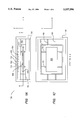
- FIG. 1A shows a side cross section view of a preferred embodiment 100 of the invention. It includes a number of field emitters, such as 102 and 104, a storage medium 106 with a number of storage areas, such as 108, and a micromover 110, which scans the storage medium 106 with respect to the field emitters or vice versa.
- each storage area is responsible for storing one bit of information.
- the field emitters are point-emitters with very sharp points; each may have a radius of curvature of about one nanometer to hundreds of nanometers.
- a preselected potential difference is applied between a field emitter and its corresponding gate, such as between the emitter 102 and its circular gate 103 surrounding it. Due to the sharp point of the emitter, an electron beam current is extracted from the emitter towards the storage area.
- a voltage may also be applied to the storage medium 106 to either accelerate or decelerate the field-emitted electrons or to aid in focusing the field-emitted electrons.
- the casing 120 keeps the storage medium 106 in partial vacuum, such as at least 10 -5 torr.
- partial vacuum such as at least 10 -5 torr.
- Different researchers have fabricated such types of microfabricated field emitters in vacuum cavities using semiconductor processing techniques. See, for example, "Silicon Field Emission Transistors and Diodes,” by Jones, published in IEEE Transactions on Components, Hybrids and Manufacturing Technology, 15, page 1051, 1992.
- each field emitter has a corresponding storage area.
- each field emitter is responsible for a number of storage areas. As the micromover 110 scans the medium 106 to different locations, each emitter is positioned above different storage areas. With the micromover 110, an array of field emitters can scan over the storage medium.
- the field emitters are responsible to read and write information on the storage areas by means of the electron beams they produce.
- the field emitters suitable for the present invention are the type that can produce electron beams that are narrow enough to achieve the desired bit density of the storage medium, and can provide the power density of the beam current needed for reading from and writing to the medium.
- a variety of ways are known in the art that are suitable to make such field emitters. For example, one method is disclosed in "Physical Properties of Thin-Film Field Emission Cathodes With Molybdenum Cones," by Spindt et al, published in the Journal of Applied Physics, Vol. 47, No. 12, December 1976.
- there can be a two-dimensional array of emitters such as 100 by 100 emitters, with an emitter pitch of 50 micrometers in both the X and the Y directions.
- Each emitter may access bits in tens of thousands to hundreds of millions of storage areas.
- the emitters scan over the storage medium that has a two dimensional array of storage areas, with a periodicity of about 1 to 100 nanometers between any two storage areas and the range of the micromover is 50 micrometers.
- all the emitters may be addressed simultaneously or in a multiplexed manner.
- Such a parallel accessing scheme significantly reduces access time, and increases data rate of the storage device.
- FIG. 1B shows the top view of the storage medium in a preferred embodiment illustrating a two dimensional array of storage areas and a two dimensional array of emitters.
- Addressing the storage areas requires external circuits.
- One preferred embodiment to reduce the number of external circuits is to separate the storage medium into rows, such as the row 140, where each row contains a number of storage areas.
- Each emitter is responsible for a number of rows. However, in this preferred embodiment, each emitter is not responsible for the entire length of the rows.
- the emitter 102 is responsible for the storage areas within the rows 140 through 142, and within the columns 144 through 146. All rows of storage areas accessed by one emitter are connected to one external circuit, for example rows 140 through 142.
- To address a storage area one activates the emitter responsible for that storage area and moves that emitter by the micromover to that storage area.
- the preferred micromover 110 can also be made in a variety of ways, as long as it has sufficient range and resolution to position the field emitters over the storage areas.
- the micromover 110 is fabricated by standard semiconductor microfabrication process to scan the medium 106 in the X and Y directions with respect to the casing 120.
- FIG. 1C shows the top view of the cross section A--A in FIG. 1A, illustrating the storage medium being held by two sets of thin-walled microfabricated beams.
- the faces of the first set of thin-walled beams are in the Y-Z plane, such as 112 and 114; this set of beams may be flexed in the X direction allowing the medium to move in the X direction with respect to the casing 120.
- the faces of the second set of thin-walled beams are in the X-Z plane, such as 116 and 118; this set of beams allow the medium to move in the Y direction with respect to the casing 120.
- the medium is held by the first set of beams, which are connected to a frame 122.
- the frame 122 is held by the second set of beams, which are connected to the casing 120.
- the field emitters scan over the medium, or the medium scans over the field emitters in the X-Y directions by electrostatic, electromagnetic or piezoelectric means known in the art.
- the micromover 110 includes the structure holding and moving the storage medium relative to the field emitters.
- the electron beam currents are rastered over the surface of the storage medium 106 by either electrostatically or electromagnetically deflecting them, such as by electrostatic deflectors like the electrode 125 positioned adjacent to the emitter 104.
- electrostatic deflectors like the electrode 125 positioned adjacent to the emitter 104.
- writing is accomplished by temporarily increasing the power density of the electron beam current to modify the surface state of the storage area; and reading is accomplished by observing the effect of the storage area on the electron beams, or the effect of the electron beams on the storage area.
- a storage area that has been modified can represent a bit 1
- a storage area that has not been modified can represent a bit 0.
- the permanently modified storage medium is suitable for write-once-read-many memory (WORM).
- the basic idea is to alter the structure of the storage area in such a way as to vary its secondary electron emission coefficient (SEEC), its backscattered electron coefficient (BEC), or the collection efficiency for secondary or backscattered electrons emanating from this area.
- SEEC secondary electron emission coefficient
- BEC backscattered electron coefficient
- the SEEC is defined as the number of secondary electrons generated from the medium for each electron incident onto the surface of the medium.
- BEC is defined as the fraction of the incident electrons that are scattered back from the medium.
- the collection efficiency for secondary/backscattered electrons is the fraction of the secondary/back-scattered electrons that is collected by an electron collector, typically registered in the form of a current.
- Reading is typically accomplished by collecting the secondary and/or backscattered electrons when an electron beam with a lower power density is applied to the medium 106. During reading, the power density of the electron beam should be kept low enough so that no further writing occurs.
- One preferred embodiment of the storage medium is a material whose structural state can be changed from crystalline to amorphous by electron beams.
- the amorphous state has a different SEEC and BEC than the crystalline state; this leads to a different number of secondary and backscattered electrons emitted from the storage area.
- By measuring the number of secondary and backscattered electrons one can determine the state of the storage area.
- To change from the amorphous to crystalline state one increases the beam power density and then slowly decreases it. This heats up the amorphous area and then slowly cools it so that the area has time to anneal into its crystalline state.
- To change from crystalline to amorphous state one increases the beam power density to a high level and then rapidly decreases the beam power.
- a lower-energy beam strikes the storage area.
- An example of such type of material is germanium telluride (GeTe) and ternary alloys based on GeTe. Similar methods to modify states using laser beams as the heating source have been described in "Laser-induced Crystallization of Amorphous GeTe: A Time-Resolved Study,” by Huber and Marinero, published in Physics Review B 36, page 1595, in 1987, and will not be further described here.
- a change in the topography of the medium such as a hole or bump, will modify the SEEC and BEC of the storage medium. This modification occurs because the coefficients typically depend on the incident angle of the electron beam onto the storage area. Changes in material properties, band structure and crystallography can affect the coefficients. Also, the BEC depends on atomic number, Z. Thus, one preferred storage medium has a layer of low Z material on top of a layer of high Z material or vice versa, with writing accomplished through ablating some of the top layer by an electron beam.
- FIG. 2 shows schematically the field emitters reading from the storage medium 106.
- the state of one storage area 150 has been altered, while the state of another storage area 108 has not.
- both secondary electrons and back-scattered electrons will be collected by the electron collectors, such as 152.
- An area that has been modified will produce a different number of secondary electrons and back-scattered electrons, as compared to an area that has not been modified; the difference may be more or may be less depending on the type of material and the type of modification.
- By monitoring the magnitude of the signal current collected by the electron collectors 152 one can identify the state of, and, in turn, the bit stored in the storage area.
- FIG. 3 shows another preferred embodiment, known in the present description as the preferred "Diode” approach.
- the storage medium is based on a diode structure 200, which can be a pn junction or a Schottky barrier or any other type of "electronic valve".
- the basic idea is to store bits by locally altering the surface of a diode in such a way that the collection efficiency for minority carriers generated near the altered region is different from that of an unaltered region.
- the collection efficiency for minority carriers is defined as the fraction of minority carriers generated by the incident electrons that is swept across the diode junction 204 when it is biased by an external circuit 202, causing a signal current 206 to flow in the external circuit.
- the external circuit 202 shown just serves as an example of the concept. The actual external circuit may be different, but still provides a bias across the junction and measures the current across the junction.
- field emitters 102 and 104 emit narrow beams of electrons onto the surface of the diode 200.
- the incident electrons excite electron-hole pairs near the surface of the diode.
- the diode is reversed-biased by an external circuit 202 so that the minority carriers that are generated by the incident electrons are swept toward the diode junction 204. Electrons that reach the pn junction 204 will be swept across the junction 204. In other words, minority carriers that do not recombine with majority carriers before reaching the junction are swept across the junction, causing a current to flow in the external biasing circuit 202.
- Writing onto the diode 200 is accomplished by increasing the power density of the electron beam enough to locally alter some property of the diode.
- the alteration will affect the number of minority carriers swept across the junction 204 when the same area is irradiated with a lower power density "read" electron beam.
- the recombination rate in a written area 250 could be increased relative to an unwritten area 208 so that the minority carriers generated in the written area have an increased probability of recombining with majority carriers before they have a chance to reach and cross the junction 204.
- FIGS. 4A-B show different preferred diode structures as storage media in the present invention.
- FIG. 4A shows a diode 275 with a "poor" oxide layer 277 on top of it.
- "Poor” here means the interface or boundary 300 between the oxide 277 and the diode 275 has a high surface recombination rate.
- One example of such a diode is a silicon pn junction with a poor thermal oxide on its top surface.
- the interface 300 can be passivated with hydrogen to reduce its surface recombination rate. Electron beams may be used to heat up an area 302 of the hydrogenated interface to increase the recombination rate by either driving away the hydrogen or introducing defects. Methods to passivate recombination sites at a silicon/thermal oxide interface by hydrogenation are known in the art and will not be further described here.
- FIG. 4B shows a pn junction diode 304 with either the p or the n layer as the top layer 306.
- Either all or just the top surface 307 of the top layer consists of hydrogenated amorphous silicon that is doped to be consistent with the doping of the rest of the top layer 306, which consists of crystalline silicon.
- the surface of the hydrogenated amorphous silicon layer 306 can be easily damaged by bombarding it with an electron beam.
- Such damage in a storage area 308 can introduce defects in the hydrogenated amorphous silicon layer that act as recombination sites increasing the recombination rate.
- the damage can be reversible by heating.
- FIG. 4B can also be used to show another preferred diode structure, with the layer 306 being a phase-change material, such as a layer of germanium telluride, GeTe, which can be reversibly changed from a semiconducting (amorphous) to a metallic (crystalline) state by heating and cooling it at the proper rate.
- a phase-change material such as a layer of germanium telluride, GeTe
- GeTe germanium telluride
- FIG. 5 shows another preferred embodiment 350 with a florescent layer 352 on a photodiode 354.
- Information is stored by using the field emitters to locally alter the light emitting properties of the florescent layer.
- the alteration changes the number of photons emitted by the florescent layer 352 and received by the photodiode 354 for each incident electron.
- Such changes can be carried out by striking a storage area 356 with an electron beam current with high enough power density to heat the storage area 356 to a high temperature.
- Most florescent materials are easily damaged by such heating. This damage increases the relative number of non-radiative recombination centers to radiative recombination centers so that the number of photons emitted by the florescent material for each incident electron is reduced.
- high energy electrons can be used to similarly alter the florescent material.
- an electron beam current with a lower power density is used to ensure that no further writing occurs.
- a meter 358 measures the current across the photodiode, which depends on the number of photons received by the photodiode and provides indication as to whether the storage area is altered or not.
- the florescent layer is zinc oxide. The methods to build a florescent layer onto a photodiode should be known in the art and will not be further described here.
- field emitters may be noisy with the magnitude of the electron beam current varying with respect to time.
- the gap distances between the tips of the emitters and the surface of the storage medium may vary. If the information stored in this invention were based on tunnelling current, then the gap distances would be extremely crucial.
- the present invention depends on field emitters, and the present invention does not directly measure the emitted electron beam current, but the effect of the beam.
- at least two ways may be used to alleviate the problem of the emitters being noisy.
- One way is to connect a constant current source 154, as shown in FIG. 2, to the field emitter 102. This source will control the power density of the electron beam current 156.
- this method would not help storage techniques using the magnitude of the field-emitted current as the signal, in the present invention, this method reduces the field emitter noise significantly.
- Another way to alleviate field-emitter noise is to separately measure the emitted electron beam current and use it to normalize the signal current. As the electron beam current varies, the signal current varies correspondingly; on the other hand, the normalized signal current remains the same to indicate the state of the storage area.
- the present invention allows electron beams to read and write at a larger distance across the storage medium than those in the prior art, while still maintaining a sufficiently small information bit size. This small bit size is possible because field emitters can emit very narrow electron beams. Also, as compared to numerous prior art approaches, the present invention not only allows for a relatively large gap between the field-emitters and the storage medium, the present invention is also relatively insensitive to the size of the gap.
- Another advantage of the present invention is that it makes use of the massive parallelism that is possible through a large array of field emitters and through the micromover. This in turn allows for fast access times and high data rates.
- micromover used to move the field emitters relative to the storage medium, as well as the field emitters themselves and the storage medium can be relatively inexpensively mass-produced through silicon semiconductor microfabrication techniques. In fact, it is even possible that the field emitters, electron collectors, the storage medium and the micromover could all be microfabricated in the same process sequence, which would allow the device to be even more inexpensively manufactured.
- the storage medium can provide some amplification of the signal current. Amplification is possible in the preferred "SEM” approach, because for some materials the SEEC is much larger than unity. Also, the preferred "Diode” approach can provide some amplification of the signal in the storage medium. This amplification is possible because the number of electron-hole pairs created in a semiconductor by an incoming electron is approximately equal to the energy of the incoming electron divided by three times the semiconductor's bandgap. For example, 100 eV electrons produce approximately 28 electron-hole pairs in Si, so the maximum possible gain is 28 for the diode approach if 100 eV electrons and a top layer of Si are used.
- the electron-hole pairs created in that layer by the incident electrons give off photons when they recombine; again, the signal current can be larger than the incident electron beam current if multiple electron-hole pairs are created for each incident electron.
Abstract
Description
Claims (25)
Priority Applications (4)
| Application Number | Priority Date | Filing Date | Title |
|---|---|---|---|
| US08/501,432 US5557596A (en) | 1995-03-20 | 1995-07-12 | Ultra-high density storage device |
| EP96301838A EP0734017B1 (en) | 1995-03-20 | 1996-03-18 | Storage device |
| DE69617301T DE69617301T2 (en) | 1995-03-20 | 1996-03-18 | storage device |
| JP8063250A JPH097240A (en) | 1995-03-20 | 1996-03-19 | Storage device |
Applications Claiming Priority (2)
| Application Number | Priority Date | Filing Date | Title |
|---|---|---|---|
| US40662895A | 1995-03-20 | 1995-03-20 | |
| US08/501,432 US5557596A (en) | 1995-03-20 | 1995-07-12 | Ultra-high density storage device |
Related Parent Applications (1)
| Application Number | Title | Priority Date | Filing Date |
|---|---|---|---|
| US40662895A Continuation-In-Part | 1995-03-20 | 1995-03-20 |
Publications (1)
| Publication Number | Publication Date |
|---|---|
| US5557596A true US5557596A (en) | 1996-09-17 |
Family
ID=27019597
Family Applications (1)
| Application Number | Title | Priority Date | Filing Date |
|---|---|---|---|
| US08/501,432 Expired - Lifetime US5557596A (en) | 1995-03-20 | 1995-07-12 | Ultra-high density storage device |
Country Status (4)
| Country | Link |
|---|---|
| US (1) | US5557596A (en) |
| EP (1) | EP0734017B1 (en) |
| JP (1) | JPH097240A (en) |
| DE (1) | DE69617301T2 (en) |
Cited By (150)
| Publication number | Priority date | Publication date | Assignee | Title |
|---|---|---|---|---|
| WO1999054128A1 (en) * | 1998-04-20 | 1999-10-28 | Energy Conversion Devices, Inc. | Memory element with memory material comprising phase-change material and dielectric material |
| US6066381A (en) * | 1997-07-29 | 2000-05-23 | Samsung Electronics Co., Ltd. | Write-once-read-many type optical disk and method for fabricating the same |
| US6236589B1 (en) * | 1997-10-29 | 2001-05-22 | International Business Machines Corporation | Ultra high density storage media and method thereof |
| US6243348B1 (en) | 1998-06-05 | 2001-06-05 | Massachusetts Institute Of Technology | Very-high-density memory device utilizing a scintillating data-storage medium |
| US6274463B1 (en) | 2000-07-31 | 2001-08-14 | Hewlett-Packard Company | Fabrication of a photoconductive or a cathoconductive device using lateral solid overgrowth method |
| US6275410B1 (en) | 2000-11-09 | 2001-08-14 | Hewlett-Packard Co. | Data recording systems and methods for facilitating data recovery with emitter failure |
| EP1187123A2 (en) * | 2000-08-31 | 2002-03-13 | Hewlett-Packard Company | Information storage device |
| EP1211680A2 (en) * | 2000-12-01 | 2002-06-05 | Hewlett-Packard Company | Data storage device |
| US6402692B1 (en) | 2000-09-19 | 2002-06-11 | Hewlett-Packard Co. | Apparatus and method for detecting and storing information relating to an animal |
| US6407516B1 (en) | 2000-05-26 | 2002-06-18 | Exaconnect Inc. | Free space electron switch |
| US6411589B1 (en) * | 1998-07-29 | 2002-06-25 | Hewlett-Packard Company | System and method for forming electrostatically actuated data storage mechanisms |
| US20020095680A1 (en) * | 2001-01-12 | 2002-07-18 | Davidson Robert J. | Personal movie storage module |
| US20020110074A1 (en) * | 2001-02-15 | 2002-08-15 | Gibson Gary A. | Methods for conducting current between a scanned-probe and storage medium |
| US6436794B1 (en) | 2001-05-21 | 2002-08-20 | Hewlett-Packard Company | Process flow for ARS mover using selenidation wafer bonding before processing a media side of a rotor wafer |
| US6440820B1 (en) | 2001-05-21 | 2002-08-27 | Hewlett Packard Company | Process flow for ARS mover using selenidation wafer bonding after processing a media side of a rotor wafer |
| US20020117953A1 (en) * | 2001-02-27 | 2002-08-29 | Huei-Pei Kuo | Electron source having planar emission region and focusing structure |
| US6448100B1 (en) | 2001-06-12 | 2002-09-10 | Hewlett-Packard Compnay | Method for fabricating self-aligned field emitter tips |
| EP1239469A2 (en) * | 2001-03-07 | 2002-09-11 | Hewlett-Packard Company | Information storage units |
| US20020128865A1 (en) * | 2001-03-09 | 2002-09-12 | Alten Thomas W. Von | Personal medical database device |
| US20020135917A1 (en) * | 2001-03-23 | 2002-09-26 | Davidson Robert J. | Atomic resolution storage systems with enhanced magnetic field protection |
| US20020172129A1 (en) * | 2001-05-16 | 2002-11-21 | Naberhuis Steven L. | Data storage device |
| US20020176349A1 (en) * | 2001-05-25 | 2002-11-28 | Gibson Gary A. | Data storage medium utilizing directed light beam and near-field optical sources |
| US20020193036A1 (en) * | 2001-06-14 | 2002-12-19 | Benning Paul J. | Focusing lens for electron emitter |
| US20020196725A1 (en) * | 2001-06-26 | 2002-12-26 | Marshall Daniel R. | Ultra-high density storage device with electron beam steering |
| EP1274092A2 (en) * | 2001-07-06 | 2003-01-08 | Hewlett-Packard Company | Data storage device with array of nanotubes as electron sources |
| US20030016613A1 (en) * | 2001-07-20 | 2003-01-23 | Raese J. Craig | Data storage devices with wafer alignment compensation |
| US6522566B2 (en) | 2000-12-01 | 2003-02-18 | Hewlett-Packard Company | System modules with atomic resolution storage memory |
| US6545425B2 (en) | 2000-05-26 | 2003-04-08 | Exaconnect Corp. | Use of a free space electron switch in a telecommunications network |
| US20030076047A1 (en) * | 2000-05-26 | 2003-04-24 | Victor Michel N. | Semi-conductor interconnect using free space electron switch |
| US20030081532A1 (en) * | 2001-10-30 | 2003-05-01 | Gibson Gary A. | Supplementary energy sources for atomic resolution storage memory devices |
| US20030081533A1 (en) * | 2001-10-30 | 2003-05-01 | Gibson Gary A. | Current divider-based storage medium |
| US20030081527A1 (en) * | 2001-10-31 | 2003-05-01 | Gibson Gary A. | Data storage media and methods utilizing a layer adjacent the storage layer |
| US6558968B1 (en) | 2001-10-31 | 2003-05-06 | Hewlett-Packard Development Company | Method of making an emitter with variable density photoresist layer |
| US20030086352A1 (en) * | 2001-11-07 | 2003-05-08 | Raese J. Craig | Systems and methods for controlling the voltage on the lens of electron emitter devices |
| US20030099080A1 (en) * | 2001-11-29 | 2003-05-29 | Gibson Gary A. | Microfabricated van de graaf |
| US6577058B2 (en) | 2001-10-12 | 2003-06-10 | Hewlett-Packard Development Company, L.P. | Injection cold emitter with negative electron affinity based on wide-gap semiconductor structure with controlling base |
| US6576318B2 (en) | 2001-06-05 | 2003-06-10 | Hewlett-Packard Development Company, L.P. | Method to fabricate smooth-surfaced crystalline phase-change layer for atomic resolution storage device |
| US6584416B2 (en) | 2001-08-16 | 2003-06-24 | Hewlett-Packard Development Company | System and methods for forming data storage devices |
| US6587408B1 (en) * | 1998-10-01 | 2003-07-01 | Massachusetts Institute Of Technology | High-density mechanical memory and turing machine |
| EP1328002A1 (en) * | 2002-01-09 | 2003-07-16 | Hewlett-Packard Company | Electron emitter device for data storage applications |
| US20030141494A1 (en) * | 2002-01-31 | 2003-07-31 | Alexander Govyadinov | Emitter and method of making |
| US20030143788A1 (en) * | 2002-01-31 | 2003-07-31 | Zhizhang Chen | Method of manufacturing an emitter |
| US6607415B2 (en) | 2001-06-12 | 2003-08-19 | Hewlett-Packard Development Company, L.P. | Method for fabricating tiny field emitter tips |
| US20030160557A1 (en) * | 2001-04-30 | 2003-08-28 | Zhizhang Chen | Dielectric light device |
| US6617597B2 (en) * | 2001-11-30 | 2003-09-09 | Hewlett-Packard Development Company, L.P. | Circuits and methods for electron-beam control |
| US6621096B2 (en) * | 2001-05-21 | 2003-09-16 | Hewlett-Packard Develpoment Company, L.P. | Device isolation process flow for ARS system |
| US6629193B1 (en) * | 2000-10-24 | 2003-09-30 | Hewlett-Packard Development Company, L.P. | Solid-state information storage device |
| US20030185139A1 (en) * | 2002-03-28 | 2003-10-02 | Ives Thomas Wayne | High density data storage module |
| US6632175B1 (en) | 2000-11-08 | 2003-10-14 | Hewlett-Packard Development Company, L.P. | Swallowable data recorder capsule medical device |
| US20030202288A1 (en) * | 2002-04-29 | 2003-10-30 | Ives Thomas Wayne | Data storage module suspension system |
| US20030201513A1 (en) * | 2001-06-11 | 2003-10-30 | Regan Michael J. | Multi-level integrated circuit for wide-gap substrate bonding |
| US6643248B2 (en) | 2001-04-16 | 2003-11-04 | Hewlett-Packard Development Company, L.P. | Data storage device |
| US20030206512A1 (en) * | 2002-05-02 | 2003-11-06 | Ashton Gary R. | Atomic resolution storage device |
| US6648710B2 (en) | 2001-06-12 | 2003-11-18 | Hewlett-Packard Development Company, L.P. | Method for low-temperature sharpening of silicon-based field emitter tips |
| US20030214857A1 (en) * | 2002-03-05 | 2003-11-20 | Mitsubishi Chemical Corporation | Phase-change recording material used for information recording medium and information recording medium employing it |
| US6657444B2 (en) | 2002-01-11 | 2003-12-02 | Hewlett-Packard Development Company, L.P. | Capacitance-based position sensor with integrating demodulator |
| US20030222430A1 (en) * | 2002-05-28 | 2003-12-04 | Walmsley Robert G. | Movable micro-electromechanical device |
| US20030222661A1 (en) * | 2002-01-11 | 2003-12-04 | Fasen Donald J. | Capacitance-based position sensor with integrating demodulator |
| US6671778B2 (en) * | 2001-08-03 | 2003-12-30 | Hewlett-Packard Development Company, L.P. | Atomic resolution storage device configured as a redundant array of independent storage devices |
| US20040017694A1 (en) * | 2002-07-29 | 2004-01-29 | George Radominski | Memory for storing information |
| US6697317B2 (en) * | 1995-07-19 | 2004-02-24 | Sony Corporation | Recording medium, information reproducing apparatus, information recording apparatus, and information recording and reproducing apparatus |
| US20040057372A1 (en) * | 2002-09-20 | 2004-03-25 | Schut David M. | Channeled dielectric re-recordable data storage medium |
| EP1406283A2 (en) * | 2002-10-01 | 2004-04-07 | Hewlett-Packard Development Company, L.P. | Emission device and method for forming |
| US20040071021A1 (en) * | 2001-01-31 | 2004-04-15 | International Business Machines Corporation | Mechanical data processing |
| US20040071066A1 (en) * | 2002-10-09 | 2004-04-15 | Valley Jeffrey M. | Determining emitter beam size for data storage medium |
| US20040080285A1 (en) * | 2000-05-26 | 2004-04-29 | Victor Michel N. | Use of a free space electron switch in a telecommunications network |
| US20040084208A1 (en) * | 2002-10-30 | 2004-05-06 | Ives Thomas W. | Article and method for reducing external excitation of MEMS devices |
| US20040086802A1 (en) * | 2002-10-31 | 2004-05-06 | Gibson Gary A. | Two-dimensional materials and methods for ultra-high density data storage and retrieval |
| US6735163B2 (en) * | 2001-03-02 | 2004-05-11 | Hewlett-Packard Development Company, L.P. | Ultra-high density storage device with resonant scanning micromover |
| US6747863B2 (en) | 2002-01-11 | 2004-06-08 | Hewlett-Packard Development Company, L.P. | Electrostatic drive |
| EP1426942A2 (en) * | 2002-12-05 | 2004-06-09 | Hewlett-Packard Development Company, L.P. | Storage device |
| US6753544B2 (en) * | 2001-04-30 | 2004-06-22 | Hewlett-Packard Development Company, L.P. | Silicon-based dielectric tunneling emitter |
| US6758711B2 (en) | 2001-06-14 | 2004-07-06 | Hewlett-Packard Development Company, L.P. | Integrated focusing emitter |
| US20040145848A1 (en) * | 2002-10-15 | 2004-07-29 | Rust Thomas F. | Molecular memory integrated circuit utilizing non-vibrating cantilevers |
| US20040147050A1 (en) * | 2002-04-18 | 2004-07-29 | Thomas Novet | Emitter with filled zeolite emission layer |
| US20040150472A1 (en) * | 2002-10-15 | 2004-08-05 | Rust Thomas F. | Fault tolerant micro-electro mechanical actuators |
| US6775034B1 (en) * | 2000-10-11 | 2004-08-10 | Hewlett-Packard Development Company, L.P. | Portable scanning apparatus having high storage capacity |
| US6781146B2 (en) * | 2001-04-30 | 2004-08-24 | Hewlett-Packard Development Company, L.P. | Annealed tunneling emitter |
| US6791931B2 (en) | 2001-03-16 | 2004-09-14 | Hewlett-Packard Development Company, L.P. | Accelerometer using field emitter technology |
| WO2004079734A1 (en) * | 2003-01-14 | 2004-09-16 | Nm Spintronics Ab | System for electronic data storage |
| US6804137B1 (en) | 2003-06-12 | 2004-10-12 | Hewlett-Packard Development Company, L.P. | Data storage medium having layers acting as transistor |
| US20040202291A1 (en) * | 2002-08-27 | 2004-10-14 | Skinner Davey Nyle | Mobile phone with voice recording transfer function |
| US20040207385A1 (en) * | 2001-07-09 | 2004-10-21 | Simone Gafner | Position detection |
| US20040213098A1 (en) * | 2003-04-25 | 2004-10-28 | Marshall Daniel R. | Focus-detecting emitter for a data storage device |
| US20040213128A1 (en) * | 2003-04-25 | 2004-10-28 | Marshall Daniel R. | Beam deflector for a data storage device |
| US20040213129A1 (en) * | 2003-04-25 | 2004-10-28 | Marshall Daniel R. | Emitter cluster for a data storage device |
| US20040218508A1 (en) * | 2003-04-30 | 2004-11-04 | Zhizhang Chen | Data cluster erasure |
| US20040218499A1 (en) * | 2003-05-01 | 2004-11-04 | Alison Chaiken | Ultra-high density storage and retrieval device using ordered-defect materials and methods of fabrication thereof |
| US6822380B2 (en) | 2001-10-12 | 2004-11-23 | Hewlett-Packard Development Company, L.P. | Field-enhanced MIS/MIM electron emitters |
| US6822933B2 (en) | 2002-03-28 | 2004-11-23 | Hewlett-Packard Development Company, L.P. | High density data storage module |
| US20050002222A1 (en) * | 2003-06-10 | 2005-01-06 | University Of Basel | Two-dimensional structural transition controlled by the electric field |
| US20050006638A1 (en) * | 2003-07-10 | 2005-01-13 | Yeh Bao-Sung Bruce | Re-recordable data storage medium utilizing conduction barrier |
| US6847045B2 (en) | 2001-10-12 | 2005-01-25 | Hewlett-Packard Development Company, L.P. | High-current avalanche-tunneling and injection-tunneling semiconductor-dielectric-metal stable cold emitter, which emulates the negative electron affinity mechanism of emission |
| US20050023547A1 (en) * | 2003-07-31 | 2005-02-03 | Hartwell Peter G. | MEMS having a three-wafer structure |
| US6852554B2 (en) | 2002-02-27 | 2005-02-08 | Hewlett-Packard Development Company, L.P. | Emission layer formed by rapid thermal formation process |
| US20050041567A1 (en) * | 2002-12-28 | 2005-02-24 | Hannah Eric C. | Alloy memory |
| US20050044333A1 (en) * | 2003-08-19 | 2005-02-24 | Browning James V. | Solid-state information storage device |
| US6862206B1 (en) * | 2003-12-19 | 2005-03-01 | Hewlett-Packard Development Company, L.P. | Memory module hybridizing an atomic resolution storage (ARS) memory and a magnetic memory |
| US20050048733A1 (en) * | 2003-09-03 | 2005-03-03 | Ashton Gary R. | Ultra-high density storage device using phase change diode memory cells and methods of fabrication thereof |
| US20050067611A1 (en) * | 2003-09-26 | 2005-03-31 | Ashton Gary R. | Ultra-high density storage device using phase change diode memory cells and methods of fabrication thereof |
| US20050074576A1 (en) * | 2003-10-03 | 2005-04-07 | Alison Chaiken | Capping layer for enhanced performance media |
| US20050086471A1 (en) * | 2003-10-20 | 2005-04-21 | Spencer Andrew M. | Removable information storage device that includes a master encryption key and encryption keys |
| US20050082598A1 (en) * | 2003-10-20 | 2005-04-21 | Hang Liao | Storage device with charge trapping structure and methods |
| US20050088873A1 (en) * | 2003-10-28 | 2005-04-28 | Tran Lung T. | Micromover with magnetic storage medium |
| US20050094430A1 (en) * | 2003-10-31 | 2005-05-05 | Krzysztof Nauka | Data storage device including conductive probe and ferroelectric storage medium |
| US20050094533A1 (en) * | 2003-10-30 | 2005-05-05 | Gary Gibson | Storage device based on phase-change modulated luminescence |
| US20050099895A1 (en) * | 2003-11-06 | 2005-05-12 | Pioneer Corporation | Information recording/reproducing apparatus and recording medium |
| US6911768B2 (en) | 2001-04-30 | 2005-06-28 | Hewlett-Packard Development Company, L.P. | Tunneling emitter with nanohole openings |
| US6914374B2 (en) | 2002-01-09 | 2005-07-05 | Hewlett-Packard Development Company, L.P. | Planar electron emitter apparatus with improved emission area and method of manufacture |
| US20050147559A1 (en) * | 2000-11-08 | 2005-07-07 | Von Alten Thomas W. | Internal drug dispenser capsule medical device |
| US20050152175A1 (en) * | 2004-01-13 | 2005-07-14 | Ashton Gary R. | Storage device having a resistance measurement system |
| US20050162104A1 (en) * | 2000-05-26 | 2005-07-28 | Victor Michel N. | Semi-conductor interconnect using free space electron switch |
| US20050172066A1 (en) * | 2004-01-30 | 2005-08-04 | Spencer Andrew M. | System on a chip having a non-volatile imperfect memory |
| US20050175822A1 (en) * | 2003-04-30 | 2005-08-11 | Mitsubishi Chemical Corporation | Phase-change recording material and information recording medium |
| US20050185568A1 (en) * | 2004-02-23 | 2005-08-25 | Davidson Robert J. | Storage device |
| US20050202200A1 (en) * | 2003-03-24 | 2005-09-15 | Mitsubishi Chemical Corporation | Phase-change recording material and information recording medium |
| WO2005104133A2 (en) * | 2004-04-16 | 2005-11-03 | Nanochip, Inc. | High density data storage |
| US20050263708A1 (en) * | 2004-05-28 | 2005-12-01 | Gibson Gary A | Low-energy charged particle detetor |
| US6985377B2 (en) * | 2002-10-15 | 2006-01-10 | Nanochip, Inc. | Phase change media for high density data storage |
| US20060023613A1 (en) * | 2004-07-30 | 2006-02-02 | Mejia Robert G | Storage device having information to identify defective storage region |
| US20060062126A1 (en) * | 2001-05-25 | 2006-03-23 | Gibson Gary A | System and method for storing data |
| US20060095647A1 (en) * | 2004-08-20 | 2006-05-04 | Smartdisk Corporation | Self-labeling digital storage unit |
| US20060174168A1 (en) * | 2005-01-31 | 2006-08-03 | Van Lydegraf Curt N | Parallel data storage device |
| US20060182005A1 (en) * | 2003-07-03 | 2006-08-17 | Oakley William S | Adaptive read and read-after-write for carbon nanotube recorders |
| US20060184843A1 (en) * | 2003-02-14 | 2006-08-17 | Oakley William S | Data recording using carbon nanotube electron sources |
| US20060233091A1 (en) * | 2005-04-01 | 2006-10-19 | Schut David M | Storage device having storage cells having a size less than a write light wavelength |
| US20060274629A1 (en) * | 2005-06-07 | 2006-12-07 | Lydegraf Curt N V | Data storage device |
| US7147908B2 (en) | 2004-10-13 | 2006-12-12 | Hewlett-Packard Development Company, L.P. | Semiconductor package with getter formed over an irregular structure |
| US20070008863A1 (en) * | 2005-07-07 | 2007-01-11 | Corvin Liaw | Memory comprising a memory device and a write unit configured as a probe |
| US20070014047A1 (en) * | 2003-05-01 | 2007-01-18 | Yasuo Cho | Recording/reproduction head and recording/reproduction device |
| US7170223B2 (en) | 2002-07-17 | 2007-01-30 | Hewlett-Packard Development Company, L.P. | Emitter with dielectric layer having implanted conducting centers |
| US7190539B1 (en) | 2004-12-29 | 2007-03-13 | Storage Technology Corporation | Magnetic recorder having carbon nanotubes embedded in anodic alumina for emitting electron beams to perform heat-assisted magnetic recording |
| US7233517B2 (en) | 2002-10-15 | 2007-06-19 | Nanochip, Inc. | Atomic probes and media for high density data storage |
| US20070184613A1 (en) * | 2006-02-07 | 2007-08-09 | Samsung Electronics Co. Ltd. | Phase change RAM including resistance element having diode function and methods of fabricating and operating the same |
| US7260051B1 (en) | 1998-12-18 | 2007-08-21 | Nanochip, Inc. | Molecular memory medium and molecular memory integrated circuit |
| US7301887B2 (en) | 2004-04-16 | 2007-11-27 | Nanochip, Inc. | Methods for erasing bit cells in a high density data storage device |
| US20080023885A1 (en) * | 2006-06-15 | 2008-01-31 | Nanochip, Inc. | Method for forming a nano-imprint lithography template having very high feature counts |
| US20080023813A1 (en) * | 2006-07-28 | 2008-01-31 | Peter Hartwell | Multi-die apparatus including moveable portions |
| US20080088976A1 (en) * | 2006-10-11 | 2008-04-17 | Mark David Bedillion | Surface spacing using rigid spacers |
| US20080089211A1 (en) * | 2006-10-11 | 2008-04-17 | Seagate Technology Llc | Elevated electrodes for probe position sensing |
| EP1922743A2 (en) * | 2005-09-06 | 2008-05-21 | Nantero, Inc. | Method and system of using nanotube fabrics as joule heating elements for memories and other applications |
| US7379412B2 (en) | 2004-04-16 | 2008-05-27 | Nanochip, Inc. | Methods for writing and reading highly resolved domains for high density data storage |
| US20080175136A1 (en) * | 2007-01-18 | 2008-07-24 | Seagate Technology Llc | Actuator assembly and data storage device including the actuator assembly |
| US7414953B2 (en) | 2004-04-16 | 2008-08-19 | Nanochip, Inc. | Memory having a layer with electrical conductivity anisotropy |
| US20080297289A1 (en) * | 2007-05-31 | 2008-12-04 | Seagate Technology Llc | Simultaneous Rotational Control Using Offset Linear Actuators |
| US20090001289A1 (en) * | 2004-03-15 | 2009-01-01 | Oakley William S | Recording Medium |
| EP2133878A1 (en) * | 2007-03-30 | 2009-12-16 | Pioneer Corporation | Driver unit |
| EP2136368A1 (en) * | 2007-03-30 | 2009-12-23 | Pioneer Corporation | Driver |
| US8506779B2 (en) | 2007-06-07 | 2013-08-13 | Sensor Innovations, Inc. | Electrochemical sensors |
| US8758584B2 (en) | 2010-12-16 | 2014-06-24 | Sensor Innovations, Inc. | Electrochemical sensors |
Families Citing this family (18)
| Publication number | Priority date | Publication date | Assignee | Title |
|---|---|---|---|---|
| DE19824592C2 (en) * | 1998-06-02 | 2001-12-06 | Reinecke Karin | Method and device for permanent data storage |
| GB9816799D0 (en) | 1998-08-03 | 1998-09-30 | Anson Anthony W | A means of writing,storing and retrieving binary information |
| US6583524B2 (en) * | 2001-03-07 | 2003-06-24 | Hewlett-Packard Company | Micro-mover with balanced dynamics |
| US6819587B1 (en) | 2003-06-12 | 2004-11-16 | Hewlett-Packard Development Company, L.P. | Thermal-assisted nanotip magnetic memory storage device |
| US6885582B2 (en) | 2003-06-12 | 2005-04-26 | Hewlett-Packard Development Company, L.P. | Magnetic memory storage device |
| US7161875B2 (en) | 2003-06-12 | 2007-01-09 | Hewlett-Packard Development Company, L.P. | Thermal-assisted magnetic memory storage device |
| US6872964B2 (en) | 2003-08-20 | 2005-03-29 | Hewlett-Packard Development Company, L.P. | Data storage device |
| JP4184306B2 (en) | 2004-03-18 | 2008-11-19 | パイオニア株式会社 | Electron emitter |
| US7050320B1 (en) * | 2004-12-23 | 2006-05-23 | Intel Corporation | MEMS probe based memory |
| US20060264783A1 (en) | 2005-05-09 | 2006-11-23 | Holmes Elizabeth A | Systems and methods for monitoring pharmacological parameters |
| US11287421B2 (en) | 2006-03-24 | 2022-03-29 | Labrador Diagnostics Llc | Systems and methods of sample processing and fluid control in a fluidic system |
| US8007999B2 (en) | 2006-05-10 | 2011-08-30 | Theranos, Inc. | Real-time detection of influenza virus |
| US8012744B2 (en) | 2006-10-13 | 2011-09-06 | Theranos, Inc. | Reducing optical interference in a fluidic device |
| US20080113391A1 (en) | 2006-11-14 | 2008-05-15 | Ian Gibbons | Detection and quantification of analytes in bodily fluids |
| US8158430B1 (en) | 2007-08-06 | 2012-04-17 | Theranos, Inc. | Systems and methods of fluidic sample processing |
| AU2008308686B2 (en) | 2007-10-02 | 2015-01-22 | Labrador Diagnostics Llc | Modular point-of-care devices and uses thereof |
| BR112012009196B1 (en) | 2009-10-19 | 2021-03-30 | Labrador Diagnostics Llc | SYSTEM FOR MODELING THE PROGRESSION OF A DISEASE WITHIN A POPULATION |
| AR085087A1 (en) | 2011-01-21 | 2013-09-11 | Theranos Inc | SYSTEMS AND METHODS TO MAXIMIZE THE USE OF SAMPLES |
Citations (5)
| Publication number | Priority date | Publication date | Assignee | Title |
|---|---|---|---|---|
| US4427886A (en) * | 1982-08-02 | 1984-01-24 | Wisconsin Alumni Research Foundation | Low voltage field emission electron gun |
| US4534016A (en) * | 1983-07-08 | 1985-08-06 | The United States Of America As Represented By The Secretary Of The Air Force | Beam addressed memory system |
| US4600839A (en) * | 1983-03-09 | 1986-07-15 | Hitachi, Ltd. | Small-dimension measurement system by scanning electron beam |
| US4760567A (en) * | 1986-08-11 | 1988-07-26 | Electron Beam Memories | Electron beam memory system with ultra-compact, high current density electron gun |
| US5402410A (en) * | 1990-12-20 | 1995-03-28 | Hitachi, Ltd. | High density storage of information on a substrate with multiple depth and height |
Family Cites Families (11)
| Publication number | Priority date | Publication date | Assignee | Title |
|---|---|---|---|---|
| US2919377A (en) * | 1956-03-17 | 1959-12-29 | Electronique & Automatisme Sa | Information stores |
| NL132108C (en) * | 1962-07-26 | |||
| NL297496A (en) * | 1962-09-04 | |||
| US3467951A (en) * | 1964-03-18 | 1969-09-16 | Minnesota Mining & Mfg | Electron beam recording and readout process for information storage and retrieval |
| US4213192A (en) * | 1979-01-15 | 1980-07-15 | Christensen Alton O Sr | Electron beam accessed read-write-erase random access memory |
| NL184589C (en) * | 1979-07-13 | 1989-09-01 | Philips Nv | Semiconductor device for generating an electron beam and method of manufacturing such a semiconductor device. |
| JPS5738528A (en) * | 1980-08-19 | 1982-03-03 | Hamamatsu Tv Kk | Multicold electron emission cathode |
| US4613519A (en) * | 1985-03-18 | 1986-09-23 | The United State Of America As Represented By The United States Department Of Energy | Electron-beam-induced information storage in hydrogenated amorphous silicon device |
| US5270990A (en) * | 1986-08-15 | 1993-12-14 | Canon Kabushiki Kaisha | Tracking error signal detecting apparatus using an electron beam and apparatus for effecting recording/reproduction of information by the utilization of a plurality of electron beams |
| US5122663A (en) * | 1991-07-24 | 1992-06-16 | International Business Machine Corporation | Compact, integrated electron beam imaging system |
| EP0596242B1 (en) * | 1992-11-02 | 1998-08-26 | Motorola, Inc. | Modulated intensity FED display |
-
1995
- 1995-07-12 US US08/501,432 patent/US5557596A/en not_active Expired - Lifetime
-
1996
- 1996-03-18 EP EP96301838A patent/EP0734017B1/en not_active Expired - Lifetime
- 1996-03-18 DE DE69617301T patent/DE69617301T2/en not_active Expired - Fee Related
- 1996-03-19 JP JP8063250A patent/JPH097240A/en not_active Withdrawn
Patent Citations (5)
| Publication number | Priority date | Publication date | Assignee | Title |
|---|---|---|---|---|
| US4427886A (en) * | 1982-08-02 | 1984-01-24 | Wisconsin Alumni Research Foundation | Low voltage field emission electron gun |
| US4600839A (en) * | 1983-03-09 | 1986-07-15 | Hitachi, Ltd. | Small-dimension measurement system by scanning electron beam |
| US4534016A (en) * | 1983-07-08 | 1985-08-06 | The United States Of America As Represented By The Secretary Of The Air Force | Beam addressed memory system |
| US4760567A (en) * | 1986-08-11 | 1988-07-26 | Electron Beam Memories | Electron beam memory system with ultra-compact, high current density electron gun |
| US5402410A (en) * | 1990-12-20 | 1995-03-28 | Hitachi, Ltd. | High density storage of information on a substrate with multiple depth and height |
Non-Patent Citations (12)
| Title |
|---|
| B. G. Yacobi, Electron beam induced information storage in hydrogenated amorphous silicon device , Journal of Applied Physics Letters, vol. 44(7), Apr. 1984, pp. 695 697. * |
| B. G. Yacobi,"Electron-beam-induced information storage in hydrogenated amorphous silicon device", Journal of Applied Physics Letters, vol. 44(7), Apr. 1984, pp. 695-697. |
| C. A. Spindt., et al., "Physical Properties of Thin-Film Field Emission Cathodes with Molybdenum Cones", Journal of Applied Physics, vol. 47, No. 12, Dec. 1976, pp. 5248-5263. |
| C. A. Spindt., et al., Physical Properties of Thin Film Field Emission Cathodes with Molybdenum Cones , Journal of Applied Physics, vol. 47, No. 12, Dec. 1976, pp. 5248 5263. * |
| E. Huber and E. E. Marinero, "Laser-Induced Crystallization of Amorphous GeTe: A time-resolved study", Physics Review B, Jul. 15, 1987-II, vol. 36, No. 3, pp. 1595-1604. |
| E. Huber and E. E. Marinero, Laser Induced Crystallization of Amorphous GeTe: A time resolved study , Physics Review B, Jul. 15, 1987 II, vol. 36, No. 3, pp. 1595 1604. * |
| Gary W. Jones, "Silicon Field Emission Transistors and Diodes," IEEE Trans. Components, Hydbrids and Manufacturing Technology, V. 15, 1992, pp. 1051-1055. |
| Gary W. Jones, Silicon Field Emission Transistors and Diodes, IEEE Trans. Components, Hydbrids and Manufacturing Technology, V. 15, 1992, pp. 1051 1055. * |
| R. T. Howe, et al., "Silicon micromechanics: sensors and actuators on a chip", IEEE Spectrum, Jul. 1990, pp. 35. |
| R. T. Howe, et al., Silicon micromechanics: sensors and actuators on a chip , IEEE Spectrum, Jul. 1990, pp. 35. * |
| V. P. Jaecklin, et al., "Novel Polysilicon Comb Actuators for X-Y Stages", Proceedings of MicroElectro Mechanical systems, 1992, pp. 147-149. |
| V. P. Jaecklin, et al., Novel Polysilicon Comb Actuators for X Y Stages , Proceedings of MicroElectro Mechanical systems, 1992, pp. 147 149. * |
Cited By (282)
| Publication number | Priority date | Publication date | Assignee | Title |
|---|---|---|---|---|
| US6697317B2 (en) * | 1995-07-19 | 2004-02-24 | Sony Corporation | Recording medium, information reproducing apparatus, information recording apparatus, and information recording and reproducing apparatus |
| US6087674A (en) * | 1996-10-28 | 2000-07-11 | Energy Conversion Devices, Inc. | Memory element with memory material comprising phase-change material and dielectric material |
| US6066381A (en) * | 1997-07-29 | 2000-05-23 | Samsung Electronics Co., Ltd. | Write-once-read-many type optical disk and method for fabricating the same |
| US6236589B1 (en) * | 1997-10-29 | 2001-05-22 | International Business Machines Corporation | Ultra high density storage media and method thereof |
| WO1999054128A1 (en) * | 1998-04-20 | 1999-10-28 | Energy Conversion Devices, Inc. | Memory element with memory material comprising phase-change material and dielectric material |
| US6243348B1 (en) | 1998-06-05 | 2001-06-05 | Massachusetts Institute Of Technology | Very-high-density memory device utilizing a scintillating data-storage medium |
| US6529463B1 (en) | 1998-06-05 | 2003-03-04 | Massachusetts Institute Of Technology | Very-high-density memory device utilizing a scintillating data-storage medium |
| US6411589B1 (en) * | 1998-07-29 | 2002-06-25 | Hewlett-Packard Company | System and method for forming electrostatically actuated data storage mechanisms |
| US6587408B1 (en) * | 1998-10-01 | 2003-07-01 | Massachusetts Institute Of Technology | High-density mechanical memory and turing machine |
| US7260051B1 (en) | 1998-12-18 | 2007-08-21 | Nanochip, Inc. | Molecular memory medium and molecular memory integrated circuit |
| US6545425B2 (en) | 2000-05-26 | 2003-04-08 | Exaconnect Corp. | Use of a free space electron switch in a telecommunications network |
| US20030076047A1 (en) * | 2000-05-26 | 2003-04-24 | Victor Michel N. | Semi-conductor interconnect using free space electron switch |
| US20040080285A1 (en) * | 2000-05-26 | 2004-04-29 | Victor Michel N. | Use of a free space electron switch in a telecommunications network |
| US20050162104A1 (en) * | 2000-05-26 | 2005-07-28 | Victor Michel N. | Semi-conductor interconnect using free space electron switch |
| US6407516B1 (en) | 2000-05-26 | 2002-06-18 | Exaconnect Inc. | Free space electron switch |
| US7064500B2 (en) | 2000-05-26 | 2006-06-20 | Exaconnect Corp. | Semi-conductor interconnect using free space electron switch |
| US6801002B2 (en) | 2000-05-26 | 2004-10-05 | Exaconnect Corp. | Use of a free space electron switch in a telecommunications network |
| US6800877B2 (en) | 2000-05-26 | 2004-10-05 | Exaconnect Corp. | Semi-conductor interconnect using free space electron switch |
| EP1179619A1 (en) * | 2000-07-31 | 2002-02-13 | Hewlett-Packard Company | Method for crystallising amorphous layers |
| US6274463B1 (en) | 2000-07-31 | 2001-08-14 | Hewlett-Packard Company | Fabrication of a photoconductive or a cathoconductive device using lateral solid overgrowth method |
| EP1187123A2 (en) * | 2000-08-31 | 2002-03-13 | Hewlett-Packard Company | Information storage device |
| US6473388B1 (en) | 2000-08-31 | 2002-10-29 | Hewlett Packard Company | Ultra-high density information storage device based on modulated cathodoconductivity |
| EP1187123A3 (en) * | 2000-08-31 | 2003-03-26 | Hewlett-Packard Company | Information storage device |
| US6402692B1 (en) | 2000-09-19 | 2002-06-11 | Hewlett-Packard Co. | Apparatus and method for detecting and storing information relating to an animal |
| US6775034B1 (en) * | 2000-10-11 | 2004-08-10 | Hewlett-Packard Development Company, L.P. | Portable scanning apparatus having high storage capacity |
| US6629193B1 (en) * | 2000-10-24 | 2003-09-30 | Hewlett-Packard Development Company, L.P. | Solid-state information storage device |
| US7658736B2 (en) | 2000-11-08 | 2010-02-09 | Hewlett-Packard Development Company, L.P. | Internal drug dispenser capsule medical device |
| US6632175B1 (en) | 2000-11-08 | 2003-10-14 | Hewlett-Packard Development Company, L.P. | Swallowable data recorder capsule medical device |
| US20040059204A1 (en) * | 2000-11-08 | 2004-03-25 | Marshall Daniel R. | Swallowable data recorder capsule medical device |
| US20050147559A1 (en) * | 2000-11-08 | 2005-07-07 | Von Alten Thomas W. | Internal drug dispenser capsule medical device |
| US6929636B1 (en) | 2000-11-08 | 2005-08-16 | Hewlett-Packard Development Company, L.P. | Internal drug dispenser capsule medical device |
| US6800060B2 (en) | 2000-11-08 | 2004-10-05 | Hewlett-Packard Development Company, L.P. | Swallowable data recorder capsule medical device |
| US6275410B1 (en) | 2000-11-09 | 2001-08-14 | Hewlett-Packard Co. | Data recording systems and methods for facilitating data recovery with emitter failure |
| US6507552B2 (en) | 2000-12-01 | 2003-01-14 | Hewlett-Packard Company | AFM version of diode-and cathodoconductivity-and cathodoluminescence-based data storage media |
| EP1211680A2 (en) * | 2000-12-01 | 2002-06-05 | Hewlett-Packard Company | Data storage device |
| US6522566B2 (en) | 2000-12-01 | 2003-02-18 | Hewlett-Packard Company | System modules with atomic resolution storage memory |
| US6728127B2 (en) * | 2000-12-01 | 2004-04-27 | Hewlett-Packard Development Company, L.P. | System modules with atomic resolution storage memory |
| EP1211680A3 (en) * | 2000-12-01 | 2003-08-27 | Hewlett-Packard Company | Data storage device |
| US20020095680A1 (en) * | 2001-01-12 | 2002-07-18 | Davidson Robert J. | Personal movie storage module |
| US20040071021A1 (en) * | 2001-01-31 | 2004-04-15 | International Business Machines Corporation | Mechanical data processing |
| US7227829B2 (en) * | 2001-01-31 | 2007-06-05 | International Business Machines Corp | Mechanical data processing |
| US7170842B2 (en) | 2001-02-15 | 2007-01-30 | Hewlett-Packard Development Company, L.P. | Methods for conducting current between a scanned-probe and storage medium |
| US20020110074A1 (en) * | 2001-02-15 | 2002-08-15 | Gibson Gary A. | Methods for conducting current between a scanned-probe and storage medium |
| US7208867B2 (en) * | 2001-02-27 | 2007-04-24 | Hewlett-Packard Development Company, Lp. | Focusing structure for electron source |
| US20020117953A1 (en) * | 2001-02-27 | 2002-08-29 | Huei-Pei Kuo | Electron source having planar emission region and focusing structure |
| EP1237174A1 (en) * | 2001-02-27 | 2002-09-04 | Hewlett-Packard Company | Electron source |
| US6815875B2 (en) | 2001-02-27 | 2004-11-09 | Hewlett-Packard Development Company, L.P. | Electron source having planar emission region and focusing structure |
| US20050001530A1 (en) * | 2001-02-27 | 2005-01-06 | Huei-Pei Kuo | Electron source having planar emission region and focusing structure |
| US6735163B2 (en) * | 2001-03-02 | 2004-05-11 | Hewlett-Packard Development Company, L.P. | Ultra-high density storage device with resonant scanning micromover |
| EP1239469A3 (en) * | 2001-03-07 | 2004-02-04 | Hewlett-Packard Company | Information storage units |
| US6590850B2 (en) | 2001-03-07 | 2003-07-08 | Hewlett-Packard Development Company, L.P. | Packaging for storage devices using electron emissions |
| EP1239469A2 (en) * | 2001-03-07 | 2002-09-11 | Hewlett-Packard Company | Information storage units |
| US20020128865A1 (en) * | 2001-03-09 | 2002-09-12 | Alten Thomas W. Von | Personal medical database device |
| US6791931B2 (en) | 2001-03-16 | 2004-09-14 | Hewlett-Packard Development Company, L.P. | Accelerometer using field emitter technology |
| US20020135917A1 (en) * | 2001-03-23 | 2002-09-26 | Davidson Robert J. | Atomic resolution storage systems with enhanced magnetic field protection |
| US6704267B2 (en) * | 2001-03-23 | 2004-03-09 | Hewlett-Packard Development Company, L.P. | Atomic resolution storage systems with enhanced magnetic field protection |
| FR2822579A1 (en) * | 2001-03-23 | 2002-09-27 | Hewlett Packard Co | Atomic resolution memory storage device has shield arranged in proximity to multiple electron beam emitters to reduce influence of magnetic field |
| US6643248B2 (en) | 2001-04-16 | 2003-11-04 | Hewlett-Packard Development Company, L.P. | Data storage device |
| US20050122033A1 (en) * | 2001-04-30 | 2005-06-09 | Zhizhang Chen | Dielectric light device |
| US6882100B2 (en) | 2001-04-30 | 2005-04-19 | Hewlett-Packard Development Company, L.P. | Dielectric light device |
| US7044823B2 (en) | 2001-04-30 | 2006-05-16 | Hewlett-Packard Development Company, L.P. | Method of making a tunneling emitter |
| US20040211975A1 (en) * | 2001-04-30 | 2004-10-28 | Zhizhang Chen | Method of making a tunneling emitter |
| US20040140748A1 (en) * | 2001-04-30 | 2004-07-22 | Zhizhang Chen | Silicon-based dielectric tunneling emitter |
| US6753544B2 (en) * | 2001-04-30 | 2004-06-22 | Hewlett-Packard Development Company, L.P. | Silicon-based dielectric tunneling emitter |
| US6902458B2 (en) | 2001-04-30 | 2005-06-07 | Hewlett-Packard Development Company, L.P. | Silicon-based dielectric tunneling emitter |
| US20030160557A1 (en) * | 2001-04-30 | 2003-08-28 | Zhizhang Chen | Dielectric light device |
| US6781146B2 (en) * | 2001-04-30 | 2004-08-24 | Hewlett-Packard Development Company, L.P. | Annealed tunneling emitter |
| US7078855B2 (en) | 2001-04-30 | 2006-07-18 | Zhizhang Chen | Dielectric light device |
| US6911768B2 (en) | 2001-04-30 | 2005-06-28 | Hewlett-Packard Development Company, L.P. | Tunneling emitter with nanohole openings |
| US20020172129A1 (en) * | 2001-05-16 | 2002-11-21 | Naberhuis Steven L. | Data storage device |
| US6738336B2 (en) * | 2001-05-16 | 2004-05-18 | Hewlett-Packard Development Company, L.P. | Data storage device |
| US6440820B1 (en) | 2001-05-21 | 2002-08-27 | Hewlett Packard Company | Process flow for ARS mover using selenidation wafer bonding after processing a media side of a rotor wafer |
| US6621096B2 (en) * | 2001-05-21 | 2003-09-16 | Hewlett-Packard Develpoment Company, L.P. | Device isolation process flow for ARS system |
| US6436794B1 (en) | 2001-05-21 | 2002-08-20 | Hewlett-Packard Company | Process flow for ARS mover using selenidation wafer bonding before processing a media side of a rotor wafer |
| US20020176349A1 (en) * | 2001-05-25 | 2002-11-28 | Gibson Gary A. | Data storage medium utilizing directed light beam and near-field optical sources |
| US6970413B2 (en) | 2001-05-25 | 2005-11-29 | Hewlett-Packard Development Company, L.P. | Data storage medium utilizing directed light beam and near-field optical sources |
| US7082095B2 (en) | 2001-05-25 | 2006-07-25 | Hewlett-Packard Development Company, L.P. | System and method for storing data |
| US20060062126A1 (en) * | 2001-05-25 | 2006-03-23 | Gibson Gary A | System and method for storing data |
| US6576318B2 (en) | 2001-06-05 | 2003-06-10 | Hewlett-Packard Development Company, L.P. | Method to fabricate smooth-surfaced crystalline phase-change layer for atomic resolution storage device |
| US6878638B2 (en) | 2001-06-11 | 2005-04-12 | Hewlett-Packard Development Company, L.P. | Multi-level integrated circuit for wide-gap substrate bonding |
| US20030201513A1 (en) * | 2001-06-11 | 2003-10-30 | Regan Michael J. | Multi-level integrated circuit for wide-gap substrate bonding |
| US6686642B2 (en) | 2001-06-11 | 2004-02-03 | Hewlett-Packard Development Company, L.P. | Multi-level integrated circuit for wide-gap substrate bonding |
| US6607415B2 (en) | 2001-06-12 | 2003-08-19 | Hewlett-Packard Development Company, L.P. | Method for fabricating tiny field emitter tips |
| US6648710B2 (en) | 2001-06-12 | 2003-11-18 | Hewlett-Packard Development Company, L.P. | Method for low-temperature sharpening of silicon-based field emitter tips |
| US6448100B1 (en) | 2001-06-12 | 2002-09-10 | Hewlett-Packard Compnay | Method for fabricating self-aligned field emitter tips |
| US7148621B2 (en) | 2001-06-14 | 2006-12-12 | Hewlett-Packard Development Company, Lp. | Integrated focusing emitter |
| US20040251805A1 (en) * | 2001-06-14 | 2004-12-16 | Zhizhang Chen | Integrated focusing emitter |
| US20020193036A1 (en) * | 2001-06-14 | 2002-12-19 | Benning Paul J. | Focusing lens for electron emitter |
| US6741016B2 (en) * | 2001-06-14 | 2004-05-25 | Hewlett-Packard Development Company, L.P. | Focusing lens for electron emitter with shield layer |
| US6758711B2 (en) | 2001-06-14 | 2004-07-06 | Hewlett-Packard Development Company, L.P. | Integrated focusing emitter |
| US6930971B2 (en) | 2001-06-26 | 2005-08-16 | Hewlett-Packard Development Company, L.P. | Ultra-high density storage device with electron beam steering |
| US20020196725A1 (en) * | 2001-06-26 | 2002-12-26 | Marshall Daniel R. | Ultra-high density storage device with electron beam steering |
| EP1274092A3 (en) * | 2001-07-06 | 2003-10-15 | Hewlett-Packard Company | Data storage device with array of nanotubes as electron sources |
| EP1274092A2 (en) * | 2001-07-06 | 2003-01-08 | Hewlett-Packard Company | Data storage device with array of nanotubes as electron sources |
| US6928042B2 (en) | 2001-07-06 | 2005-08-09 | Hewlett-Packard Development Company, L.P. | Data storage device including nanotube electron sources |
| US20030007443A1 (en) * | 2001-07-06 | 2003-01-09 | Nickel Janice H. | Data storage device including nanotube electron sources |
| US20040207385A1 (en) * | 2001-07-09 | 2004-10-21 | Simone Gafner | Position detection |
| US7138806B2 (en) * | 2001-07-09 | 2006-11-21 | Tecpharma Licensing Ag | Position detection |
| US20040085883A1 (en) * | 2001-07-20 | 2004-05-06 | Raese J. Craig | Data storage devices with wafer alignment compensation |
| US6700853B2 (en) * | 2001-07-20 | 2004-03-02 | Hewlett-Packard Development Company, Lp. | Data storage devices with wafer alignment compensation |
| US20030016613A1 (en) * | 2001-07-20 | 2003-01-23 | Raese J. Craig | Data storage devices with wafer alignment compensation |
| US6987722B2 (en) * | 2001-07-20 | 2006-01-17 | Hewlett-Packard Development Company, L.P. | Data storage devices with wafer alignment compensation |
| US6671778B2 (en) * | 2001-08-03 | 2003-12-30 | Hewlett-Packard Development Company, L.P. | Atomic resolution storage device configured as a redundant array of independent storage devices |
| US6584416B2 (en) | 2001-08-16 | 2003-06-24 | Hewlett-Packard Development Company | System and methods for forming data storage devices |
| DE10233637B4 (en) * | 2001-08-16 | 2007-09-27 | Hewlett-Packard Development Co., L.P., Houston | Systems and methods for forming data storage devices |
| US6847045B2 (en) | 2001-10-12 | 2005-01-25 | Hewlett-Packard Development Company, L.P. | High-current avalanche-tunneling and injection-tunneling semiconductor-dielectric-metal stable cold emitter, which emulates the negative electron affinity mechanism of emission |
| US6577058B2 (en) | 2001-10-12 | 2003-06-10 | Hewlett-Packard Development Company, L.P. | Injection cold emitter with negative electron affinity based on wide-gap semiconductor structure with controlling base |
| US6822380B2 (en) | 2001-10-12 | 2004-11-23 | Hewlett-Packard Development Company, L.P. | Field-enhanced MIS/MIM electron emitters |
| US20030081533A1 (en) * | 2001-10-30 | 2003-05-01 | Gibson Gary A. | Current divider-based storage medium |
| US20030081532A1 (en) * | 2001-10-30 | 2003-05-01 | Gibson Gary A. | Supplementary energy sources for atomic resolution storage memory devices |
| US7102983B2 (en) * | 2001-10-30 | 2006-09-05 | Hewlett-Packard Development Company, L.P. | Current divider-based storage medium |
| US6558968B1 (en) | 2001-10-31 | 2003-05-06 | Hewlett-Packard Development Company | Method of making an emitter with variable density photoresist layer |
| US6975575B2 (en) | 2001-10-31 | 2005-12-13 | Hewlett-Packard Development Company, L.P. | Data storage media and methods utilizing a layer adjacent the storage layer |
| EP1308980A2 (en) * | 2001-10-31 | 2003-05-07 | Hewlett-Packard Company | Tunneling emitters and method of making |
| US20030081527A1 (en) * | 2001-10-31 | 2003-05-01 | Gibson Gary A. | Data storage media and methods utilizing a layer adjacent the storage layer |
| EP1308980A3 (en) * | 2001-10-31 | 2004-12-01 | Hewlett-Packard Company | Tunneling emitters and method of making |
| US20030086352A1 (en) * | 2001-11-07 | 2003-05-08 | Raese J. Craig | Systems and methods for controlling the voltage on the lens of electron emitter devices |
| US7102979B2 (en) * | 2001-11-07 | 2006-09-05 | Hewlett-Packard Development Company, Lp. | Systems and methods for controlling the voltage on the lens of electron emitter devices |
| US6978537B2 (en) * | 2001-11-29 | 2005-12-27 | Hewlett-Packard Development Company, L.P. | Method of transferring electric charge using a micrometer-scaled device |
| US20030200651A1 (en) * | 2001-11-29 | 2003-10-30 | Gibson Gary A. | Microfabricated Van De Graaf |
| US6990732B2 (en) * | 2001-11-29 | 2006-01-31 | Hewlett-Packard Development Company, L.P. | Method of manufacturing a micrometer-scaled electronic-charge-transferring device |
| US20030099080A1 (en) * | 2001-11-29 | 2003-05-29 | Gibson Gary A. | Microfabricated van de graaf |
| US6617597B2 (en) * | 2001-11-30 | 2003-09-09 | Hewlett-Packard Development Company, L.P. | Circuits and methods for electron-beam control |
| CN100414624C (en) * | 2002-01-09 | 2008-08-27 | 惠普公司 | Improved electron emitting device for data storage application and its making method |
| US6914374B2 (en) | 2002-01-09 | 2005-07-05 | Hewlett-Packard Development Company, L.P. | Planar electron emitter apparatus with improved emission area and method of manufacture |
| US6806630B2 (en) | 2002-01-09 | 2004-10-19 | Hewlett-Packard Development Company, L.P. | Electron emitter device for data storage applications and method of manufacture |
| EP1328002A1 (en) * | 2002-01-09 | 2003-07-16 | Hewlett-Packard Company | Electron emitter device for data storage applications |
| US6657444B2 (en) | 2002-01-11 | 2003-12-02 | Hewlett-Packard Development Company, L.P. | Capacitance-based position sensor with integrating demodulator |
| US6747863B2 (en) | 2002-01-11 | 2004-06-08 | Hewlett-Packard Development Company, L.P. | Electrostatic drive |
| CN100380800C (en) * | 2002-01-11 | 2008-04-09 | 惠普公司 | Electrostatic driver |
| US20030222661A1 (en) * | 2002-01-11 | 2003-12-04 | Fasen Donald J. | Capacitance-based position sensor with integrating demodulator |
| US6835947B2 (en) | 2002-01-31 | 2004-12-28 | Hewlett-Packard Development Company, L.P. | Emitter and method of making |
| US20040130251A1 (en) * | 2002-01-31 | 2004-07-08 | Zhizhang Chen | Emitter and method of making |
| US20040087240A1 (en) * | 2002-01-31 | 2004-05-06 | Zhizhang Chen | Method of manufacturing an emitter |
| US20030143788A1 (en) * | 2002-01-31 | 2003-07-31 | Zhizhang Chen | Method of manufacturing an emitter |
| US6703252B2 (en) | 2002-01-31 | 2004-03-09 | Hewlett-Packard Development Company, L.P. | Method of manufacturing an emitter |
| US20050029543A1 (en) * | 2002-01-31 | 2005-02-10 | Alexander Govyadinov | Emitter and method of making |
| US20050029544A1 (en) * | 2002-01-31 | 2005-02-10 | Alexander Govyadinov | Emitter and method of making |
| US7049158B2 (en) | 2002-01-31 | 2006-05-23 | Hewlett-Packard Development Company, L.P. | Method of manufacturing an emitter |
| US20030141494A1 (en) * | 2002-01-31 | 2003-07-31 | Alexander Govyadinov | Emitter and method of making |
| US7118982B2 (en) | 2002-01-31 | 2006-10-10 | Hewlett-Packard Development Company, L.P. | Emitter and method of making |
| US6933517B2 (en) | 2002-01-31 | 2005-08-23 | Hewlett-Packard Development Company, L.P. | Tunneling emitters |
| US6852554B2 (en) | 2002-02-27 | 2005-02-08 | Hewlett-Packard Development Company, L.P. | Emission layer formed by rapid thermal formation process |
| US20030214857A1 (en) * | 2002-03-05 | 2003-11-20 | Mitsubishi Chemical Corporation | Phase-change recording material used for information recording medium and information recording medium employing it |
| US7166415B2 (en) | 2002-03-05 | 2007-01-23 | Mitsubishi Kagaku Media Co., Ltd. | Phase-change recording material used for information recording medium and information recording medium employing it |
| US7659049B2 (en) | 2002-03-05 | 2010-02-09 | Mitsubishi Kagaku Media Co., Ltd. | Phase-change recording material used for information recording medium and information recording medium employing it |
| US20050265215A1 (en) * | 2002-03-05 | 2005-12-01 | Mitsubishi Chemical Corporation | Phase-change recording material used for information recording medium and informatin recording medium employing it |
| US6822933B2 (en) | 2002-03-28 | 2004-11-23 | Hewlett-Packard Development Company, L.P. | High density data storage module |
| US20030185139A1 (en) * | 2002-03-28 | 2003-10-02 | Ives Thomas Wayne | High density data storage module |
| US6925047B2 (en) | 2002-03-28 | 2005-08-02 | Hewlett-Packard Development Company, L.P. | High density data storage module |
| US6787792B2 (en) | 2002-04-18 | 2004-09-07 | Hewlett-Packard Development Company, L.P. | Emitter with filled zeolite emission layer |
| US6783418B2 (en) | 2002-04-18 | 2004-08-31 | Hewlett-Packard Development Company, L.P. | Emitter with filled zeolite emission layer |
| US20040147050A1 (en) * | 2002-04-18 | 2004-07-29 | Thomas Novet | Emitter with filled zeolite emission layer |
| US20030202288A1 (en) * | 2002-04-29 | 2003-10-30 | Ives Thomas Wayne | Data storage module suspension system |
| US20060018053A1 (en) * | 2002-04-29 | 2006-01-26 | Ives Thomas W | Data storage module suspension system |
| US6996051B2 (en) | 2002-04-29 | 2006-02-07 | Hewlett-Packard Development Company, L.P. | Data storage module suspension system having primary and secondary flexures |
| US7148549B2 (en) | 2002-04-29 | 2006-12-12 | Hewlett-Packard Development Company, L.P. | Data storage module suspension system |
| US20030206512A1 (en) * | 2002-05-02 | 2003-11-06 | Ashton Gary R. | Atomic resolution storage device |
| US7027380B2 (en) | 2002-05-02 | 2006-04-11 | Hewlett-Packard Development Company, L.P. | Atomic resolution storage device |
| US20030222430A1 (en) * | 2002-05-28 | 2003-12-04 | Walmsley Robert G. | Movable micro-electromechanical device |
| US6882019B2 (en) * | 2002-05-28 | 2005-04-19 | Hewlett-Packard Development Company, L.P. | Movable micro-electromechanical device |
| US7170223B2 (en) | 2002-07-17 | 2007-01-30 | Hewlett-Packard Development Company, L.P. | Emitter with dielectric layer having implanted conducting centers |
| US20040017694A1 (en) * | 2002-07-29 | 2004-01-29 | George Radominski | Memory for storing information |
| US6922353B2 (en) | 2002-07-29 | 2005-07-26 | Hewlett-Packard Development Company, L.P. | Memory for storing information |
| US20040202291A1 (en) * | 2002-08-27 | 2004-10-14 | Skinner Davey Nyle | Mobile phone with voice recording transfer function |
| US20040057372A1 (en) * | 2002-09-20 | 2004-03-25 | Schut David M. | Channeled dielectric re-recordable data storage medium |
| US7149155B2 (en) * | 2002-09-20 | 2006-12-12 | Hewlett-Packard Development Company, L.P. | Channeled dielectric re-recordable data storage medium |
| EP1406283A3 (en) * | 2002-10-01 | 2006-06-28 | Hewlett-Packard Development Company, L.P. | Emission device and method for forming |
| EP1406283A2 (en) * | 2002-10-01 | 2004-04-07 | Hewlett-Packard Development Company, L.P. | Emission device and method for forming |
| US20040071066A1 (en) * | 2002-10-09 | 2004-04-15 | Valley Jeffrey M. | Determining emitter beam size for data storage medium |
| US7129503B2 (en) * | 2002-10-09 | 2006-10-31 | Hewlett-Packard Development Company, L.P. | Determining emitter beam size for data storage medium |
| US20040150472A1 (en) * | 2002-10-15 | 2004-08-05 | Rust Thomas F. | Fault tolerant micro-electro mechanical actuators |
| US7233517B2 (en) | 2002-10-15 | 2007-06-19 | Nanochip, Inc. | Atomic probes and media for high density data storage |
| US6982898B2 (en) | 2002-10-15 | 2006-01-03 | Nanochip, Inc. | Molecular memory integrated circuit utilizing non-vibrating cantilevers |
| US6985377B2 (en) * | 2002-10-15 | 2006-01-10 | Nanochip, Inc. | Phase change media for high density data storage |
| US20040145848A1 (en) * | 2002-10-15 | 2004-07-29 | Rust Thomas F. | Molecular memory integrated circuit utilizing non-vibrating cantilevers |
| US20040084208A1 (en) * | 2002-10-30 | 2004-05-06 | Ives Thomas W. | Article and method for reducing external excitation of MEMS devices |
| US20040086802A1 (en) * | 2002-10-31 | 2004-05-06 | Gibson Gary A. | Two-dimensional materials and methods for ultra-high density data storage and retrieval |
| EP1426942A2 (en) * | 2002-12-05 | 2004-06-09 | Hewlett-Packard Development Company, L.P. | Storage device |
| US20040109402A1 (en) * | 2002-12-05 | 2004-06-10 | Robert Bicknell-Tassius | Storage device |
| US6961299B2 (en) | 2002-12-05 | 2005-11-01 | Hewlett-Packard Development Company, L.P. | Storage device |
| EP1426942A3 (en) * | 2002-12-05 | 2006-01-25 | Hewlett-Packard Development Company, L.P. | Storage device |
| US20090059774A1 (en) * | 2002-12-28 | 2009-03-05 | Hannah Eric C | Method of storing a data bit in a phase change alloy material with an electron beam |
| US20050041567A1 (en) * | 2002-12-28 | 2005-02-24 | Hannah Eric C. | Alloy memory |
| US20060018232A1 (en) * | 2002-12-28 | 2006-01-26 | Hannah Eric C | Device to store and read a data bit in a phase change alloy material |
| US7170771B2 (en) * | 2002-12-28 | 2007-01-30 | Intel Corporation | Method of reading a data bit including detecting conductivity of a volume of alloy exposed to an electron beam |
| WO2004079734A1 (en) * | 2003-01-14 | 2004-09-16 | Nm Spintronics Ab | System for electronic data storage |
| US20060184843A1 (en) * | 2003-02-14 | 2006-08-17 | Oakley William S | Data recording using carbon nanotube electron sources |
| US7081289B2 (en) | 2003-03-24 | 2006-07-25 | Mitsubishi Kagaku Media Co., Ltd. | Phase-change recording material and information recording medium |
| US20050202200A1 (en) * | 2003-03-24 | 2005-09-15 | Mitsubishi Chemical Corporation | Phase-change recording material and information recording medium |
| US20040213098A1 (en) * | 2003-04-25 | 2004-10-28 | Marshall Daniel R. | Focus-detecting emitter for a data storage device |
| US20040213129A1 (en) * | 2003-04-25 | 2004-10-28 | Marshall Daniel R. | Emitter cluster for a data storage device |
| US20040213128A1 (en) * | 2003-04-25 | 2004-10-28 | Marshall Daniel R. | Beam deflector for a data storage device |
| US7105217B2 (en) | 2003-04-30 | 2006-09-12 | Mitsubishi Chemical Corporation | Phase-change recording material and information recording medium |
| US20040218508A1 (en) * | 2003-04-30 | 2004-11-04 | Zhizhang Chen | Data cluster erasure |
| US20050175822A1 (en) * | 2003-04-30 | 2005-08-11 | Mitsubishi Chemical Corporation | Phase-change recording material and information recording medium |
| US20070014047A1 (en) * | 2003-05-01 | 2007-01-18 | Yasuo Cho | Recording/reproduction head and recording/reproduction device |
| US20040218499A1 (en) * | 2003-05-01 | 2004-11-04 | Alison Chaiken | Ultra-high density storage and retrieval device using ordered-defect materials and methods of fabrication thereof |
| US20050002222A1 (en) * | 2003-06-10 | 2005-01-06 | University Of Basel | Two-dimensional structural transition controlled by the electric field |
| US6947311B2 (en) * | 2003-06-10 | 2005-09-20 | University Of Basel | Two-dimensional structural transition controlled by an electric field, memory storage device thereof, and method of making a memory storage device |
| WO2004112046A1 (en) * | 2003-06-12 | 2004-12-23 | Hewlett-Packard Development Company, L.P. | Data storage medium having layers acting as transistor when illuminated |
| US6804137B1 (en) | 2003-06-12 | 2004-10-12 | Hewlett-Packard Development Company, L.P. | Data storage medium having layers acting as transistor |
| US20060182005A1 (en) * | 2003-07-03 | 2006-08-17 | Oakley William S | Adaptive read and read-after-write for carbon nanotube recorders |
| US8305861B2 (en) | 2003-07-03 | 2012-11-06 | Oakley William S | Adaptive read and read-after-write for carbon nanotube recorders |
| US6937502B2 (en) | 2003-07-10 | 2005-08-30 | Hewlett-Packard Development Company, L.P. | Re-recordable data storage medium utilizing conduction barrier |
| US20050006638A1 (en) * | 2003-07-10 | 2005-01-13 | Yeh Bao-Sung Bruce | Re-recordable data storage medium utilizing conduction barrier |
| US6930368B2 (en) | 2003-07-31 | 2005-08-16 | Hewlett-Packard Development Company, L.P. | MEMS having a three-wafer structure |
| US20050023547A1 (en) * | 2003-07-31 | 2005-02-03 | Hartwell Peter G. | MEMS having a three-wafer structure |
| US20050044333A1 (en) * | 2003-08-19 | 2005-02-24 | Browning James V. | Solid-state information storage device |
| EP1517318A1 (en) * | 2003-09-03 | 2005-03-23 | Hewlett-Packard Development Company, L.P. | Ultra-high density data storage device |
| US7151008B2 (en) | 2003-09-03 | 2006-12-19 | Hewlett-Packard Development Company, L.P. | Fabrication method for phase change diode memory cells |
| US20050048733A1 (en) * | 2003-09-03 | 2005-03-03 | Ashton Gary R. | Ultra-high density storage device using phase change diode memory cells and methods of fabrication thereof |
| US6979838B2 (en) | 2003-09-03 | 2005-12-27 | Hewlett-Packard Development Company, L.P. | Ultra-high density storage device using phase change diode memory cells and methods of fabrication thereof |
| US20060030068A1 (en) * | 2003-09-03 | 2006-02-09 | Ashton Gary R | Fabrication method for phase change diode memory cells |
| US7057202B2 (en) | 2003-09-26 | 2006-06-06 | Hewlett-Packard Development Company, L.P. | Ultra-high density storage device using phase change diode memory cells and methods of fabrication thereof |
| US20050067611A1 (en) * | 2003-09-26 | 2005-03-31 | Ashton Gary R. | Ultra-high density storage device using phase change diode memory cells and methods of fabrication thereof |
| US20050074576A1 (en) * | 2003-10-03 | 2005-04-07 | Alison Chaiken | Capping layer for enhanced performance media |
| US7052757B2 (en) | 2003-10-03 | 2006-05-30 | Hewlett-Packard Development Company, L.P. | Capping layer for enhanced performance media |
| US20060086986A1 (en) * | 2003-10-20 | 2006-04-27 | Hang Liao | Storage device with charge trapping structure and methods |
| US20050086471A1 (en) * | 2003-10-20 | 2005-04-21 | Spencer Andrew M. | Removable information storage device that includes a master encryption key and encryption keys |
| US20050082598A1 (en) * | 2003-10-20 | 2005-04-21 | Hang Liao | Storage device with charge trapping structure and methods |
| US6984862B2 (en) * | 2003-10-20 | 2006-01-10 | Hewlett-Packard Development Company, L.P. | Storage device with charge trapping structure and methods |
| US7709882B2 (en) * | 2003-10-20 | 2010-05-04 | Hewlett-Packard Development Company, L.P. | Storage device with charge trapping structure and methods |
| US20050088873A1 (en) * | 2003-10-28 | 2005-04-28 | Tran Lung T. | Micromover with magnetic storage medium |
| US7038878B2 (en) | 2003-10-28 | 2006-05-02 | Hewlett-Packard Development Company, L.P. | Micromover configured to move a magnetic storage medium in perpendicular directions in a plane |
| US7239600B2 (en) | 2003-10-30 | 2007-07-03 | Hewlett-Packard Development Company, L.P. | Storage device based on phase-change modulated luminescence |
| US20050094533A1 (en) * | 2003-10-30 | 2005-05-05 | Gary Gibson | Storage device based on phase-change modulated luminescence |
| US7391706B2 (en) | 2003-10-31 | 2008-06-24 | Samsung Electronics Co., Ltd. | Data storage device including conductive probe and ferroelectric storage medium |
| US7869336B1 (en) | 2003-10-31 | 2011-01-11 | Samsung Electronics Co., Ltd. | Data storage devices including conductive probes and ferroelectric storage medium and methods of operating the same |
| US20050094430A1 (en) * | 2003-10-31 | 2005-05-05 | Krzysztof Nauka | Data storage device including conductive probe and ferroelectric storage medium |
| US20050099895A1 (en) * | 2003-11-06 | 2005-05-12 | Pioneer Corporation | Information recording/reproducing apparatus and recording medium |
| US6862206B1 (en) * | 2003-12-19 | 2005-03-01 | Hewlett-Packard Development Company, L.P. | Memory module hybridizing an atomic resolution storage (ARS) memory and a magnetic memory |
| US20050152175A1 (en) * | 2004-01-13 | 2005-07-14 | Ashton Gary R. | Storage device having a resistance measurement system |
| US7085151B2 (en) | 2004-01-13 | 2006-08-01 | Hewlett-Packard Development Company, L.P. | Storage device having a resistance measurement system |
| US20050172066A1 (en) * | 2004-01-30 | 2005-08-04 | Spencer Andrew M. | System on a chip having a non-volatile imperfect memory |
| US7152138B2 (en) * | 2004-01-30 | 2006-12-19 | Hewlett-Packard Development Company, L.P. | System on a chip having a non-volatile imperfect memory |
| US20050185568A1 (en) * | 2004-02-23 | 2005-08-25 | Davidson Robert J. | Storage device |
| US20090001289A1 (en) * | 2004-03-15 | 2009-01-01 | Oakley William S | Recording Medium |
| WO2005104133A2 (en) * | 2004-04-16 | 2005-11-03 | Nanochip, Inc. | High density data storage |
| US7379412B2 (en) | 2004-04-16 | 2008-05-27 | Nanochip, Inc. | Methods for writing and reading highly resolved domains for high density data storage |
| US7301887B2 (en) | 2004-04-16 | 2007-11-27 | Nanochip, Inc. | Methods for erasing bit cells in a high density data storage device |
| US7414953B2 (en) | 2004-04-16 | 2008-08-19 | Nanochip, Inc. | Memory having a layer with electrical conductivity anisotropy |
| WO2005104133A3 (en) * | 2004-04-16 | 2006-12-28 | Nanochip Inc | High density data storage |
| US20050263708A1 (en) * | 2004-05-28 | 2005-12-01 | Gibson Gary A | Low-energy charged particle detetor |
| US7148485B2 (en) | 2004-05-28 | 2006-12-12 | Hewlett-Packard Development Company, L.P. | Low-energy charged particle detector |
| US20060023613A1 (en) * | 2004-07-30 | 2006-02-02 | Mejia Robert G | Storage device having information to identify defective storage region |
| US7471615B2 (en) | 2004-07-30 | 2008-12-30 | Hewlett-Packard Development Company, L.P. | Storage device having information to identify defective storage region |
| US20060095647A1 (en) * | 2004-08-20 | 2006-05-04 | Smartdisk Corporation | Self-labeling digital storage unit |
| US8578063B2 (en) | 2004-08-20 | 2013-11-05 | Mitsubishi Kagaku Media Co., Ltd. | Self-labeling digital storage unit |
| US7147908B2 (en) | 2004-10-13 | 2006-12-12 | Hewlett-Packard Development Company, L.P. | Semiconductor package with getter formed over an irregular structure |
| US7190539B1 (en) | 2004-12-29 | 2007-03-13 | Storage Technology Corporation | Magnetic recorder having carbon nanotubes embedded in anodic alumina for emitting electron beams to perform heat-assisted magnetic recording |
| US7380050B2 (en) | 2005-01-31 | 2008-05-27 | Van Lydegraf Curt N | Parallel data storage device |
| US20060174168A1 (en) * | 2005-01-31 | 2006-08-03 | Van Lydegraf Curt N | Parallel data storage device |
| US20060233091A1 (en) * | 2005-04-01 | 2006-10-19 | Schut David M | Storage device having storage cells having a size less than a write light wavelength |
| US8358572B2 (en) | 2005-06-07 | 2013-01-22 | Samsung Electronics Co., Ltd. | Data storage device |
| US20060274629A1 (en) * | 2005-06-07 | 2006-12-07 | Lydegraf Curt N V | Data storage device |
| US20070008863A1 (en) * | 2005-07-07 | 2007-01-11 | Corvin Liaw | Memory comprising a memory device and a write unit configured as a probe |
| US20100327247A1 (en) * | 2005-09-06 | 2010-12-30 | Nantero, Inc. | Method and system of using nanotube fabrics as joule heating elements for memories and other applications |
| US8525143B2 (en) | 2005-09-06 | 2013-09-03 | Nantero Inc. | Method and system of using nanotube fabrics as joule heating elements for memories and other applications |
| EP1922743A4 (en) * | 2005-09-06 | 2008-10-29 | Nantero Inc | Method and system of using nanotube fabrics as joule heating elements for memories and other applications |
| EP1922743A2 (en) * | 2005-09-06 | 2008-05-21 | Nantero, Inc. | Method and system of using nanotube fabrics as joule heating elements for memories and other applications |
| US20070184613A1 (en) * | 2006-02-07 | 2007-08-09 | Samsung Electronics Co. Ltd. | Phase change RAM including resistance element having diode function and methods of fabricating and operating the same |
| US20080023885A1 (en) * | 2006-06-15 | 2008-01-31 | Nanochip, Inc. | Method for forming a nano-imprint lithography template having very high feature counts |
| US20080023813A1 (en) * | 2006-07-28 | 2008-01-31 | Peter Hartwell | Multi-die apparatus including moveable portions |
| US7808061B2 (en) | 2006-07-28 | 2010-10-05 | Hewlett-Packard Development Company, L.P. | Multi-die apparatus including moveable portions |
| US7903532B2 (en) | 2006-10-11 | 2011-03-08 | Seagate Technology Llc | Elevated electrodes for probe position sensing |
| US7983138B2 (en) | 2006-10-11 | 2011-07-19 | Seagate Technology Llc | Surface spacing using rigid spacers |
| US20080089211A1 (en) * | 2006-10-11 | 2008-04-17 | Seagate Technology Llc | Elevated electrodes for probe position sensing |
| US20080088976A1 (en) * | 2006-10-11 | 2008-04-17 | Mark David Bedillion | Surface spacing using rigid spacers |
| US7924692B2 (en) | 2007-01-18 | 2011-04-12 | Seagate Technology Llc | Actuator assembly providing two-dimensional movement of a moveable element in a data storage device |
| US20080175136A1 (en) * | 2007-01-18 | 2008-07-24 | Seagate Technology Llc | Actuator assembly and data storage device including the actuator assembly |
| EP2133878A4 (en) * | 2007-03-30 | 2011-05-25 | Pioneer Corp | Driver unit |
| EP2136368A4 (en) * | 2007-03-30 | 2011-05-25 | Pioneer Corp | Driver |
| US20100148631A1 (en) * | 2007-03-30 | 2010-06-17 | Pioneer Corporation | Driver |
| US20100085791A1 (en) * | 2007-03-30 | 2010-04-08 | Pioneer Corporation | Driver unit |
| US8330329B2 (en) | 2007-03-30 | 2012-12-11 | Pioneer Corporation | Scanning probe driver |
| EP2136368A1 (en) * | 2007-03-30 | 2009-12-23 | Pioneer Corporation | Driver |
| EP2133878A1 (en) * | 2007-03-30 | 2009-12-16 | Pioneer Corporation | Driver unit |
| US20080297289A1 (en) * | 2007-05-31 | 2008-12-04 | Seagate Technology Llc | Simultaneous Rotational Control Using Offset Linear Actuators |
| US7948337B2 (en) | 2007-05-31 | 2011-05-24 | Seagate Technology Llc | Simultaneous rotational control using offset linear actuators |
| US8506779B2 (en) | 2007-06-07 | 2013-08-13 | Sensor Innovations, Inc. | Electrochemical sensors |
| US8758584B2 (en) | 2010-12-16 | 2014-06-24 | Sensor Innovations, Inc. | Electrochemical sensors |
Also Published As
| Publication number | Publication date |
|---|---|
| EP0734017A1 (en) | 1996-09-25 |
| EP0734017B1 (en) | 2001-11-28 |
| DE69617301D1 (en) | 2002-01-10 |
| DE69617301T2 (en) | 2002-05-08 |
| JPH097240A (en) | 1997-01-10 |
Similar Documents
| Publication | Publication Date | Title |
|---|---|---|
| US5557596A (en) | Ultra-high density storage device | |
| JP4972000B2 (en) | AFM type data storage device | |
| US20030028725A1 (en) | Redundant array of independent storage devices | |
| US7295503B2 (en) | Data storage device including nanotube electron sources | |
| US6987722B2 (en) | Data storage devices with wafer alignment compensation | |
| US6735163B2 (en) | Ultra-high density storage device with resonant scanning micromover | |
| US6643248B2 (en) | Data storage device | |
| US6473388B1 (en) | Ultra-high density information storage device based on modulated cathodoconductivity | |
| US7151008B2 (en) | Fabrication method for phase change diode memory cells | |
| US20030081532A1 (en) | Supplementary energy sources for atomic resolution storage memory devices | |
| US7027380B2 (en) | Atomic resolution storage device | |
| US6617597B2 (en) | Circuits and methods for electron-beam control | |
| US6930971B2 (en) | Ultra-high density storage device with electron beam steering | |
| US7085151B2 (en) | Storage device having a resistance measurement system | |
| US6738336B2 (en) | Data storage device | |
| US6872964B2 (en) | Data storage device | |
| US6791931B2 (en) | Accelerometer using field emitter technology | |
| US7209430B2 (en) | Data storage device |
Legal Events
| Date | Code | Title | Description |
|---|---|---|---|
| AS | Assignment |
Owner name: HEWLETT-PACKARD COMPANY, CALIFORNIA Free format text: ASSIGNMENT OF ASSIGNORS INTEREST;ASSIGNORS:PERLOV, CRAIG;YANG, CHUNG CHING;REEL/FRAME:008028/0809;SIGNING DATES FROM 19950619 TO 19950620 |
|
| STCF | Information on status: patent grant |
Free format text: PATENTED CASE |
|
| FEPP | Fee payment procedure |
Free format text: PAYOR NUMBER ASSIGNED (ORIGINAL EVENT CODE: ASPN); ENTITY STATUS OF PATENT OWNER: LARGE ENTITY |
|
| FPAY | Fee payment |
Year of fee payment: 4 |
|
| AS | Assignment |
Owner name: HEWLETT-PACKARD COMPANY, COLORADO Free format text: MERGER;ASSIGNOR:HEWLETT-PACKARD COMPANY;REEL/FRAME:011523/0469 Effective date: 19980520 |
|
| FPAY | Fee payment |
Year of fee payment: 8 |
|
| AS | Assignment |
Owner name: HEWLETT-PACKARD DEVELOPMENT COMPANY, L.P., TEXAS Free format text: ASSIGNMENT OF ASSIGNORS INTEREST;ASSIGNOR:HEWLETT-PACKARD COMPANY;REEL/FRAME:016862/0381 Effective date: 20050922 |
|
| FPAY | Fee payment |
Year of fee payment: 12 |
|
| REMI | Maintenance fee reminder mailed |