US5557534A - Forming array with metal scan lines to control semiconductor gate lines - Google Patents
Forming array with metal scan lines to control semiconductor gate lines Download PDFInfo
- Publication number
- US5557534A US5557534A US08/367,983 US36798395A US5557534A US 5557534 A US5557534 A US 5557534A US 36798395 A US36798395 A US 36798395A US 5557534 A US5557534 A US 5557534A
- Authority
- US
- United States
- Prior art keywords
- line
- layer
- semiconductor
- forming
- data
- Prior art date
- Legal status (The legal status is an assumption and is not a legal conclusion. Google has not performed a legal analysis and makes no representation as to the accuracy of the status listed.)
- Expired - Lifetime
Links
- 239000004065 semiconductor Substances 0.000 title claims abstract description 145
- 229910052751 metal Inorganic materials 0.000 title claims abstract description 61
- 239000002184 metal Substances 0.000 title claims abstract description 61
- 239000000758 substrate Substances 0.000 claims abstract description 46
- 229910021420 polycrystalline silicon Inorganic materials 0.000 claims abstract description 42
- 239000002019 doping agent Substances 0.000 claims abstract description 24
- 229920005591 polysilicon Polymers 0.000 claims abstract description 7
- 238000000034 method Methods 0.000 claims description 59
- 239000000463 material Substances 0.000 claims description 51
- 239000003990 capacitor Substances 0.000 claims description 48
- 238000004519 manufacturing process Methods 0.000 claims description 19
- 238000001459 lithography Methods 0.000 claims description 16
- 238000000151 deposition Methods 0.000 claims description 12
- 229910016570 AlCu Inorganic materials 0.000 claims description 11
- 238000005530 etching Methods 0.000 claims description 9
- 238000000059 patterning Methods 0.000 claims 3
- 210000004027 cell Anatomy 0.000 description 61
- 230000006870 function Effects 0.000 description 24
- 239000004973 liquid crystal related substance Substances 0.000 description 18
- 239000011159 matrix material Substances 0.000 description 15
- 239000002800 charge carrier Substances 0.000 description 14
- 238000003491 array Methods 0.000 description 12
- 239000010409 thin film Substances 0.000 description 12
- 230000008569 process Effects 0.000 description 11
- 239000007943 implant Substances 0.000 description 10
- VYPSYNLAJGMNEJ-UHFFFAOYSA-N silicon dioxide Inorganic materials O=[Si]=O VYPSYNLAJGMNEJ-UHFFFAOYSA-N 0.000 description 9
- 230000002093 peripheral effect Effects 0.000 description 8
- 229910021417 amorphous silicon Inorganic materials 0.000 description 7
- 238000005984 hydrogenation reaction Methods 0.000 description 7
- 229910052782 aluminium Inorganic materials 0.000 description 6
- XAGFODPZIPBFFR-UHFFFAOYSA-N aluminium Chemical compound [Al] XAGFODPZIPBFFR-UHFFFAOYSA-N 0.000 description 6
- 230000008901 benefit Effects 0.000 description 5
- 230000008021 deposition Effects 0.000 description 5
- 238000005516 engineering process Methods 0.000 description 5
- 239000010408 film Substances 0.000 description 5
- 238000002161 passivation Methods 0.000 description 5
- 239000010453 quartz Substances 0.000 description 5
- 125000006850 spacer group Chemical group 0.000 description 5
- 238000003860 storage Methods 0.000 description 5
- 238000012546 transfer Methods 0.000 description 5
- 210000002858 crystal cell Anatomy 0.000 description 4
- 239000011521 glass Substances 0.000 description 4
- 238000002513 implantation Methods 0.000 description 4
- 238000005468 ion implantation Methods 0.000 description 4
- 239000004642 Polyimide Substances 0.000 description 3
- 238000000137 annealing Methods 0.000 description 3
- 230000008859 change Effects 0.000 description 3
- 238000005229 chemical vapour deposition Methods 0.000 description 3
- 238000007796 conventional method Methods 0.000 description 3
- 230000008878 coupling Effects 0.000 description 3
- 238000010168 coupling process Methods 0.000 description 3
- 238000005859 coupling reaction Methods 0.000 description 3
- 238000013461 design Methods 0.000 description 3
- 230000004048 modification Effects 0.000 description 3
- 238000012986 modification Methods 0.000 description 3
- 239000002245 particle Substances 0.000 description 3
- 229920001721 polyimide Polymers 0.000 description 3
- 230000005855 radiation Effects 0.000 description 3
- 241001239379 Calophysus macropterus Species 0.000 description 2
- 229910016024 MoTa Inorganic materials 0.000 description 2
- 229910000577 Silicon-germanium Inorganic materials 0.000 description 2
- 229910045601 alloy Inorganic materials 0.000 description 2
- 239000000956 alloy Substances 0.000 description 2
- 230000015572 biosynthetic process Effects 0.000 description 2
- 230000000903 blocking effect Effects 0.000 description 2
- 230000005587 bubbling Effects 0.000 description 2
- 238000006243 chemical reaction Methods 0.000 description 2
- 229910052681 coesite Inorganic materials 0.000 description 2
- 230000000295 complement effect Effects 0.000 description 2
- 239000004020 conductor Substances 0.000 description 2
- 229910052906 cristobalite Inorganic materials 0.000 description 2
- 238000002425 crystallisation Methods 0.000 description 2
- 230000008025 crystallization Effects 0.000 description 2
- 230000007547 defect Effects 0.000 description 2
- 230000001419 dependent effect Effects 0.000 description 2
- 238000010586 diagram Methods 0.000 description 2
- 230000000694 effects Effects 0.000 description 2
- 238000000605 extraction Methods 0.000 description 2
- 238000005286 illumination Methods 0.000 description 2
- AMGQUBHHOARCQH-UHFFFAOYSA-N indium;oxotin Chemical compound [In].[Sn]=O AMGQUBHHOARCQH-UHFFFAOYSA-N 0.000 description 2
- 230000000873 masking effect Effects 0.000 description 2
- 230000003287 optical effect Effects 0.000 description 2
- 230000003647 oxidation Effects 0.000 description 2
- 238000007254 oxidation reaction Methods 0.000 description 2
- 238000005240 physical vapour deposition Methods 0.000 description 2
- 239000000377 silicon dioxide Substances 0.000 description 2
- 229910052682 stishovite Inorganic materials 0.000 description 2
- 229910052905 tridymite Inorganic materials 0.000 description 2
- 238000003079 width control Methods 0.000 description 2
- VLJQDHDVZJXNQL-UHFFFAOYSA-N 4-methyl-n-(oxomethylidene)benzenesulfonamide Chemical compound CC1=CC=C(S(=O)(=O)N=C=O)C=C1 VLJQDHDVZJXNQL-UHFFFAOYSA-N 0.000 description 1
- 229910015202 MoCr Inorganic materials 0.000 description 1
- 239000004988 Nematic liquid crystal Substances 0.000 description 1
- ATJFFYVFTNAWJD-UHFFFAOYSA-N Tin Chemical compound [Sn] ATJFFYVFTNAWJD-UHFFFAOYSA-N 0.000 description 1
- 230000002411 adverse Effects 0.000 description 1
- 238000010420 art technique Methods 0.000 description 1
- 230000004888 barrier function Effects 0.000 description 1
- 238000010923 batch production Methods 0.000 description 1
- 230000005540 biological transmission Effects 0.000 description 1
- UHYPYGJEEGLRJD-UHFFFAOYSA-N cadmium(2+);selenium(2-) Chemical compound [Se-2].[Cd+2] UHYPYGJEEGLRJD-UHFFFAOYSA-N 0.000 description 1
- 230000015556 catabolic process Effects 0.000 description 1
- 238000004140 cleaning Methods 0.000 description 1
- 239000002131 composite material Substances 0.000 description 1
- 239000013078 crystal Substances 0.000 description 1
- 238000006731 degradation reaction Methods 0.000 description 1
- 238000011161 development Methods 0.000 description 1
- 238000009792 diffusion process Methods 0.000 description 1
- 239000012530 fluid Substances 0.000 description 1
- 239000007789 gas Substances 0.000 description 1
- 239000012212 insulator Substances 0.000 description 1
- 230000010354 integration Effects 0.000 description 1
- 230000003993 interaction Effects 0.000 description 1
- 238000002955 isolation Methods 0.000 description 1
- 238000011068 loading method Methods 0.000 description 1
- 238000002156 mixing Methods 0.000 description 1
- 239000000203 mixture Substances 0.000 description 1
- 239000012811 non-conductive material Substances 0.000 description 1
- 230000003071 parasitic effect Effects 0.000 description 1
- 230000000737 periodic effect Effects 0.000 description 1
- 229920002120 photoresistant polymer Polymers 0.000 description 1
- 238000000623 plasma-assisted chemical vapour deposition Methods 0.000 description 1
- 229910021340 platinum monosilicide Inorganic materials 0.000 description 1
- 238000012545 processing Methods 0.000 description 1
- 239000000376 reactant Substances 0.000 description 1
- 230000004044 response Effects 0.000 description 1
- 238000000926 separation method Methods 0.000 description 1
- 238000004088 simulation Methods 0.000 description 1
- 238000012421 spiking Methods 0.000 description 1
- 238000004544 sputter deposition Methods 0.000 description 1
- OFIYHXOOOISSDN-UHFFFAOYSA-N tellanylidenegallium Chemical compound [Te]=[Ga] OFIYHXOOOISSDN-UHFFFAOYSA-N 0.000 description 1
- 229910052718 tin Inorganic materials 0.000 description 1
- 229910052719 titanium Inorganic materials 0.000 description 1
- 230000007704 transition Effects 0.000 description 1
- 238000007738 vacuum evaporation Methods 0.000 description 1
Images


Classifications
-
- H—ELECTRICITY
- H01—ELECTRIC ELEMENTS
- H01L—SEMICONDUCTOR DEVICES NOT COVERED BY CLASS H10
- H01L23/00—Details of semiconductor or other solid state devices
- H01L23/48—Arrangements for conducting electric current to or from the solid state body in operation, e.g. leads, terminal arrangements ; Selection of materials therefor
- H01L23/482—Arrangements for conducting electric current to or from the solid state body in operation, e.g. leads, terminal arrangements ; Selection of materials therefor consisting of lead-in layers inseparably applied to the semiconductor body
- H01L23/4825—Arrangements for conducting electric current to or from the solid state body in operation, e.g. leads, terminal arrangements ; Selection of materials therefor consisting of lead-in layers inseparably applied to the semiconductor body for devices consisting of semiconductor layers on insulating or semi-insulating substrates, e.g. silicon on sapphire devices, i.e. SOS
-
- H—ELECTRICITY
- H01—ELECTRIC ELEMENTS
- H01L—SEMICONDUCTOR DEVICES NOT COVERED BY CLASS H10
- H01L21/00—Processes or apparatus adapted for the manufacture or treatment of semiconductor or solid state devices or of parts thereof
- H01L21/70—Manufacture or treatment of devices consisting of a plurality of solid state components formed in or on a common substrate or of parts thereof; Manufacture of integrated circuit devices or of parts thereof
- H01L21/71—Manufacture of specific parts of devices defined in group H01L21/70
- H01L21/768—Applying interconnections to be used for carrying current between separate components within a device comprising conductors and dielectrics
-
- H—ELECTRICITY
- H01—ELECTRIC ELEMENTS
- H01L—SEMICONDUCTOR DEVICES NOT COVERED BY CLASS H10
- H01L23/00—Details of semiconductor or other solid state devices
- H01L23/52—Arrangements for conducting electric current within the device in operation from one component to another, i.e. interconnections, e.g. wires, lead frames
- H01L23/522—Arrangements for conducting electric current within the device in operation from one component to another, i.e. interconnections, e.g. wires, lead frames including external interconnections consisting of a multilayer structure of conductive and insulating layers inseparably formed on the semiconductor body
- H01L23/532—Arrangements for conducting electric current within the device in operation from one component to another, i.e. interconnections, e.g. wires, lead frames including external interconnections consisting of a multilayer structure of conductive and insulating layers inseparably formed on the semiconductor body characterised by the materials
- H01L23/53204—Conductive materials
- H01L23/53209—Conductive materials based on metals, e.g. alloys, metal silicides
- H01L23/53257—Conductive materials based on metals, e.g. alloys, metal silicides the principal metal being a refractory metal
-
- H—ELECTRICITY
- H01—ELECTRIC ELEMENTS
- H01L—SEMICONDUCTOR DEVICES NOT COVERED BY CLASS H10
- H01L23/00—Details of semiconductor or other solid state devices
- H01L23/52—Arrangements for conducting electric current within the device in operation from one component to another, i.e. interconnections, e.g. wires, lead frames
- H01L23/538—Arrangements for conducting electric current within the device in operation from one component to another, i.e. interconnections, e.g. wires, lead frames the interconnection structure between a plurality of semiconductor chips being formed on, or in, insulating substrates
- H01L23/5386—Geometry or layout of the interconnection structure
-
- G—PHYSICS
- G02—OPTICS
- G02F—OPTICAL DEVICES OR ARRANGEMENTS FOR THE CONTROL OF LIGHT BY MODIFICATION OF THE OPTICAL PROPERTIES OF THE MEDIA OF THE ELEMENTS INVOLVED THEREIN; NON-LINEAR OPTICS; FREQUENCY-CHANGING OF LIGHT; OPTICAL LOGIC ELEMENTS; OPTICAL ANALOGUE/DIGITAL CONVERTERS
- G02F1/00—Devices or arrangements for the control of the intensity, colour, phase, polarisation or direction of light arriving from an independent light source, e.g. switching, gating or modulating; Non-linear optics
- G02F1/01—Devices or arrangements for the control of the intensity, colour, phase, polarisation or direction of light arriving from an independent light source, e.g. switching, gating or modulating; Non-linear optics for the control of the intensity, phase, polarisation or colour
- G02F1/13—Devices or arrangements for the control of the intensity, colour, phase, polarisation or direction of light arriving from an independent light source, e.g. switching, gating or modulating; Non-linear optics for the control of the intensity, phase, polarisation or colour based on liquid crystals, e.g. single liquid crystal display cells
- G02F1/133—Constructional arrangements; Operation of liquid crystal cells; Circuit arrangements
- G02F1/136—Liquid crystal cells structurally associated with a semi-conducting layer or substrate, e.g. cells forming part of an integrated circuit
- G02F1/1362—Active matrix addressed cells
-
- H—ELECTRICITY
- H01—ELECTRIC ELEMENTS
- H01L—SEMICONDUCTOR DEVICES NOT COVERED BY CLASS H10
- H01L2924/00—Indexing scheme for arrangements or methods for connecting or disconnecting semiconductor or solid-state bodies as covered by H01L24/00
- H01L2924/0001—Technical content checked by a classifier
- H01L2924/0002—Not covered by any one of groups H01L24/00, H01L24/00 and H01L2224/00
-
- H—ELECTRICITY
- H01—ELECTRIC ELEMENTS
- H01L—SEMICONDUCTOR DEVICES NOT COVERED BY CLASS H10
- H01L2924/00—Indexing scheme for arrangements or methods for connecting or disconnecting semiconductor or solid-state bodies as covered by H01L24/00
- H01L2924/30—Technical effects
- H01L2924/301—Electrical effects
- H01L2924/3011—Impedance
Definitions
- the present invention relates to circuitry formed on substrates. More specifically, the present invention relates to arrays.
- FIG. 10 shows a schematic of typical AMLCD pixel circuitry, and section 4 discusses poly-Si TFT AMLCD pixel design issues. Section 5 describes peripheral drive circuits integrated on a glass or quartz substrate with an active matrix, which is the main advantage of poly-Si TFTs over amorphous devices for AMLCDs.
- FIGS. 2-5 show general features of conventional TFT-AMLCDs.
- TFTs act as switches controlled by gate electrodes, connecting data lines to pixel electrodes.
- a storage capacitor Cst helps maintain pixel voltage during a frame time.
- An electrode of Cst can be connected either to a previous gate line or to an independent conductive line to which an appropriate dc voltage is applied; a low-resistance gate-line is desired to minimize adverse effects of RC delay.
- Section 5 on page 8 describes a-Si AMLCDs in which the gate bus-line material is MoTa alloy, Cr, or low-resistivity Al film.
- Section 5 also describes self-alignment fabrication of a-Si TFTs, and discusses the relationship between aperture ratio and gate bus-line sheet resistivity, mentioning that an aluminum gate-line is popular.
- FIG. 11 shows a schematic cross section of a poly-Si TFT AMLCD, described in section 7. Section 7 mentions that poly-Si TFTs allow fabrication of driver circuits and a TFT cell array on the same glass substrate.
- the invention addresses problems that affect arrays of circuitry fabricated on substrates.
- a two-dimensional (2D) array can include two sets of conductive lines extending in perpendicular directions, as illustrated by FIG. 3 of the Wu article described above.
- Each line extending in one direction can provide signals to a column of the array; each line extending in another direction can provide signals to a row of the array.
- each row-column position in a 2D array includes circuitry, sometimes called a "cell,” that responds to or provides signals on the lines for the cell's row and column combination.
- data lines Through one set of parallel lines, illustratively called "data lines,” each cell receives or provides signals that determine or indicate its state.
- each cell along a scan line receives a signal that enables the cell to receive signals from or to provide signals to its data line.
- the area of each cell that is bounded by data lines and scan lines, referred to herein as the "cell area,” can serve as a transducer, providing or receiving signals to or from sources outside the array.
- each scan line provides a periodic scan signal that enables a component in each cell connected to the scan line to receive a signal from or provide a signal to its data line during a brief time interval of each cycle. Therefore, tight synchronization of the scan signals with signals on the data lines is critical to successful array operation. Also, the scan signals must maintain high quality transitions across an array. If a scan line has high resistance, its propagation delay is also high, which causes signal distortion, preventing accurate signal synchronization and causing inaccurate loading or extraction of data.
- each cell's circuitry conventionally includes a semiconductor channel, and the conductivity of the channel is conventionally controlled by the scan signals, also referred to as "gate signals" by analogy to the gate of a transistor. Therefore, a metal scan line conventionally extends over the semiconductor channel, causing problems with fabrication processes such as ion implantation and hydrogenation and also causing problems with design such as line width control for scaling.
- Some conventional techniques use poly-Si scan lines in poly-Si TFT arrays, providing excellent gate oxide integrity in each TFT because the oxide/semiconductor interface between the gate and insulator layers is stable due to compatibility of materials. This avoids fabrication problems but increases scan line resistance, precluding sufficiently large array sizes or sufficiently high densities for many applications.
- To reduce poly-Si scan line resistance it has been proposed to provide an aluminum shunt, since the resistivity of doped aluminum is as low as 0.3 ohms/square or less while that of poly-Si is 30-50 ohms/square. But hydrogenation to passivate channel defects would also degrade the shunted scan line due to atomic mixing at the interface between metal and poly-Si.
- the invention provides a more elegant solution to the scan line resistance problem, a solution that also avoids fabrication problems.
- the invention is based on the discovery of a technique that preserves the advantages of a metal scan line and also obtains the advantages of a poly-Si gate line.
- the technique provides a metal scan line and a semiconductor line connected to the scan line.
- the semiconductor line crosses a channel and is conductive so that signals on the scan line control conductivity of the channel.
- the technique can be implemented in a method that forms array circuitry at a surface of the substrate.
- the method forms one patterned conductive layer that includes M scan lines extending approximately in a first direction and forms another patterned conductive layer that includes N data lines extending approximately in a second direction different than the first.
- the scan lines include metal.
- the array circuitry For each value of m from 1 through M and for each value of n from 1 through N, the array circuitry includes a crossing region in which the mth scan line and the nth data line cross.
- the method also forms cell circuitry for at least one of the crossing regions, connected to the mth scan line and the nth data line.
- the cell circuitry includes a component that has a data lead for receiving signals from or providing signals to the nth data line.
- the method forms a first patterned semiconductor layer that includes a first line extending between a first connecting point for connecting to the nth data line and a second connecting point for connecting to the data lead.
- the first line includes a channel between the first and second connecting points.
- the method also forms a second patterned semiconductor layer that includes a second line that extends from a third connecting point for connecting to the mth scan line.
- the second line crosses the first line at the channel and is conductive.
- the method In forming the first patterned conductive layer, the second patterned conductive layer, and the cell circuitry, the method also forms electrical connections at the first, second, and third connecting points so that signals on the mth scan line control conductivity of the first line between the nth data line and the data lead.
- Each of the first and second patterned semiconductor layers can include polysilicon.
- the first layer can be formed before the second layer so that the channel is between the second line and the substrate and therefore is shielded from implantation of a dopant.
- the first patterned semiconductor layer can include the data lead, connected to the first line. Therefore, the method can form an electrical connection at the second connecting point by implanting a dopant in the data lead and the connected part of the first line. Further, the method can lithographically produce the first patterned semiconductor layer so that it includes a connected shape with the first line, the data lead, and a capacitor electrode that is along part of the mth scan line. Then, an insulating layer between the capacitor electrode and the mth scan line provides a capacitive element. The second line, channel leads in the first line, and the capacitor electrode can be doped at once, eliminating the need for a separate capacitor mask and a separate capacitor implant.
- the method can lithographically produce an opening through the insulating layer to the first connecting point. Then the method can deposit a data line layer that goes through the opening to form a connecting interface between the data line layer and the first line. The method can lithographically produce the data lines from the data line layer.
- the method can form a metal/semiconductor interface between the mth scan line and the second line at the third connecting point. For example, the method can deposit a scan line layer that includes metal over the second line, forming the metal/semiconductor interface. Then the method can lithographically produce the scan lines from the scan line layer.
- the technique described above is advantageous because it provides a metal scan line that can have very low resistance, and therefore very low signal delay and low signal distortion. Because the scan line need not be modified to form a gate, it can be a straight, uniform, continuous metal line, with no kink or other modification that would reduce conductivity.
- the technique is also advantageous because it provides a channel that is controlled by a semiconductor line rather than a metal line. Because the scan line can be spaced apart from the channel region, hydrogenation and other processes that relate to poly-Si TFT fabrication, such as ion implantation to form self-aligned source and drain, do not cause interaction between metal from the scan line and the channel, so that the technique can be used in a poly-Si TFT array.
- Each cell's circuitry can include one or two channels between the edges of the cell's data line, with a semiconductor gate line that connects to the cell's scan line in the region where the scan line crosses the data line. As a result, the channels and the gate line do not occupy cell area.
- each cell of a 2D array can include a capacitor to maintain a voltage within the cell for an appropriate storage time.
- the capacitor can hold a voltage that controls orientation of adjacent liquid crystal material.
- the capacitor can hold a voltage that indicates a quantity of energy received by a sensor for the cell.
- the capacitor can hold a voltage that indicates a quantity of energy to be emitted by an emitter for the cell.
- capacitor fabrication requires an additional masking operation to select the capacitor's electrode area for doping while shielding semiconductor channels from being doped. This requires a tradeoff, however, between the level of capacitor implant doping necessary to prevent voltage dependent capacitance and the damage to the Si/SiO 2 interface from stripping implant doped photoresist.
- Some conventional techniques extend the second electrode beyond the edges of the scan line to provide regions that receive the additional implant.
- the technique permits fabrication of the capacitor in the same way as source/drain regions, without an additional masking operation and an additional implantation operation. Therefore, the capacitor is heavily doped, ensuring that capacitance is not voltage dependent.
- the second electrode need not extend beyond the edges of the scan line, but can have edges aligned with the scan line's edges. Further, the second electrodes of adjacent cells need only be separated by the minimum spacing necessary for isolation without coupling, approximately 1 ⁇ m in a wafer-sized array and approximately 2 or 3 ⁇ m in a large area array. In other words, the second electrodes can extend as far as possible into the crossing regions, maximizing capacitor area. As a result of its maximized area, the capacitor need not occupy any part of the cell area bounded by the scan lines and data lines.
- the second electrodes are very thin semiconductor layers and are separated by small spacings, a metal scan line formed over them can have a cross section that is nearly uniform across the array, with the same width and thickness at all points along its length. Therefore, conductivity of the scan line is also maximized.
- the technique permits greater useful area and greater cell density without sacrificing cell area. Therefore, the technique is especially advantageous in light transmissive, sensing, or emitting applications, such as displays, light valves, and sensors. Furthermore, when implemented with poly-Si TFTs, the technique permits integration of peripheral circuitry around the outer boundary of the array on the same substrate, providing driving or sensing circuitry for the scan lines and data lines.
- FIG. 1 is a schematic layout diagram showing functions performed in fabricating an array in which a cell's circuitry includes a metal scan line and a conductive semiconductor line that provide gate signals controlling conductivity of a channel.
- FIG. 2 is a flow chart showing general acts that can implement the functions shown in FIG. 1.
- FIG. 3 is a flow chart showing other general acts that can implement the functions shown in FIG. 1.
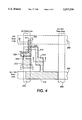
- FIG. 4 is a schematic layout diagram showing semiconductor layers in a cell's circuitry.
- FIG. 5 is a schematic cross section along line a--a in FIG. 4.
- FIG. 6 is a schematic cross section along line b--b in FIG. 4.
- FIG. 7 is a schematic cross section along line c--c in FIG. 4.
- FIG. 8 is a schematic cross section along line d--d in FIG. 4.
- FIG. 9 is a flow chart showing acts in producing cell circuitry as in FIG. 4.
- FIG. 10 is a cross section of a display that includes an array produced as shown in FIG. 9.
- Circuitry or a “circuit” is any physical arrangement of matter that can respond to a first signal at one location or time by providing a second signal at another location or time, where the second signal includes information from the first signal. Circuitry "transfers" a first signal when it receives the first signal at a first location and, in response, provides the second signal at a second location.
- Any two components are “connected” when there is a combination of circuitry that can transfer signals from one of the components to the other.
- two components are “connected” by any combination of connections between them that permits transfer of signals from one of the components to the other.
- Two components are "electrically connected” when there is a combination of circuitry that can transfer electric signals from one to the other. Two components could be electrically connected even though they are not physically connected, such as through a capacitive coupling.
- a “substrate” or “chip” is a unit of material that has a surface at which circuitry can be formed or mounted.
- An “insulating substrate” is a substrate through which no electric current can flow.
- a “layer” is a thickness of material formed over a surface and extending generally parallel to the surface, with one side toward the surface and another side away from the surface.
- a layer may include two or more layers within it, referred to as “sublayers.”
- a layer may be homogeneous or its composition may vary.
- etch is to remove parts of one or more layers of material.
- An “etchant” is a fluid used to etch.
- To perform "physical vapor deposition” is to cause a material to be deposited on a physical structure without a chemical reaction. Examples include sputtering, vacuum evaporation, and e-beam deposition.
- To perform "chemical vapor deposition” is to cause a material to be deposited on a physical structure by use of reactant gases and an energy source to produce a gas-phase chemical reaction.
- the energy source could be thermal, optical, or plasma in nature; "plasma enhanced chemical vapor deposition” uses a plasma energy source.
- An operation "deposits" a layer by depositing material to form the layer, such as by physical or chemical vapor deposition.
- To perform "lithography” is to use a radiation source to transfer a mask pattern to a layer of radiation-sensitive material and then to develop the radiation-sensitive material to obtain a positive or negative copy of the mask pattern.
- the transferred pattern that results from development may be referred to as a "pattern of mask material” if it is to be used for etching.
- An “electric circuit” is a circuit within which components are electrically connected.
- An “electric structure” is a physical structure that includes one or more electric circuits.
- a "thin-film structure” is an electric structure that is formed at a surface of an insulating substrate.
- a thin-film structure could be formed, for example, by deposition and patterned etching of films on the insulating substrate's surface.
- a part of a first layer "covers” or “has a shape that covers” or “is over” a part of a second layer if the part of the second layer is between the part of the first layer and the surface.
- a part of a first layer “extends across” a part of a second layer if the part of the first layer covers the part of the second layer.
- An "integrated circuit” is a circuit formed at a substrate's surface by batch processes such as deposition, lithography, etching, oxidation, diffusion, implantation, annealing, and so forth.
- a “lead” is a part of a component at which the component is electrically connected to other components.
- a “line” is a simple component that extends between and electrically connects two or more leads. A line is “connected between” the components or leads it electrically connects. A lead of a component is “connected” to a lead of another component when the two leads are electrically connected by a combination of leads and lines. In an integrated circuit, leads of two components may also be “connected” by being formed as a single lead that is part of both components.
- An “array” is an article of manufacture that includes an arrangement of "cells.”
- a "two-dimensional array” or “2D array” includes an arrangement of cells in two dimensions.
- a 2D array of circuitry may include rows and columns, with a line for each row and a line for each column. Lines in one direction may be “data lines” through which a cell receives or provides signals that determine or indicate its state. Lines in the other direction may be “scan lines” through which a cell receives a signal enabling it to receive signals from or provide signals to its data line.
- cell circuitry is circuitry connected to a cell's scan line and data line.
- a "crossing region” is a region in which two lines cross, such as a scan line and a data line.
- An “insulating layer” is a layer formed of a non-conductive material.
- a part of a layer "has an edge” if another, complementary part of the layer has been removed by one or more processes, leaving the part of the layer.
- the edge is the boundary between part of a layer and its complementary part.
- a "width" of a part of a layer such as a line is a distance between two edges.
- Edges of two layers or parts of layers in a thin-film structure are "approximately aligned" if their projections onto the surface of the substrate at which the thin-film structure is formed are approximately the same.
- Edges of two layers or parts of layers are "slightly offset" from each other if their projections onto the surface of the substrate are at slightly different positions.
- a component in one layer is "between" edges in another layer if the projection of the component onto the surface of the substrate is between the projections of the edges.
- a "connected shape" in a thin-film structure formed at a surface of a substrate is a part of the structure that is formed from a layer and is bounded by an edge that extends between a first side toward the surface and a second side away from the surface.
- a “channel” is a part of a component through which electric current can flow.
- a channel is "conductive" when the channel is in a state in which current can flow through it.
- a line “includes" a channel when a part of the line is the channel.
- Two channels in a line are "in series" with each other if both must be conductive for the line to be conductive.
- a “channel lead” is a lead that connects to a channel.
- a channel may, for example, extend between two channel leads.
- a “channel region” is a region of an electric structure in which a channel occurs.
- a “charge carrier” is a real or fictitious particle that can transport charge through a channel to produce a current; electrons and holes are examples of charge carriers.
- a “charge carrier source” is an ion, atom, molecule, or other feature of a channel that can provide a charge carrier.
- a “charge carrier destination” is an ion, atom, molecule, or other feature of a channel that can neutralize or stop movement of a charge carrier.
- an "n-channel” is a channel for which the majority of charge carrier sources provide charge carriers of negative sign such as electrons; a “p-channel” is a channel for which the majority of charge carrier sources provide charge carriers of positive sign such as holes.
- Charge carrier sources and destinations are "positioned" so that an event occurs if the densities, types, or other characteristics of the sources and destinations vary with position in a way that causes the event to occur.
- a “dopant” is an ion, atom, molecule, or other particle that can be added to a channel or other part of an integrated circuit during production and that serves as a charge carrier source when the integrated circuit is in use.
- An “n-type dopant” provides charge carriers of negative sign and a “p-type dopant” provides charge carriers of positive sign.
- a process "implants" a dopant if the process causes particles of the dopant to enter a part of an integrated circuit.
- a dopant "dopes" a part of a layer if the dopant is implanted in the part.
- a line is “doped” if it contains an implanted dopant.
- An operation "forms" an electrical connection by producing an electrical structure through which current can flow between components.
- Deposition can form an electrical connection by producing a metal/semiconductor interface or a conductive metal line.
- Doping can form an electrical connection by producing a doped semiconductor line.
- a “transistor” is a component that has a channel that extends between two channel leads, and that also has a third lead-referred to as a "gate lead” or simply “gate”--such that the channel can be switched between high impedance and low impedance by signals that change potential difference between the gate and one of the channel leads, referred to as the "source.”
- the channel lead that is not the source is referred to as the “drain.”
- Other components may have leads called gates, sources, and drains by analogy to transistors.
- Signals on a line control conductivity of a channel if the signals can change conductivity of the channel.
- a line may be called a “gate line” and the signals may be called “gate signals.”
- Two components are electrically connected "under control of" a line if a signal on the line can change conductivity of another line connecting the two components.
- a line that includes a channel can electrically connect two components under control of a gate line.
- a “thin-film transistor” or “TFT” is a transistor that is part of a thin film structure.
- a “capacitive element” is a component that stores a voltage level by storing charge.
- a capacitive element may include two conductive components, called “electrodes,” separated by an insulating layer.
- a cell's area may include a "cell electrode.”
- a cell electrode may serve as one electrode of a capacitor whose other electrode is external to the array.
- An “image” is a pattern of physical light.
- An “image output device” is a device that can provide output defining an image.
- a “display” is an image output device that provides information in a visible form.
- a “liquid crystal cell” is an enclosure containing a liquid crystal material.
- a “liquid crystal display” or “LCD” is a display that includes a liquid crystal cell with a light transmission characteristic that can be controlled in parts of the cell by an array of light control units to cause presentation of an image.
- An “active matrix liquid crystal display” or “AMLCD” is a liquid crystal display that includes a liquid crystal cell and an array of cell circuitry that can cause presentation of an image by the liquid crystal cell.
- FIGS. 1-3 show general features of the invention.
- FIG. 1 shows schematically functions in forming an M ⁇ N array in which a cell's circuitry includes a semiconductor line that is connected to a metal scan line and that crosses another semiconductor line at a channel between connections to a data line and a data lead.
- FIG. 2 shows general acts in implementing the functions shown in FIG. 1.
- FIG. 3 shows other general acts in implementing the functions shown in FIG. 1.
- Array 10 in FIG. 1 includes M scan lines, from first scan line 20 through Mth scan line 22, and N data lines, from first data line 24 through Nth data line 26.
- Cell circuitry connected to mth scan line 30 and nth data line 32 is illustratively shown in more detail.
- array 10 can be produced by performing a number of functions.
- One function, designated “A,” forms mth scan line 30 and the other scan lines, each of which includes metal.
- Another function is to produce cell circuitry for each crossing region.
- This function produces component 40, which has a data lead for receiving signals from or providing signals to nth data line 32.
- component 40 which has a data lead for receiving signals from or providing signals to nth data line 32.
- C1 one part of this function, designated "C1” forms semiconductor line 42 connected between nth data line 32 and a data lead of component 40.
- C2 Another part of this function, designated “C2,” forms semiconductor line 44 which is conductive and which crosses semiconductor line 42 at channel 46.
- Another function is to form electrical connections at appropriate connecting points.
- One part of this function designated “D1,” forms an electrical connection between nth data line 32 and semiconductor line 42.
- a second part of this function designated “D2,” forms an electrical connection between semiconductor line 42 and the data lead of component 40.
- a third part of this function designated “D3,” forms an electrical connection between mth scan line 30 and semiconductor line 44. Because of these connections, signals on mth scan line 30 control conductivity of channel 46.
- FIG. 1 could be implemented in many ways using various techniques for producing circuitry on a substrate.
- FIG. 2 shows a sequence of general acts that can implement the functions in FIG. 1.
- the act in box 60 deposits and lithographically patterns a first semiconductor layer, producing semiconductor line 42 in FIG. 1.
- the act in box 60 can also produce the data lead and other parts of component 40, such as a capacitor electrode.
- the act in box 62 deposits a first insulating layer over the pattern from box 60. Then, the act in box 64 deposits and lithographically patterns a second semiconductor layer, producing semiconductor line 44 in FIG. 1.
- the act in box 66 then implants a dopant. Because semiconductor line 44 crosses channel 46, channel 46 is shielded from the dopant, but other parts of semiconductor line 42 are doped, forming channel leads for channel 46. The act in box 66 can therefore form an electrical connection between semiconductor line 42 and the data lead of component 40, the function designated D2 in FIG. 1.
- the act in box 70 deposits and lithographically patterns a scan line layer that includes metal, producing M scan lines 20 through 22.
- the act in box 70 therefore forms an electrical connection between semiconductor line 44 and mth scan line 30, by forming a metal/semiconductor interface.
- the act in box 72 deposits a second insulating layer.
- the act in box 74 then lithographically forms openings in the first and second insulating layers to expose the connecting point at which semiconductor line 42 connects to nth data line 32.
- the act in box 76 then deposits and lithographically patterns a data line layer, producing N data lines 24 through 26.
- the act in box 76 therefore forms an electrical connection between semiconductor line 42 and nth data line 32, because the metal in the opening formed in box 74 forms a metal/semiconductor interface.
- FIG. 3 shows another sequence of general acts that could be used implement the functions in FIG. 1.
- the sequence in FIG. 3 would produce a structure with a gate under a channel and with a top ITO layer, resembling the structure disclosed in copending, coassigned U.S. patent application No. 08/235,009, entitled "Electrically Isolated Pixel Element in a Low Voltage Activated Active Matrix Liquid Crystal Display and Method," incorporated herein by reference.
- the act in box 100 deposits and lithographically patterns a scan line layer, producing scan lines.
- the act in box 102 then deposits and lithographically patterns a layer referred to as the "second semiconductor layer" because it includes a line that serves the same function as semiconductor line 44 in FIG. 1. Deposition of the second semiconductor layer on a scan line forms a metal/semiconductor interface, forming an electrical connection.
- the act in box 104 deposits a first insulating layer over the pattern from box 102. Then, the act in box 106 deposits a layer referred to as the "first semiconductor layer" because it is subsequently etched to form a pattern that includes a line that serves the same function as semiconductor line 42 in FIG. 1.
- the act in box 110 deposits a second insulating layer over the first semiconductor layer from box 106. Then, the act in box 112 performs a self-aligned back side exposure followed by an etch to lithographically pattern the second insulating layer so that it includes an island over the channel in the first semiconductor layer. The act in box 114 then implants a dopant, with the channel shielded from the dopant by the island from box 112. The act in box 114 can also anneal to activate the channel and passivate.
- the act in box 116 then lithographically patterns the first semiconductor layer, producing a line that serves the same function as semiconductor line 42 in FIG. 1.
- the act in box 116 can also produce the data lead and other parts of component 40, such as a capacitor electrode, as in box 60 in FIG. 2.
- the act in box 120 then deposits and lithographically patterns a third insulating layer so that it has openings to the first semiconductor layer at the connection points.
- the act in box 122 then deposits and lithographically patterns a data line layer, producing data lines.
- the act in box 122 therefore forms an electrical connection between the line in the first semiconductor layer and a data line, because the metal in the opening formed in box 120 forms a metal/semiconductor interface.
- FIGS. 4-8 illustrate cell circuitry.
- FIG. 4 shows a layout of first and second semiconductor layers.
- FIGS. 5-8 show representative cross sections of cell circuitry in FIG. 4, along lines a--a, b--b, c--c, and d--d, respectively.
- FIG. 4 shows a part of an M ⁇ N array, with mth scan line 200, (m+1)th scan line 202, nth data line 204, and (n+1)th data line 206 in dashed lines.
- FIG. 4 also shows part of the cell circuitry for the cell that is connected to mth scan line 200 and nth data line 204.
- the cell's circuitry includes first semiconductor pattern 210, with a line that extends from first connecting point 212 to second connecting point 214 and with another line extending from second connecting point 214 to capacitor electrode 216.
- First connecting point 212 is substantially all within the edges of nth data line 204, to which it is electrically connected.
- the edges of capacitor electrode 216 are aligned with the edges of (m+1)th scan line 202, forming a capacitive element.
- the cell's circuitry also includes second semiconductor pattern 220, a line that crosses first semiconductor pattern 210 at channels 222 and 224. Second semiconductor pattern 220 extends from end 226, at which it is electrically connected to mth scan line 200.
- the layout in FIG. 4 is designed to have the following dimensions when implemented with poly-Si TFTs on an insulating substrate: Each cell is 30 ⁇ m ⁇ 30 ⁇ m, of which the scan line occupies 6 ⁇ m and the data line occupies 5 ⁇ m.
- the lines in first semiconductor pattern 210 are 2 ⁇ m wide, and second semiconductor pattern 220 is 2.5 ⁇ m wide. In general, the smallest features are 2 ⁇ m and the smallest separations are 3 ⁇ m, with 1.0 ⁇ m overlay and an aperture ratio of 49.7%.
- the cell circuitry in FIG. 4 is designed so that the capacitive element formed by (m+1)th scan line 202 and capacitor electrode 216 has sufficient capacitance that stored voltages are not significantly affected by capacitive coupling with data line voltage fluctuations. Dark matrix is used to improve image quality by blocking stray illumination, as at edges, with minimum sacrifice of aperture.
- FIG. 5 shows substrate 240, which can be quartz, with surface 242 at which circuitry 244 is formed.
- Circuitry 244 includes insulating layer 250 on surface 242, on which capacitor electrodes 252 and 254 are formed for the cell circuitry connected to the (m-1)th scan line and to the nth and (n-1)th data lines respectively.
- Capacitor electrodes 252 and 254 each include heavily n-doped poly-Si, as indicated by "n+,” except that a small area of electrode 252 that is under second semiconductor pattern 220 is undoped, intrinsic poly-Si, as indicated by "i.” If the area in which second semiconductor pattern 220 overlaps capacitor electrode 252 is small, as in FIG. 4, this small undoped area has an insignificant effect on capacitance.
- Circuitry 244 also includes insulating layer 256 between capacitor electrodes 252 and 254 and second semiconductor pattern 220 shown in FIG. 4.
- Second semiconductor pattern 220 also includes heavily n-doped poly-Si, and is electrically connected to mth scan line 200, which includes aluminum, and which can be implemented as a hybrid TiW/AlCu stack. Because of the small overlap with second semiconductor pattern 220 and because of a slight dip between capacitor electrodes 252 and 254, mth scan line has slight variations in cross section, but in general its section remains substantially uniform across the array.
- Circuitry 244 then includes insulating layer 260 separating mth scan line 200 from nth data line 204, which can also be implemented as a hybrid TiW/AlCu stack. Over nth data line 204 is passivation layer 262 of polyimide.
- FIG. 6 shows a different cross section of circuitry 244, with many of the same features as FIG. 5, but also showing channel 224 in first semiconductor pattern 210.
- second semiconductor pattern 220 provides signals from mth scan line 200 to channel region 270, controlling conductivity of channel 224.
- FIG. 7 shows a cross section through first connecting point 212.
- nth data line 204 forms a metal/semiconductor contact with first semiconductor pattern 210 through an opening in insulating layers 256 and 260.
- Dark matrix lines 280 and 282 are formed on passivation layer 262 over the edges of nth data line 204, and indium tin oxide (ITO) pixel electrodes 290 and 292 slightly overlap dark matrix lines 280 and 282.
- ITO indium tin oxide
- FIG. 8 shows a cross section through second connecting point 214.
- Metal pattern 300 forms a metal/semiconductor contact with first semiconductor pattern 210 through an opening in insulating layers 256 and 260.
- Metal pattern 300 can be formed from the same metal layer as nth data line 204.
- Conductive dark matrix pattern 302 can be formed from the same material as dark matrix lines 280 and 282 in FIG. 7.
- ITO pixel electrode 290 then forms an electrical connection with second connecting point 214 through metal pattern 300 and dark matrix pattern 302.
- metal pattern 300 blocks stray illumination at the edges of insulating layers 256 and 260 and smooths the topology
- dark matrix pattern 302 provides process compatibility between ITO pixel electrode 290 and metal pattern 300.
- FIG. 9 shows acts in producing cell circuitry as described above.
- the act in box 330 begins by preparing a surface of a quartz substrate.
- the act in box 330 can include any necessary cleaning.
- the act in box 332 then deposits a first layer of low temperature oxide (LTO), which can be SiO 2 deposited with plasma chemical vapor deposition.
- LTO low temperature oxide
- the first LTO layer can be deposited to a thickness of 0.7 ⁇ m and then annealed.
- the act in box 334 deposits a layer of a-Si to a thickness of 0.1 ⁇ m, then performs Si self-ion implantation to enhance performance.
- the act in box 334 also performs crystallization and annealing at 600° C. As a result, the a-Si becomes poly-Si.
- the act in box 334 performs lithography to produce a pattern of mask material that covers the parts of the poly-Si that form first semiconductor pattern 210. Then, the act in box 334 etches to remove areas not covered by the pattern of mask material, leaving first semiconductor pattern 210.
- the act in box 336 deposits a second layer of LTO to a thickness of 0.085 ⁇ m.
- the act in box 336 also performs oxidation at 950° C. under 150 atmospheres and anneals the second LTO layer.
- the act in box 340 deposits a layer of poly-Si to a thickness of 0.35 ⁇ m.
- the act in box 340 performs lithography to produce a pattern of mask material that covers the parts of the poly-Si that form second semiconductor pattern 220 or another similar pattern that crosses the first semiconductor pattern at one or two channels. Then, the act in box 340 etches to remove areas not covered by the pattern of mask material, leaving second semiconductor pattern 220. Then, the act in box 340 removes the mask material.
- the act in box 342 performs lithography to produce a pattern of mask material that does not cover the cell circuitry, but may, for example, cover areas in which peripheral circuitry is being formed on the substrate.
- the act in box 342 then implants a heavy concentration of an n-type dopant, making second semiconductor pattern 220 conductive and forming conductive leads in first semiconductor pattern 210.
- the act in box 342 removes the mask material by an appropriate plasma resist etching.
- the act in box 344 similarly performs lithography to produce a pattern of mask material that does not cover the peripheral circuitry, but covers the cell circuitry.
- the act in box 344 then implants a heavy concentration of a p-type dopant to form conductive areas in the peripheral circuitry. Then, the act in box 344 removes the mask material.
- the act in box 344 can also perform crystallization annealing at 600° C.
- the acts in boxes 342 and 344 may employ any of a number of implantation processes, including non-mass selection processes such as ion showering, plasma extraction, ion bucket, and so forth.
- the act in box 346 deposits a layer of metal to a thickness of 0.1-0.2 ⁇ m to produce a scan line layer.
- the scan line layer can, for example, be a hybrid TiW/AlCu multilayer stack with three or four layers of 0.01 ⁇ m of TiW separated by two or three layers of 0.05 of AlCu, similar to the multilayer metal lines described in copending, coassigned U.S. patent application No. 08/234,897, now issued as U.S. Pat. No. 5,518,805, entitled "Hillock-Free Multilayer Metal Lines for High Performance Thin Film Structures," incorporated herein by reference.
- the hybrid films can be sputtered or evaporated using two alloy targets, alternating between the targets.
- These thicknesses avoid hillock formation in the AlCu layers during processing, yet provide a thin barrier metal to avoid intermixing between the AlCu layers or between an AlCu layer and other layers, avoiding hillock formation, film bubbling, peeling, or spiking into a poly-Si layer, for example.
- the films can all be wet etched at approximately the same rate to achieve a high degree of dimension control.
- the ratio of the wet TiW etchant to the wet AlCu etchant can be approximately 50:1; in contrast to the standard Al etchant, this mixed etchant is much lower in viscosity and less violent during etching, removing bubbling.
- the act in box 346 then performs lithography to produce a pattern of mask material that covers the parts of the scan line layer that form the scan lines. Then, the act in box 346 etches to remove areas not covered by the pattern of mask material, leaving the scan lines. Then, the act in box 346 removes the mask material.
- the act in box 350 deposits a third layer of LTO to a thickness of 0.7 ⁇ m.
- the act in box 350 also performs hydrogenation to passivate the channels in first semiconductor pattern 210 and an appropriate wet oxide etch to remove the damaged layer resulting from the hydrogenation process. This hydrogenation does not cause degradation of channels in first semiconductor pattern 210 because the scan lines formed in box 346 are not over the channels in first semiconductor pattern 210.
- the act in box 352 performs lithography to produce a pattern of mask material that does not cover first and second connection points 212 and 214 and any other areas in which metal in the data line layer contacts the layer formed in box 334, but covers all other areas.
- the act in box 352 then etches to form openings in the second and third LTO layers from boxes 336 and 350 in the areas that are not covered. Then, the act in box 352 removes the mask material.
- the act in box 354 deposits a data metal layer to a thickness of 0.5 ⁇ m.
- the data metal layer can, for example, be a hybrid TiW/AlCu multilayer stack as described above.
- the act in box 354 then performs lithography to produce a pattern of mask material that covers the parts of the data line layer that form the data lines and that cover the opening to second connection point 214. Then, the act in box 354 etches to remove areas not covered by the pattern of mask material, leaving the data lines. Then, the act in box 354 removes the mask material.
- the data line layer over second connection point 214 blocks light leakage due to poor liquid crystal control as a result of the steepness of the topology. This light leakage blocking raises contrast ratio dramatically.
- the act in box 356 deposits a passivation layer of polyimide to a thickness of 1.5 ⁇ m.
- the act in box 356 performs lithography to produce a pattern of mask material that does not cover second connection point 214 and any other areas in which metal in the data line layer should be exposed for contact.
- the act in box 356 then etches to form openings in the passivation layer in the areas that are not covered. Then, the act in box 356 removes the mask material.
- the passivation layer also acts to planarize the surface, and spin-on glass could be used instead of polyimide. Planarization is important because of the steepness of the topology.
- the act in box 360 deposits a dark matrix layer of TiW to a thickness of 0.1 ⁇ m.
- TiW is advantageous as a dark matrix material because it acts as a mutual etch stop with indium-tin-oxide (ITO) and aluminum and has a high optical density even in a thin layer, and it is advantageously applied over the circuitry rather than on a cover sheet.
- the act in box 360 performs lithography to produce a pattern of mask material that covers the dark matrix layer only in areas in which light shielding is needed, such as along the edges of each data line and around second connection point 214.
- the act in box 360 then etches to remove the areas that are not covered. Then, the act in box 360 removes the mask material.
- the act in box 362 deposits ITO to a thickness of 0.055 ⁇ m.
- the act in box 362 performs lithography to produce a pattern of mask material that covers the ITO layer in light transmissive cell areas.
- the act in box 362 then etches to remove the areas that are not covered.
- Them the act in box 362 removes the mask material and anneals the ITO layer at 280° C.
- FIG. 10 shows features of a display that includes circuitry produced as described above.
- Display 400 in FIG. 10 includes array substrate 402 and cover substrate 404.
- Array substrate 402 is quartz, but cover substrate 404 could be quartz or glass.
- Circuitry 410 formed at surface 412 of array substrate 402 includes array circuitry 414 and peripheral circuitry 416.
- Peripheral circuitry 416 is outside the boundary of array circuitry 414, and can include drivers connected to the ends of scan lines and data lines.
- array circuitry 414 can have n-doped poly-Si TFTs
- peripheral circuitry 416 can have p-doped poly-Si TFTs.
- ITO layer 420 is formed at a surface of cover substrate 404 and faces surface 412 of array substrate 402, separated by spacers 422 and 424 at the boundary of array circuitry 414. If display 400 is a projection device, it should be small enough that no other spacers are needed within the boundary of array circuitry 414, because spacers can cause image problems in a projection display. The need for spacers can be reduced by using thicker substrates and by assembling at lower temperatures.
- Display 400 also includes liquid crystal material 430 in the cavity defined by ITO layer 420, array circuitry 414, and spacers 422 and 424.
- Liquid crystal material 430 can be a 90° twisted nematic liquid crystal.
- Display 400 could, for example, be a wafer-scale projection display of approximately 1.5" diagonal. Display 400 could alternatively be a large area direct viewing display.
- Display 400 can be assembled using techniques like those described in copending, coassigned U.S. patent application No. 08/235,011, now issued as U.S. Pat. No. 5,491,347, entitled "Thin-Film Structure with Dense Array of Binary Control Units for Presenting Images,” incorporated herein by reference.
- a dummy 30 ⁇ 30 array of cells with no liquid crystal assembly has been manufactured, tested, and found to be fully functional.
- the implementation described above provides thin film circuitry on an insulating substrate.
- the invention could be implemented with other types of circuitry on other types of substrates.
- circuitry with specific geometric and electric characteristics, but the invention could be implemented with different geometries and with different circuitry.
- the implementation described above includes layers of specified thicknesses, produced from specified materials by specified processes, but other thicknesses could be produced, and other materials and processes could be used, such as thinner semiconductor and gate oxide layers to improve TFT performance or to increase storage capacitance.
- other semiconductor materials could be used in the semiconductor layers, including but not limited to a-Si, SiGe, CdSe, or a composite layer of poly-Si and SiGe.
- various conductive materials could be used in the scan lines and data lines, including but not limited to ITO, MoTa, Cr, MoCr, Ta, Cu, Ti, TiN, and organic conductive materials.
- the invention could be applied in many ways, including arrays for displays, sensors, and light valves.
Abstract
Description
Claims (22)
Priority Applications (4)
| Application Number | Priority Date | Filing Date | Title |
|---|---|---|---|
| US08/367,983 US5557534A (en) | 1995-01-03 | 1995-01-03 | Forming array with metal scan lines to control semiconductor gate lines |
| JP34298895A JPH08236779A (en) | 1995-01-03 | 1995-12-28 | Method of forming array circuit on surface of substrate |
| EP96300050A EP0721215B1 (en) | 1995-01-03 | 1996-01-03 | Forming array with metal scan lines to control semiconductor gatelines |
| DE69633533T DE69633533T2 (en) | 1995-01-03 | 1996-01-03 | Production of a grid with metallic scanning lines for the control of semiconductor grid lines |
Applications Claiming Priority (1)
| Application Number | Priority Date | Filing Date | Title |
|---|---|---|---|
| US08/367,983 US5557534A (en) | 1995-01-03 | 1995-01-03 | Forming array with metal scan lines to control semiconductor gate lines |
Publications (1)
| Publication Number | Publication Date |
|---|---|
| US5557534A true US5557534A (en) | 1996-09-17 |
Family
ID=23449403
Family Applications (1)
| Application Number | Title | Priority Date | Filing Date |
|---|---|---|---|
| US08/367,983 Expired - Lifetime US5557534A (en) | 1995-01-03 | 1995-01-03 | Forming array with metal scan lines to control semiconductor gate lines |
Country Status (4)
| Country | Link |
|---|---|
| US (1) | US5557534A (en) |
| EP (1) | EP0721215B1 (en) |
| JP (1) | JPH08236779A (en) |
| DE (1) | DE69633533T2 (en) |
Cited By (18)
| Publication number | Priority date | Publication date | Assignee | Title |
|---|---|---|---|---|
| US5608245A (en) * | 1995-12-21 | 1997-03-04 | Xerox Corporation | Array on substrate with repair line crossing lines in the array |
| US5648674A (en) * | 1995-06-07 | 1997-07-15 | Xerox Corporation | Array circuitry with conductive lines, contact leads, and storage capacitor electrode all formed in layer that includes highly conductive metal |
| US5693567A (en) * | 1995-06-07 | 1997-12-02 | Xerox Corporation | Separately etching insulating layer for contacts within array and for peripheral pads |
| US5703382A (en) * | 1995-11-20 | 1997-12-30 | Xerox Corporation | Array having multiple channel structures with continuously doped interchannel regions |
| US5770871A (en) * | 1996-06-20 | 1998-06-23 | Xerox Corporation | Sensor array with anticoupling layer between data lines and charge collection electrodes |
| US5782665A (en) * | 1995-12-29 | 1998-07-21 | Xerox Corporation | Fabricating array with storage capacitor between cell electrode and dark matrix |
| US6040812A (en) * | 1996-06-19 | 2000-03-21 | Xerox Corporation | Active matrix display with integrated drive circuitry |
| US6051446A (en) * | 1998-04-09 | 2000-04-18 | National Semiconductor Corporation | Thin liquid crystal transducer pixel cell having self-aligned support pillars |
| US6097466A (en) * | 1997-11-18 | 2000-08-01 | Sanyo Electric Co., Ltd. | Reflection type liquid crystal display |
| US6137558A (en) * | 1997-11-18 | 2000-10-24 | Sanyo Electric Co., Ltd. | Active-matrix liquid crystal display |
| US6188456B1 (en) | 1997-11-18 | 2001-02-13 | Sanyo Electric Co., Ltd. | Liquid crystal display and projector using the same |
| US6281891B1 (en) | 1995-06-02 | 2001-08-28 | Xerox Corporation | Display with array and multiplexer on substrate and with attached digital-to-analog converter integrated circuit having many outputs |
| US20020154235A1 (en) * | 2000-12-29 | 2002-10-24 | Kim Ik Soo | X-ray detecting device and fabricating method thereof |
| US6487712B1 (en) * | 1999-10-25 | 2002-11-26 | Dongbu Electronics Co., Ltd. | Method of manufacturing mask for conductive wirings in semiconductor device |
| US6569595B1 (en) * | 1999-02-25 | 2003-05-27 | Kabushiki Kaisha Toshiba | Method of forming a pattern |
| US6683333B2 (en) * | 2000-07-14 | 2004-01-27 | E Ink Corporation | Fabrication of electronic circuit elements using unpatterned semiconductor layers |
| US20090108304A1 (en) * | 2007-10-26 | 2009-04-30 | Tse Nga Ng | Protecting semiconducting oxides |
| US7617465B1 (en) * | 2004-09-16 | 2009-11-10 | Cadence Design Systems, Inc. | Method and mechanism for performing latch-up check on an IC design |
Citations (18)
| Publication number | Priority date | Publication date | Assignee | Title |
|---|---|---|---|---|
| US4059461A (en) * | 1975-12-10 | 1977-11-22 | Massachusetts Institute Of Technology | Method for improving the crystallinity of semiconductor films by laser beam scanning and the products thereof |
| US4691434A (en) * | 1982-02-19 | 1987-09-08 | Lasarray Holding Ag | Method of making electrically conductive regions in monolithic semiconductor devices as applied to a semiconductor device |
| US5060045A (en) * | 1988-10-17 | 1991-10-22 | Hitachi, Ltd. | Semiconductor integrated circuit device and method of manufacturing the same |
| US5075753A (en) * | 1988-12-27 | 1991-12-24 | Hitachi, Ltd. | Semiconductor integrated circuit device |
| US5243208A (en) * | 1987-05-27 | 1993-09-07 | Hitachi, Ltd. | Semiconductor integrated circuit device having a gate array with a ram and by-pass signal lines which interconnect a logic section and I/O unit circuit of the gate array |
| US5291043A (en) * | 1990-02-07 | 1994-03-01 | Mitsubishi Denki Kabushiki Kaisha | Semiconductor integrated circuit device having gate array |
| US5324674A (en) * | 1992-04-02 | 1994-06-28 | General Electric Company | Fabrication method for a self-aligned thin film transistor having reduced end leakage and device formed thereby |
| US5346833A (en) * | 1993-04-05 | 1994-09-13 | Industrial Technology Research Institute | Simplified method of making active matrix liquid crystal display |
| US5348902A (en) * | 1992-01-21 | 1994-09-20 | Hitachi, Ltd. | Method of designing cells applicable to different design automation systems |
| US5367187A (en) * | 1992-12-22 | 1994-11-22 | Quality Semiconductor, Inc. | Master slice gate array integrated circuits with basic cells adaptable for both input/output and logic functions |
| US5369595A (en) * | 1988-03-18 | 1994-11-29 | International Business Machines Corporation | Method of combining gate array and standard cell circuits on a common semiconductor chip |
| US5369596A (en) * | 1990-11-22 | 1994-11-29 | Kabushiki Kaisha Toshiba | Semiconductor integrated circuit fabrication method |
| US5388055A (en) * | 1990-09-07 | 1995-02-07 | Fujitsu Limited | Semiconductor integrated circuit having polycell structure and method of designing the same |
| US5391507A (en) * | 1993-09-03 | 1995-02-21 | General Electric Company | Lift-off fabrication method for self-aligned thin film transistors |
| US5412493A (en) * | 1992-09-25 | 1995-05-02 | Sony Corporation | Liquid crystal display device having LDD structure type thin film transistors connected in series |
| US5414547A (en) * | 1991-11-29 | 1995-05-09 | Seiko Epson Corporation | Liquid crystal display device and manufacturing method therefor |
| US5424857A (en) * | 1993-06-22 | 1995-06-13 | Asahi Glass Company Ltd. | Matrix-type display apparatus with conductor wire interconnecting capacitor electrodes |
| US5491347A (en) * | 1994-04-28 | 1996-02-13 | Xerox Corporation | Thin-film structure with dense array of binary control units for presenting images |
Family Cites Families (4)
| Publication number | Priority date | Publication date | Assignee | Title |
|---|---|---|---|---|
| JPH0656461B2 (en) * | 1982-05-06 | 1994-07-27 | セイコーエプソン株式会社 | Matrix array |
| US5365079A (en) * | 1982-04-30 | 1994-11-15 | Seiko Epson Corporation | Thin film transistor and display device including same |
| FR2662290B1 (en) * | 1990-05-15 | 1992-07-24 | France Telecom | METHOD FOR PRODUCING A DISPLAY SCREEN WITH ACTIVE MATRIX AND STORAGE CAPACITORS AND SCREEN OBTAINED BY THIS PROCESS. |
| JP3024661B2 (en) * | 1990-11-09 | 2000-03-21 | セイコーエプソン株式会社 | Active matrix substrate and manufacturing method thereof |
-
1995
- 1995-01-03 US US08/367,983 patent/US5557534A/en not_active Expired - Lifetime
- 1995-12-28 JP JP34298895A patent/JPH08236779A/en active Pending
-
1996
- 1996-01-03 EP EP96300050A patent/EP0721215B1/en not_active Expired - Lifetime
- 1996-01-03 DE DE69633533T patent/DE69633533T2/en not_active Expired - Lifetime
Patent Citations (18)
| Publication number | Priority date | Publication date | Assignee | Title |
|---|---|---|---|---|
| US4059461A (en) * | 1975-12-10 | 1977-11-22 | Massachusetts Institute Of Technology | Method for improving the crystallinity of semiconductor films by laser beam scanning and the products thereof |
| US4691434A (en) * | 1982-02-19 | 1987-09-08 | Lasarray Holding Ag | Method of making electrically conductive regions in monolithic semiconductor devices as applied to a semiconductor device |
| US5243208A (en) * | 1987-05-27 | 1993-09-07 | Hitachi, Ltd. | Semiconductor integrated circuit device having a gate array with a ram and by-pass signal lines which interconnect a logic section and I/O unit circuit of the gate array |
| US5369595A (en) * | 1988-03-18 | 1994-11-29 | International Business Machines Corporation | Method of combining gate array and standard cell circuits on a common semiconductor chip |
| US5060045A (en) * | 1988-10-17 | 1991-10-22 | Hitachi, Ltd. | Semiconductor integrated circuit device and method of manufacturing the same |
| US5075753A (en) * | 1988-12-27 | 1991-12-24 | Hitachi, Ltd. | Semiconductor integrated circuit device |
| US5291043A (en) * | 1990-02-07 | 1994-03-01 | Mitsubishi Denki Kabushiki Kaisha | Semiconductor integrated circuit device having gate array |
| US5388055A (en) * | 1990-09-07 | 1995-02-07 | Fujitsu Limited | Semiconductor integrated circuit having polycell structure and method of designing the same |
| US5369596A (en) * | 1990-11-22 | 1994-11-29 | Kabushiki Kaisha Toshiba | Semiconductor integrated circuit fabrication method |
| US5414547A (en) * | 1991-11-29 | 1995-05-09 | Seiko Epson Corporation | Liquid crystal display device and manufacturing method therefor |
| US5348902A (en) * | 1992-01-21 | 1994-09-20 | Hitachi, Ltd. | Method of designing cells applicable to different design automation systems |
| US5324674A (en) * | 1992-04-02 | 1994-06-28 | General Electric Company | Fabrication method for a self-aligned thin film transistor having reduced end leakage and device formed thereby |
| US5412493A (en) * | 1992-09-25 | 1995-05-02 | Sony Corporation | Liquid crystal display device having LDD structure type thin film transistors connected in series |
| US5367187A (en) * | 1992-12-22 | 1994-11-22 | Quality Semiconductor, Inc. | Master slice gate array integrated circuits with basic cells adaptable for both input/output and logic functions |
| US5346833A (en) * | 1993-04-05 | 1994-09-13 | Industrial Technology Research Institute | Simplified method of making active matrix liquid crystal display |
| US5424857A (en) * | 1993-06-22 | 1995-06-13 | Asahi Glass Company Ltd. | Matrix-type display apparatus with conductor wire interconnecting capacitor electrodes |
| US5391507A (en) * | 1993-09-03 | 1995-02-21 | General Electric Company | Lift-off fabrication method for self-aligned thin film transistors |
| US5491347A (en) * | 1994-04-28 | 1996-02-13 | Xerox Corporation | Thin-film structure with dense array of binary control units for presenting images |
Non-Patent Citations (10)
| Title |
|---|
| Lewis, A., and Wu, I W., Polysilicon TFTs for Active Matrix Liquid Crystal Displays, IEICE Transactions, vol.J76 C II, No. 5, May 1993, pp. 211 226. * |
| Lewis, A., and Wu, I-W., "Polysilicon TFTs for Active Matrix Liquid Crystal Displays," IEICE Transactions, vol.J76-C-II, No. 5, May 1993, pp. 211-226. |
| Martin, R., Chuang, T., Steemers, H., Allen, R., Fulks, R., Stuber, S., Lee, D., Young, M., Ho, J., Nguyen, M., Meuli, W., Fiske, T., Bruce, R., Thompson, M., Tilton, M., and Silverstein, L. D., "P-70: A 6.3-Mpixel AMLCD," SID 93 Digest, 1993, pp. 704-707. |
| Martin, R., Chuang, T., Steemers, H., Allen, R., Fulks, R., Stuber, S., Lee, D., Young, M., Ho, J., Nguyen, M., Meuli, W., Fiske, T., Bruce, R., Thompson, M., Tilton, M., and Silverstein, L. D., P 70: A 6.3 Mpixel AMLCD, SID 93 Digest , 1993, pp. 704 707. * |
| Wu, I W., High definition displays and tecnhology trends in TFT LCDs, Journal of the SID , vol. 2, No. 1, 1994, pp. 1 14. * |
| Wu, I W., Stuber, S., Tsai, C. C., Yao W., Lewis, A., Fulks, R., Chiang, A., and Thompson, M., Processing and Device Performance of Low Temperature CMOS Poly TFTs on 18.4 in. Diagonal Substrates for AMLCD Application, SID 92 Digest , 1992, pp. 615 618. * |
| Wu, I-W., "High-definition displays and tecnhology trends in TFT-LCDs," Journal of the SID, vol. 2, No. 1, 1994, pp. 1-14. |
| Wu, I-W., Stuber, S., Tsai, C. C., Yao W., Lewis, A., Fulks, R., Chiang, A., and Thompson, M., "Processing and Device Performance of Low-Temperature CMOS Poly-TFTs on 18.4-in.-Diagonal Substrates for AMLCD Application," SID 92 Digest, 1992, pp. 615-618. |
| Wu. I W., Polycrystalline Silicon Thin Film Transistors for Liquid Crystal Displays, Solid State Phenomena , vols. 37 38, 1944, pp. 553 564. * |
| Wu. I-W., "Polycrystalline Silicon Thin Film Transistors for Liquid Crystal Displays," Solid State Phenomena, vols. 37-38, 1944, pp. 553-564. |
Cited By (23)
| Publication number | Priority date | Publication date | Assignee | Title |
|---|---|---|---|---|
| US6281891B1 (en) | 1995-06-02 | 2001-08-28 | Xerox Corporation | Display with array and multiplexer on substrate and with attached digital-to-analog converter integrated circuit having many outputs |
| US5648674A (en) * | 1995-06-07 | 1997-07-15 | Xerox Corporation | Array circuitry with conductive lines, contact leads, and storage capacitor electrode all formed in layer that includes highly conductive metal |
| US5693567A (en) * | 1995-06-07 | 1997-12-02 | Xerox Corporation | Separately etching insulating layer for contacts within array and for peripheral pads |
| US5703382A (en) * | 1995-11-20 | 1997-12-30 | Xerox Corporation | Array having multiple channel structures with continuously doped interchannel regions |
| US5608245A (en) * | 1995-12-21 | 1997-03-04 | Xerox Corporation | Array on substrate with repair line crossing lines in the array |
| US5782665A (en) * | 1995-12-29 | 1998-07-21 | Xerox Corporation | Fabricating array with storage capacitor between cell electrode and dark matrix |
| US6040812A (en) * | 1996-06-19 | 2000-03-21 | Xerox Corporation | Active matrix display with integrated drive circuitry |
| US5770871A (en) * | 1996-06-20 | 1998-06-23 | Xerox Corporation | Sensor array with anticoupling layer between data lines and charge collection electrodes |
| US6188456B1 (en) | 1997-11-18 | 2001-02-13 | Sanyo Electric Co., Ltd. | Liquid crystal display and projector using the same |
| US6556267B2 (en) | 1997-11-18 | 2003-04-29 | Sanyo Electric Co., Ltd. | Liquid crystal display and projector using the same |
| US6097466A (en) * | 1997-11-18 | 2000-08-01 | Sanyo Electric Co., Ltd. | Reflection type liquid crystal display |
| US6137558A (en) * | 1997-11-18 | 2000-10-24 | Sanyo Electric Co., Ltd. | Active-matrix liquid crystal display |
| US6292247B1 (en) * | 1997-11-18 | 2001-09-18 | Sanyo Electric Co., Ltd. | Active-matrix liquid crystal display |
| US6051446A (en) * | 1998-04-09 | 2000-04-18 | National Semiconductor Corporation | Thin liquid crystal transducer pixel cell having self-aligned support pillars |
| US6569595B1 (en) * | 1999-02-25 | 2003-05-27 | Kabushiki Kaisha Toshiba | Method of forming a pattern |
| US6487712B1 (en) * | 1999-10-25 | 2002-11-26 | Dongbu Electronics Co., Ltd. | Method of manufacturing mask for conductive wirings in semiconductor device |
| US6683333B2 (en) * | 2000-07-14 | 2004-01-27 | E Ink Corporation | Fabrication of electronic circuit elements using unpatterned semiconductor layers |
| US20020154235A1 (en) * | 2000-12-29 | 2002-10-24 | Kim Ik Soo | X-ray detecting device and fabricating method thereof |
| US7402810B2 (en) * | 2000-12-29 | 2008-07-22 | Lg Display Co., Ltd. | X-ray detecting device and fabricating method thereof |
| US7617465B1 (en) * | 2004-09-16 | 2009-11-10 | Cadence Design Systems, Inc. | Method and mechanism for performing latch-up check on an IC design |
| US20090108304A1 (en) * | 2007-10-26 | 2009-04-30 | Tse Nga Ng | Protecting semiconducting oxides |
| US8258021B2 (en) | 2007-10-26 | 2012-09-04 | Palo Alto Research Center Incorporated | Protecting semiconducting oxides |
| US8497506B2 (en) | 2007-10-26 | 2013-07-30 | Palo Alto Research Center Incorporated | Protecting semiconducting oxides |
Also Published As
| Publication number | Publication date |
|---|---|
| DE69633533T2 (en) | 2005-01-27 |
| DE69633533D1 (en) | 2004-11-11 |
| JPH08236779A (en) | 1996-09-13 |
| EP0721215B1 (en) | 2004-10-06 |
| EP0721215A2 (en) | 1996-07-10 |
| EP0721215A3 (en) | 1998-06-03 |
Similar Documents
| Publication | Publication Date | Title |
|---|---|---|
| US5557534A (en) | Forming array with metal scan lines to control semiconductor gate lines | |
| US5648674A (en) | Array circuitry with conductive lines, contact leads, and storage capacitor electrode all formed in layer that includes highly conductive metal | |
| JP4843719B2 (en) | Arrays and products | |
| EP0544229B1 (en) | Thin film transistor device for driving circuit and matrix circuit | |
| US5346833A (en) | Simplified method of making active matrix liquid crystal display | |
| US6855954B1 (en) | Thin film transistor, fabrication method thereof and liquid crystal display having the thin film transistor | |
| US5712494A (en) | Thin film field effect transistor having an extension portion acting as a light shield and back gate | |
| KR100844392B1 (en) | Thin film transistors and their manufacture method | |
| US5782665A (en) | Fabricating array with storage capacitor between cell electrode and dark matrix | |
| US5355002A (en) | Structure of high yield thin film transistors | |
| US5733804A (en) | Fabricating fully self-aligned amorphous silicon device | |
| US6180438B1 (en) | Thin film transistors and electronic devices comprising such | |
| US6759711B2 (en) | Method of manufacturing a transistor | |
| US20070273803A1 (en) | Active component array substrate and fabricating method thereof | |
| US8143116B2 (en) | Thin film transistor array substrate and manufacturing method thereof | |
| US5600155A (en) | Array with metal scan lines controlling semiconductor gate lines | |
| US5693567A (en) | Separately etching insulating layer for contacts within array and for peripheral pads | |
| EP1208404A1 (en) | Method of manufacturing an active matrix device | |
| JP3245527B2 (en) | Liquid crystal display | |
| US7602454B2 (en) | Liquid crystal display and method for fabricating the same | |
| KR101153297B1 (en) | Liquid crystal display device and method of fabricating the same | |
| US7053408B2 (en) | Liquid crystal display device having enlarged channel region and fabricating method thereof | |
| KR101130938B1 (en) | Liquid crystal display device and method of fabricating the same | |
| JP2004078236A (en) | Switching element substrate |
Legal Events
| Date | Code | Title | Description |
|---|---|---|---|
| AS | Assignment |
Owner name: XEROX CORPORATION, CONNECTICUT Free format text: ASSIGNMENT OF ASSIGNORS INTEREST;ASSIGNOR:WU, I-WEI;REEL/FRAME:007314/0939 Effective date: 19941221 |
|
| STCF | Information on status: patent grant |
Free format text: PATENTED CASE |
|
| FPAY | Fee payment |
Year of fee payment: 4 |
|
| AS | Assignment |
Owner name: BANK ONE, NA, AS ADMINISTRATIVE AGENT, ILLINOIS Free format text: SECURITY INTEREST;ASSIGNOR:XEROX CORPORATION;REEL/FRAME:013153/0001 Effective date: 20020621 |
|
| AS | Assignment |
Owner name: JPMORGAN CHASE BANK, AS COLLATERAL AGENT, TEXAS Free format text: SECURITY AGREEMENT;ASSIGNOR:XEROX CORPORATION;REEL/FRAME:015134/0476 Effective date: 20030625 Owner name: JPMORGAN CHASE BANK, AS COLLATERAL AGENT,TEXAS Free format text: SECURITY AGREEMENT;ASSIGNOR:XEROX CORPORATION;REEL/FRAME:015134/0476 Effective date: 20030625 |
|
| FPAY | Fee payment |
Year of fee payment: 8 |
|
| FPAY | Fee payment |
Year of fee payment: 12 |
|
| AS | Assignment |
Owner name: XEROX CORPORATION, NEW YORK Free format text: RELEASE BY SECURED PARTY;ASSIGNOR:BANK ONE, NA;REEL/FRAME:020571/0928 Effective date: 20030625 Owner name: XEROX CORPORATION, NEW YORK Free format text: RELEASE BY SECURED PARTY;ASSIGNOR:BANK ONE, NA;REEL/FRAME:020582/0202 Effective date: 20030625 Owner name: XEROX CORPORATION, NEW YORK Free format text: RELEASE BY SECURED PARTY;ASSIGNOR:JP MORGAN CHASE BANK, NA;REEL/FRAME:020540/0463 Effective date: 20061204 Owner name: XEROX CORPORATION, NEW YORK Free format text: RELEASE BY SECURED PARTY;ASSIGNOR:BANK ONE, NA;REEL/FRAME:020571/0851 Effective date: 20030623 |
|
| AS | Assignment |
Owner name: XEROX CORPORATION, NEW YORK Free format text: RELEASE BY SECURED PARTY;ASSIGNOR:JP MORGAN CHASE BANK, N.A., SUCCESSOR BY MERGER TO BANK ONE NA;REEL/FRAME:021291/0203 Effective date: 20071129 |
|
| AS | Assignment |
Owner name: THOMSON LICENSING, FRANCE Free format text: ASSIGNMENT OF ASSIGNORS INTEREST;ASSIGNOR:THOMSON LICENSING LLC;REEL/FRAME:022575/0746 Effective date: 20081231 Owner name: THOMSON LICENSING LLC, NEW JERSEY Free format text: ASSIGNMENT OF ASSIGNORS INTEREST;ASSIGNORS:XEROX CORPORATION;PALO ALTO RESEARCH CENTER INCORPORATED;REEL/FRAME:022575/0761;SIGNING DATES FROM 20080804 TO 20080805 |
|
| AS | Assignment |
Owner name: XEROX CORPORATION, CONNECTICUT Free format text: RELEASE BY SECURED PARTY;ASSIGNOR:JPMORGAN CHASE BANK, N.A. AS SUCCESSOR-IN-INTEREST ADMINISTRATIVE AGENT AND COLLATERAL AGENT TO JPMORGAN CHASE BANK;REEL/FRAME:066728/0193 Effective date: 20220822 |