US5543745A - Voltage controlled current source and bias generation circuit using such current source - Google Patents
Voltage controlled current source and bias generation circuit using such current source Download PDFInfo
- Publication number
- US5543745A US5543745A US08/430,675 US43067595A US5543745A US 5543745 A US5543745 A US 5543745A US 43067595 A US43067595 A US 43067595A US 5543745 A US5543745 A US 5543745A
- Authority
- US
- United States
- Prior art keywords
- current
- node
- output
- input transistor
- circuit
- Prior art date
- Legal status (The legal status is an assumption and is not a legal conclusion. Google has not performed a legal analysis and makes no representation as to the accuracy of the status listed.)
- Expired - Lifetime
Links
Images


Classifications
-
- G—PHYSICS
- G05—CONTROLLING; REGULATING
- G05F—SYSTEMS FOR REGULATING ELECTRIC OR MAGNETIC VARIABLES
- G05F3/00—Non-retroactive systems for regulating electric variables by using an uncontrolled element, or an uncontrolled combination of elements, such element or such combination having self-regulating properties
- G05F3/02—Regulating voltage or current
- G05F3/08—Regulating voltage or current wherein the variable is dc
- G05F3/10—Regulating voltage or current wherein the variable is dc using uncontrolled devices with non-linear characteristics
- G05F3/16—Regulating voltage or current wherein the variable is dc using uncontrolled devices with non-linear characteristics being semiconductor devices
- G05F3/20—Regulating voltage or current wherein the variable is dc using uncontrolled devices with non-linear characteristics being semiconductor devices using diode- transistor combinations
- G05F3/205—Substrate bias-voltage generators
Definitions
- the present invention relates to voltage controlled current sources and bias generation circuits using such a current source.
- the invention relates more particularly to a voltage controlled current source outputting a current according to a control voltage and a bias generation circuit outputting a bias voltage according to a control voltage.
- FIG. 7 is a block diagram showing the structure of a general voltage controlled oscillator.
- the voltage controlled oscillator includes a ring oscillator 61 having three stages of inverters 62 connected to a power supply node 70 and a ground node 71 through current sources 63 and 64, and a bias generation circuit 51 for generating bias voltages V BP and V BN to control current sources 63 and 64, and the oscillation frequency f of the oscillator changes depending upon input voltage V I .
- Power supply voltage V DD is applied to power supply node 70, and ground node 71 is grounded.
- a transistor forming a current mirror connection with a transistor in bias generation circuit 51 is generally used for current source 63, 64.
- FIG. 8 is a circuit diagram showing the structure of bias generation circuit 51.
- bias generation circuit 51 includes a P channel MOS transistor 55 connected in series between power supply node 70 and ground node 71, a first output node N51, an N channel MOS transistor 52, a resistor 53, a P channel MOS transistor 56 also connected in series between power supply node 70 and ground node 71, a second output node N52, and an N channel MOS transistor 57.
- the gates of P channel MOS transistors 55 and 56 are connected together to first output node N51, and the gate of N channel MOS transistor 57 is connected to second output node 52.
- P channel MOS transistor 55 and 56 constitute a current mirror circuit 54.
- the gate of N channel MOS transistor 52 is provided with input voltage V I , and bias voltages V BP and V BN are output from first and second output nodes N51 and N52, respectively.
- FIG. 9 is a graph showing the relation between input voltage V I and bias current I B .
- bias current I B increases linearly with increase in input voltage V I , while in the region in which input voltage V I is smaller than the threshold voltage V TN Of N channel MOS transistor 52, bias current I B is cut off (null).
- a second object of the invention is to provide a bias generation circuit capable of outputting bias voltage depending upon control voltage even in a region in which the control voltage is smaller than the threshold voltage of an input transistor.
- first current I P through the first input transistor decreases in response to control voltage V I
- second current I N through the second input transistor increases in response to control voltage V I after control voltage V I exceeds the threshold voltage V TH of the input transistor.
- An operation circuit subtracts first current I P from prescribed current I CONST (I CONST -I P ), and adds second current I N to the result (I CONST -I P +I N ). Therefore, if control voltage V I is at most at threshold voltage V TH and second current I N is 0, current which increases depending upon control voltage V I (I CONST -I P ) can be output.
- the operation circuit is formed of a constant current source and first and second current mirror circuits, the first current mirror circuit subtracts first current I P from prescribed current I CONST output from the constant current source (I CONST -I P ), and the second current mirror circuit adds to the resultant current (I CONST -I P ) second current I N (I CONST -I P +I N ).
- the operation circuit can thus be readily configured.
- the first current mirror circuit subtract first current I P from prescribed current I CONST and multiplies the result by ⁇ ( ⁇ I CONST - ⁇ I P ), and the second current mirror circuit multiplies the resultant current ( ⁇ I CONST - ⁇ I P ) by ⁇ and adds the result to second current I N ( ⁇ I CONST - ⁇ I P +I N ). Therefore, appropriately setting ⁇ and ⁇ can set a rising of output current ( ⁇ I CONST - ⁇ I P +I N ) with respect to control voltage V I to a desired value.
- the first current mirror circuit multiples first current I P by ⁇ and subtracts the result from prescribed current I CONST (I CONST ⁇ I P ), and the second current mirror circuit multiplies the resultant current (I CONST - ⁇ I P ) by ⁇ and adds the result to second current I N ( ⁇ I CONST - ⁇ I P +I N ). Therefore, appropriately setting ⁇ and ⁇ can set a rising of output current ( ⁇ I CONST - ⁇ I P +I N ) relative to control voltage V I to a desired value.
- the first current mirror circuit subtracts first current I P from prescribed current I CONST and multiplies the result by ⁇ ( ⁇ I CONST - ⁇ I P ), and the second current mirror circuit multiplies second current I N and adds the result to the resultant current (I CONST - ⁇ I P ) ( ⁇ I CONST - ⁇ I P + ⁇ I N ). Therefore, appropriately setting ⁇ and ⁇ can set a rising of output current ( ⁇ I CONST - ⁇ I P + ⁇ I N ) relative to control voltage V I to a desired value.
- the bias generation circuit outputs bias voltage in response to the output current (I CONST -I P +I N ) of the voltage controlled current source. Therefore, if control voltage V I is at most at the threshold voltage V TN of the input transistor, current which increases depending upon control voltage V I can be output.
- the operation circuit is preferably formed of a constant current source and first and second current mirror circuits.
- the operation circuit can readily be configured.
- the output circuit is formed of a third current mirror circuit connected together with the output of the operation circuit to the first output node for outputting the output current of the operation circuit to the second output node, and an output transistor having an input electrode and an output electrode connected to the second node.
- first and second bias voltages depending upon control voltage V I can be output from the first and second output nodes, respectively.
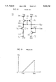
- FIG. 1 is a block diagram showing the structure of a bias generation circuit according to a first embodiment of the invention
- FIG. 2 is a graph showing the relation between input voltage V I and bias current I B in the bias generation circuit shown in FIG. 1;
- FIG. 3 is a block diagram showing the structure of a bias generation circuit according to a second embodiment of the invention.
- FIG. 4 is a block diagram showing the structure of a bias generation circuit according to a third embodiment of the invention.
- FIG. 5 is a block diagram showing the structure of a bias generation circuit according to a fourth embodiment of the invention.
- FIG. 6 is a diagram showing the structure of a bias generation circuit according to a fifth embodiment of the invention.
- FIG. 7 is a block diagram showing the structure of a general voltage controlled oscillator including a bias generation circuit
- FIG. 8 is a diagram showing the structure of the bias generation circuit in the voltage controlled oscillator shown in FIG. 7;
- FIG. 9 is a graph showing the relation between input voltage V I and bias current I B in the bias generation circuit shown in FIG. 8.
- FIG. 1 is a block diagram showing the structure of a bias generation circuit according to a first embodiment of the invention
- FIG. 2 is a graph showing the relation between input voltage V I and each current in the bias generation circuit.
- the bias generation circuit has input transistors arranged in a complementary manner, and one of the transistors is provided with current subtraction/inversion circuit 5.
- the bias generation circuit includes a P channel MOS transistor 2 (first input transistor), an N channel MOS transistor 3 (second input transistor), resistors 1 and 4, and subtraction/inversion circuit 5.
- Resistor 1 and P channel MOS transistor 2 are connected in series between a power supply node 70 and the input node 5a of subtraction/inversion circuit 5.
- N channel MOS transistor 3 and resistor 4 are connected in series between the output node 5b of subtraction/inversion circuit 5 and a ground node 71.
- Input voltage V I is input to the gates of P channel MOS transistor 2 and N channel MOS transistor 3.
- the bias generation circuit is also provided with an output circuit including P channel MOS transistors 7 and 8, and an N channel MOS transistor 9.
- P channel MOS transistor 7 is connected between power supply node 70 and a first output node N1 (the output node 5b of subtraction/inversion circuit 5), and P channel MOS transistor 8, a second output node N2, and N channel MOS transistor 9 are connected in series between power supply node 70 and ground node 71.
- the gates of P channel MOS transistors 7 and 8 are connected together to first output node N2, and the gate of N channel MOS transistor 9 is connected to second output node N2.
- Bias voltages V BB and V BN are output from first and second output nodes N1 and N2, respectively.
- current I P and current I N have inclinations opposite to each other as illustrated in FIG. 2. More specifically, current I P linearly decreases in the region in which input voltage V I is from 0 to V DD -V TP and is nullified in the range from V DD -V TP to V DD . Meanwhile, current I N is 0 in the region in which input voltage V I is from 0 to V TN and linearly increases in the region from V TN to V DD .
- P channel MOS transistors 7 and 8 constitute a current mirror circuit 6, and if P channel MOS transistors 55 and 56 are the same in size, current through P channel MOS transistor 8 is also I B . Therefore, a transistor constituting a current mirror connection with P channel MOS transistor 7 or N channel MOS transistor 9, in other words a transistor using bias voltage V BP or V BN as gate voltage forms a current source r times as large as bias current I B , where the ratio of the sizes of the transistors is r.
- resistors 1 and 4 which are provided for making the V B -I D characteristic of transistors 2 and 3 more linear may be omitted.
- FIG. 3 is a diagram showing the structure of a bias generation circuit according to a second embodiment of the invention.
- the bias generation circuit is a variation of the bias generation circuit shown in FIG. 1 with subtraction/inversion circuit 5 formed of transistors, wherein subtraction is followed by inversion.
- subtraction/inversion circuit 5 in the bias generation circuit includes a constant current source 11, and first and second current mirror circuits 12 and 15.
- First current mirror circuit 12 includes P channel MOS transistors 13 and 14, and second current mirror circuit 15 includes N channel MOS transistors 16 and 17.
- P channel MOS transistor 13 a node N11 and constant current source 11 are connected in series between power supply node 70 and ground node 71, and node N11 is connected to the drain of P channel MOS transistor 2.
- P channel MOS transistor 14, a node N12, and N channel MOS transistor 16 are connected in series between power supply node 70 and ground node 71.
- N channel MOS transistor 17 is connected between first output node N1 and ground node 71.
- the gates of P channel MOS transistors 13 and 14 are connected to node N11, and the gates of N channel MOS transistors 16 and 17 are connected to node N12.
- the other structure is substantially identical to the bias generation circuit shown in FIG. 1, and therefore a description thereof is not provided.
- FIG. 4 is a diagram showing the structure of a bias generation circuit according to a third embodiment of the invention.
- the bias generation circuit is a variation of the bias generation circuit shown in FIG. 1 with subtraction/inversion circuit 5 formed of transistors, wherein inversion is followed by subtraction.
- subtraction/inversion circuit 5 in the bias generation circuit includes a constant current source 21, first and second current mirror circuits 23 and 26.
- First current mirror circuit 22 includes N channel MOS transistors 23 and 24, and second current mirror circuit 25 includes N channel MOS transistors 26 and 27.
- N channel MOS transistors 23 and 24 are connected between nodes N21 and N22 and ground node 71, respectively, and the gates of N channel MOS transistors 23 and 24 are connected together to a node N21.
- Node N21 is connected to the drain of P channel MOS transistor 2
- node N22 is connected to power supply node 70 through constant current source 21.
- N channel MOS transistors 26 and 27 are connected between nodes N22 and N1 and ground node 71, respectively, and the gates of N channel MOS transistors 26 and 27 are connected together to node N22.
- the other structure is substantially identical to the bias generation circuit shown in FIG. 1, and therefore a description thereof is not provided.
- N channel MOS transistors 23 and 24 form a current mirror connection, and current through transistor 24 is also I P assuming that the ratio of transistor sizes is 1.
- I CONST supplied from constant current source 21 ⁇ I is generated in N channel MOS transistor 26.
- FIG. 5 is a block diagram showing a bias generation circuit according to a fourth embodiment of the invention.
- the bias generation circuit has input transistors arranged in a complementary manner, and one of the transistors is provided with a current subtraction circuit 31 and the other with a current inversion circuit 32.
- the bias generation circuit includes a P channel MOS transistor 2, an N channel MOS transistor 3, resistors 1 and 4, current subtraction circuit 32a and current inversion circuit 32.
- Resistor 1 and P channel MOS transistors 2 are connected in series between a power supply node 70 and the input node 31a of current subtraction circuit 31.
- N channel MOS transistor 3 and resistor 4 are connected in series between the input node 32a of current inversion circuit 32 and a ground node 71.
- the output node 31b of current subtraction circuit 31 and the output node 32b of current inversion circuit 32 are connected together to first output node N31.
- the bias generation circuit further includes an output circuit formed of N channel MOS transistors 34 and 35, and a P channel MOS transistor 36.
- N channel MOS transistors 34 and 35 are connected between first and second output nodes N31 and N32 and ground node 71, respectively, and the gates of N channel MOS transistors 34 and 35 are connected together to first output node N31. More specifically, N channel MOS transistors 34 and 35 constitute a current mirror circuit 33.
- P channel MOS transistor 36 is connected between power supply node 70 and second output node N32, with its gate being connected to second output node N32.
- Input voltage V I is provided to the gates of P channel MOS transistor 2 and N channel MOS transistor 3, and bias voltages V BN and V BP are output from first and second output nodes N31 and N32, respectively.
- a transistor establishing a current mirror connection with N channel MOS transistor 34 or P channel MOS transistor 36 in other words a transistor using bias voltage V BN or V BP as gate voltage forms a current source r times as large as bias current I B , assuming that the ratio of transistors sizes is r.
- one of the complementary input transistors is provided with current subtraction circuit 31, the other with current inversion circuit 32, so that the functions of current subtraction and current inversion are separated, and therefore delay until bias current I B is produced by addition can be reduced.
- FIG. 6 is a diagram showing the structure of a bias generation circuit according to a fifth embodiment of the invention.
- the bias generation circuit is a variation of the bias generation circuit shown in FIG. 5 with subtraction circuit 31 and inversion circuit 32 being formed of transistors.
- subtraction circuit 31 includes a current mirror circuit 42 and a constant current source 41
- first current mirror circuit 42 includes P channel MOS transistors 43 and 44.
- P channel MOS transistor 43 and 44 are connected between power supply node 70 and nodes N41 and N31, respectively, and the gates of P channel MOS transistors 43 and 44 are connected together to node N41.
- Constant current source 41 is connected between node N41 and ground node 71, and node N41 is connected to the drain of P channel MOS transistor 2.
- Inversion circuit 32 includes a second current mirror circuit 45, which includes P channel MOS transistors 46 and 47.
- P channel MOS transistors 46 and 47 are connected between power supply node 70 and nodes N42 and N31, respectively, and the gates of P channel MOS transistors 46 and 47 are connected together to node N42.
- Node N42 is connected to the drain of N channel MOS transistor 3.
- P channel MOS transistor 43 In response to constant current I CONST supplied from current source 41, ⁇ I is generated in P channel MOS transistor 43.
- P channel MOS transistors 43 and 44 constitute a current mirror connection, and assuming that the ratio of transistor sizes is 1, current through transistor 44 is also ⁇ I.
- P channel MOS transistors 46 and 47 also establish a current mirror connection, and assuming that the ratio of transistor sizes is 1, current through transistor 47 is I N . If the ratios of the transistor sizes are r 1 and r 2 , respectively, currents through transistors 44 and 47 are r 1 ⁇ I and r 2 ⁇ I N , respectively.
Abstract
Description
Claims (8)
Applications Claiming Priority (2)
| Application Number | Priority Date | Filing Date | Title |
|---|---|---|---|
| JP6-122521 | 1994-06-03 | ||
| JP12252194A JP3436971B2 (en) | 1994-06-03 | 1994-06-03 | Voltage controlled current source and bias generation circuit using the same |
Publications (1)
| Publication Number | Publication Date |
|---|---|
| US5543745A true US5543745A (en) | 1996-08-06 |
Family
ID=14837917
Family Applications (1)
| Application Number | Title | Priority Date | Filing Date |
|---|---|---|---|
| US08/430,675 Expired - Lifetime US5543745A (en) | 1994-06-03 | 1995-04-28 | Voltage controlled current source and bias generation circuit using such current source |
Country Status (2)
| Country | Link |
|---|---|
| US (1) | US5543745A (en) |
| JP (1) | JP3436971B2 (en) |
Cited By (15)
| Publication number | Priority date | Publication date | Assignee | Title |
|---|---|---|---|---|
| US5656954A (en) * | 1994-11-17 | 1997-08-12 | Mitsubishi Denki Kabushiki Kaisha | Current type inverter circuit, current type logic circuit, current type latch circuit, semiconductor integrated circuit, current type ring oscillator, voltage-controlled oscillator and PLL circuit |
| US5900776A (en) * | 1996-07-10 | 1999-05-04 | Motorola, Inc. | Current sense circuit |
| US5939929A (en) * | 1995-09-06 | 1999-08-17 | Advanced Micro Devices, Inc. | Low jitter low power single ended driver |
| WO2000046649A1 (en) * | 1999-02-04 | 2000-08-10 | Microchip Technology Incorporated | A current compensating bias generator and method therefor |
| US6404295B1 (en) * | 1999-09-08 | 2002-06-11 | Nec Corporation | Voltage controlled oscillator with linear input voltage characteristics |
| US20030168968A1 (en) * | 2002-03-07 | 2003-09-11 | Sanyo Electric Co., Ltd. | Layered structure of wire, a manufacturing method therefor, and an optical apparatus |
| US20030174152A1 (en) * | 2002-02-04 | 2003-09-18 | Yukihiro Noguchi | Display apparatus with function which makes gradiation control easier |
| US20030209976A1 (en) * | 2002-03-05 | 2003-11-13 | Hisashi Abe | Electroluminescent panel and a manufacturing method therefor |
| US6784702B1 (en) * | 2003-05-05 | 2004-08-31 | Winbond Electronics Corporation | Driver circuit with dynamically adjusting output current and input current-limiting function |
| US20040183427A1 (en) * | 2002-03-05 | 2004-09-23 | Sanyo Electric Co., Ltd. | Layered structure of wire (s) formed in contact hole, a manufacturing method therefor, and a display apparatus having the same |
| US7015746B1 (en) * | 2004-05-06 | 2006-03-21 | National Semiconductor Corporation | Bootstrapped bias mixer with soft start POR |
| US7030662B1 (en) * | 2003-03-25 | 2006-04-18 | Cypress Semiconductor Corporation | Rail-to-rail input linear voltage to current converter |
| US20060181324A1 (en) * | 2005-02-11 | 2006-08-17 | International Business Machines Corporation | Programmable delay element |
| US20080018320A1 (en) * | 2004-04-30 | 2008-01-24 | Jakob Jongsma | Current Balance Arrangment |
| US20130148432A1 (en) * | 2011-12-09 | 2013-06-13 | Atmel Corporation | Sense amplifier with offset current injection |
Citations (9)
| Publication number | Priority date | Publication date | Assignee | Title |
|---|---|---|---|---|
| US4342926A (en) * | 1980-11-17 | 1982-08-03 | Motorola, Inc. | Bias current reference circuit |
| DE3342735A1 (en) * | 1982-11-26 | 1984-05-30 | Tokyo Shibaura Denki K.K., Kawasaki, Kanagawa | IMPEDANCE CONVERTER CIRCUIT |
| US4558242A (en) * | 1983-02-11 | 1985-12-10 | Analog Devices, Incorporated | Extended reference range, voltage-mode CMOS D/A converter |
| US4717845A (en) * | 1987-01-02 | 1988-01-05 | Sgs Semiconductor Corporation | TTL compatible CMOS input circuit |
| US4922141A (en) * | 1986-10-07 | 1990-05-01 | Western Digital Corporation | Phase-locked loop delay line |
| WO1990014712A1 (en) * | 1989-05-24 | 1990-11-29 | Motorola, Inc. | Low current switched capacitor circuit |
| US5012133A (en) * | 1989-02-17 | 1991-04-30 | U.S. Philips Corporation | Circuit arrangement for processing sampled analog electrical signals |
| US5302920A (en) * | 1992-10-13 | 1994-04-12 | Ncr Corporation | Controllable multi-phase ring oscillators with variable current sources and capacitances |
| US5432389A (en) * | 1993-01-04 | 1995-07-11 | Motorola, Inc. | Gain stage circuit with automatic level control |
-
1994
- 1994-06-03 JP JP12252194A patent/JP3436971B2/en not_active Expired - Lifetime
-
1995
- 1995-04-28 US US08/430,675 patent/US5543745A/en not_active Expired - Lifetime
Patent Citations (9)
| Publication number | Priority date | Publication date | Assignee | Title |
|---|---|---|---|---|
| US4342926A (en) * | 1980-11-17 | 1982-08-03 | Motorola, Inc. | Bias current reference circuit |
| DE3342735A1 (en) * | 1982-11-26 | 1984-05-30 | Tokyo Shibaura Denki K.K., Kawasaki, Kanagawa | IMPEDANCE CONVERTER CIRCUIT |
| US4558242A (en) * | 1983-02-11 | 1985-12-10 | Analog Devices, Incorporated | Extended reference range, voltage-mode CMOS D/A converter |
| US4922141A (en) * | 1986-10-07 | 1990-05-01 | Western Digital Corporation | Phase-locked loop delay line |
| US4717845A (en) * | 1987-01-02 | 1988-01-05 | Sgs Semiconductor Corporation | TTL compatible CMOS input circuit |
| US5012133A (en) * | 1989-02-17 | 1991-04-30 | U.S. Philips Corporation | Circuit arrangement for processing sampled analog electrical signals |
| WO1990014712A1 (en) * | 1989-05-24 | 1990-11-29 | Motorola, Inc. | Low current switched capacitor circuit |
| US5302920A (en) * | 1992-10-13 | 1994-04-12 | Ncr Corporation | Controllable multi-phase ring oscillators with variable current sources and capacitances |
| US5432389A (en) * | 1993-01-04 | 1995-07-11 | Motorola, Inc. | Gain stage circuit with automatic level control |
Cited By (20)
| Publication number | Priority date | Publication date | Assignee | Title |
|---|---|---|---|---|
| US5656954A (en) * | 1994-11-17 | 1997-08-12 | Mitsubishi Denki Kabushiki Kaisha | Current type inverter circuit, current type logic circuit, current type latch circuit, semiconductor integrated circuit, current type ring oscillator, voltage-controlled oscillator and PLL circuit |
| US5939929A (en) * | 1995-09-06 | 1999-08-17 | Advanced Micro Devices, Inc. | Low jitter low power single ended driver |
| US5900776A (en) * | 1996-07-10 | 1999-05-04 | Motorola, Inc. | Current sense circuit |
| WO2000046649A1 (en) * | 1999-02-04 | 2000-08-10 | Microchip Technology Incorporated | A current compensating bias generator and method therefor |
| US6404295B1 (en) * | 1999-09-08 | 2002-06-11 | Nec Corporation | Voltage controlled oscillator with linear input voltage characteristics |
| US20030174152A1 (en) * | 2002-02-04 | 2003-09-18 | Yukihiro Noguchi | Display apparatus with function which makes gradiation control easier |
| US20030209976A1 (en) * | 2002-03-05 | 2003-11-13 | Hisashi Abe | Electroluminescent panel and a manufacturing method therefor |
| US20040183427A1 (en) * | 2002-03-05 | 2004-09-23 | Sanyo Electric Co., Ltd. | Layered structure of wire (s) formed in contact hole, a manufacturing method therefor, and a display apparatus having the same |
| US7150669B2 (en) | 2002-03-05 | 2006-12-19 | Sanyo Electric Co., Ltd. | Electroluminescent panel and a manufacturing method therefor |
| US20030168968A1 (en) * | 2002-03-07 | 2003-09-11 | Sanyo Electric Co., Ltd. | Layered structure of wire, a manufacturing method therefor, and an optical apparatus |
| US7078733B2 (en) | 2002-03-07 | 2006-07-18 | Sanyo Electric Co., Ltd. | Aluminum alloyed layered structure for an optical device |
| US7030662B1 (en) * | 2003-03-25 | 2006-04-18 | Cypress Semiconductor Corporation | Rail-to-rail input linear voltage to current converter |
| US6784702B1 (en) * | 2003-05-05 | 2004-08-31 | Winbond Electronics Corporation | Driver circuit with dynamically adjusting output current and input current-limiting function |
| US20080018320A1 (en) * | 2004-04-30 | 2008-01-24 | Jakob Jongsma | Current Balance Arrangment |
| US7872463B2 (en) * | 2004-04-30 | 2011-01-18 | Austriamicrosystems Ag | Current balance arrangement |
| US7015746B1 (en) * | 2004-05-06 | 2006-03-21 | National Semiconductor Corporation | Bootstrapped bias mixer with soft start POR |
| US7279949B2 (en) * | 2005-02-11 | 2007-10-09 | International Business Machines Corporation | Programmable delay element |
| US20060181324A1 (en) * | 2005-02-11 | 2006-08-17 | International Business Machines Corporation | Programmable delay element |
| US20130148432A1 (en) * | 2011-12-09 | 2013-06-13 | Atmel Corporation | Sense amplifier with offset current injection |
| US8830759B2 (en) * | 2011-12-09 | 2014-09-09 | Atmel Corporation | Sense amplifier with offset current injection |
Also Published As
| Publication number | Publication date |
|---|---|
| JPH07336172A (en) | 1995-12-22 |
| JP3436971B2 (en) | 2003-08-18 |
Similar Documents
| Publication | Publication Date | Title |
|---|---|---|
| US5543745A (en) | Voltage controlled current source and bias generation circuit using such current source | |
| EP0318396B1 (en) | Operational amplifier circuit having stable operating point | |
| JP2525346B2 (en) | Differential amplifier circuit having constant current source circuit | |
| US4471292A (en) | MOS Current mirror with high impedance output | |
| US5612614A (en) | Current mirror and self-starting reference current generator | |
| KR20000077108A (en) | Voltage-controlled oscillator | |
| US6181191B1 (en) | Dual current source circuit with temperature coefficients of equal and opposite magnitude | |
| JPH05145384A (en) | Cmos receiver input interface circuit | |
| US6731169B2 (en) | Differential amplifier circuit | |
| US4983929A (en) | Cascode current mirror | |
| US5929679A (en) | Voltage monitoring circuit capable of reducing power dissipation | |
| KR0126911B1 (en) | Circuit and method for voltage reference generating | |
| JP3234732B2 (en) | Level conversion circuit | |
| US4947140A (en) | Voltage controlled oscillator using differential CMOS circuit | |
| KR950010335A (en) | Cascode circuit with high output impedance, capable of operating at low operating voltages | |
| KR920010237B1 (en) | Amplifier | |
| US4812681A (en) | NMOS analog voltage comparator | |
| KR0132646B1 (en) | Voltage to current conversion circuit utilizing mos transistor | |
| KR100363139B1 (en) | Buffer Circuit and Bias Circuit | |
| WO1989006837A1 (en) | Voltage sources | |
| GB2209254A (en) | Current minor amplifier with reduced supply voltage sensitivity | |
| JPS63276316A (en) | Oscillation circuit | |
| JP3194430B2 (en) | Current switch circuit | |
| KR20060065444A (en) | Variable gain amplifier | |
| KR100344635B1 (en) | Three dimension functional voltage generating circuit |
Legal Events
| Date | Code | Title | Description |
|---|---|---|---|
| AS | Assignment |
Owner name: MITSUBISHI DENKI KABUSHIKI KAISHA, JAPAN Free format text: ASSIGNMENT OF ASSIGNORS INTEREST;ASSIGNOR:NOTANI, HIROMI;REEL/FRAME:007592/0827 Effective date: 19950308 |
|
| STCF | Information on status: patent grant |
Free format text: PATENTED CASE |
|
| FEPP | Fee payment procedure |
Free format text: PAYOR NUMBER ASSIGNED (ORIGINAL EVENT CODE: ASPN); ENTITY STATUS OF PATENT OWNER: LARGE ENTITY |
|
| FPAY | Fee payment |
Year of fee payment: 4 |
|
| FPAY | Fee payment |
Year of fee payment: 8 |
|
| FPAY | Fee payment |
Year of fee payment: 12 |
|
| AS | Assignment |
Owner name: RENESAS ELECTRONICS CORPORATION, JAPAN Free format text: ASSIGNMENT OF ASSIGNORS INTEREST;ASSIGNOR:MITSUBISHI DENKI KABUSHIKI KAISHA;REEL/FRAME:025980/0219 Effective date: 20110307 |