US5541948A - Transition-metal doped sulfide, selenide, and telluride laser crystal and lasers - Google Patents
Transition-metal doped sulfide, selenide, and telluride laser crystal and lasers Download PDFInfo
- Publication number
- US5541948A US5541948A US08/346,457 US34645794A US5541948A US 5541948 A US5541948 A US 5541948A US 34645794 A US34645794 A US 34645794A US 5541948 A US5541948 A US 5541948A
- Authority
- US
- United States
- Prior art keywords
- transition metal
- group
- laser
- metal ion
- host material
- Prior art date
- Legal status (The legal status is an assumption and is not a legal conclusion. Google has not performed a legal analysis and makes no representation as to the accuracy of the status listed.)
- Expired - Lifetime
Links
Images


Classifications
-
- H—ELECTRICITY
- H01—ELECTRIC ELEMENTS
- H01S—DEVICES USING THE PROCESS OF LIGHT AMPLIFICATION BY STIMULATED EMISSION OF RADIATION [LASER] TO AMPLIFY OR GENERATE LIGHT; DEVICES USING STIMULATED EMISSION OF ELECTROMAGNETIC RADIATION IN WAVE RANGES OTHER THAN OPTICAL
- H01S3/00—Lasers, i.e. devices using stimulated emission of electromagnetic radiation in the infrared, visible or ultraviolet wave range
- H01S3/14—Lasers, i.e. devices using stimulated emission of electromagnetic radiation in the infrared, visible or ultraviolet wave range characterised by the material used as the active medium
- H01S3/16—Solid materials
-
- H—ELECTRICITY
- H01—ELECTRIC ELEMENTS
- H01S—DEVICES USING THE PROCESS OF LIGHT AMPLIFICATION BY STIMULATED EMISSION OF RADIATION [LASER] TO AMPLIFY OR GENERATE LIGHT; DEVICES USING STIMULATED EMISSION OF ELECTROMAGNETIC RADIATION IN WAVE RANGES OTHER THAN OPTICAL
- H01S3/00—Lasers, i.e. devices using stimulated emission of electromagnetic radiation in the infrared, visible or ultraviolet wave range
- H01S3/10—Controlling the intensity, frequency, phase, polarisation or direction of the emitted radiation, e.g. switching, gating, modulating or demodulating
- H01S3/106—Controlling the intensity, frequency, phase, polarisation or direction of the emitted radiation, e.g. switching, gating, modulating or demodulating by controlling devices placed within the cavity
- H01S3/108—Controlling the intensity, frequency, phase, polarisation or direction of the emitted radiation, e.g. switching, gating, modulating or demodulating by controlling devices placed within the cavity using non-linear optical devices, e.g. exhibiting Brillouin or Raman scattering
- H01S3/109—Frequency multiplication, e.g. harmonic generation
- H01S3/1095—Frequency multiplication, e.g. harmonic generation self doubling, e.g. lasing and frequency doubling by the same active medium
-
- H—ELECTRICITY
- H01—ELECTRIC ELEMENTS
- H01S—DEVICES USING THE PROCESS OF LIGHT AMPLIFICATION BY STIMULATED EMISSION OF RADIATION [LASER] TO AMPLIFY OR GENERATE LIGHT; DEVICES USING STIMULATED EMISSION OF ELECTROMAGNETIC RADIATION IN WAVE RANGES OTHER THAN OPTICAL
- H01S3/00—Lasers, i.e. devices using stimulated emission of electromagnetic radiation in the infrared, visible or ultraviolet wave range
- H01S3/10—Controlling the intensity, frequency, phase, polarisation or direction of the emitted radiation, e.g. switching, gating, modulating or demodulating
- H01S3/11—Mode locking; Q-switching; Other giant-pulse techniques, e.g. cavity dumping
- H01S3/1106—Mode locking
- H01S3/1112—Passive mode locking
-
- H—ELECTRICITY
- H01—ELECTRIC ELEMENTS
- H01S—DEVICES USING THE PROCESS OF LIGHT AMPLIFICATION BY STIMULATED EMISSION OF RADIATION [LASER] TO AMPLIFY OR GENERATE LIGHT; DEVICES USING STIMULATED EMISSION OF ELECTROMAGNETIC RADIATION IN WAVE RANGES OTHER THAN OPTICAL
- H01S3/00—Lasers, i.e. devices using stimulated emission of electromagnetic radiation in the infrared, visible or ultraviolet wave range
- H01S3/14—Lasers, i.e. devices using stimulated emission of electromagnetic radiation in the infrared, visible or ultraviolet wave range characterised by the material used as the active medium
- H01S3/16—Solid materials
- H01S3/1685—Ceramics
-
- H—ELECTRICITY
- H01—ELECTRIC ELEMENTS
- H01S—DEVICES USING THE PROCESS OF LIGHT AMPLIFICATION BY STIMULATED EMISSION OF RADIATION [LASER] TO AMPLIFY OR GENERATE LIGHT; DEVICES USING STIMULATED EMISSION OF ELECTROMAGNETIC RADIATION IN WAVE RANGES OTHER THAN OPTICAL
- H01S3/00—Lasers, i.e. devices using stimulated emission of electromagnetic radiation in the infrared, visible or ultraviolet wave range
- H01S3/14—Lasers, i.e. devices using stimulated emission of electromagnetic radiation in the infrared, visible or ultraviolet wave range characterised by the material used as the active medium
- H01S3/16—Solid materials
- H01S3/1601—Solid materials characterised by an active (lasing) ion
- H01S3/162—Solid materials characterised by an active (lasing) ion transition metal
- H01S3/1621—Solid materials characterised by an active (lasing) ion transition metal cobalt
-
- H—ELECTRICITY
- H01—ELECTRIC ELEMENTS
- H01S—DEVICES USING THE PROCESS OF LIGHT AMPLIFICATION BY STIMULATED EMISSION OF RADIATION [LASER] TO AMPLIFY OR GENERATE LIGHT; DEVICES USING STIMULATED EMISSION OF ELECTROMAGNETIC RADIATION IN WAVE RANGES OTHER THAN OPTICAL
- H01S3/00—Lasers, i.e. devices using stimulated emission of electromagnetic radiation in the infrared, visible or ultraviolet wave range
- H01S3/14—Lasers, i.e. devices using stimulated emission of electromagnetic radiation in the infrared, visible or ultraviolet wave range characterised by the material used as the active medium
- H01S3/16—Solid materials
- H01S3/1601—Solid materials characterised by an active (lasing) ion
- H01S3/162—Solid materials characterised by an active (lasing) ion transition metal
- H01S3/1623—Solid materials characterised by an active (lasing) ion transition metal chromium, e.g. Alexandrite
-
- H—ELECTRICITY
- H01—ELECTRIC ELEMENTS
- H01S—DEVICES USING THE PROCESS OF LIGHT AMPLIFICATION BY STIMULATED EMISSION OF RADIATION [LASER] TO AMPLIFY OR GENERATE LIGHT; DEVICES USING STIMULATED EMISSION OF ELECTROMAGNETIC RADIATION IN WAVE RANGES OTHER THAN OPTICAL
- H01S3/00—Lasers, i.e. devices using stimulated emission of electromagnetic radiation in the infrared, visible or ultraviolet wave range
- H01S3/14—Lasers, i.e. devices using stimulated emission of electromagnetic radiation in the infrared, visible or ultraviolet wave range characterised by the material used as the active medium
- H01S3/16—Solid materials
- H01S3/1628—Solid materials characterised by a semiconducting matrix
Definitions
- the invention relates generally to solid state lasers, and more particularly to solid state laser materials.
- Fluoride and oxide crystals doped with transition metal ions have long been known to serve usefully as laser materials.
- the first laser was a flashlamp-pumped ruby, which is Cr 3+ -doped Al 2 O 3 [Maiman, "Stimulated optical radiation in ruby," Nature 187, 493 (1960)].
- the Cr 3+ dopants color the Al 2 O 3 crystals (sapphire) pink or red, and are responsible for the laser activity of the medium. While the ruby laser once aroused much interest and exploration, it ultimately proved to be of limited utility.
- One limitation of the material is its narrow gain spectrum (centered at 692 nm); a broader gain spectrum would prove to be more useful.
- the first broadly tunable gain media based on the transition metal ions Ni 2+ , Co 2+ and V 2+ , were discovered by L. Johnson and coworkers [L. F. Johnson et al., "Phonon terminated optical masers," Phys. Rev. 149, 179 (1966); also Auzel et al., U.S. Pat. No. 4,627,064]. Again, these lasers did not turn out to be of substantial practical interest since several fundamental issues limit their utility. For example, both Ni 2+ and V 2+ -based lasers tend to operate with low efficiency [S. A. Payne et al., "Excited state absorption spectra of V 2+ in KMgF 3 and MgF 2 ,” Phys.
- ESA Excited state absorption
- Nonradiative decay is also detrimental to the operation of the laser since the energy stored in the excited states that are produced lead to heat generation, rather than to light (and therefore to gain).
- Co 2+ -based lasers such as Co:MgF 2 experience low ESA loss although the nonradiative decay is substantial [D. M. Rines et al., "High energy operation of a Co:MgF 2 laser,” Opt. Lett. 19, 628 (1994)].
- Rines et al. has shown that the Co:MgF 2 laser can operate efficiently if it is pumped with a ⁇ 50 ⁇ sec pulse from a 1.3 ⁇ m Nd:YAG laser, although the overall efficiency of this laser-pumped laser system remains low.
- transition metal ion is coordinated by six fluorines or six oxygens in an octahedral site.
- known laser materials based on transition metal ions primarily involve octahedral coordination of the laser ions, there are a few examples where tetrahedral, or four-fold coordinated, sites are employed.
- the main transition metal ions of this nature include Cr 4+ , and to a lesser extent, Mn 5+ (Alfano, U.S. Pat. No. 4,932,031 and Alfano, U.S. Pat. No. 4,987,575).
- the present invention is based on transition metal ions that are incorporated onto tetrahedral sites.
- III-V notation refers to the number of valence electrons in the neutral state of the cation (e.g., In with three electrons) and for the anion (e.g., P with five electrons).
- II-VI compounds such as ZnS.
- Transition metal ion dopants in II-VI compounds emitting in the visible spectral range have previously been recognized to serve usefully in fluorescence display materials (e.g., Goede et al., German Patent No. DD 251,153; Mullermach et al., German Patent No. DD 255,429; and Japanese Patent Nos. JP 56088487 and JP 85008073). In these cases, the transition metal doped II-VI compounds are considered for electroluminescence behavior rather than as laser materials.
- the observed emission lifetime is a useful quantity from which to judge the potential for laser action, since in some circumstances it may be employed to calculate the emission cross section.
- an abrupt decrease in the emission lifetime with rising temperature may be interpreted as the onset of nonradiative decay (i.e., the decrease in luminescence yield).
- crystals are selected to offer tetrahedral sites (fourfold coordinated) into which the dopants are incorporated.
- One particular embodiment of this invention is Cr 2+ -doped crystals, such as ZnS, ZnSe, ZnTe, CdS, CdSe, CdTe, CaGa 2 S 4 , CaGa 2 Se 4 , CdGa 2 S 4 and CdGa 2 Se 4 .
- Other laser ions include Fe 2+ and Co 2+ .
- the laser materials may be arranged in laser systems, as a thin-film waveguide structure, or as the active medium in a laser diode. Furthermore, said gain medium may be pumped by other laser diodes.
- Another object of the invention is to provide Cr 2+ -doped host crystals possessing substitutional tetrahedral sites, including oxides, fluorides, chlorides, bromides and iodides, in addition to the aforementioned sulfides, selenides and tellurides.
- Preferred embodiments of said saturable absorber media include Cr 2+ or Fe 2+ in ZnS, ZnSe, ZnTe, CdS, CdSe and CdTe.
- FIGS. 1a, b, c show the room temperature absorption spectra of Cr 2+ dopants in ZnS, ZnSe and ZnTe.
- FIG. 2 is a Tanabe-Sugano diagram that describes the energy levels of a d 4 transition metal ion in tetrahedral symmetry.
- FIGS. 3a, b, c depict the emission spectra of Cr 2+ dopants in ZnS, ZnSe and ZnTe at room temperature.
- FIGS. 4a, b, c are plots of the emission lifetimes of the Cr 2+ dopant in ZnS, ZnSe and ZnTe as a function of temperature.
- FIG. 5 is a plot of the 2.3 ⁇ m output energy generated from a Cr 2+ :ZnSe laser as a function of the 1.8 ⁇ m pump energy.
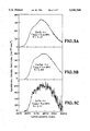
- FIGS. 6a, b, c display the room temperature emission spectra obtained from Co 2+ -doped ZnS, ZnSe and ZnTe.
- FIGS. 7a, b, c are plots of the emission lifetimes of the Co 2+ dopant in ZnS, ZnSe and ZnTe as a function of temperature.
- FIG. 8 shows a generic laser apparatus into which the new class of laser materials can be incorporated.
- the invention is a solid state laser material and laser comprised of transition metal doped II-VI compounds.
- the invention includes transition metal-doped sulfide, selenide, and telluride materials (also referred to as chalcogenides).
- the invention includes the Cr 2+ , Co 2+ , Fe 2+ and other transition metal ions in sulfide, selenide, telluride and other host crystals offering tetrahedral (four-fold coordinated) substitutional sites, into which the transition metal ions can be incorporated.
- Embodiments include Cr 2+ , Co 2+ or Fe 2+ in the zinc chalcogenides, cadmium chalcogenides, CdGa 2 S 4 , CaGa 2 S 4 , and other chalcogenide crystals.
- One particular embodiment of the invention is Cr 2+ -doped ZnS, ZnSe or ZnTe. In these cases the Cr 2+ ions substitute for the Zn 2+ host ion and thereby occupy a tetrahedral four-fold coordinated site.
- the absorption spectra of the crystals are shown in FIGS. 1a, b, c.
- the main absorption band occurring in the 1.5-2.0 ⁇ m region arises from the 5 E ⁇ 5T 2 transition.
- the energy levels of Cr 2+ can be understood on the basis of the well-known Tanabe-Sugano diagram, as is reproduced in FIG. 2.
- the ordinate of this plot is the normalized energy levels of the Cr 2+ electronic states while the abscissa is a measure of the tetrahedral field strength experienced by the Cr 2+ ion.
- the far left of the abscissa represents the free-ion levels while the crystal field strength increases in proceeding to the right-hand side; (the arrow denotes the approximate field relevant to the Cr 2+ -doped II-VI compounds).
- the high efficiency can be attributed, in part, to the tetrahedral symmetry of the lattice site into which the Cr 2+ ion is incorporated.
- the tetrahedral four-fold coordinated site does not possess a center of inversion and therefore induces a strong dipole moment into the emission transition.
- the resulting greatly enhanced emission rates can accordingly compete more effectively with the temperature-dependent nonradiative decay rate.
- the tetrahedral character of the site in the II-VI compound is, in fact, one of the key features of this new class of laser materials. (Recall that virtually all existing laser hosts for transition metal ions are based on octahedral, or sixfold coordinated sites.) The tetrahedral sites also lead to a crystal field strength that is substantially weaker than that of octahedral sites, thereby shifting the emission band into the technologically important mid-infrared region (i.e., the Dq/B value of FIG. 2 is smaller for tetrahedral sites).
- the Cr 2+ :ZnSe crystal has been demonstrated to lase using a straightforward laser cavity configuration, in which the Cr:ZnSe crystal was placed symmetrically between two parallel mirrors. One mirror is highly-reflecting at the peak emission wavelength of 2.3 ⁇ m, while the other cavity mirror (i.e., the output coupler) transmits about 8% at 2.3 ⁇ m.
- a commercial Co:MgF 2 laser operating at 1.8 ⁇ m is employed as the pump source.
- the results of the Cr 2+ :ZnSe laser demonstrations are displayed in FIG. 5, where it is seen that the conversion efficiency for 2.3 ⁇ m output energy compared to the absorbed 1.8 ⁇ m pump energy is about 20%. This data definitively proves that the Cr 2+ -doped II-VI compounds represent a new class of laser materials. It furthermore broadly suggests that other transition metal ions in these II-VI crystals as well as other related materials may prove useful as lasers.
- the 3d 4 electronic structure of Cr 2+ together with the tetrahedral environment, gives rise to the energy levels depicted in FIG. 2.
- This favorable energy level structure can also be realized on the basis of second or third row transition metal ions having the 4d 4 and 5d 4 electronic configurations.
- other first row transition metal ions having the 3d 4 configuration may prove useful, such as Mn 3+ . While requiring that these transition metal ions be located in a lattice site of tetrahedral-type symmetry, there is no physical reason to limit the invention to the II-VI sulfide, selenide or telluride compounds noted above. For example, CdS, CdSe, and CdTe are well-known compounds that may prove useful.
- More complex crystals such as ZnGa 2 S 4 , CaGa 2 S 4 , ZnGa 2 Se 4 , CdGa 2 S 4 , CaGa 2 Se 4 , and CdGa 2 Se 4 may also be worthwhile.
- Oxides, fluorides, chlorides, bromides and iodides are also worthy of consideration if they have the appropriate tetrahedral sites available for substitution by transition metal ions.
- the emission spectra of the Co 2+ transition metal ion in ZnS, ZnSe and ZnTe are displayed in FIGS. 6a, b, c, from which it is deduced that these materials could potentially lase in the 3-4 ⁇ m region.
- the emission cross sections are much smaller than the values observed for Cr 2+ in FIGS. 3a, b, c.
- the low emission cross section evidenced by the Co 2+ -doped crystals can be interpreted to suggest that ESA transitions may overwhelm any prospect for laser action in the 3-4 ⁇ m region.
- the emission band may occur in a region for which ESA losses are fortuitously low.
- the emission lifetimes of the Co 2+ -doped II-VI crystals are plotted in FIGS. 7a, b, c, where it is seen that the emission lifetime decreases abruptly somewhat below room temperature.
- the strong influence of nonradiative decay at room temperature is likely to adversely impact the prospects for laser action among the Co 2+ -doped materials.
- the pump source (2) can be a laser diode, a laser diode array, or another laser arranged to longitudinally pump the gain medium (4) through the resonator mirror (6).
- the gain medium may also be fabricated as a waveguiding structure or simply as a bulk material.
- the output coupling mirror (8) is carefully aligned to form the laser resonator.
- the output beam (10) is generated by energizing the gain medium with the pump source.
- Alternative embodiments of the laser apparatus entail pumping transverse to the optic axis of the cavity and the use of flashlamps instead of laser sources.
- Additional optics (12) may be included in the cavity in order to Q-switch, modelock, wavelength tune, line-narrow or otherwise manipulate the properties of the laser beam that is generated by the apparatus.
- the gain medium can be utilized in a laser amplifier (instead of an oscillator), wherein an injected beam is enhanced in energy or power.
- Another embodiment of the invention can involve a laser diode device, where the gain medium serves as the active element and is energized by passing current through the lasing region.
- the transition metal doped II-VI compound is sandwiched between n- and p-type semiconductor materials.
- a final embodiment of this class of materials involves its use as saturable absorbers.
- This application of the materials is related to their use as gain media in that both applications require that there be low ESA loss at the pump wavelength, and that the cross sections be large (as occurs for lattice sites of tetrahedral symmetry).
- This type of scenario can be realized for the Cr 2+ and Fe 2+ -doped crystals, since the prominent absorption feature offers a large cross section, while all of the ESA transitions are expected to be weak and spin-forbidden.
- a saturable absorber when placed in a laser cavity of FIG. 8 as component 12, will cause the apparatus to generate short (psec or nsec) bursts of light, rather than a long pulse.
- One specific example of such a system could involve Fe 2+ :ZnSe as the saturable absorber optic for a Cr 2+ :ZnSe laser. In this way the Fe:ZnSe optic will initially hold off the gain in the cavity by spoiling the Q ("quality factor"), until the Fe 2+ absorption becomes saturated (i.e., bleached to transparency) such that a short intense pulse is generated by the laser apparatus.
- the ZnS, ZnSe, ZnTe, CdS, CdSe and CdTe crystals can be produced in two material forms: as a single crystal or as a fused polycrystalline material. In either case the transition metal doped crystal is judged to be useful as gain media and saturable absorbers.
Abstract
Description
Claims (20)
Priority Applications (1)
| Application Number | Priority Date | Filing Date | Title |
|---|---|---|---|
| US08/346,457 US5541948A (en) | 1994-11-28 | 1994-11-28 | Transition-metal doped sulfide, selenide, and telluride laser crystal and lasers |
Applications Claiming Priority (1)
| Application Number | Priority Date | Filing Date | Title |
|---|---|---|---|
| US08/346,457 US5541948A (en) | 1994-11-28 | 1994-11-28 | Transition-metal doped sulfide, selenide, and telluride laser crystal and lasers |
Publications (1)
| Publication Number | Publication Date |
|---|---|
| US5541948A true US5541948A (en) | 1996-07-30 |
Family
ID=23359481
Family Applications (1)
| Application Number | Title | Priority Date | Filing Date |
|---|---|---|---|
| US08/346,457 Expired - Lifetime US5541948A (en) | 1994-11-28 | 1994-11-28 | Transition-metal doped sulfide, selenide, and telluride laser crystal and lasers |
Country Status (1)
| Country | Link |
|---|---|
| US (1) | US5541948A (en) |
Cited By (47)
| Publication number | Priority date | Publication date | Assignee | Title |
|---|---|---|---|---|
| EP0855770A2 (en) * | 1997-01-24 | 1998-07-29 | HE HOLDINGS, INC. dba HUGHES ELECTRONICS | Eyesafe laser system using transition metal-doped group II-VI semiconductor as a passive saturable absorber Q-switch |
| US5802083A (en) * | 1995-12-11 | 1998-09-01 | Milton Birnbaum | Saturable absorber Q-switches for 2-μm lasers |
| US6167069A (en) * | 1998-05-01 | 2000-12-26 | The Regents Of The University Of California | Thermal lens elimination by gradient-reduced zone coupling of optical beams |
| US6207229B1 (en) * | 1997-11-13 | 2001-03-27 | Massachusetts Institute Of Technology | Highly luminescent color-selective materials and method of making thereof |
| US6251303B1 (en) | 1998-09-18 | 2001-06-26 | Massachusetts Institute Of Technology | Water-soluble fluorescent nanocrystals |
| US6273883B1 (en) | 1996-04-09 | 2001-08-14 | Cynosure, Inc. | Alexandrite laser system for treatment of dermatological specimens |
| US6306610B1 (en) | 1998-09-18 | 2001-10-23 | Massachusetts Institute Of Technology | Biological applications of quantum dots |
| WO2002021648A1 (en) * | 2000-09-06 | 2002-03-14 | West Virginia University | Transition metal-doped ii-vi heterostructure waveguide light emitter |
| WO2002078585A2 (en) * | 2001-03-30 | 2002-10-10 | Carl Zeiss Meditec Ag | Device and method for the laser treatment of organic material |
| WO2003026086A1 (en) * | 2001-09-20 | 2003-03-27 | University Of Alabama At Birmingham Research Foundation | MID-IR MICROCHIP LASER: ZnS:Cr2+ LASER WITH SATURABLE ABSORBER MATERIAL |
| US20030142944A1 (en) * | 2001-09-17 | 2003-07-31 | Sundar Vikram C. | Semiconductor nanocrystal composite |
| US6602671B1 (en) | 1998-09-18 | 2003-08-05 | Massachusetts Institute Of Technology | Semiconductor nanocrystals for inventory control |
| US6607829B1 (en) | 1997-11-13 | 2003-08-19 | Massachusetts Institute Of Technology | Tellurium-containing nanocrystalline materials |
| US6650670B1 (en) * | 2000-07-13 | 2003-11-18 | Yutaka Shimoji | Polycrystalline ceramic laser |
| US20040004982A1 (en) * | 2001-11-16 | 2004-01-08 | Eisler Hans J. | Nanocrystal structures |
| US20040110002A1 (en) * | 2002-08-13 | 2004-06-10 | Sungjee Kim | Semiconductor nanocrystal heterostructures |
| US6819692B2 (en) | 2000-03-14 | 2004-11-16 | Massachusetts Institute Of Technology | Optical amplifiers and lasers |
| US20050112849A1 (en) * | 2003-08-26 | 2005-05-26 | Stott Nathan E. | Method of preparing nanocrystals |
| US20050147974A1 (en) * | 2002-03-30 | 2005-07-07 | Muller-Shulte Detlef P. | Luminescent, spherical, non-autofluorescent silica gel particles having variable emission intensities and frequencies |
| US20050258418A1 (en) * | 2004-03-08 | 2005-11-24 | Steckel Jonathan S | Blue light emitting semiconductor nanocrystal materials |
| US20060019098A1 (en) * | 2004-07-26 | 2006-01-26 | Chan Yinthai | Microspheres including nanoparticles |
| US20060060862A1 (en) * | 2001-02-09 | 2006-03-23 | Massachusetts Institute Of Technology | Composite material including nanocrystals and methods of making |
| US20060157720A1 (en) * | 2005-01-11 | 2006-07-20 | Bawendi Moungi G | Nanocrystals including III-V semiconductors |
| US20070045597A1 (en) * | 2005-01-24 | 2007-03-01 | Research Foundation Of The City University Of New York | Cr3+-doped laser materials and lasers and methods of making and using |
| US20070064748A1 (en) * | 2001-09-20 | 2007-03-22 | Sergey Mirov | Mid-IR laser instrument for analyzing a gaseous sample and method for using the same |
| US20070152236A1 (en) * | 2005-12-29 | 2007-07-05 | Halpert Jonathan E | Semiconductor nanocrystal heterostructures |
| US20070197003A1 (en) * | 2004-09-24 | 2007-08-23 | Brian Yen | Flow method and reactor for manufacturing nanocrystals |
| US7319709B2 (en) | 2002-07-23 | 2008-01-15 | Massachusetts Institute Of Technology | Creating photon atoms |
| US20080033411A1 (en) * | 2006-07-14 | 2008-02-07 | Biolase Technology, Inc. | High efficiency electromagnetic laser energy cutting device |
| US20080090327A1 (en) * | 2001-04-04 | 2008-04-17 | Nippon Mining & Netals Co., Ltd. | Method for producing ZnTe system compound semiconductor single crystal, ZnTe system compound semiconductor single crystal, and semiconductor device |
| US20080101423A1 (en) * | 2002-09-19 | 2008-05-01 | Sergey Mirov | Saturable absorbers for q-switching of middle infrared laser cavaties |
| US20090122816A1 (en) * | 2005-09-22 | 2009-05-14 | Lockheed Martin Coherent Technologies, Inc. | Rapidly and electronically broadly tunable IR laser source |
| US20090191567A1 (en) | 1997-11-25 | 2009-07-30 | The Regents Of The University Of California | Semiconductor nanocrystal probes for biological applications and process for making and using such probes |
| US7912653B1 (en) | 2003-04-17 | 2011-03-22 | Nanosys, Inc. | Nanocrystal taggants |
| US8071466B1 (en) | 2007-12-28 | 2011-12-06 | Fairfield Crystal Technology, Llc | Zinc sulfide crystals for optical components |
| DE102011054024A1 (en) * | 2011-09-28 | 2013-03-28 | Deutsches Zentrum für Luft- und Raumfahrt e.V. | Infrared laser amplifier system for creating laser radiation field in specific wavelength range, has laser radiation field waist lying within solid bodies, where pump radiation field focusing unit has specific radio frequency |
| CN104009376A (en) * | 2014-05-06 | 2014-08-27 | 北京工业大学 | Mid-infrared super-continuum spectrum light source for Cr:II-VI-family crystal laser pumping |
| US8915948B2 (en) | 2002-06-19 | 2014-12-23 | Palomar Medical Technologies, Llc | Method and apparatus for photothermal treatment of tissue at depth |
| US9028536B2 (en) | 2006-08-02 | 2015-05-12 | Cynosure, Inc. | Picosecond laser apparatus and methods for its operation and use |
| US20160268765A1 (en) * | 2013-10-25 | 2016-09-15 | Atla Lasers As | Laser Crystal |
| WO2017139617A1 (en) * | 2016-02-12 | 2017-08-17 | Ipg Photonics Corporation | High power cw mid-ir laser |
| US9780518B2 (en) | 2012-04-18 | 2017-10-03 | Cynosure, Inc. | Picosecond laser apparatus and methods for treating target tissues with same |
| US10245107B2 (en) | 2013-03-15 | 2019-04-02 | Cynosure, Inc. | Picosecond optical radiation systems and methods of use |
| US10434324B2 (en) | 2005-04-22 | 2019-10-08 | Cynosure, Llc | Methods and systems for laser treatment using non-uniform output beam |
| CN114380599A (en) * | 2022-01-26 | 2022-04-22 | 中国工程物理研究院化工材料研究所 | Preparation method of transition metal ion doped zinc selenide laser transparent ceramic |
| US11418000B2 (en) | 2018-02-26 | 2022-08-16 | Cynosure, Llc | Q-switched cavity dumped sub-nanosecond laser |
| CN115928216A (en) * | 2022-11-28 | 2023-04-07 | 黑龙江工程学院 | Method for reducing absorption loss of iron-doped zinc selenide crystal by utilizing electron irradiation |
Citations (13)
| Publication number | Priority date | Publication date | Assignee | Title |
|---|---|---|---|---|
| US4000247A (en) * | 1974-05-27 | 1976-12-28 | Nippon Telegraph And Telephone Public Corporation | Dielectric active medium for lasers |
| US4081763A (en) * | 1973-01-04 | 1978-03-28 | Natalya Andreevna Vlasenko | Electroluminescent laser |
| US4377864A (en) * | 1981-08-10 | 1983-03-22 | Gte Laboratories Incorporated | Chromium (III) ordered perovskite lasers and media therefor |
| US4627064A (en) * | 1983-11-22 | 1986-12-02 | L'etat Francais Represente Par Le Ministre Des P.T.T. (C.N.E.T.) | Mixed oxides for tunable lasers |
| US4648094A (en) * | 1984-06-08 | 1987-03-03 | Gte Laboratories Incorporated | Chromium (3+) doped germanate garnets as active media for tunable solid state lasers |
| US4935934A (en) * | 1986-06-10 | 1990-06-19 | Centre National De La Recherche Scientifique | Mixed lanthanide-magnesium gallates and laser using monocrystals of these gallates |
| US4987575A (en) * | 1987-12-04 | 1991-01-22 | Alfano Robert R | Tetravalent chromium (Cr4+) as a laser-active ion for tunabale solid-state lasers |
| US5140604A (en) * | 1990-03-13 | 1992-08-18 | Quartz Et Silice | Mixed strontium and lanthanide oxides and a laser using monocrystals of these oxides |
| US5166948A (en) * | 1991-06-19 | 1992-11-24 | Polaroid Corporation | Optically pumped up converting light source |
| US5173911A (en) * | 1990-10-25 | 1992-12-22 | Commissariat A L'energie Atomique | Mixed silicates of yttrium and lanthanide and laser using monocrystals of these silicates |
| US5287373A (en) * | 1992-08-17 | 1994-02-15 | Alliedsignal Inc. | Gradient doped solid state laser gain media |
| US5319653A (en) * | 1991-11-20 | 1994-06-07 | France Telecom | Integrated optical component structure |
| US5422907A (en) * | 1994-05-20 | 1995-06-06 | Bhargava; Rameshwar N. | Pumped solid-state lasers comprising doped nanocrystal phosphors |
-
1994
- 1994-11-28 US US08/346,457 patent/US5541948A/en not_active Expired - Lifetime
Patent Citations (13)
| Publication number | Priority date | Publication date | Assignee | Title |
|---|---|---|---|---|
| US4081763A (en) * | 1973-01-04 | 1978-03-28 | Natalya Andreevna Vlasenko | Electroluminescent laser |
| US4000247A (en) * | 1974-05-27 | 1976-12-28 | Nippon Telegraph And Telephone Public Corporation | Dielectric active medium for lasers |
| US4377864A (en) * | 1981-08-10 | 1983-03-22 | Gte Laboratories Incorporated | Chromium (III) ordered perovskite lasers and media therefor |
| US4627064A (en) * | 1983-11-22 | 1986-12-02 | L'etat Francais Represente Par Le Ministre Des P.T.T. (C.N.E.T.) | Mixed oxides for tunable lasers |
| US4648094A (en) * | 1984-06-08 | 1987-03-03 | Gte Laboratories Incorporated | Chromium (3+) doped germanate garnets as active media for tunable solid state lasers |
| US4935934A (en) * | 1986-06-10 | 1990-06-19 | Centre National De La Recherche Scientifique | Mixed lanthanide-magnesium gallates and laser using monocrystals of these gallates |
| US4987575A (en) * | 1987-12-04 | 1991-01-22 | Alfano Robert R | Tetravalent chromium (Cr4+) as a laser-active ion for tunabale solid-state lasers |
| US5140604A (en) * | 1990-03-13 | 1992-08-18 | Quartz Et Silice | Mixed strontium and lanthanide oxides and a laser using monocrystals of these oxides |
| US5173911A (en) * | 1990-10-25 | 1992-12-22 | Commissariat A L'energie Atomique | Mixed silicates of yttrium and lanthanide and laser using monocrystals of these silicates |
| US5166948A (en) * | 1991-06-19 | 1992-11-24 | Polaroid Corporation | Optically pumped up converting light source |
| US5319653A (en) * | 1991-11-20 | 1994-06-07 | France Telecom | Integrated optical component structure |
| US5287373A (en) * | 1992-08-17 | 1994-02-15 | Alliedsignal Inc. | Gradient doped solid state laser gain media |
| US5422907A (en) * | 1994-05-20 | 1995-06-06 | Bhargava; Rameshwar N. | Pumped solid-state lasers comprising doped nanocrystal phosphors |
Cited By (155)
| Publication number | Priority date | Publication date | Assignee | Title |
|---|---|---|---|---|
| US5802083A (en) * | 1995-12-11 | 1998-09-01 | Milton Birnbaum | Saturable absorber Q-switches for 2-μm lasers |
| US6610052B2 (en) | 1996-04-09 | 2003-08-26 | Cynosure, Inc. | Laser system and method for treatment of biologic targets |
| US7118562B2 (en) | 1996-04-09 | 2006-10-10 | Cynosure, Inc. | Laser system and method for treatment of biologic targets |
| US20040024390A1 (en) * | 1996-04-09 | 2004-02-05 | Cynosure, Inc. | Laser system and method for treatment of biologic targets |
| US6273883B1 (en) | 1996-04-09 | 2001-08-14 | Cynosure, Inc. | Alexandrite laser system for treatment of dermatological specimens |
| EP0855770A3 (en) * | 1997-01-24 | 2000-10-18 | Raytheon Company | Eyesafe laser system using transition metal-doped group II-VI semiconductor as a passive saturable absorber Q-switch |
| EP0855770A2 (en) * | 1997-01-24 | 1998-07-29 | HE HOLDINGS, INC. dba HUGHES ELECTRONICS | Eyesafe laser system using transition metal-doped group II-VI semiconductor as a passive saturable absorber Q-switch |
| US20040033359A1 (en) * | 1997-11-13 | 2004-02-19 | Massachusetts Institute Of Technology, A Massachusetts Corporation | Highly luminescnt color-selective nanocrystalline materials |
| US8481113B2 (en) | 1997-11-13 | 2013-07-09 | Massachusetts Institute Of Technology | Highly luminescent color-selective nanocrystalline materials |
| US6322901B1 (en) * | 1997-11-13 | 2001-11-27 | Massachusetts Institute Of Technology | Highly luminescent color-selective nano-crystalline materials |
| US7566476B2 (en) | 1997-11-13 | 2009-07-28 | Massachusetts Institute Of Technology | Highly luminescent color-selective nanocrystalline materials |
| US8101234B2 (en) | 1997-11-13 | 2012-01-24 | Massachusetts Institute Of Technology | Highly luminescent color-selective nanocrystalline materials |
| US9790424B2 (en) | 1997-11-13 | 2017-10-17 | Massachusetts Institute Of Technology | Highly luminescent color-selective nanocrystalline materials |
| US8158193B2 (en) | 1997-11-13 | 2012-04-17 | Massachusetts Institute Of Technology | Highly luminescent color-selective nanocrystalline materials |
| US9441156B2 (en) | 1997-11-13 | 2016-09-13 | Massachusetts Institute Of Technology | Highly luminescent color-selective nanocrystalline materials |
| US6861155B2 (en) | 1997-11-13 | 2005-03-01 | Massachusetts Institute Of Technology | Highly luminescent color selective nanocrystalline materials |
| US20100078597A1 (en) * | 1997-11-13 | 2010-04-01 | Masachusetts Institute Of Technology | Highly luminescent color-selective nanocrystalline materials |
| US6607829B1 (en) | 1997-11-13 | 2003-08-19 | Massachusetts Institute Of Technology | Tellurium-containing nanocrystalline materials |
| US20110017950A1 (en) * | 1997-11-13 | 2011-01-27 | Massachusetts Institute Of Technology | Highly luminescent color-selective nanocrystalline materials |
| US7125605B2 (en) | 1997-11-13 | 2006-10-24 | Massachusetts Institute Of Technology | Highly luminescent color-selective nanocrystalline materials |
| US20050031888A1 (en) * | 1997-11-13 | 2005-02-10 | Massachusetts Institute Of Technology, A Delaware Corporation | Tellurium-containing nanocrystalline materials |
| US6207229B1 (en) * | 1997-11-13 | 2001-03-27 | Massachusetts Institute Of Technology | Highly luminescent color-selective materials and method of making thereof |
| US8481112B2 (en) | 1997-11-13 | 2013-07-09 | Massachusetts Institute Of Technology | Highly luminescent color-selective nanocrystalline materials |
| US20060182970A1 (en) * | 1997-11-13 | 2006-08-17 | Massachusetts Institute Of Technology | Tellurium-containing nanocrystalline materials |
| US7374824B2 (en) | 1997-11-13 | 2008-05-20 | Massachusetts Institute Of Technology | Core-shell nanocrystallite comprising tellurium-containing nanocrystalline core and semiconductor shell |
| US7060243B2 (en) | 1997-11-13 | 2006-06-13 | Massachusetts Institute Of Technology | Tellurium-containing nanocrystalline materials |
| US8288153B2 (en) | 1997-11-25 | 2012-10-16 | The Regents Of The University Of California | Semiconductor nanocrystal probes for biological applications and process for making and using such probes |
| US8071361B2 (en) | 1997-11-25 | 2011-12-06 | The Regents Of The University Of California | Semiconductor nanocrystal probes for biological applications and process for making and using such probes |
| US8071359B2 (en) | 1997-11-25 | 2011-12-06 | The Regents Of The University Of California | Semiconductor nanocrystal probes for biological applications and process for making and using such probes |
| US8071360B2 (en) | 1997-11-25 | 2011-12-06 | The Regents Of The University Of California | Semiconductor nanocrystal probes for biological applications and process for making and using such probes |
| US8639449B2 (en) | 1997-11-25 | 2014-01-28 | The Regents Of The University Of California | Semiconductor nanocrystal probes for biological applications and process for making and using such probes |
| US8288152B2 (en) | 1997-11-25 | 2012-10-16 | The Regents Of The University Of California | Semiconductor nanocrystal probes for biological applications and process for making and using such probes |
| US9530928B2 (en) | 1997-11-25 | 2016-12-27 | The Regents Of The University Of California | Semiconductor nanocrystal probes for biological applications and process for making and using such probes |
| US20090191567A1 (en) | 1997-11-25 | 2009-07-30 | The Regents Of The University Of California | Semiconductor nanocrystal probes for biological applications and process for making and using such probes |
| US6167069A (en) * | 1998-05-01 | 2000-12-26 | The Regents Of The University Of California | Thermal lens elimination by gradient-reduced zone coupling of optical beams |
| US6306610B1 (en) | 1998-09-18 | 2001-10-23 | Massachusetts Institute Of Technology | Biological applications of quantum dots |
| US20040217298A1 (en) * | 1998-09-18 | 2004-11-04 | Bawendi Moungi G. | Inventory control |
| US6774361B2 (en) | 1998-09-18 | 2004-08-10 | Massachusetts Institute Of Technology | Inventory control |
| US20040038310A1 (en) * | 1998-09-18 | 2004-02-26 | Bawendi Moungi G. | Inventory control |
| US7943552B2 (en) | 1998-09-18 | 2011-05-17 | Massachusetts Institute Of Technology | Inventory control |
| US6251303B1 (en) | 1998-09-18 | 2001-06-26 | Massachusetts Institute Of Technology | Water-soluble fluorescent nanocrystals |
| US6617583B1 (en) | 1998-09-18 | 2003-09-09 | Massachusetts Institute Of Technology | Inventory control |
| US6319426B1 (en) | 1998-09-18 | 2001-11-20 | Massachusetts Institute Of Technology | Water-soluble fluorescent semiconductor nanocrystals |
| US6602671B1 (en) | 1998-09-18 | 2003-08-05 | Massachusetts Institute Of Technology | Semiconductor nanocrystals for inventory control |
| US6444143B2 (en) | 1998-09-18 | 2002-09-03 | Massachusetts Institute Of Technology | Water-soluble fluorescent nanocrystals |
| US6819692B2 (en) | 2000-03-14 | 2004-11-16 | Massachusetts Institute Of Technology | Optical amplifiers and lasers |
| US6650670B1 (en) * | 2000-07-13 | 2003-11-18 | Yutaka Shimoji | Polycrystalline ceramic laser |
| WO2002021648A1 (en) * | 2000-09-06 | 2002-03-14 | West Virginia University | Transition metal-doped ii-vi heterostructure waveguide light emitter |
| US20060060862A1 (en) * | 2001-02-09 | 2006-03-23 | Massachusetts Institute Of Technology | Composite material including nanocrystals and methods of making |
| US7326365B2 (en) | 2001-02-09 | 2008-02-05 | Massachusetts Institute Of Technology | Composite material including nanocrystals and methods of making |
| US7690842B2 (en) | 2001-02-09 | 2010-04-06 | Massachusetts Institute Of Technology | Composite material including nanocrystals and methods of making |
| US20080090385A1 (en) * | 2001-02-09 | 2008-04-17 | Massachusetts Insitute Of Technology | Composite material including nanocrystals and methods of making |
| WO2002078585A3 (en) * | 2001-03-30 | 2003-09-12 | Zeiss Carl Meditec Ag | Device and method for the laser treatment of organic material |
| WO2002078585A2 (en) * | 2001-03-30 | 2002-10-10 | Carl Zeiss Meditec Ag | Device and method for the laser treatment of organic material |
| US7521282B2 (en) * | 2001-04-04 | 2009-04-21 | Nippon Mining & Metals Co., Ltd. | Method for producing ZnTe system compound semiconductor single crystal, ZnTe system compound semiconductor single crystal, and semiconductor device |
| US20080090390A1 (en) * | 2001-04-04 | 2008-04-17 | Nippon Mining & Metals Co., Ltd. | Method for producing ZnTe system compound semiconductor single crystal, ZnTe system compound semiconductor single crystal, and semiconductor device |
| US7629625B2 (en) * | 2001-04-04 | 2009-12-08 | Nippon Mining & Metals Co., Ltd. | Method for producing ZnTe system compound semiconductor single crystal, ZnTe system compound semiconductor single crystal, and semiconductor device |
| US7517720B2 (en) * | 2001-04-04 | 2009-04-14 | Nippon Mining & Metals Co., Ltd. | Method for producing ZnTe system compound semiconductor single crystal, ZnTe system compound semiconductor single crystal, and semiconductor device |
| US20080090327A1 (en) * | 2001-04-04 | 2008-04-17 | Nippon Mining & Netals Co., Ltd. | Method for producing ZnTe system compound semiconductor single crystal, ZnTe system compound semiconductor single crystal, and semiconductor device |
| US20080090328A1 (en) * | 2001-04-04 | 2008-04-17 | Nippon Mining & Metals Co., Ltd. | Method for producing ZnTe system compound semiconductor single crystal, ZnTe system compound semiconductor single crystal, and semiconductor device |
| US7190870B2 (en) | 2001-09-17 | 2007-03-13 | Massachusetts Institute Of Technology | Semiconductor nanocrystal composite |
| US20030142944A1 (en) * | 2001-09-17 | 2003-07-31 | Sundar Vikram C. | Semiconductor nanocrystal composite |
| US20120224599A1 (en) * | 2001-09-20 | 2012-09-06 | The Uab Research Foundation | Mid-ir microchip laser: zns:cr2+ laser with saturable absorber material |
| US20030072340A1 (en) * | 2001-09-20 | 2003-04-17 | Mirov Sergey B. | Mid-ir microchip laser: ZnS:Cr2+ laser with saturable absorber material |
| US20100022049A1 (en) * | 2001-09-20 | 2010-01-28 | The Uab Research Foundation | Mid-IR Microchip Laser: ZnS:Cr2+ Laser with Saturable Absorber Material |
| US8767789B2 (en) * | 2001-09-20 | 2014-07-01 | The Uab Research Foundation | Mid-IR microchip laser: ZnS:Cr2+ laser with saturable absorber material |
| US9887510B2 (en) * | 2001-09-20 | 2018-02-06 | The Uab Research Foundation | Mid-IR microchip laser: ZnS:Cr2+ laser with saturable absorber material |
| US20180175579A1 (en) * | 2001-09-20 | 2018-06-21 | The Uab Research Foundation | Method and system for mutliline mir-ir laser |
| US20140362879A1 (en) * | 2001-09-20 | 2014-12-11 | The Uab Research Foundation | Saturable absorbers for q-switching of middle infrared laser cavaties |
| US7606274B2 (en) | 2001-09-20 | 2009-10-20 | The Uab Research Foundation | Mid-IR instrument for analyzing a gaseous sample and method for using the same |
| US20050281301A1 (en) * | 2001-09-20 | 2005-12-22 | Mirror Sergey B | Mid-IR microchip laser: ZnS:Cr2+ laser with saturable absorber material |
| US9391424B2 (en) * | 2001-09-20 | 2016-07-12 | The Uab Research Foundation | Saturable absorbers for Q-switching of middle infrared laser cavaties |
| US20150333470A1 (en) * | 2001-09-20 | 2015-11-19 | The Uab Research Foundation | Mid-ir microchip laser: zns:cr2+ laser with saturable absorber material |
| US10027085B2 (en) | 2001-09-20 | 2018-07-17 | The Uab Research Foundation | Saturable absorbers for Q-switching of middle infrared laser cavities |
| US6960486B2 (en) * | 2001-09-20 | 2005-11-01 | University Of Alabama At Brimingham Research Foundation | Mid-IR microchip laser: ZnS:Cr2+ laser with saturable absorber material |
| US7548571B2 (en) | 2001-09-20 | 2009-06-16 | The Uab Research Foundation | Mid-IR microchip laser: ZnS:Cr2+ laser with saturable absorber material |
| US20070064748A1 (en) * | 2001-09-20 | 2007-03-22 | Sergey Mirov | Mid-IR laser instrument for analyzing a gaseous sample and method for using the same |
| WO2003026086A1 (en) * | 2001-09-20 | 2003-03-27 | University Of Alabama At Birmingham Research Foundation | MID-IR MICROCHIP LASER: ZnS:Cr2+ LASER WITH SATURABLE ABSORBER MATERIAL |
| US20040004982A1 (en) * | 2001-11-16 | 2004-01-08 | Eisler Hans J. | Nanocrystal structures |
| US20090253224A1 (en) * | 2001-11-16 | 2009-10-08 | Massachusetts Institute Of Technology | Nanocrystal structures |
| US7470473B2 (en) | 2001-11-16 | 2008-12-30 | Massachusetts Institute Of Technology | Nanocrystal structures |
| US8121162B2 (en) | 2001-11-16 | 2012-02-21 | Massachusetts Institute Of Technology | Nanocrystal structures |
| US20070071062A1 (en) * | 2001-11-16 | 2007-03-29 | Massachusetts Institute Of Technology | Nanocrystal structures |
| US7150910B2 (en) | 2001-11-16 | 2006-12-19 | Massachusetts Institute Of Technology | Nanocrystal structures |
| US20050147974A1 (en) * | 2002-03-30 | 2005-07-07 | Muller-Shulte Detlef P. | Luminescent, spherical, non-autofluorescent silica gel particles having variable emission intensities and frequencies |
| US8915948B2 (en) | 2002-06-19 | 2014-12-23 | Palomar Medical Technologies, Llc | Method and apparatus for photothermal treatment of tissue at depth |
| US10500413B2 (en) | 2002-06-19 | 2019-12-10 | Palomar Medical Technologies, Llc | Method and apparatus for treatment of cutaneous and subcutaneous conditions |
| US10556123B2 (en) | 2002-06-19 | 2020-02-11 | Palomar Medical Technologies, Llc | Method and apparatus for treatment of cutaneous and subcutaneous conditions |
| US7319709B2 (en) | 2002-07-23 | 2008-01-15 | Massachusetts Institute Of Technology | Creating photon atoms |
| US20090301564A1 (en) * | 2002-08-13 | 2009-12-10 | Massachusetts Institute Of Technology | Semiconductor nanocrystals heterostructures |
| US9410959B2 (en) | 2002-08-13 | 2016-08-09 | Massachusetts Institute Of Technology | Devices comprising coated semiconductor nanocrystal heterostructures |
| US20110012061A1 (en) * | 2002-08-13 | 2011-01-20 | Massachusetts Institute Of Technology | Semiconductor nanocrystal heterostructures |
| US8277942B2 (en) | 2002-08-13 | 2012-10-02 | Massachusetts Institute Of Technology | Semiconductor nanocrystal heterostructures |
| US20040110002A1 (en) * | 2002-08-13 | 2004-06-10 | Sungjee Kim | Semiconductor nanocrystal heterostructures |
| US7825405B2 (en) | 2002-08-13 | 2010-11-02 | Massachusetts Institute Of Technology | Devices comprising coated semiconductor nanocrystals heterostructures |
| US7390568B2 (en) | 2002-08-13 | 2008-06-24 | Massachusetts Institute Of Technology | Semiconductor nanocrystal heterostructures having specific charge carrier confinement |
| US20080101423A1 (en) * | 2002-09-19 | 2008-05-01 | Sergey Mirov | Saturable absorbers for q-switching of middle infrared laser cavaties |
| US8817830B2 (en) * | 2002-09-19 | 2014-08-26 | The Uab Research Foundation | Saturable absorbers for Q-switching of middle infrared laser cavaties |
| US7917298B1 (en) | 2003-04-17 | 2011-03-29 | Nanosys, Inc. | Nanocrystal taggants |
| US7912653B1 (en) | 2003-04-17 | 2011-03-22 | Nanosys, Inc. | Nanocrystal taggants |
| US7229497B2 (en) | 2003-08-26 | 2007-06-12 | Massachusetts Institute Of Technology | Method of preparing nanocrystals |
| US20050112849A1 (en) * | 2003-08-26 | 2005-05-26 | Stott Nathan E. | Method of preparing nanocrystals |
| US7253452B2 (en) | 2004-03-08 | 2007-08-07 | Massachusetts Institute Of Technology | Blue light emitting semiconductor nanocrystal materials |
| US8080437B2 (en) | 2004-03-08 | 2011-12-20 | Massachusetts Institute Of Technology | Blue light emitting semiconductor nanocrystal materials |
| US8541810B2 (en) | 2004-03-08 | 2013-09-24 | Massachusettts Institute of Technology | Blue light emitting semiconductor nanocrystal materials |
| US20110229998A1 (en) * | 2004-03-08 | 2011-09-22 | Massachusetts Institute Of Technology | Blue light emitting semiconductor nanocrystal materials |
| US20050258418A1 (en) * | 2004-03-08 | 2005-11-24 | Steckel Jonathan S | Blue light emitting semiconductor nanocrystal materials |
| US9708184B2 (en) | 2004-07-26 | 2017-07-18 | Massachusetts Institute Of Technology | Microspheres including nanoparticles |
| US7862892B2 (en) | 2004-07-26 | 2011-01-04 | Massachusetts Institute Of Technology | Microspheres including nanoparticles |
| US20110089375A1 (en) * | 2004-07-26 | 2011-04-21 | Massachusetts Institute Of Technology | Microspheres including nanoparticles |
| US20070243382A1 (en) * | 2004-07-26 | 2007-10-18 | Massachusetts Institute Of Technology | Microspheres including nanoparticles |
| US7449237B2 (en) | 2004-07-26 | 2008-11-11 | Massachusetts Institute Of Technology | Microspheres including nanoparticles in the peripheral region |
| US20060019098A1 (en) * | 2004-07-26 | 2006-01-26 | Chan Yinthai | Microspheres including nanoparticles |
| US20070197003A1 (en) * | 2004-09-24 | 2007-08-23 | Brian Yen | Flow method and reactor for manufacturing nanocrystals |
| US7316967B2 (en) | 2004-09-24 | 2008-01-08 | Massachusetts Institute Of Technology | Flow method and reactor for manufacturing noncrystals |
| US20060157720A1 (en) * | 2005-01-11 | 2006-07-20 | Bawendi Moungi G | Nanocrystals including III-V semiconductors |
| US8748933B2 (en) | 2005-01-11 | 2014-06-10 | Massachusetts Institute Of Technology | Nanocrystals including III-V semiconductors |
| US8134175B2 (en) | 2005-01-11 | 2012-03-13 | Massachusetts Institute Of Technology | Nanocrystals including III-V semiconductors |
| WO2006081175A3 (en) * | 2005-01-24 | 2007-11-29 | Univ City | Cr3+-doped laser materials and lasers and methods of making and using |
| US20070045597A1 (en) * | 2005-01-24 | 2007-03-01 | Research Foundation Of The City University Of New York | Cr3+-doped laser materials and lasers and methods of making and using |
| US7460574B2 (en) | 2005-01-24 | 2008-12-02 | Research Foundation Of The City University Of New York | Cr3+-doped laser materials and lasers and methods of making and using |
| US10434324B2 (en) | 2005-04-22 | 2019-10-08 | Cynosure, Llc | Methods and systems for laser treatment using non-uniform output beam |
| US20090122816A1 (en) * | 2005-09-22 | 2009-05-14 | Lockheed Martin Coherent Technologies, Inc. | Rapidly and electronically broadly tunable IR laser source |
| US7394094B2 (en) | 2005-12-29 | 2008-07-01 | Massachusetts Institute Of Technology | Semiconductor nanocrystal heterostructures |
| US20070152236A1 (en) * | 2005-12-29 | 2007-07-05 | Halpert Jonathan E | Semiconductor nanocrystal heterostructures |
| US20080033411A1 (en) * | 2006-07-14 | 2008-02-07 | Biolase Technology, Inc. | High efficiency electromagnetic laser energy cutting device |
| WO2008097256A2 (en) * | 2006-07-14 | 2008-08-14 | Biolase Technology, Inc. | High efficiency electromagnetic laser energy cutting device |
| WO2008097256A3 (en) * | 2006-07-14 | 2008-10-16 | Biolase Tech Inc | High efficiency electromagnetic laser energy cutting device |
| US11712299B2 (en) | 2006-08-02 | 2023-08-01 | Cynosure, LLC. | Picosecond laser apparatus and methods for its operation and use |
| US10966785B2 (en) | 2006-08-02 | 2021-04-06 | Cynosure, Llc | Picosecond laser apparatus and methods for its operation and use |
| US10849687B2 (en) | 2006-08-02 | 2020-12-01 | Cynosure, Llc | Picosecond laser apparatus and methods for its operation and use |
| US9028536B2 (en) | 2006-08-02 | 2015-05-12 | Cynosure, Inc. | Picosecond laser apparatus and methods for its operation and use |
| US8071466B1 (en) | 2007-12-28 | 2011-12-06 | Fairfield Crystal Technology, Llc | Zinc sulfide crystals for optical components |
| DE102011054024B4 (en) * | 2011-09-28 | 2014-10-09 | Deutsches Zentrum für Luft- und Raumfahrt e.V. | Infrared laser amplifier system |
| DE102011054024A1 (en) * | 2011-09-28 | 2013-03-28 | Deutsches Zentrum für Luft- und Raumfahrt e.V. | Infrared laser amplifier system for creating laser radiation field in specific wavelength range, has laser radiation field waist lying within solid bodies, where pump radiation field focusing unit has specific radio frequency |
| US9780518B2 (en) | 2012-04-18 | 2017-10-03 | Cynosure, Inc. | Picosecond laser apparatus and methods for treating target tissues with same |
| US10305244B2 (en) | 2012-04-18 | 2019-05-28 | Cynosure, Llc | Picosecond laser apparatus and methods for treating target tissues with same |
| US10581217B2 (en) | 2012-04-18 | 2020-03-03 | Cynosure, Llc | Picosecond laser apparatus and methods for treating target tissues with same |
| US11095087B2 (en) | 2012-04-18 | 2021-08-17 | Cynosure, Llc | Picosecond laser apparatus and methods for treating target tissues with same |
| US11664637B2 (en) | 2012-04-18 | 2023-05-30 | Cynosure, Llc | Picosecond laser apparatus and methods for treating target tissues with same |
| US11446086B2 (en) | 2013-03-15 | 2022-09-20 | Cynosure, Llc | Picosecond optical radiation systems and methods of use |
| US10245107B2 (en) | 2013-03-15 | 2019-04-02 | Cynosure, Inc. | Picosecond optical radiation systems and methods of use |
| US10765478B2 (en) | 2013-03-15 | 2020-09-08 | Cynosurce, Llc | Picosecond optical radiation systems and methods of use |
| US10285757B2 (en) | 2013-03-15 | 2019-05-14 | Cynosure, Llc | Picosecond optical radiation systems and methods of use |
| US10218146B2 (en) * | 2013-10-25 | 2019-02-26 | Atla Lasers As | Laser crystal |
| JP2016534384A (en) * | 2013-10-25 | 2016-11-04 | アトラ レイザーズ アクティーゼルスカブ | Laser crystal |
| US20160268765A1 (en) * | 2013-10-25 | 2016-09-15 | Atla Lasers As | Laser Crystal |
| CN104009376A (en) * | 2014-05-06 | 2014-08-27 | 北京工业大学 | Mid-infrared super-continuum spectrum light source for Cr:II-VI-family crystal laser pumping |
| WO2017139617A1 (en) * | 2016-02-12 | 2017-08-17 | Ipg Photonics Corporation | High power cw mid-ir laser |
| US11289871B2 (en) * | 2016-02-12 | 2022-03-29 | Ipg Photonics Corporation | High power CW mid-IR laser |
| US11418000B2 (en) | 2018-02-26 | 2022-08-16 | Cynosure, Llc | Q-switched cavity dumped sub-nanosecond laser |
| US11791603B2 (en) | 2018-02-26 | 2023-10-17 | Cynosure, LLC. | Q-switched cavity dumped sub-nanosecond laser |
| CN114380599A (en) * | 2022-01-26 | 2022-04-22 | 中国工程物理研究院化工材料研究所 | Preparation method of transition metal ion doped zinc selenide laser transparent ceramic |
| CN115928216A (en) * | 2022-11-28 | 2023-04-07 | 黑龙江工程学院 | Method for reducing absorption loss of iron-doped zinc selenide crystal by utilizing electron irradiation |
| CN115928216B (en) * | 2022-11-28 | 2024-01-26 | 黑龙江工程学院 | Method for reducing absorption loss of iron-doped zinc selenide crystal by utilizing electron irradiation |
Similar Documents
| Publication | Publication Date | Title |
|---|---|---|
| US5541948A (en) | Transition-metal doped sulfide, selenide, and telluride laser crystal and lasers | |
| Petit et al. | CW and tunable laser operation of Yb 3+ doped CaF 2 | |
| Page et al. | Cr/sup 2+/-doped zinc chalcogenides as efficient, widely tunable mid-infrared lasers | |
| US4811349A (en) | Cr3+ -doped colquiriite solid state laser material | |
| Rambaldi et al. | Efficient and stable pulsed laser operation of Ce: LiLuF4 around 308 nm | |
| US3504300A (en) | Fluorapatite laser material doped with neodymium and manganese | |
| US4679198A (en) | Solid-state tunable laser | |
| US5138628A (en) | Power laser with active mirror | |
| US5287373A (en) | Gradient doped solid state laser gain media | |
| US3949319A (en) | High energy storage lasers employing perovskites containing rare earths | |
| US5936762A (en) | Doped optical waveguide amplifier | |
| US5341389A (en) | Ytterbium- and neodymium-doped vanadate laser hose crystals having the apatite crystal structure | |
| Merkle et al. | Crystal growth and spectroscopic properties of Cr4+ in Ca2Al2SiO7 and Ca2Ga2SiO7 | |
| Sorokina | Broadband mid-infrared solid-state lasers | |
| JP2007165762A (en) | Material and device for emitting visible light | |
| Kück | Spectroscopy and laser characteristics of Cr2+-doped chalcogenide crystals—overview and recent results | |
| US5746942A (en) | Erbium-doped low phonon hosts as sources of fluorescent emission | |
| US5388112A (en) | Diode-pumped, continuously tunable, 2.3 micron CW laser | |
| Kück et al. | Spectroscopic properties of Cr 4+-doped LiAlO 2 | |
| Mikhailov et al. | Saturation of visible absorption in chromium-doped silicates | |
| US4377864A (en) | Chromium (III) ordered perovskite lasers and media therefor | |
| JPH0812498A (en) | Substitution type garnet crystal material for solid laser | |
| US6047013A (en) | Low-phonon-frequency chalcogenide crystalline hosts for rare earth lasers operating beyond three microns | |
| US3715683A (en) | Coupled ion eye-safe laser | |
| US3956170A (en) | Coupled ion eye-safe laser material |
Legal Events
| Date | Code | Title | Description |
|---|---|---|---|
| AS | Assignment |
Owner name: REGENTS OF THE UNIVERSITY OF CALIFORNIA, THE, CALI Free format text: ASSIGNMENT OF ASSIGNORS INTEREST;ASSIGNORS:KRUPKE, WILLIAM F.;PAGE, RALPH H.;DELOACH, LAURA D.;AND OTHERS;REEL/FRAME:007306/0416;SIGNING DATES FROM 19950104 TO 19950109 |
|
| STCF | Information on status: patent grant |
Free format text: PATENTED CASE |
|
| FPAY | Fee payment |
Year of fee payment: 4 |
|
| AS | Assignment |
Owner name: ENERGY, U.S. DEPARTMENT OF, CALIFORNIA Free format text: CONFIRMATORY LICENSE;ASSIGNOR:CALIFORNIA, UNIVERSITY OF;REEL/FRAME:012598/0778 Effective date: 20011005 |
|
| FPAY | Fee payment |
Year of fee payment: 8 |
|
| FPAY | Fee payment |
Year of fee payment: 12 |
|
| AS | Assignment |
Owner name: LAWRENCE LIVERMORE NATIONAL SECURITY LLC, CALIFORN Free format text: ASSIGNMENT OF ASSIGNORS INTEREST;ASSIGNOR:THE REGENTS OF THE UNIVERSITY OF CALIFORNIA;REEL/FRAME:021217/0050 Effective date: 20080623 |