US5534356A - Anodized aluminum substrate having increased breakdown voltage - Google Patents
Anodized aluminum substrate having increased breakdown voltage Download PDFInfo
- Publication number
- US5534356A US5534356A US08/427,921 US42792195A US5534356A US 5534356 A US5534356 A US 5534356A US 42792195 A US42792195 A US 42792195A US 5534356 A US5534356 A US 5534356A
- Authority
- US
- United States
- Prior art keywords
- breakdown voltage
- core
- aluminum
- component
- aluminum alloy
- Prior art date
- Legal status (The legal status is an assumption and is not a legal conclusion. Google has not performed a legal analysis and makes no representation as to the accuracy of the status listed.)
- Expired - Fee Related
Links
Images


Classifications
-
- B—PERFORMING OPERATIONS; TRANSPORTING
- B32—LAYERED PRODUCTS
- B32B—LAYERED PRODUCTS, i.e. PRODUCTS BUILT-UP OF STRATA OF FLAT OR NON-FLAT, e.g. CELLULAR OR HONEYCOMB, FORM
- B32B7/00—Layered products characterised by the relation between layers; Layered products characterised by the relative orientation of features between layers, or by the relative values of a measurable parameter between layers, i.e. products comprising layers having different physical, chemical or physicochemical properties; Layered products characterised by the interconnection of layers
-
- H—ELECTRICITY
- H05—ELECTRIC TECHNIQUES NOT OTHERWISE PROVIDED FOR
- H05K—PRINTED CIRCUITS; CASINGS OR CONSTRUCTIONAL DETAILS OF ELECTRIC APPARATUS; MANUFACTURE OF ASSEMBLAGES OF ELECTRICAL COMPONENTS
- H05K1/00—Printed circuits
- H05K1/02—Details
- H05K1/03—Use of materials for the substrate
- H05K1/05—Insulated conductive substrates, e.g. insulated metal substrate
- H05K1/056—Insulated conductive substrates, e.g. insulated metal substrate the metal substrate being covered by an organic insulating layer
-
- H—ELECTRICITY
- H01—ELECTRIC ELEMENTS
- H01L—SEMICONDUCTOR DEVICES NOT COVERED BY CLASS H10
- H01L23/00—Details of semiconductor or other solid state devices
- H01L23/12—Mountings, e.g. non-detachable insulating substrates
- H01L23/14—Mountings, e.g. non-detachable insulating substrates characterised by the material or its electrical properties
- H01L23/142—Metallic substrates having insulating layers
-
- H—ELECTRICITY
- H05—ELECTRIC TECHNIQUES NOT OTHERWISE PROVIDED FOR
- H05K—PRINTED CIRCUITS; CASINGS OR CONSTRUCTIONAL DETAILS OF ELECTRIC APPARATUS; MANUFACTURE OF ASSEMBLAGES OF ELECTRICAL COMPONENTS
- H05K1/00—Printed circuits
- H05K1/02—Details
- H05K1/03—Use of materials for the substrate
- H05K1/05—Insulated conductive substrates, e.g. insulated metal substrate
- H05K1/053—Insulated conductive substrates, e.g. insulated metal substrate the metal substrate being covered by an inorganic insulating layer
-
- H—ELECTRICITY
- H01—ELECTRIC ELEMENTS
- H01L—SEMICONDUCTOR DEVICES NOT COVERED BY CLASS H10
- H01L2224/00—Indexing scheme for arrangements for connecting or disconnecting semiconductor or solid-state bodies and methods related thereto as covered by H01L24/00
- H01L2224/01—Means for bonding being attached to, or being formed on, the surface to be connected, e.g. chip-to-package, die-attach, "first-level" interconnects; Manufacturing methods related thereto
- H01L2224/10—Bump connectors; Manufacturing methods related thereto
- H01L2224/15—Structure, shape, material or disposition of the bump connectors after the connecting process
- H01L2224/16—Structure, shape, material or disposition of the bump connectors after the connecting process of an individual bump connector
- H01L2224/161—Disposition
- H01L2224/16151—Disposition the bump connector connecting between a semiconductor or solid-state body and an item not being a semiconductor or solid-state body, e.g. chip-to-substrate, chip-to-passive
- H01L2224/16221—Disposition the bump connector connecting between a semiconductor or solid-state body and an item not being a semiconductor or solid-state body, e.g. chip-to-substrate, chip-to-passive the body and the item being stacked
- H01L2224/16225—Disposition the bump connector connecting between a semiconductor or solid-state body and an item not being a semiconductor or solid-state body, e.g. chip-to-substrate, chip-to-passive the body and the item being stacked the item being non-metallic, e.g. insulating substrate with or without metallisation
-
- H—ELECTRICITY
- H01—ELECTRIC ELEMENTS
- H01L—SEMICONDUCTOR DEVICES NOT COVERED BY CLASS H10
- H01L2924/00—Indexing scheme for arrangements or methods for connecting or disconnecting semiconductor or solid-state bodies as covered by H01L24/00
- H01L2924/013—Alloys
- H01L2924/0132—Binary Alloys
- H01L2924/01327—Intermediate phases, i.e. intermetallics compounds
-
- Y—GENERAL TAGGING OF NEW TECHNOLOGICAL DEVELOPMENTS; GENERAL TAGGING OF CROSS-SECTIONAL TECHNOLOGIES SPANNING OVER SEVERAL SECTIONS OF THE IPC; TECHNICAL SUBJECTS COVERED BY FORMER USPC CROSS-REFERENCE ART COLLECTIONS [XRACs] AND DIGESTS
- Y10—TECHNICAL SUBJECTS COVERED BY FORMER USPC
- Y10T—TECHNICAL SUBJECTS COVERED BY FORMER US CLASSIFICATION
- Y10T428/00—Stock material or miscellaneous articles
- Y10T428/12—All metal or with adjacent metals
- Y10T428/12493—Composite; i.e., plural, adjacent, spatially distinct metal components [e.g., layers, joint, etc.]
- Y10T428/12535—Composite; i.e., plural, adjacent, spatially distinct metal components [e.g., layers, joint, etc.] with additional, spatially distinct nonmetal component
- Y10T428/12556—Organic component
-
- Y—GENERAL TAGGING OF NEW TECHNOLOGICAL DEVELOPMENTS; GENERAL TAGGING OF CROSS-SECTIONAL TECHNOLOGIES SPANNING OVER SEVERAL SECTIONS OF THE IPC; TECHNICAL SUBJECTS COVERED BY FORMER USPC CROSS-REFERENCE ART COLLECTIONS [XRACs] AND DIGESTS
- Y10—TECHNICAL SUBJECTS COVERED BY FORMER USPC
- Y10T—TECHNICAL SUBJECTS COVERED BY FORMER US CLASSIFICATION
- Y10T428/00—Stock material or miscellaneous articles
- Y10T428/12—All metal or with adjacent metals
- Y10T428/12493—Composite; i.e., plural, adjacent, spatially distinct metal components [e.g., layers, joint, etc.]
- Y10T428/12736—Al-base component
-
- Y—GENERAL TAGGING OF NEW TECHNOLOGICAL DEVELOPMENTS; GENERAL TAGGING OF CROSS-SECTIONAL TECHNOLOGIES SPANNING OVER SEVERAL SECTIONS OF THE IPC; TECHNICAL SUBJECTS COVERED BY FORMER USPC CROSS-REFERENCE ART COLLECTIONS [XRACs] AND DIGESTS
- Y10—TECHNICAL SUBJECTS COVERED BY FORMER USPC
- Y10T—TECHNICAL SUBJECTS COVERED BY FORMER US CLASSIFICATION
- Y10T428/00—Stock material or miscellaneous articles
- Y10T428/24—Structurally defined web or sheet [e.g., overall dimension, etc.]
- Y10T428/24802—Discontinuous or differential coating, impregnation or bond [e.g., artwork, printing, retouched photograph, etc.]
- Y10T428/24917—Discontinuous or differential coating, impregnation or bond [e.g., artwork, printing, retouched photograph, etc.] including metal layer
Definitions
- This invention relates to anodized aluminum substrates for electronic package and printed circuit board applications. More particularly, the breakdown voltage of an anodic film is increased by selection and processing of the aluminum core and by sealing pores in the anodic film.
- Anodized aluminum substrates are used in electronic packaging applications as disclosed in U.S. Pat. No. 4,939,316 to Mahulikar et al. that is incorporated by reference in its entirety herein.
- Mahulikar et al. disclose an adhesively sealed electronic package having anodized aluminum base and cover components.
- a leadframe is disposed between and bonded to both the base and the cover.
- An integrated circuit device is adhesively bonded either to the package base or to an intervening die paddle.
- the breakdown voltage is one property of interest to electronic package designers.
- the breakdown voltage is the voltage that when applied across a dielectric layer causes an irreversible degradation of that dielectric layer and is accompanied by an increase in electrical conductivity of several orders of magnitude.
- the breakdown voltage is not critical in electronic packages of the type disclosed in U.S. Pat. No. 4,939,316 because a thick polymer layer separates the circuits and the leadframe from the anodized substrate.
- recent electronic package designs include circuitry deposited directly on the anodization layer by processes as diverse as direct writing, screen printing, electrolytic plating, electroless plating, vaporization, sputtering and vapor deposition. With circuits formed directly on the anodization layer, the breakdown voltage has become much more critical.
- An anodized aluminum component 10 has an aluminum or aluminum alloy core 12 coated with an anodization layer 14 having a typical thickness of from about 0.013 mm to about 0.075 mm (0.0005-0.003 inch).
- the anodization layer is deposited by an electrolytic process as known in the art.
- One such process, integral color anodization is disclosed in U.S. Pat. No. 5,066,368 to Pasqualoni et al. that is incorporated by reference in its entirety herein.
- An anodization layer is formed by immersing an aluminum alloy in an electrolyte containing 1-4 g/l sulfuric acid and 50-120 g/l sulfosalicylic acid. A direct electric current is then impressed across the electrolyte with the aluminum alloy as the anode for a time effective to form an anodic film of a desired thickness,
- Common defects that reduce the breakdown voltage include intermetallics 16 and surface defects 18. Pores 20 trap contaminants 22 which can corrode the anodic film, further reducing the breakdown voltage.
- the intermetallics 16 average up to 20 microns in length along the longest axis and may contain non-anodizable, electrically conductive alloy constituents such as Al--Fe--Si, FeAl 3 and MnAl 6 .
- the anodic film 14 is thin and surface defects are not completely filled in. The result is a crevice or pit that reduces the breakdown voltage.
- anodic film does increase the breakdown voltage, but is not an effective solution.
- a thick anodic film reduces the dissipation of heat through the film to the aluminum core and increases the propensity of the anodic film to cracking. Additionally, increasing the film thickness increases the anodization time and power requirements, increasing the cost of the component.
- an object of the invention to provide an anodized aluminum component having a high breakdown voltage. It is a feature of the invention that the breakdown voltage is increased by eliminating defects in both an aluminum alloy core and in the anodic film through proper selection of the core, thermal treatment of the core, polishing of the core and sealing of pores in the anodic film.
- An advantage of the invention is that increasing the breakdown voltage improves the electrical performance of electronic packages and printed circuit boards.
- a component for electronic packages has an anodizable metal core and an anodic film coating at least a portion of the core. At least one of the following conditions is satisfied, intermetallics in the core have an average longest axis of less than about 8 microns, the average surface roughness of the core is less than about 3 microns or the anodic film is sealed with a polymer having a thickness of less than about 2 microns that effectively reduces the surface roughness.
- the preferred polymer for sealing the anodic film is an epoxy that consists essentially of from about 58% to about 88% of an epoxy cresol novolac, from about 10% to about 40% of a substantially aromatic hardener having multi-functionality, from about 0.1% to about 1.0% of an accelerator and from about 0.001% to about 1% of an additive selected from the group consisting of surfactants, defoamers, levelling agents and mixtures thereof.
- FIG. 1 shows in cross-sectional representation defects that reduce the breakdown voltage of a prior art anodized substrate.
- FIG. 2 shows in cross-sectional representation an anodized substrate sealed with polymeric solution.
- FIGS. 3-5 show in cross-sectional representation the assembly of a printed circuit board formed from the substrate of the invention.
- FIG. 6 shows in cross-sectional representation a multi-layer printed circuit board formed from the substrate of the invention.
- FIG. 7 shows in cross-sectional representation an electronic package formed from the substrate of the invention.
- FIG. 8 illustrates an apparatus for measuring the breakdown voltage.
- the breakdown voltage is increased by changing the size, the composition or the number of intermetallic particles 16 in the anodic film 14.
- the size of the intermetallic particles 16 is reduced by changing the processing of the core.
- aluminum alloy A3003 nominal composition, by weight, 0.05%-0.20% copper, 1.0%-1.5% manganese and the balance aluminum
- the intermetallic particles are up to about 20 microns in length along the longest axis. strip casting to near gauge, the intermetallic particle length along the longest axis is less than about 10 microns.
- the intermetallic particle 16 have no axis with a length longer than from about 5 to about 8 microns.
- the conductivity of the particles is significantly reduced when the core 12 substantially contains predominantly alloy constituents that are soluble in the electrolyte such as magnesium and is substantially free of alloy constituents that are insoluble in the electrolyte such as iron.
- the preferred aluminum alloys are those of the 1000, 5000 and 6000 series as designated by the Aluminum Association Incorporated.
- 1000 series alloys are 99%, by weight, or higher aluminum.
- 6000 series alloys contain silicon and magnesium in approximate proportions to form magnesium silicide.
- alloys of the 1000 series are not suitable because the yield strength, in the range of 5-20 ksi depending on the temper, is too low. Processing of components formed from 1000 series alloys leads to surface damage, warping and bending. A yield strength of at least 30 ksi and preferably in excess of 40 ksi is required for the satisfactory processing of electronic components.
- Alloys of the 5000 series and of the 6000 series have satisfactory yield strengths and anodization capability.
- Particularly preferred is aluminum alloy 6061 (nominal composition, by weight, 0.4%-0.8% silicon, 0.15%-0.4% copper, 0.8%1.2% magnesium, 0.04%-0.35% chromium and the balance aluminum).
- the yield strength exceeds 42 ksi and the breakdown voltage exceeds 200 volts for a 0,025 mm (0,001 inch) thick anodic film.
- aluminum alloy 6061 anodizes at a higher rate resulting in thicker oxides being formed in a given time than are formed on aluminum alloy 3003.
- the increased yield strength of aluminum alloy 6061 means that surface defects 18 are less likely to form during processing and handling of the aluminum alloys.
- the major alloying addition to aluminum alloy 6061 is magnesium, which is soluble in a sulfuric acid based electrolyte.
- the volume fraction of the intermetallic particles included in the oxide formed on aluminum alloy 6061 is less than in the oxide formed on aluminum alloy 3003. This provides for both higher resistivity and higher breakdown voltages for the anodic films formed on aluminum alloy 6061.
- the anodization layer 14 and metallization 24 tracks the surface.
- the distance 26 between the metallization 24 and the core 12 is reduced, lowering the breakdown voltage.
- the average surface roughness of the core 12, prior to anodization as measured on a laser surface profilometer such as the Rodenstock model RM 600, manufactured by Rodenstock of Kunststoff, Germany is less than about 1.5 micron and preferably less than about 0.3 micron.
- the components are deburred by tumbling in an abrasive medium.
- the tumbling concurrently increases the roughness of the component surfaces.
- Wet deburring increases the surface roughness the least and is preferred to maximize breakdown voltage.
- One suitable wet deburring process involves placing the components in an oscillating bowl having an amplitude of from about 1/64 inch up to about 1/4 inch.
- a combination of abrasive media of different sizes is added as is a fluid medium.
- the fluid is an aqueous soap solution and the abrasive, a mixture of large (4.8 mm ⁇ 8.7 mm) ceramic cylinders, small (6 mm) diameter ceramic spheres and a fine (200 mesh) powder that provides lubricity.
- Smoother components are obtained by hard anodizing in a sulfuric acid electrolyte (10%-20%, by weight sulfuric acid) at about 10-15 amps per square foot of direct current with the aluminum alloy core as the anode. While the anodic film is transparent, there may be some applications in which an integral color is not required.
- the anodic films formed by integral color anodization owe their color to the presence in the anodic film of intermetallics that cause multiple reflections of light. These intermetallics reduce the breakdown voltage. Additionally, incorporation of the intermetallics into the oxide during anodization causes roughening of both the oxide-metal interface and the oxide surface.
- a very smooth surface with a high breakdown voltage is achieved by hard anodizing aluminum alloys of the 5000 series such as aluminum alloy 5252 (nominal composition by weight 2.2%-2.8% magnesium, balance aluminum), aluminum alloy 5657 (0.6%-1.0% magnesium, balance aluminum) and aluminum alloy 5457 (0.08%-1.2% magnesium, 0.15%-0.45% manganese, balance aluminum).
- the 5000 series alloys are reduced to final gauge by passing through polished rolls of a rolling mill. After components are stamped, the components are chemically polished by immersion in a 95% by weight phosphoric acid, 5% by weight nitric acid solution heated to 95° C.-100° C. Immersion time in the polish is about 4 minutes.
- Anodization is in an aqueous solution containing from about 5% to about 20%, by weight, sulfuric acid and preferably containing from about 10% to about 15%, by weight, sulfuric acid.
- the more dilute electrolytes produce a harder, smoother anodic film.
- Anodic films formed on aluminum alloys during integral color anodization are duplex in nature consisting of a thin barrier layer 28 adjacent to the metal core with a thick outer layer adjacent to the barrier layer.
- the thick outer layer contains a high frequency of pores with a diameter in the range of 75 to 200 angstroms.
- the metallization or chemicals such as photoresist or developer can deposit in the pores. These chemicals corrode the anodic film, reducing the breakdown voltage.
- the breakdown voltage is increased by sealing the pores by any suitable process.
- One suitable process is chemical sealing by immersing the component in an aqueous solution containing 5 g/l nickel acetate and 5 g/l boric acid. The aqueous solution is heated to 80° C. and the component immersed for about 5 minutes. Typically, the component is then immersed in boiling water for an additional 20 minutes.
- a second suitable sealing process is physical sealing, coating the surface of the anodic film with a second layer, such as a dielectric polymer. This dielectric polymer seals the pores, reduces the surface roughness and increases the breakdown voltage.
- a dielectric polymer 30 is illustrated in FIG. 2.
- the polymer 30 is disposed between the anodization layer 14 and the metallization 24 to ensure that the metallization 24 does not approach the core 12 by a distance less than the thickness of the polymer 30.
- the polymer 30 is a thermal insulator if one or more semiconductor devices are mounted on the substrate 10'. To remove heat from the semiconductor devices, it is desirable to minimize thermal resistance. Therefore, the thickness of the polymer layer 30 is from about 0.0025 mm to about 0.051 mm (0.0001-0.002 inch) and preferably from about 0.005 mm to about 0.015 mm (0.0002-0.0006 inch).
- the desired polymer thickness is achieved by a self-levelling, liquid dielectric polymer that thermally cures to a coating having high adhesion to the anodic layer and resists heat, moisture, solvents and chemicals.
- the preferred coating is an epoxy having an epoxy cresol novolac base combined with an aromatic hardener with multi-functionality.
- the resultant coating has high adhesion due to the hydroxyl groups, a high resistance to heat and moisture at temperatures up to 300° C. due to the high aromatic content rendering it hydrophobic and a high resistance to solvent and chemicals by being highly cross-linked.
- Ordinary hardeners such as amines, amides, carboxylic acids and acid anhydrides, are not preferred. In addition to being hydrophilic, these hardeners lower the moisture, heat and chemical resistance of the epoxy coating.
- Selective additives such as surfactants, defoamers, levelling agents and mixtures thereof, may be present in the coating, but are kept to a minimum. Typically these additives are present in an amount of less than about 2% by weight, so as not to detract from the coating performance. Generally, when the epoxy solution is applied to an anodic film, wetting of the surface is sufficient that a surfactant is not required, although, small amounts, on the order of 0.001%-0.01% are beneficial. If the epoxy is applied directly to a metal surface, such as directly to the aluminum alloy core, then the inclusion of a surfactant such as a fluoro-aliphatic polymer ester is desirable.
- a surfactant such as a fluoro-aliphatic polymer ester is desirable.
- FC-430 manufactured by the 3M Company, St. Paul, Minn.
- An accelerator such as an imidazole derivative, may be added to increase the reaction rate in the temperature range of from about 100° C. to about 200° C.
- the polymeric solution has a low room temperature (20° C.) viscosity, on the order of from about 10 to about 1000 centipoise and preferably, from about 15 to about 500 centipoise.
- the viscosity is dependent on the choice of solvent and the percent solids present.
- the percent solids in the solution is kept relatively low, from about 15% to about 70% solids and preferably on the order of about 20% to about 60% solid.
- the benefits of maintaining the viscosity and the percent solids at low levels are that, first, the polymer solution is immediately absorbed by the anodic film filling in pores, crevices and other defects. Second, it enables deposition of a very thin film, on the order of 1 to 2 microns by any suitable process such as dipping or spraying. Third, the liquid polymer is self-levelling and reduces the apparent surface roughness of the component 10'. Fourth, the liquid polymer readily forms a continuous film at very low thicknesses.
- a suitable polymer composite is, by weight, from about 58% to about 88% of an epoxy cresol novolac; from about 30% to about 40% of a substantially aromatic hardener having multi-functionality; from about 0.1% to about 1% of an accelerator; and from about 0.001% to about 1% of an additive selected from the group consisting of surfactants, defoamers, levelling agents and mixtures thereof.
- a preferred polymer composite by weight, is: from about 60.5% to about 68.5% of an epoxy cresol novolac; from about 10% to about 40% of a substantially aromatic hardener having multi-functionality; from about 0.5% to about 0.6% of an accelerator and from about 0.001% to about 0.002% of a surfactant.
- One preferred polymer composition diluted approximately 50% in a solvent is, by weight:
- ECN 9511 epoxy cresol novolac resin
- HT 9690 Cosmetic novolac hardener
- 2 methyl imidazole are available from Ciba-Geigy, Ardsley, N.Y.
- FC-430 fluorad surfactant
- This polymer is cured by heating to from about 150° C. to about 200° C. for from about 30 minutes to about 2 hours.
- FIGS. 3-5 illustrate the manufacture of a printed circuit board. As shown in FIG. 3, there is provided an aluminum alloy core 12 that may contain one or more through holes 32.
- the aluminum alloy core 12 and the walls of the through holes 32 are coated with an anodization layer 14 as shown in FIG. 4.
- the anodization layer 14 has a thickness of from about 0.0025 mm to about 0.13 mm (0.0001-0.003 inch) and preferably from about 0.013 mm to about 0.075 mm (0.0005-0.003 inch). While any anodization process is satisfactory, integral color anodization is preferred.
- Circuitry such as copper or a copper alloy metallization 24, is formed on the anodization layer 14 as shown in FIG. 5 or on an intervening polymer layer as shown in FIG. 2.
- the metallization forms circuit traces 24 on one or more anodized surfaces and extends continuously through any through holes 32 forming a conductive via 36.
- the metallization is applied by any suitable process such as evaporation, sputtering, electroless plating, plasma vapor deposition or jet vapor deposition as disclosed in U.S. Pat. No. 5,256,205 to Schmitt, III et al. that is incorporated by reference in its entirety herein.
- the circuit traces 24 can be formed by a subtractive process in which all exposed circuits are coated with the metallization, a suitable photoresist is applied over the conductive metal and photo-imaged to expose a desired circuit pattern.
- a suitable etchant one that removes the exposed metallization without corroding the anodized film, for example an ammonium hydroxide based etchant when the metallization is copper, then removes unwanted metallization, forming the desired pattern of circuit traces 24.
- the remaining photoresist is then removed with a suitable solvent.
- multi-metal layer printed circuit boards 40 are manufactured by applying a dielectric layer 42 over a first pattern of circuit traces 24 and forming a second layer of circuit traces 44 over the dielectric layer 42.
- Conductive vias 46 may be employed to electrically interconnect the two or more layers of circuit traces. While FIG. 6 illustrates a multi-layer structure on only one side of the aluminum alloy core 12, it is within the scope of the invention to provide a multi-layer structure on both sides of the core and to have conductive vias extending through the core as illustrated in FIG. 5.
- the anodized aluminum components of the invention are also suitable for electronic package components as illustrated in FIG. 7.
- the electronic package 50 has a base component 52 and cover component 54 joined together by an appropriate adhesive 56, such as a thermosetting epoxy.
- An anodization layer 14 preferably coats both the base component 52 and cover component 54 to provide electrical isolation.
- An integrated circuit device 58 is housed within a cavity 60 that is defined by the base component 52 and cover component 56.
- the integrated circuit device 58 is electrically interconnected to circuit traces 34 formed on the anodization layer 14. Any suitable electrical interconnection may be used, including wire bonds, thin strips of copper foil as utilized in tape automated bonding and direct soldering of electrically active input/output pads on the semiconductor device to the circuitry as utilized in flip chip bonding. Collapsible solder balls 62 formed from a lead/tin alloy are particularly suited for flip chip bonding.
- FIG. 7 illustrates an edge connectable electronic package
- the invention is applicable to any type of electronic package, including leaded packages, leadless packages and array-type packages, including pin grid arrays, ball grid arrays and pad grid arrays.
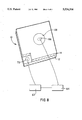
- the breakdown voltage of an anodized aluminum component 10 was determined utilizing the apparatus illustrated in FIG. 8.
- a power controller 63 was electrically interconnected in series with an amp meter 64.
- a first probe 66 was bonded to the anodic film 14 by a silver-filled epoxy resin 68. The area of contact between the silver-filled epoxy resin 68 and the anodic film 14 was accurately measured so that the area over which the voltage was applied could be accurately determined.
- a second probe 70 was electrically interconnected directly to the aluminum alloy core 12. The voltage provided by the power controller 62 was then gradually increased until the amp meter 64 registered current flow through the anodic film 14. The minimum voltage for current flow was the breakdown voltage.
- Table 1 compares the breakdown voltage of aluminum alloy components coated with a 0.025 mm (0.001 inch) anodic film formed by integral color anodization.
- the direct chill (D.C.) cast alloy A3003 had intermetallics with an average maximum axis length of 16 microns.
- the strip cast aluminum alloy A3003 had intermetallics with an average maximum axis length of 8 microns.
- the aluminum alloy A6061 was D.C. cast and had intermetallics that are substantially soluble in a sulfuric acid based electrolyte and the anodic film was essentially intermetallic free.
- Table 2 compares the breakdown voltage of two aluminum alloy 5252 components and illustrate the increased breakdown voltage achieved with a smoother core surface and hard anodization as compared to an integral color anodized aluminum alloy 6061 component.
- the bright roll sample was reduced to final gauge by passing through a pair of polished rolls in a rolling mill.
- the chemical polish sample was reduced to final gauge by passing through a pair of polished rolls in a rolling mill and then polished by immersion for 4 minutes in a solution of 95% by weight phosphoric acid, 5% nitric acid at a solution temperature of 95° C.-100° C.
- Table 3 illustrates how sealing the pores of an anodic film improves the breakdown voltage after subsequent processing, such as coating with a photoresist or metallization.
- the samples were then immersed in a 50% photoresist developing solution that contained a mixture of trisodium phosphate and sodium metasilicate at a pH of about 13 for 4 minutes.
- the samples were then water rinsed and dried in acetone.
- Table 4 illustrates the levelling effect of the dilute epoxy cresol novolac of the invention.
- the epoxy was diluted, by weight, in acetone to contain from 8.7%, by weight, solids up to 26% solids.
- Table 4 illustrates that excessive dilution negatively impacts the surface roughness and the sealing of the pores of the anodic film.
- Table 5 illustrates that the epoxy coating enhances both the breakdown voltage and the force required to separate an epoxy bonded stud from the substrate. This improvement is noted when comparing anodized A6061 to epoxy coated and anodized A6061. The improvement is also noted when comparing copper or nickel jet vapor deposited metallizations on anodized A6061 with the same metallizations on epoxy coated, anodized A6061. The improved adhesion of the metallized substrates noted for the jet vapor deposition process is believed to be equally applicable to other deposition processes such as sputtering, evaporation and the like.
Abstract
Description
______________________________________
Epoxy cresol novolac resin
                    33.5%
Cresol novolac hardener
                    15.2%
2 methyl imidizole  0.3%
Florad Surfactant   0.001%
Acetone             50.999%
______________________________________
              TABLE 1
______________________________________
            Measured Breakdown
                            Average Break-
Substrate   Voltage         down Voltage
______________________________________
D.C. Cast A3003
            10, 15, 71, 55, 71
                             37
            46, 17, 10
Strip Cast A3003
            193, 190, 126, 183,
                            148
            128, 136, 176, 207,
            220, 165, 226, 197,
            153, 110, 165, 187,
            140, 32, 10, 10
D.C. Cast A6061
            133, 450, 249, 186,
                            244
            351, 142, 84, 356, 289,
            157, 161, 180, 313,
            148, 163, 500, 170, 185
______________________________________
              TABLE 2
______________________________________
            Average    Maximum
            Surface    Surface    Breakdown
Alloy       Roughness  Roughness  Voltage
Condition   (micron)   (micron)   (volts)
______________________________________
Bright Roll - 5252
            0.21       1.88       930
Chemical Polish -
            0.11       0.97       >1000
5252
Integral Color -
            0.92       7.45       258
6061
______________________________________
              TABLE 3
______________________________________
Breakdown Voltage (volts)
                                    Anodized
                 Anodized   Anodized
                                    Sealed
Sample Anodized  Developed  Sealed  Developed
______________________________________
1      619       390        405     259
2      367       484        300     203
3      341       230        248     248
4      303       200        380     362
5      395       188        394     429
6      424       218        469     442
7      292       101        400     360
8      354       214        214     490
9      322       258        209     498
10     374       265        364     280
11     368       318        296     338
12     391       239        336     386
Average
       379       259        335     358
______________________________________
              TABLE 4
______________________________________
             Maximum       Average Surface
             Surface Roughness
                           Roughness
Substrate    Microns       Microns
______________________________________
Uncoated A6061
             33.7          3.36
Epoxy Coating (26%
             11.9          0.77
Solids) A6061
Epoxy Coating (13%
             29.0          3.24
Solids) A6061
Epoxy Coating (8.7%
             28.7          3.19
Solids) A6061
______________________________________
              TABLE 5
______________________________________
             Average              Average
             Breakdown            Pull Force
Substrate    Voltage    Coating   (pounds)
______________________________________
A6061        290        None      89
A6061 Epoxy coated
              600+      None      99
(26% solids)
A6061         63        Copper    87
A6061        174        Nickel    35
A6061 Epoxy coated
              600+      Copper    112
(26% solids)
A6061 Epoxy coated
             321        Nickel    68
(26% solids)
______________________________________
Claims (5)
Priority Applications (8)
| Application Number | Priority Date | Filing Date | Title |
|---|---|---|---|
| US08/427,921 US5534356A (en) | 1995-04-26 | 1995-04-26 | Anodized aluminum substrate having increased breakdown voltage |
| AU55385/96A AU5538596A (en) | 1995-04-26 | 1996-04-10 | Anodized aluminum substrate having increased breakdown volta ge |
| JP8532552A JPH11504387A (en) | 1995-04-26 | 1996-04-10 | Anodized aluminum substrate with high breakdown voltage |
| EP96912640A EP0822894A4 (en) | 1995-04-26 | 1996-04-10 | Anodized aluminum substrate having increased breakdown voltage |
| PCT/US1996/004875 WO1996033863A1 (en) | 1995-04-26 | 1996-04-10 | Anodized aluminum substrate having increased breakdown voltage |
| KR1019970707533A KR19990008009A (en) | 1995-04-26 | 1996-04-10 | Anodized aluminum substrate with increased breakdown voltage |
| US08/633,256 US5688606A (en) | 1995-04-26 | 1996-04-18 | Anodized aluminum substrate having increased breakdown voltage |
| TW085108311A TW324849B (en) | 1995-04-26 | 1996-07-09 | Anodized aluminum substrate having increased breakdown voltage |
Applications Claiming Priority (1)
| Application Number | Priority Date | Filing Date | Title |
|---|---|---|---|
| US08/427,921 US5534356A (en) | 1995-04-26 | 1995-04-26 | Anodized aluminum substrate having increased breakdown voltage |
Related Child Applications (1)
| Application Number | Title | Priority Date | Filing Date |
|---|---|---|---|
| US08/633,256 Division US5688606A (en) | 1995-04-26 | 1996-04-18 | Anodized aluminum substrate having increased breakdown voltage |
Publications (1)
| Publication Number | Publication Date |
|---|---|
| US5534356A true US5534356A (en) | 1996-07-09 |
Family
ID=23696850
Family Applications (2)
| Application Number | Title | Priority Date | Filing Date |
|---|---|---|---|
| US08/427,921 Expired - Fee Related US5534356A (en) | 1995-04-26 | 1995-04-26 | Anodized aluminum substrate having increased breakdown voltage |
| US08/633,256 Expired - Fee Related US5688606A (en) | 1995-04-26 | 1996-04-18 | Anodized aluminum substrate having increased breakdown voltage |
Family Applications After (1)
| Application Number | Title | Priority Date | Filing Date |
|---|---|---|---|
| US08/633,256 Expired - Fee Related US5688606A (en) | 1995-04-26 | 1996-04-18 | Anodized aluminum substrate having increased breakdown voltage |
Country Status (7)
| Country | Link |
|---|---|
| US (2) | US5534356A (en) |
| EP (1) | EP0822894A4 (en) |
| JP (1) | JPH11504387A (en) |
| KR (1) | KR19990008009A (en) |
| AU (1) | AU5538596A (en) |
| TW (1) | TW324849B (en) |
| WO (1) | WO1996033863A1 (en) |
Cited By (26)
| Publication number | Priority date | Publication date | Assignee | Title |
|---|---|---|---|---|
| WO1999005196A1 (en) * | 1997-07-24 | 1999-02-04 | Loctite Corporation | Thermosetting resin compositions useful as underfill sealants |
| US5952083A (en) * | 1997-10-21 | 1999-09-14 | Advanced Technology Interconnect, Inc. | Aluminum alloys for electronic components |
| GB2341566A (en) * | 1998-09-18 | 2000-03-22 | Lexmark Int Inc | Treating aluminum substrates |
| US6632893B2 (en) | 1999-05-28 | 2003-10-14 | Henkel Loctite Corporation | Composition of epoxy resin, cyanate ester, imidazole and polysulfide tougheners |
| EP1587348A1 (en) * | 2004-03-30 | 2005-10-19 | Feng Chia University | Conductive base board |
| US7208418B1 (en) * | 2003-12-08 | 2007-04-24 | Advanced Micro Devices, Inc. | Sealing sidewall pores in low-k dielectrics |
| US20070096658A1 (en) * | 2002-09-30 | 2007-05-03 | Tokyo Electron Limited | Method and apparatus for an improved upper electrode plate in a plasma processing system |
| US20070102287A1 (en) * | 2002-09-30 | 2007-05-10 | Tokyo Electron Limited | Method and apparatus for an improved optical window deposition shield in a plasma processing system |
| US20070142956A1 (en) * | 2003-03-31 | 2007-06-21 | Gary Escher | Method for adjoining adjacent coatings on a processing element |
| US20070257335A1 (en) * | 2004-10-29 | 2007-11-08 | O'brien Peter | Illuminator and Manufacturing Method |
| US7552521B2 (en) | 2004-12-08 | 2009-06-30 | Tokyo Electron Limited | Method and apparatus for improved baffle plate |
| US7566379B2 (en) | 2002-09-30 | 2009-07-28 | Tokyo Electron Limited | Method and apparatus for an improved upper electrode plate with deposition shield in a plasma processing system |
| US7601242B2 (en) | 2005-01-11 | 2009-10-13 | Tokyo Electron Limited | Plasma processing system and baffle assembly for use in plasma processing system |
| US7678226B2 (en) | 2002-09-30 | 2010-03-16 | Tokyo Electron Limited | Method and apparatus for an improved bellows shield in a plasma processing system |
| US7780786B2 (en) * | 2002-11-28 | 2010-08-24 | Tokyo Electron Limited | Internal member of a plasma processing vessel |
| US7846291B2 (en) | 1999-12-10 | 2010-12-07 | Tokyo Electron Limited | Processing apparatus with a chamber having therein a high-corrosion-resistant sprayed film |
| US7910223B2 (en) | 2003-07-17 | 2011-03-22 | Honeywell International Inc. | Planarization films for advanced microelectronic applications and devices and methods of production thereof |
| US8057600B2 (en) | 2002-09-30 | 2011-11-15 | Tokyo Electron Limited | Method and apparatus for an improved baffle plate in a plasma processing system |
| US8117986B2 (en) | 2002-09-30 | 2012-02-21 | Tokyo Electron Limited | Apparatus for an improved deposition shield in a plasma processing system |
| US8118936B2 (en) | 2002-09-30 | 2012-02-21 | Tokyo Electron Limited | Method and apparatus for an improved baffle plate in a plasma processing system |
| JP2013049903A (en) * | 2011-08-31 | 2013-03-14 | Kobe Steel Ltd | Method for manufacturing aluminum anodic oxide coating being superior in productivity and having high voltage endurance |
| US8580067B2 (en) * | 2012-02-23 | 2013-11-12 | Chroma Paper, Llc. | Thermo-sealing control method and packaging for resealable packaging |
| US20140218943A1 (en) * | 2013-02-01 | 2014-08-07 | Crystalplex Corporation | Aluminum printed circuit board for lighting and display backplanes |
| US20160172344A1 (en) * | 2014-12-16 | 2016-06-16 | Qualcomm Incorporated | Low profile reinforced package-on-package semiconductor device |
| US10539297B2 (en) | 2011-06-20 | 2020-01-21 | Crystalplex Corporation | Quantum dot containing light module |
| US11767608B2 (en) | 2017-03-06 | 2023-09-26 | Arconic Technologies Llc | Methods of preparing 7xxx aluminum alloys for adhesive bonding, and products relating to the same |
Families Citing this family (36)
| Publication number | Priority date | Publication date | Assignee | Title |
|---|---|---|---|---|
| US6248612B1 (en) * | 1997-06-20 | 2001-06-19 | Substrate Technologies, Inc. | Method for making a substrate for an integrated circuit package |
| US6465085B1 (en) * | 2000-04-04 | 2002-10-15 | Fujitsu Limited | Thin film wiring board and method for manufacturing the same, base substrate and method for manufacturing the same |
| JP2004534390A (en) | 2001-05-04 | 2004-11-11 | マイクロメタル テクノロジーズ インコーポレイテッド | Metallized dielectric substrate for EAS tags |
| US20030194545A1 (en) | 2002-04-11 | 2003-10-16 | Zesch James Charles | Systems and methods for filling voids and improving properties of porous thin films |
| US7113131B2 (en) * | 2002-05-02 | 2006-09-26 | Micrometal Technologies, Inc. | Metalized dielectric substrates for EAS tags |
| US20050051763A1 (en) * | 2003-09-05 | 2005-03-10 | Helicon Research, L.L.C. | Nanophase multilayer barrier and process |
| JP4808374B2 (en) * | 2003-11-13 | 2011-11-02 | 富士通株式会社 | Surface treatment method for metal molded products |
| US7036219B2 (en) * | 2004-04-01 | 2006-05-02 | Feng Chia University | Method for manufacturing a high-efficiency thermal conductive base board |
| US20060050492A1 (en) * | 2004-09-03 | 2006-03-09 | Staktek Group, L.P. | Thin module system and method |
| US7616452B2 (en) * | 2004-09-03 | 2009-11-10 | Entorian Technologies, Lp | Flex circuit constructions for high capacity circuit module systems and methods |
| US7423885B2 (en) | 2004-09-03 | 2008-09-09 | Entorian Technologies, Lp | Die module system |
| US7324352B2 (en) * | 2004-09-03 | 2008-01-29 | Staktek Group L.P. | High capacity thin module system and method |
| US7542297B2 (en) * | 2004-09-03 | 2009-06-02 | Entorian Technologies, Lp | Optimized mounting area circuit module system and method |
| US7760513B2 (en) | 2004-09-03 | 2010-07-20 | Entorian Technologies Lp | Modified core for circuit module system and method |
| US7511968B2 (en) * | 2004-09-03 | 2009-03-31 | Entorian Technologies, Lp | Buffered thin module system and method |
| US7443023B2 (en) | 2004-09-03 | 2008-10-28 | Entorian Technologies, Lp | High capacity thin module system |
| US7579687B2 (en) * | 2004-09-03 | 2009-08-25 | Entorian Technologies, Lp | Circuit module turbulence enhancement systems and methods |
| US7606050B2 (en) * | 2004-09-03 | 2009-10-20 | Entorian Technologies, Lp | Compact module system and method |
| KR100656295B1 (en) * | 2004-11-29 | 2006-12-11 | (주)웨이브닉스이에스피 | Fabrication method of package using a selectively anodized metal |
| GB2422249A (en) * | 2005-01-15 | 2006-07-19 | Robert John Morse | Power substrate |
| US20080062652A1 (en) * | 2006-09-07 | 2008-03-13 | Wayne Lieberman | Vapor heat spreader |
| US20080138538A1 (en) * | 2006-12-06 | 2008-06-12 | General Electric Company | Barrier layer, composite article comprising the same, electroactive device, and method |
| US8057883B2 (en) * | 2007-05-30 | 2011-11-15 | Kemet Electronics Corporation | Abrasive process for modifying corners, edges, and surfaces of capacitor anode bodies |
| KR100917841B1 (en) * | 2008-07-25 | 2009-09-18 | 코아셈(주) | Metal substrate for electronic components module and electronic components module using it and method of manufacturing metal substrate for electronic components module |
| KR100934476B1 (en) * | 2009-03-30 | 2009-12-30 | 코아셈(주) | Circuit board and method of manufacturing the same |
| KR20100125805A (en) * | 2009-05-21 | 2010-12-01 | 삼성전기주식회사 | Heat-dissipating substrate and fabricating method of the same |
| CN102666940A (en) | 2009-12-25 | 2012-09-12 | 富士胶片株式会社 | Insulated substrate, process for production of insulated substrate, process for formation of wiring line, wiring substrate, and light-emitting element |
| KR101109359B1 (en) * | 2010-06-14 | 2012-01-31 | 삼성전기주식회사 | Heat-radiating substrate and manufacturing method thereof |
| KR101156840B1 (en) * | 2010-07-01 | 2012-06-18 | 삼성전기주식회사 | Printed circuit board and the method of manufacturing thereof |
| KR101118846B1 (en) * | 2010-10-12 | 2012-03-14 | 삼성전기주식회사 | Heat radiating substrate and method of manufacturing the same |
| ES2638666T3 (en) * | 2011-02-08 | 2017-10-23 | Cambridge Nanolitic Limited | Non-metallic coating and production method |
| CN104185365B (en) * | 2013-05-23 | 2018-06-26 | 比亚迪股份有限公司 | A kind of wiring board and preparation method thereof |
| GB2521813A (en) * | 2013-11-15 | 2015-07-08 | Cambridge Nanotherm Ltd | Flexible electronic substrate |
| US20160014878A1 (en) * | 2014-04-25 | 2016-01-14 | Rogers Corporation | Thermal management circuit materials, method of manufacture thereof, and articles formed therefrom |
| US9842971B2 (en) * | 2014-09-24 | 2017-12-12 | Kyocera Corporation | Electronic component mounting substrate and light emission device using same |
| MX2019015390A (en) * | 2017-06-28 | 2020-02-20 | Arconic Tech Llc | Preparation methods for adhesive bonding of 7xxx aluminum alloys, and products relating to the same. |
Citations (26)
| Publication number | Priority date | Publication date | Assignee | Title |
|---|---|---|---|---|
| US4188652A (en) * | 1978-01-17 | 1980-02-12 | Smolko Gennady G | Electronic device |
| US4301765A (en) * | 1979-01-10 | 1981-11-24 | Siemens Aktiengesellschaft | Apparatus for generating layers on a carrier foil |
| US4491622A (en) * | 1982-04-19 | 1985-01-01 | Olin Corporation | Composites of glass-ceramic to metal seals and method of making the same |
| US4495378A (en) * | 1980-09-22 | 1985-01-22 | Siemens Aktiengesellschaft | Heat-removing circuit boards |
| US4499118A (en) * | 1982-02-03 | 1985-02-12 | General Electric Company | Method for coating with an atomizable material |
| US4570337A (en) * | 1982-04-19 | 1986-02-18 | Olin Corporation | Method of assembling a chip carrier |
| US4582556A (en) * | 1982-11-22 | 1986-04-15 | Olin Corporation | Adhesion primers for encapsulating epoxies |
| US4594770A (en) * | 1982-07-15 | 1986-06-17 | Olin Corporation | Method of making semiconductor casing |
| US4611745A (en) * | 1984-02-24 | 1986-09-16 | Kabushiki Kaisha Toshiba | Method for preparing highly heat-conductive substrate and copper wiring sheet usable in the same |
| US4682414A (en) * | 1982-08-30 | 1987-07-28 | Olin Corporation | Multi-layer circuitry |
| US4696851A (en) * | 1985-03-25 | 1987-09-29 | Olin Corporation | Hybrid and multi-layer circuitry |
| US4827377A (en) * | 1982-08-30 | 1989-05-02 | Olin Corporation | Multi-layer circuitry |
| US4842959A (en) * | 1986-10-17 | 1989-06-27 | The Furukawa Electric Co., Ltd. | Aluminum enamel board |
| US4853491A (en) * | 1984-10-03 | 1989-08-01 | Olin Corporation | Chip carrier |
| US4862323A (en) * | 1984-04-12 | 1989-08-29 | Olin Corporation | Chip carrier |
| US4866571A (en) * | 1982-06-21 | 1989-09-12 | Olin Corporation | Semiconductor package |
| US4888449A (en) * | 1988-01-04 | 1989-12-19 | Olin Corporation | Semiconductor package |
| US4939316A (en) * | 1988-10-05 | 1990-07-03 | Olin Corporation | Aluminum alloy semiconductor packages |
| US4953001A (en) * | 1985-09-27 | 1990-08-28 | Raytheon Company | Semiconductor device package and packaging method |
| US4967260A (en) * | 1988-05-04 | 1990-10-30 | International Electronic Research Corp. | Hermetic microminiature packages |
| US5013871A (en) * | 1988-02-10 | 1991-05-07 | Olin Corporation | Kit for the assembly of a metal electronic package |
| US5055967A (en) * | 1988-10-26 | 1991-10-08 | Texas Instruments Incorporated | Substrate for an electrical circuit system and a circuit system using that substrate |
| US5066368A (en) * | 1990-08-17 | 1991-11-19 | Olin Corporation | Process for producing black integrally colored anodized aluminum components |
| US5077595A (en) * | 1990-01-25 | 1991-12-31 | Mitsubishi Denki Kabushiki Kaisha | Semiconductor device |
| US5103292A (en) * | 1989-11-29 | 1992-04-07 | Olin Corporation | Metal pin grid array package |
| US5256205A (en) * | 1990-05-09 | 1993-10-26 | Jet Process Corporation | Microwave plasma assisted supersonic gas jet deposition of thin film materials |
Family Cites Families (9)
| Publication number | Priority date | Publication date | Assignee | Title |
|---|---|---|---|---|
| US3608191A (en) * | 1967-08-03 | 1971-09-28 | Lucas Industries Ltd | Semiconductor arrangements |
| GB2080630B (en) * | 1980-08-21 | 1985-07-10 | Ingram & Glass Ltd | Printed circuit panels |
| JPS59180832A (en) * | 1983-03-31 | 1984-10-15 | Nippon Light Metal Co Ltd | Alumite substrate for magnetic recording material |
| DE3667797D1 (en) * | 1985-10-30 | 1990-02-01 | Alusuisse | CARRIER FOR A LITHOGRAPHIC PRINT PLATE. |
| US4894126A (en) * | 1988-01-15 | 1990-01-16 | Mahmoud Issa S | Anodic coatings on aluminum for circuit packaging |
| JP2630858B2 (en) * | 1991-02-26 | 1997-07-16 | スカイアルミニウム株式会社 | Manufacturing method of printed wiring board |
| JPH06192778A (en) * | 1992-07-01 | 1994-07-12 | Sky Alum Co Ltd | Aluminum-based printed circuit board |
| JPH0645715A (en) * | 1992-07-22 | 1994-02-18 | Mitsui Toatsu Chem Inc | Wiring substrate |
| US5487218A (en) * | 1994-11-21 | 1996-01-30 | International Business Machines Corporation | Method for making printed circuit boards with selectivity filled plated through holes |
-
1995
- 1995-04-26 US US08/427,921 patent/US5534356A/en not_active Expired - Fee Related
-
1996
- 1996-04-10 AU AU55385/96A patent/AU5538596A/en not_active Abandoned
- 1996-04-10 KR KR1019970707533A patent/KR19990008009A/en not_active Application Discontinuation
- 1996-04-10 EP EP96912640A patent/EP0822894A4/en not_active Withdrawn
- 1996-04-10 WO PCT/US1996/004875 patent/WO1996033863A1/en not_active Application Discontinuation
- 1996-04-10 JP JP8532552A patent/JPH11504387A/en active Pending
- 1996-04-18 US US08/633,256 patent/US5688606A/en not_active Expired - Fee Related
- 1996-07-09 TW TW085108311A patent/TW324849B/en active
Patent Citations (26)
| Publication number | Priority date | Publication date | Assignee | Title |
|---|---|---|---|---|
| US4188652A (en) * | 1978-01-17 | 1980-02-12 | Smolko Gennady G | Electronic device |
| US4301765A (en) * | 1979-01-10 | 1981-11-24 | Siemens Aktiengesellschaft | Apparatus for generating layers on a carrier foil |
| US4495378A (en) * | 1980-09-22 | 1985-01-22 | Siemens Aktiengesellschaft | Heat-removing circuit boards |
| US4499118A (en) * | 1982-02-03 | 1985-02-12 | General Electric Company | Method for coating with an atomizable material |
| US4491622A (en) * | 1982-04-19 | 1985-01-01 | Olin Corporation | Composites of glass-ceramic to metal seals and method of making the same |
| US4570337A (en) * | 1982-04-19 | 1986-02-18 | Olin Corporation | Method of assembling a chip carrier |
| US4866571A (en) * | 1982-06-21 | 1989-09-12 | Olin Corporation | Semiconductor package |
| US4594770A (en) * | 1982-07-15 | 1986-06-17 | Olin Corporation | Method of making semiconductor casing |
| US4682414A (en) * | 1982-08-30 | 1987-07-28 | Olin Corporation | Multi-layer circuitry |
| US4827377A (en) * | 1982-08-30 | 1989-05-02 | Olin Corporation | Multi-layer circuitry |
| US4582556A (en) * | 1982-11-22 | 1986-04-15 | Olin Corporation | Adhesion primers for encapsulating epoxies |
| US4611745A (en) * | 1984-02-24 | 1986-09-16 | Kabushiki Kaisha Toshiba | Method for preparing highly heat-conductive substrate and copper wiring sheet usable in the same |
| US4862323A (en) * | 1984-04-12 | 1989-08-29 | Olin Corporation | Chip carrier |
| US4853491A (en) * | 1984-10-03 | 1989-08-01 | Olin Corporation | Chip carrier |
| US4696851A (en) * | 1985-03-25 | 1987-09-29 | Olin Corporation | Hybrid and multi-layer circuitry |
| US4953001A (en) * | 1985-09-27 | 1990-08-28 | Raytheon Company | Semiconductor device package and packaging method |
| US4842959A (en) * | 1986-10-17 | 1989-06-27 | The Furukawa Electric Co., Ltd. | Aluminum enamel board |
| US4888449A (en) * | 1988-01-04 | 1989-12-19 | Olin Corporation | Semiconductor package |
| US5013871A (en) * | 1988-02-10 | 1991-05-07 | Olin Corporation | Kit for the assembly of a metal electronic package |
| US4967260A (en) * | 1988-05-04 | 1990-10-30 | International Electronic Research Corp. | Hermetic microminiature packages |
| US4939316A (en) * | 1988-10-05 | 1990-07-03 | Olin Corporation | Aluminum alloy semiconductor packages |
| US5055967A (en) * | 1988-10-26 | 1991-10-08 | Texas Instruments Incorporated | Substrate for an electrical circuit system and a circuit system using that substrate |
| US5103292A (en) * | 1989-11-29 | 1992-04-07 | Olin Corporation | Metal pin grid array package |
| US5077595A (en) * | 1990-01-25 | 1991-12-31 | Mitsubishi Denki Kabushiki Kaisha | Semiconductor device |
| US5256205A (en) * | 1990-05-09 | 1993-10-26 | Jet Process Corporation | Microwave plasma assisted supersonic gas jet deposition of thin film materials |
| US5066368A (en) * | 1990-08-17 | 1991-11-19 | Olin Corporation | Process for producing black integrally colored anodized aluminum components |
Cited By (38)
| Publication number | Priority date | Publication date | Assignee | Title |
|---|---|---|---|---|
| AU728193B2 (en) * | 1997-07-24 | 2001-01-04 | Loctite Corporation | Thermosetting resin compositions useful as underfill sealants |
| US6342577B1 (en) | 1997-07-24 | 2002-01-29 | Loctite Corporation | Thermosetting resin compositions useful as underfill sealants |
| WO1999005196A1 (en) * | 1997-07-24 | 1999-02-04 | Loctite Corporation | Thermosetting resin compositions useful as underfill sealants |
| US5952083A (en) * | 1997-10-21 | 1999-09-14 | Advanced Technology Interconnect, Inc. | Aluminum alloys for electronic components |
| GB2341566A (en) * | 1998-09-18 | 2000-03-22 | Lexmark Int Inc | Treating aluminum substrates |
| US6410197B1 (en) | 1998-09-18 | 2002-06-25 | Lexmark International, Inc. | Methods for treating aluminum substrates and products thereof |
| GB2341566B (en) * | 1998-09-18 | 2002-09-18 | Lexmark Int Inc | Forming a photoconductor having a treated aluminium substrate |
| US6632893B2 (en) | 1999-05-28 | 2003-10-14 | Henkel Loctite Corporation | Composition of epoxy resin, cyanate ester, imidazole and polysulfide tougheners |
| US7846291B2 (en) | 1999-12-10 | 2010-12-07 | Tokyo Electron Limited | Processing apparatus with a chamber having therein a high-corrosion-resistant sprayed film |
| US7879179B2 (en) | 1999-12-10 | 2011-02-01 | Tokyo Electron Limited | Processing apparatus with a chamber having therein a high-corrosion-resistant sprayed film |
| US8117986B2 (en) | 2002-09-30 | 2012-02-21 | Tokyo Electron Limited | Apparatus for an improved deposition shield in a plasma processing system |
| US7566379B2 (en) | 2002-09-30 | 2009-07-28 | Tokyo Electron Limited | Method and apparatus for an improved upper electrode plate with deposition shield in a plasma processing system |
| US20070096658A1 (en) * | 2002-09-30 | 2007-05-03 | Tokyo Electron Limited | Method and apparatus for an improved upper electrode plate in a plasma processing system |
| US7811428B2 (en) | 2002-09-30 | 2010-10-12 | Tokyo Electron Limited | Method and apparatus for an improved optical window deposition shield in a plasma processing system |
| US8118936B2 (en) | 2002-09-30 | 2012-02-21 | Tokyo Electron Limited | Method and apparatus for an improved baffle plate in a plasma processing system |
| US7678226B2 (en) | 2002-09-30 | 2010-03-16 | Tokyo Electron Limited | Method and apparatus for an improved bellows shield in a plasma processing system |
| US7566368B2 (en) | 2002-09-30 | 2009-07-28 | Tokyo Electron Limited | Method and apparatus for an improved upper electrode plate in a plasma processing system |
| US20070102287A1 (en) * | 2002-09-30 | 2007-05-10 | Tokyo Electron Limited | Method and apparatus for an improved optical window deposition shield in a plasma processing system |
| US8057600B2 (en) | 2002-09-30 | 2011-11-15 | Tokyo Electron Limited | Method and apparatus for an improved baffle plate in a plasma processing system |
| US7780786B2 (en) * | 2002-11-28 | 2010-08-24 | Tokyo Electron Limited | Internal member of a plasma processing vessel |
| US8449715B2 (en) | 2002-11-28 | 2013-05-28 | Tokyo Electron Limited | Internal member of a plasma processing vessel |
| US20100307687A1 (en) * | 2002-11-28 | 2010-12-09 | Tokyo Electron Limited | Internal member of a plasma processing vessel |
| US8877002B2 (en) | 2002-11-28 | 2014-11-04 | Tokyo Electron Limited | Internal member of a plasma processing vessel |
| US7560376B2 (en) | 2003-03-31 | 2009-07-14 | Tokyo Electron Limited | Method for adjoining adjacent coatings on a processing element |
| US20070142956A1 (en) * | 2003-03-31 | 2007-06-21 | Gary Escher | Method for adjoining adjacent coatings on a processing element |
| US7910223B2 (en) | 2003-07-17 | 2011-03-22 | Honeywell International Inc. | Planarization films for advanced microelectronic applications and devices and methods of production thereof |
| US7208418B1 (en) * | 2003-12-08 | 2007-04-24 | Advanced Micro Devices, Inc. | Sealing sidewall pores in low-k dielectrics |
| EP1587348A1 (en) * | 2004-03-30 | 2005-10-19 | Feng Chia University | Conductive base board |
| US20070257335A1 (en) * | 2004-10-29 | 2007-11-08 | O'brien Peter | Illuminator and Manufacturing Method |
| US7552521B2 (en) | 2004-12-08 | 2009-06-30 | Tokyo Electron Limited | Method and apparatus for improved baffle plate |
| US7601242B2 (en) | 2005-01-11 | 2009-10-13 | Tokyo Electron Limited | Plasma processing system and baffle assembly for use in plasma processing system |
| US10539297B2 (en) | 2011-06-20 | 2020-01-21 | Crystalplex Corporation | Quantum dot containing light module |
| JP2013049903A (en) * | 2011-08-31 | 2013-03-14 | Kobe Steel Ltd | Method for manufacturing aluminum anodic oxide coating being superior in productivity and having high voltage endurance |
| US8580067B2 (en) * | 2012-02-23 | 2013-11-12 | Chroma Paper, Llc. | Thermo-sealing control method and packaging for resealable packaging |
| US20140218943A1 (en) * | 2013-02-01 | 2014-08-07 | Crystalplex Corporation | Aluminum printed circuit board for lighting and display backplanes |
| US20160172344A1 (en) * | 2014-12-16 | 2016-06-16 | Qualcomm Incorporated | Low profile reinforced package-on-package semiconductor device |
| US9875997B2 (en) * | 2014-12-16 | 2018-01-23 | Qualcomm Incorporated | Low profile reinforced package-on-package semiconductor device |
| US11767608B2 (en) | 2017-03-06 | 2023-09-26 | Arconic Technologies Llc | Methods of preparing 7xxx aluminum alloys for adhesive bonding, and products relating to the same |
Also Published As
| Publication number | Publication date |
|---|---|
| AU5538596A (en) | 1996-11-18 |
| EP0822894A1 (en) | 1998-02-11 |
| EP0822894A4 (en) | 2000-09-20 |
| KR19990008009A (en) | 1999-01-25 |
| WO1996033863A1 (en) | 1996-10-31 |
| JPH11504387A (en) | 1999-04-20 |
| TW324849B (en) | 1998-01-11 |
| US5688606A (en) | 1997-11-18 |
Similar Documents
| Publication | Publication Date | Title |
|---|---|---|
| US5534356A (en) | Anodized aluminum substrate having increased breakdown voltage | |
| EP0700083B1 (en) | Aluminium alloy base semiconductor packages | |
| JP3841768B2 (en) | Package parts and semiconductor packages | |
| US5917157A (en) | Multilayer wiring board laminate with enhanced thermal dissipation to dielectric substrate laminate | |
| US4888449A (en) | Semiconductor package | |
| US8866027B2 (en) | Printed wiring board and method for manufacturing the same | |
| KR101089201B1 (en) | Conductor substrate, semiconductor device and production method thereof | |
| US5540378A (en) | Method for the assembly of an electronic package | |
| JPS59104499A (en) | Copper foil treatment and laminate | |
| JP4698708B2 (en) | Package parts and semiconductor packages | |
| US5952083A (en) | Aluminum alloys for electronic components | |
| JP4628263B2 (en) | Package component, manufacturing method thereof, and semiconductor package | |
| US5573845A (en) | Superficial coating layer having acicular structures for electrical conductors | |
| JP2011071566A (en) | Package component and semiconductor package | |
| JPH06152087A (en) | High-cooling metal base printed wiring board | |
| JP3596563B2 (en) | Conductive paste | |
| JPH11286794A (en) | Surface treatment of copper or copper alloy material | |
| JPS6288399A (en) | Manufacture of integrated circuit substrate | |
| JPS63173389A (en) | Method of plating contact terminal of flexible printed wiring | |
| JP4307473B2 (en) | Conductor base material and semiconductor device manufacturing method | |
| JPS6213065B2 (en) | ||
| JPH0632353B2 (en) | Printed circuit board and manufacturing method thereof | |
| JPH06338216A (en) | Conductive paste | |
| JPH05114668A (en) | Aluminum substrate for semiconductor | |
| JPH0421358B2 (en) |
Legal Events
| Date | Code | Title | Description |
|---|---|---|---|
| AS | Assignment |
Owner name: OLIN CORPORATION, CONNECTICUT Free format text: ASSIGNMENT OF ASSIGNORS INTEREST;ASSIGNORS:MAHULIKAR, DEEPAK;SAGIV, EFRAIM;PARTHASARATHI, ARVIND;AND OTHERS;REEL/FRAME:007461/0324;SIGNING DATES FROM 19950404 TO 19950421 |
|
| FEPP | Fee payment procedure |
Free format text: PAYOR NUMBER ASSIGNED (ORIGINAL EVENT CODE: ASPN); ENTITY STATUS OF PATENT OWNER: LARGE ENTITY |
|
| AS | Assignment |
Owner name: ADVANCED TECHNOLOGY INTERCONNECT INCORPORATED, CAL Free format text: ASSIGNMENT OF ASSIGNORS INTEREST;ASSIGNOR:OLIN CORPORATION;REEL/FRAME:009781/0951 Effective date: 19990219 |
|
| REMI | Maintenance fee reminder mailed | ||
| LAPS | Lapse for failure to pay maintenance fees | ||
| FP | Lapsed due to failure to pay maintenance fee |
Effective date: 20000709 |
|
| STCH | Information on status: patent discontinuation |
Free format text: PATENT EXPIRED DUE TO NONPAYMENT OF MAINTENANCE FEES UNDER 37 CFR 1.362 |