US5521422A - Corner protected shallow trench isolation device - Google Patents
Corner protected shallow trench isolation device Download PDFInfo
- Publication number
- US5521422A US5521422A US08/348,709 US34870994A US5521422A US 5521422 A US5521422 A US 5521422A US 34870994 A US34870994 A US 34870994A US 5521422 A US5521422 A US 5521422A
- Authority
- US
- United States
- Prior art keywords
- corner
- trench
- dielectric
- insulator
- semiconductor structure
- Prior art date
- Legal status (The legal status is an assumption and is not a legal conclusion. Google has not performed a legal analysis and makes no representation as to the accuracy of the status listed.)
- Expired - Fee Related
Links
Images


Classifications
-
- H—ELECTRICITY
- H01—ELECTRIC ELEMENTS
- H01L—SEMICONDUCTOR DEVICES NOT COVERED BY CLASS H10
- H01L21/00—Processes or apparatus adapted for the manufacture or treatment of semiconductor or solid state devices or of parts thereof
- H01L21/70—Manufacture or treatment of devices consisting of a plurality of solid state components formed in or on a common substrate or of parts thereof; Manufacture of integrated circuit devices or of parts thereof
- H01L21/71—Manufacture of specific parts of devices defined in group H01L21/70
- H01L21/76—Making of isolation regions between components
- H01L21/762—Dielectric regions, e.g. EPIC dielectric isolation, LOCOS; Trench refilling techniques, SOI technology, use of channel stoppers
- H01L21/76224—Dielectric regions, e.g. EPIC dielectric isolation, LOCOS; Trench refilling techniques, SOI technology, use of channel stoppers using trench refilling with dielectric materials
Definitions
- This invention relates generally to semiconductor structures having a trench isolation. More particularly, it relates to field effect transistor devices adjacent a corner of a trench used for isolation and methods of avoiding corner parasitic leakage cement.
- Contemporary CMOS technologies employ field effect transistors that are adjacent or bounded by trenches.
- the trenches may provide isolation (shallow trench isolation, or STI) or they may provide a location for semiconductor devices, such as capacitors. Parasitic leakage paths have been found because of the proximity of a semiconductor device to an edge or corner of a trench.
- the parasitic leakage path results from an enhancement of the gate electric field near the trench corner.
- the electric field is enhanced by the corner's small radius of curvature and the proximity of the gate conductor. Processing can exacerbate the problem by sharpening the corner and thinning the gate dielectric near the corner.
- the gate conductor wraps around the trench corner. This happens when the oxide fill in the isolation trench is recessed below the silicon surface during oxide etches following its formation.
- the corner has a lower threshold voltage (Vt) than the planar portion of the device.
- Vt threshold voltage
- the top planar portion of the device carries most of the on-current.
- Trench corner conduction is a parasitic which usually contributes appreciably only to sub-threshold leakage. This parasitic leakage current along the corner is most easily seen as a hump in the subthreshold current curve of a narrow MOSFET.
- This paper teaches the use of a pair of aligned photomasks to form a T-shaped oxide adjacent the comet of an isolation trench and the use of a channel stop boron implant along sidewalls of the trench.
- the structure moves the device away from the trench sidewall and provides boron to raise the Vt along that sidewall.
- isolation is enlarged when photomask alignment tolerances are included in this two-mask-and-implant scheme, making this solution undesirable.
- an improved means to control the corner parasitic is needed and is provided by the following invention.
- a semiconductor structure comprising a semiconductor substrate having a planar surface.
- a trench having a sidewall is provided in the substrate.
- An intersection of the trench and the surface forms a corner.
- a dielectric lines the sidewall of the trench.
- a corner dielectric co-aligned with the corner extends no more than a subminimum dimension distance over the substrate from the corner.
- the corner dielectric is a spacer self-aligned to the edge of the trench dielectric.
- the corner dielectric is a spacer self-aligned to the edge of a window in insulator used as a mask to form the trench.
- this spacer defines the position of the trench, but the spacer is then removed. When the trench dielectric is later deposited, the trench dielectric forms the corner dielectric in the space provided by the removed spacer resulting in a unitary cap.
- Methods of fabricating a semiconductor structure of the invention comprise the steps of (a) providing a semiconductor substrate having a substantially planar surface; (b) forming a coating on the substrate; (c) forming a window in the coating, the window having an edge; (d) forming a trench in the substrate, the trench having a sidewall co-aligned to the edge, an intersection of the trench and the surface forming a corner; (e) lining the sidewall and the edge with insulator; and (f) forming a material on the substrate adjacent the corner, the material extending around the trench parallel to the corner and extending no more than a subminimum distance from the corner.
- FIGS. 1a-1e are cross sectional views showing the structure at several steps in the process for making a semiconductor structure of a first embodiment of the present invention
- FIG. 2 is a cross sectional view showing a structure illustrating how gate wrap around occurs with conventional processing
- FIG. 3a-3e are cross-sectional views showing the structure at several steps in the process for making a semiconductor structure of the second embodiment of the present invention.
- FIG. 4a-4c cross-sectional views showing the structure at several steps in the process for making a semiconductor structure of the third embodiment of the present invention
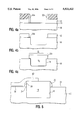
- FIG. 5 is cross-sectional view showing the structure of a MOSFET adjacent an isolation of the present invention.
- FIG. 6a is a simulation plot showing equipotential lines for a MOSFET adjacent an isolation with conventional geometry.
- FIG. 6b is a simulation plot showing equipotential lines for a MOSFET adjacent an isolation with the geometry of the present invention.
- the present invention provides a self-aligned structure over the corner that eliminates a recess formed in an adjacent insulator lined trench.
- trenches include shallow trench isolation (STI) and deep trench capacitor.
- STI and processes for forming STI are described in commonly assigned U.S. Pat. No. 5,173,439, by Dash et. al., incorporated herein by reference.
- the structure also offsets the gate conductor from the trench corner, further reducing the corner electric field.
- the modified gate conductor geometry results in an electric field at the trench corner that is actually lower than the field at the top planar region (see FIGS.
- GIDL gate induced drain leakage
- a corner dielectric is provided self-aligned to raised STI.
- the corner dielectric is a spacer that protects the STI corner from attack by subsequent etches and that spaces a later formed FET away from the corner.
- silicon substrate 10 is provided with a pad oxide 11 and nitride surface coating 12 as illustrated in FIG. 1a.
- Window 13 with nearly vertical sidewall 14 is photolithographically defined in surface coating 12 and oxide 11 as shown in FIG. 1b.
- trench 16 is etched, defined by window 13 as illustrated in FIG. 1c.
- Trench 16 and window 13 are then filled with insulator 18.
- Insulator 18 is then polished, stopping on surface coating 12 as illustrated in FIG. 1d. Then surface coating 12 is removed, leaving insulator 18 with nearly vertical sidewalls 20 extending above the surface 21 of silicon substrate 10.
- Spacer 22 is then provided self-aligned to sidewall 20 of insulator 18 by the standard process of depositing a spacer insulator having a desired thickness and directional etching to selectively remove the spacer insulator from horizontal surfaces.
- the spacer insulator can be a material such as CVD oxide, oxidized polysilicon, TEOS, silicon nitride, and boron nitride.
- Spacer 22 protects the STI adjacent corner 24 during subsequent etches, preventing divoting and gate wrap-around.
- spacer 22 has a dimension that is less than the minimum photolithographic dimension capable of being formed by a particular process technology.
- spacer 22 remains in place after subsequent etches, thereby also moving the gate controlled channel region of a later formed FET away from corner 24.
- high field effects including the corner parasitic FET and GIDL at the drain diffusion are eliminated.
- No additional photomasking is required for the formation of spacers 22, a significant advantage over the prior art.
- FIG. 2 illustrates a mechanism responsible for gate wrap-around and shows how the present invention eliminates this problem.
- Divot 30 in insulator 18 in trench 16 adjacent corner 24 arises during isotropic etches used in standard semiconductor processing after trench 16 is filled with insulator 18.
- Divot 30 is formed adjacent corner 24 as a result of the vertical and horizontal attack by etch ant on insulator at corner 24.
- etchant cannot access and form a recess or divot in insulator 18.
- a corner dielectric is also provided self-aligned to raised STI.
- the corner dielectric is again a spacer that protects the STI corner from attack by subsequent etches and that spaces a later formed FET away from the corner.
- the spacer is formed before the STI, it is inverted compared to the spacer of the first embodiment, and it is formed within the minimum dimension space of the isolation.
- no device area is consumed by the corner dielectric, a significant advantage.
- the RIE etching of the spacer does not effect the device region.
- silicon substrate 10 is again provided with nitride surface coating 12.
- Window 13 with nearly vertical sidewall 14 is again photolithographically defined in surface coating 12 as shown in FIG. 3a.
- spacer 22a is formed along sidewall 14 of coating 12.
- trench 16 is etched, defined by spacer 22a in window 13 as illustrated in FIG. 1c.
- trench 16 and window 13 are filled with insulator 18.
- Insulator 18 is then polished, stopping on surface coating 12.
- surface coating 12 is removed, leaving insulator 18 with spacer 22a extending above the surface 21 of silicon substrate 10.
- spacer 22a protects the STI adjacent corner 24 during subsequent etches, preventing divoting and gate wrap-around. Similarly, at least a portion of spacer 22a remains in place after subsequent etch steps, moving a later formed FET away from corner 24. And no additional photomasking is required for the formation of spacer 22a.
- This embodiment has a significant advantage over the first embodiment in that spacer 22a is within window 13, which can have a minimum dimension. Thus, spacer 22a does not take up device area, an advantage particularly for narrow devices such as DRAM cells.
- Trench 16 can have a dimension that is a subminimum dimension.
- a unitary structure having a corner dielectric co-aligned with the corner and extending a subminimum dimension distance over the substrate from the corner is provided.
- corner dielectric 22c is not itself a spacer but it fills the space left when previously formed spacer 22a is removed.
- This embodiment differs from the second embodiment in that spacer 22a of FIG. 3c is removed after trench 16 is etched as illustrated in FIG. 4b. Then, insulator 18a is deposited to fill both trench 16 and the space 22b left vacant by removed spacer 22a. After polishing, coating 12 is removed leaving a unitary raised STI structure having a subminimum dimension corner dielectric 22c, as illustrated in FIG. 4c.
- corner dielectric 22c and insulator 18a are formed of the same material. As with the second embodiment, corner dielectric 22c does not take up device area. Trench 16 can have a subminimum dimension while the isolation as a whole 32 covers no more than a minimum dimension. FIG. 4c also illustrates the formation of thermal oxide layer 34 before deposition of insulator 18a, as is well known in the art.
- a corner dielectric co-aligned with the corner means that the corner dielectric is aligned to an original edge to which the corner is also aligned (or either or both are aligned to an edge, such as a spacer edge, derived from the original edge).
- a trench having a sidewall co-aligned to an edge means that the sidewall is aligned to an original edge to which the edge is also aligned (or either or both are aligned to an edge, such as a spacer edge, derived from the original edge).
- a MOSFET can then formed bounded by a corner dielectric rather than the corner and sidewall of the STI.
- gate dielectric 38 is formed by conventional processing.
- Gate conductor 40 is then deposited and photolithographically defined. Gate conductor 40 is spaced from corner 24 by corner dielectric 22, 22a, or 22c. Thus, the electric field in the corner region is significantly reduced.
- FIGS. 6a-6b Device modeling, illustrated in FIGS. 6a-6b, shows that the modified geometry described here results in a drastic reduction of the trench corner electric field. Parasitic conduction and the GIDL concerns due to high corner fields are eliminated.
- the trench need not be filled with insulator.
- the insulator can be a thin lining along a sidewall or along the top portion of the sidewall.
Abstract
Description
Claims (10)
Priority Applications (2)
| Application Number | Priority Date | Filing Date | Title |
|---|---|---|---|
| US08/348,709 US5521422A (en) | 1994-12-02 | 1994-12-02 | Corner protected shallow trench isolation device |
| US08/604,283 US5741738A (en) | 1994-12-02 | 1996-02-21 | Method of making corner protected shallow trench field effect transistor |
Applications Claiming Priority (1)
| Application Number | Priority Date | Filing Date | Title |
|---|---|---|---|
| US08/348,709 US5521422A (en) | 1994-12-02 | 1994-12-02 | Corner protected shallow trench isolation device |
Related Child Applications (1)
| Application Number | Title | Priority Date | Filing Date |
|---|---|---|---|
| US08/604,283 Division US5741738A (en) | 1994-12-02 | 1996-02-21 | Method of making corner protected shallow trench field effect transistor |
Publications (1)
| Publication Number | Publication Date |
|---|---|
| US5521422A true US5521422A (en) | 1996-05-28 |
Family
ID=23369192
Family Applications (2)
| Application Number | Title | Priority Date | Filing Date |
|---|---|---|---|
| US08/348,709 Expired - Fee Related US5521422A (en) | 1994-12-02 | 1994-12-02 | Corner protected shallow trench isolation device |
| US08/604,283 Expired - Fee Related US5741738A (en) | 1994-12-02 | 1996-02-21 | Method of making corner protected shallow trench field effect transistor |
Family Applications After (1)
| Application Number | Title | Priority Date | Filing Date |
|---|---|---|---|
| US08/604,283 Expired - Fee Related US5741738A (en) | 1994-12-02 | 1996-02-21 | Method of making corner protected shallow trench field effect transistor |
Country Status (1)
| Country | Link |
|---|---|
| US (2) | US5521422A (en) |
Cited By (57)
| Publication number | Priority date | Publication date | Assignee | Title |
|---|---|---|---|---|
| EP0782185A3 (en) * | 1995-12-25 | 1997-08-20 | Nec Corp | Process of fabricating semiconductor device having isolating oxide rising out of groove |
| EP0884776A2 (en) * | 1997-06-11 | 1998-12-16 | Siemens Aktiengesellschaft | Isolation structure for DRAM cell with trench capacitor |
| EP0908948A2 (en) * | 1997-09-23 | 1999-04-14 | Siemens Aktiengesellschaft | Shallow trench isolation for DRAM trench capacitor |
| US5923991A (en) * | 1996-11-05 | 1999-07-13 | International Business Machines Corporation | Methods to prevent divot formation in shallow trench isolation areas |
| US5933748A (en) * | 1996-01-22 | 1999-08-03 | United Microelectronics Corp. | Shallow trench isolation process |
| US5940716A (en) * | 1996-03-15 | 1999-08-17 | Samsung Electronics Co., Ltd. | Methods of forming trench isolation regions using repatterned trench masks |
| US5960297A (en) * | 1997-07-02 | 1999-09-28 | Kabushiki Kaisha Toshiba | Shallow trench isolation structure and method of forming the same |
| US5981356A (en) * | 1997-07-28 | 1999-11-09 | Integrated Device Technology, Inc. | Isolation trenches with protected corners |
| US5989977A (en) * | 1998-04-20 | 1999-11-23 | Texas Instruments - Acer Incorporated | Shallow trench isolation process |
| US5998848A (en) * | 1998-09-18 | 1999-12-07 | International Business Machines Corporation | Depleted poly-silicon edged MOSFET structure and method |
| US6001706A (en) * | 1997-12-08 | 1999-12-14 | Chartered Semiconductor Manufacturing, Ltd. | Method for making improved shallow trench isolation for semiconductor integrated circuits |
| US6020621A (en) * | 1998-01-28 | 2000-02-01 | Texas Instruments - Acer Incorporated | Stress-free shallow trench isolation |
| US6025249A (en) * | 1997-09-10 | 2000-02-15 | United Microelectronics Corp. | Method for manufacturing shallow trench isolation structure |
| US6054343A (en) * | 1998-01-26 | 2000-04-25 | Texas Instruments Incorporated | Nitride trench fill process for increasing shallow trench isolation (STI) robustness |
| US6074932A (en) * | 1998-01-28 | 2000-06-13 | Texas Instruments - Acer Incorporated | Method for forming a stress-free shallow trench isolation |
| US6081662A (en) * | 1996-05-27 | 2000-06-27 | Mitsubishi Denki Kabushiki Kaisha | Semiconductor device including trench isolation structure and a method of manufacturing thereof |
| US6080637A (en) * | 1998-12-07 | 2000-06-27 | Taiwan Semiconductor Manufacturing Company | Shallow trench isolation technology to eliminate a kink effect |
| US6084276A (en) * | 1997-01-23 | 2000-07-04 | International Business Machines Corporation | Threshold voltage tailoring of corner of MOSFET device |
| US6091129A (en) * | 1996-06-19 | 2000-07-18 | Cypress Semiconductor Corporation | Self-aligned trench isolated structure |
| US6093619A (en) * | 1998-06-18 | 2000-07-25 | Taiwan Semiconductor Manufaturing Company | Method to form trench-free buried contact in process with STI technology |
| US6097069A (en) * | 1998-06-22 | 2000-08-01 | International Business Machines Corporation | Method and structure for increasing the threshold voltage of a corner device |
| US6103581A (en) * | 1998-11-27 | 2000-08-15 | Taiwan Semiconductor Manufacturing Company | Method for producing shallow trench isolation structure |
| US6121113A (en) * | 1997-06-30 | 2000-09-19 | Fujitsu Limited | Method for production of semiconductor device |
| US6147394A (en) * | 1997-07-17 | 2000-11-14 | International Business Machines Corporation | Method of photolithographically defining three regions with one mask step and self aligned isolation structure formed thereby |
| US6150273A (en) * | 1998-08-28 | 2000-11-21 | United Microelectronics Inc. | Method of fabricating a kink-effect-free shallow trench isolations |
| US6165854A (en) * | 1998-05-04 | 2000-12-26 | Texas Instruments - Acer Incorporated | Method to form shallow trench isolation with an oxynitride buffer layer |
| US6180491B1 (en) * | 1996-12-13 | 2001-01-30 | Texas Instruments Incorporated | Isolation structure and method |
| US6184106B1 (en) * | 1996-06-27 | 2001-02-06 | Hyundai Electronics Industries Co., Ltd. | Method for manufacturing a semiconductor device |
| US6187651B1 (en) | 1998-05-07 | 2001-02-13 | Samsung Electronics Co., Ltd. | Methods of forming trench isolation regions using preferred stress relieving layers and techniques to inhibit the occurrence of voids |
| US6194285B1 (en) | 1999-10-04 | 2001-02-27 | Taiwan Semiconductor Manufacturing Company | Formation of shallow trench isolation (STI) |
| US6228745B1 (en) | 1997-03-12 | 2001-05-08 | International Business Machines Corporation | Selective reduction of sidewall slope on isolation edge |
| US6251746B1 (en) | 1998-10-09 | 2001-06-26 | Samsung Electronics Co., Ltd. | Methods of forming trench isolation regions having stress-reducing nitride layers therein |
| US6281562B1 (en) * | 1995-07-27 | 2001-08-28 | Matsushita Electric Industrial Co., Ltd. | Semiconductor device which reduces the minimum distance requirements between active areas |
| US6319794B1 (en) | 1998-10-14 | 2001-11-20 | International Business Machines Corporation | Structure and method for producing low leakage isolation devices |
| US6322634B1 (en) | 1997-01-27 | 2001-11-27 | Micron Technology, Inc. | Shallow trench isolation structure without corner exposure |
| US20010046753A1 (en) * | 1997-03-25 | 2001-11-29 | Fernando Gonzalez | Method for forming a self-aligned isolation trench |
| US6331469B1 (en) | 1999-10-12 | 2001-12-18 | Samsung Electronics Co., Ltd. | Trench isolation structure, semiconductor device having the same, and trench isolation method |
| US6339018B1 (en) | 2000-03-09 | 2002-01-15 | International Business Machines Corporation | Silicide block bounded device |
| US6358818B1 (en) | 1998-03-04 | 2002-03-19 | Taiwan Semiconductor Manufacturing Co., Ltd. | Method for forming trench isolation regions |
| US6461937B1 (en) | 1999-01-11 | 2002-10-08 | Samsung Electronics Co., Ltd. | Methods of forming trench isolation regions having recess-inhibiting layers therein that protect against overetching |
| US6461935B2 (en) * | 1999-01-14 | 2002-10-08 | Mitsubishi Denki Kabushiki Kaisha | Method of manufacturing trench-shaped isolator |
| US6518145B1 (en) | 1998-08-06 | 2003-02-11 | International Business Machines Corporation | Methods to control the threshold voltage of a deep trench corner device |
| US6566224B1 (en) | 1997-07-31 | 2003-05-20 | Agere Systems, Inc. | Process for device fabrication |
| US20040067620A1 (en) * | 2002-10-02 | 2004-04-08 | Freidoon Mehrad | Method for moat nitride pull back for shallow trench isolation |
| US20040121532A1 (en) * | 2002-12-20 | 2004-06-24 | Young-Hun Seo | Trench in semiconductor device and formation method thereof |
| US6821857B1 (en) | 2003-06-10 | 2004-11-23 | International Business Machines Corporation | High on-current device for high performance embedded DRAM (eDRAM) and method of forming the same |
| US20050006795A1 (en) * | 2003-07-09 | 2005-01-13 | Cheng-Ming Yih | Corner free structure of nonvolatile memory |
| US20050196913A1 (en) * | 2002-10-07 | 2005-09-08 | Promos Technologies Inc. | Floating gate memory structures and fabrication methods |
| US20050224907A1 (en) * | 2003-08-15 | 2005-10-13 | Chih-Hsin Ko | Isolation structure with nitrogen-containing liner and methods of manufacture |
| US7129149B1 (en) | 2004-06-07 | 2006-10-31 | Integrated Device Technology, Inc. | Method for forming shallow trench isolation structure with anti-reflective liner |
| US7176104B1 (en) | 2004-06-08 | 2007-02-13 | Integrated Device Technology, Inc. | Method for forming shallow trench isolation structure with deep oxide region |
| US20070048916A1 (en) * | 2005-08-23 | 2007-03-01 | Fujitsu Limited | Method for fabricating semiconductor device |
| US20070087517A1 (en) * | 2005-10-13 | 2007-04-19 | Dongbuanam Semiconductor Inc. | Method of manufacturing semiconductor device |
| US20080166853A1 (en) * | 2006-12-28 | 2008-07-10 | Spansion Llc | Method for manufacturing a semiconductor device |
| US20110115044A1 (en) * | 2009-11-18 | 2011-05-19 | International Business Machines Corporation | Diffusion sidewall for a semiconductor structure |
| US9293557B2 (en) | 2014-02-20 | 2016-03-22 | International Business Machines Corporation | Low temperature spacer for advanced semiconductor devices |
| US20170358689A1 (en) * | 2015-12-18 | 2017-12-14 | International Business Machines Corporation | Vertical transistor fabrication and devices |
Families Citing this family (26)
| Publication number | Priority date | Publication date | Assignee | Title |
|---|---|---|---|---|
| JP4138035B2 (en) * | 1996-08-23 | 2008-08-20 | 株式会社東芝 | Semiconductor device |
| US5981332A (en) * | 1997-09-30 | 1999-11-09 | Siemens Aktiengesellschaft | Reduced parasitic leakage in semiconductor devices |
| JPH11111710A (en) * | 1997-10-01 | 1999-04-23 | Nec Corp | Semiconductor device and its manufacture |
| WO1999059202A1 (en) * | 1998-05-08 | 1999-11-18 | Advanced Micro Devices, Inc. | Method of forming a field isolation structure in a semiconductor substrate |
| US6165906A (en) * | 1999-01-26 | 2000-12-26 | Advanced Micro Devices, Inc. | Semiconductor topography employing a shallow trench isolation structure with an improved trench edge |
| US6388303B1 (en) * | 1999-04-21 | 2002-05-14 | Sanyo Electric Co., Ltd. | Semiconductor device and semiconductor device manufacture method |
| US6365946B1 (en) * | 1999-05-13 | 2002-04-02 | Stmicroelectronics, Inc. | Integrated-circuit isolation structure and method for forming the same |
| US6190961B1 (en) | 1999-09-22 | 2001-02-20 | International Business Machines Corporation | Fabricating a square spacer |
| US6251747B1 (en) * | 1999-11-02 | 2001-06-26 | Philips Semiconductors, Inc. | Use of an insulating spacer to prevent threshold voltage roll-off in narrow devices |
| US6207513B1 (en) | 1999-11-02 | 2001-03-27 | Infineon Technologies North America Corp. | Spacer process to eliminate corner transistor device |
| US6683345B1 (en) | 1999-12-20 | 2004-01-27 | International Business Machines, Corp. | Semiconductor device and method for making the device having an electrically modulated conduction channel |
| US6413828B1 (en) | 2000-03-08 | 2002-07-02 | International Business Machines Corporation | Process using poly-buffered STI |
| US6472274B1 (en) | 2000-06-29 | 2002-10-29 | International Business Machines Corporation | MOSFET with self-aligned channel edge implant and method |
| US6265285B1 (en) * | 2000-10-25 | 2001-07-24 | Vanguard International Semiconductor Corporation | Method of forming a self-aligned trench isolation |
| US6524938B1 (en) | 2002-02-13 | 2003-02-25 | Taiwan Semiconductor Manufacturing Company | Method for gate formation with improved spacer profile control |
| DE10329212B4 (en) * | 2003-06-28 | 2006-07-06 | Infineon Technologies Ag | Method for producing an integrated DRAM memory circuit with corner devices |
| US6864148B1 (en) | 2003-09-05 | 2005-03-08 | Mosel Vitelic, Inc. | Corner protection to reduce wrap around |
| US7242239B2 (en) * | 2005-06-07 | 2007-07-10 | International Business Machines Corporation | Programming and determining state of electrical fuse using field effect transistor having multiple conduction states |
| US8405165B2 (en) * | 2005-06-07 | 2013-03-26 | International Business Machines Corporation | Field effect transistor having multiple conduction states |
| US7123529B1 (en) | 2005-06-07 | 2006-10-17 | International Business Machines Corporation | Sense amplifier including multiple conduction state field effect transistor |
| US7768041B2 (en) * | 2006-06-21 | 2010-08-03 | International Business Machines Corporation | Multiple conduction state devices having differently stressed liners |
| US20090098702A1 (en) * | 2007-10-16 | 2009-04-16 | Texas Instruments Incorporated | Method to Form CMOS Circuits Using Optimized Sidewalls |
| US8546219B2 (en) | 2011-10-13 | 2013-10-01 | International Business Machines Corporation | Reducing performance variation of narrow channel devices |
| US20150050792A1 (en) * | 2013-08-13 | 2015-02-19 | Globalfoundries Inc. | Extra narrow diffusion break for 3d finfet technologies |
| US9735245B2 (en) | 2014-08-25 | 2017-08-15 | Taiwan Semiconductor Manufacturing Co., Ltd. | Recessed salicide structure to integrate a flash memory device with a high κ, metal gate logic device |
| US9431413B2 (en) * | 2014-11-19 | 2016-08-30 | Taiwan Semiconductor Manufacturing Co., Ltd. | STI recess method to embed NVM memory in HKMG replacement gate technology |
Citations (19)
| Publication number | Priority date | Publication date | Assignee | Title |
|---|---|---|---|---|
| US4389294A (en) * | 1981-06-30 | 1983-06-21 | International Business Machines Corporation | Method for avoiding residue on a vertical walled mesa |
| US4502913A (en) * | 1982-06-30 | 1985-03-05 | International Business Machines Corporation | Total dielectric isolation for integrated circuits |
| US4506434A (en) * | 1981-09-10 | 1985-03-26 | Fujitsu Limited | Method for production of semiconductor devices |
| US4814840A (en) * | 1985-08-09 | 1989-03-21 | Masahiro Kameda | High-density reprogrammable semiconductor memory device |
| US4836885A (en) * | 1988-05-03 | 1989-06-06 | International Business Machines Corporation | Planarization process for wide trench isolation |
| US4873203A (en) * | 1987-07-27 | 1989-10-10 | Hitachi, Ltd. | Method for formation of insulation film on silicon buried in trench |
| US4966870A (en) * | 1988-04-14 | 1990-10-30 | International Business Machines Corporation | Method for making borderless contacts |
| EP0401537A2 (en) * | 1989-05-14 | 1990-12-12 | Texas Instruments Incorporated | High density dynamic ram cell |
| US4988637A (en) * | 1990-06-29 | 1991-01-29 | International Business Machines Corp. | Method for fabricating a mesa transistor-trench capacitor memory cell structure |
| US4998161A (en) * | 1988-12-08 | 1991-03-05 | Mitsubishi Denki Kabushiki Kaisha | LDD MOS device having an element separation region having an electrostatic screening electrode |
| US5064777A (en) * | 1990-06-28 | 1991-11-12 | International Business Machines Corporation | Fabrication method for a double trench memory cell device |
| JPH0456279A (en) * | 1990-06-25 | 1992-02-24 | Matsushita Electron Corp | Manufacture of semiconductor device |
| US5160988A (en) * | 1988-08-03 | 1992-11-03 | Kabushiki Kaisha Toshiba | Semiconductor device with composite surface insulator |
| US5173439A (en) * | 1989-10-25 | 1992-12-22 | International Business Machines Corporation | Forming wide dielectric-filled isolation trenches in semi-conductors |
| US5250831A (en) * | 1990-03-28 | 1993-10-05 | Mitsubishi Denki Kabushiki Kaisha | DRAM device having a memory cell array of a divided bit line type |
| US5260588A (en) * | 1991-05-21 | 1993-11-09 | Eastman Kodak Company | Light-emitting diode array |
| US5275965A (en) * | 1992-11-25 | 1994-01-04 | Micron Semiconductor, Inc. | Trench isolation using gated sidewalls |
| US5292670A (en) * | 1991-06-10 | 1994-03-08 | Texas Instruments Incorporated | Sidewall doping technique for SOI transistors |
| US5298434A (en) * | 1992-02-07 | 1994-03-29 | Harris Corporation | Selective recrystallization to reduce P-channel transistor leakage in silicon-on-sapphire CMOS radiation hardened integrated circuits |
Family Cites Families (16)
| Publication number | Priority date | Publication date | Assignee | Title |
|---|---|---|---|---|
| JPS5683036A (en) * | 1979-12-12 | 1981-07-07 | Toshiba Corp | Glass passivation of mesa type semiconductor device |
| JPS57112047A (en) * | 1980-12-29 | 1982-07-12 | Fujitsu Ltd | Manufacture of semiconductor device |
| JPS5743431A (en) * | 1981-07-09 | 1982-03-11 | Toshiba Corp | Manufacture of semiconductor device |
| JPH0665225B2 (en) * | 1984-01-13 | 1994-08-22 | 株式会社東芝 | Method of manufacturing semiconductor memory device |
| US4589193A (en) * | 1984-06-29 | 1986-05-20 | International Business Machines Corporation | Metal silicide channel stoppers for integrated circuits and method for making the same |
| US4654120A (en) * | 1985-10-31 | 1987-03-31 | International Business Machines Corporation | Method of making a planar trench semiconductor structure |
| US5059550A (en) * | 1988-10-25 | 1991-10-22 | Sharp Kabushiki Kaisha | Method of forming an element isolating portion in a semiconductor device |
| JPH02294031A (en) * | 1989-05-09 | 1990-12-05 | Matsushita Electron Corp | Formation of trench |
| JPH03101147A (en) * | 1989-09-13 | 1991-04-25 | Toshiba Corp | Manufacture of semiconductor device |
| US5290396A (en) * | 1991-06-06 | 1994-03-01 | Lsi Logic Corporation | Trench planarization techniques |
| FR2683944B1 (en) * | 1991-11-14 | 1994-02-18 | Sgs Thomson Microelectronics Sa | PROCESS OF ENGRAVING A DEEP Furrow. |
| US5229316A (en) * | 1992-04-16 | 1993-07-20 | Micron Technology, Inc. | Semiconductor processing method for forming substrate isolation trenches |
| JP3311044B2 (en) * | 1992-10-27 | 2002-08-05 | 株式会社東芝 | Method for manufacturing semiconductor device |
| JPH07105438B2 (en) * | 1993-01-05 | 1995-11-13 | 日本電気株式会社 | Method for manufacturing semiconductor device |
| US5292683A (en) * | 1993-06-09 | 1994-03-08 | Micron Semiconductor, Inc. | Method of isolating semiconductor devices and arrays of memory integrated circuitry |
| JPH07326663A (en) * | 1994-05-31 | 1995-12-12 | Fuji Electric Co Ltd | Dielectric isolation method of wafer |
-
1994
- 1994-12-02 US US08/348,709 patent/US5521422A/en not_active Expired - Fee Related
-
1996
- 1996-02-21 US US08/604,283 patent/US5741738A/en not_active Expired - Fee Related
Patent Citations (19)
| Publication number | Priority date | Publication date | Assignee | Title |
|---|---|---|---|---|
| US4389294A (en) * | 1981-06-30 | 1983-06-21 | International Business Machines Corporation | Method for avoiding residue on a vertical walled mesa |
| US4506434A (en) * | 1981-09-10 | 1985-03-26 | Fujitsu Limited | Method for production of semiconductor devices |
| US4502913A (en) * | 1982-06-30 | 1985-03-05 | International Business Machines Corporation | Total dielectric isolation for integrated circuits |
| US4814840A (en) * | 1985-08-09 | 1989-03-21 | Masahiro Kameda | High-density reprogrammable semiconductor memory device |
| US4873203A (en) * | 1987-07-27 | 1989-10-10 | Hitachi, Ltd. | Method for formation of insulation film on silicon buried in trench |
| US4966870A (en) * | 1988-04-14 | 1990-10-30 | International Business Machines Corporation | Method for making borderless contacts |
| US4836885A (en) * | 1988-05-03 | 1989-06-06 | International Business Machines Corporation | Planarization process for wide trench isolation |
| US5160988A (en) * | 1988-08-03 | 1992-11-03 | Kabushiki Kaisha Toshiba | Semiconductor device with composite surface insulator |
| US4998161A (en) * | 1988-12-08 | 1991-03-05 | Mitsubishi Denki Kabushiki Kaisha | LDD MOS device having an element separation region having an electrostatic screening electrode |
| EP0401537A2 (en) * | 1989-05-14 | 1990-12-12 | Texas Instruments Incorporated | High density dynamic ram cell |
| US5173439A (en) * | 1989-10-25 | 1992-12-22 | International Business Machines Corporation | Forming wide dielectric-filled isolation trenches in semi-conductors |
| US5250831A (en) * | 1990-03-28 | 1993-10-05 | Mitsubishi Denki Kabushiki Kaisha | DRAM device having a memory cell array of a divided bit line type |
| JPH0456279A (en) * | 1990-06-25 | 1992-02-24 | Matsushita Electron Corp | Manufacture of semiconductor device |
| US5064777A (en) * | 1990-06-28 | 1991-11-12 | International Business Machines Corporation | Fabrication method for a double trench memory cell device |
| US4988637A (en) * | 1990-06-29 | 1991-01-29 | International Business Machines Corp. | Method for fabricating a mesa transistor-trench capacitor memory cell structure |
| US5260588A (en) * | 1991-05-21 | 1993-11-09 | Eastman Kodak Company | Light-emitting diode array |
| US5292670A (en) * | 1991-06-10 | 1994-03-08 | Texas Instruments Incorporated | Sidewall doping technique for SOI transistors |
| US5298434A (en) * | 1992-02-07 | 1994-03-29 | Harris Corporation | Selective recrystallization to reduce P-channel transistor leakage in silicon-on-sapphire CMOS radiation hardened integrated circuits |
| US5275965A (en) * | 1992-11-25 | 1994-01-04 | Micron Semiconductor, Inc. | Trench isolation using gated sidewalls |
Non-Patent Citations (14)
| Title |
|---|
| A. Bryant et al., "The Current-Carrying Corner Inherent to Trench Isolation", IEEE Electron Device Letters, vol. 14, No. 8, Aug. 1993, pp. 412-414. |
| A. Bryant et al., The Current Carrying Corner Inherent to Trench Isolation , IEEE Electron Device Letters, vol. 14, No. 8, Aug. 1993, pp. 412 414. * |
| C. W. Kaanta et al, "Use of Easily Removable Sacrificial Layer to Suppress Chemical-Mechanical Overpolish Damage", IBM Technical Disclosure Bulletin, vol. 34, No. 4B, pp. 343-344, Sep. 1991. |
| C. W. Kaanta et al, Use of Easily Removable Sacrificial Layer to Suppress Chemical Mechanical Overpolish Damage , IBM Technical Disclosure Bulletin, vol. 34, No. 4B, pp. 343 344, Sep. 1991. * |
| D. Foty et al., "Behavior of an NMOS Trench-Isolated Corner Parasitic Devide at Low Temperature", Proceedings of the Electrochemical Society Meeting, Oct. 1989, pp. 1-2. |
| D. Foty et al., Behavior of an NMOS Trench Isolated Corner Parasitic Devide at Low Temperature , Proceedings of the Electrochemical Society Meeting, Oct. 1989, pp. 1 2. * |
| J. F. Shepard, "Method to Reduce Loss of Isolation Trench Insulation", IBM Technical Disclosure Bulletin, vol. 33, No. 10A, pp. 298-299, Mar. 1991. |
| J. F. Shepard, Method to Reduce Loss of Isolation Trench Insulation , IBM Technical Disclosure Bulletin, vol. 33, No. 10A, pp. 298 299, Mar. 1991. * |
| P. C. Fazan et al., "A Highly Manufacturable Trench Isolation Process for Deep Submicron DRAMs", Proceedings of the IEDM, 1993, pp. 57-60. |
| P. C. Fazan et al., A Highly Manufacturable Trench Isolation Process for Deep Submicron DRAMs , Proceedings of the IEDM, 1993, pp. 57 60. * |
| T. Furukawa et al., "Process and Device Simulation of Trench Isolation Corner Parasitic Device", Procedings of the Electrochemical Society Meeting, Oct. 9-14, 1988, pp. 1-2. |
| T. Furukawa et al., Process and Device Simulation of Trench Isolation Corner Parasitic Device , Procedings of the Electrochemical Society Meeting, Oct. 9 14, 1988, pp. 1 2. * |
| T. Ishijima et al., "A Deep-Submicron Isolation Technology with T-shaped Oxide (TSO) Structure", Proceedings of the IEDM, 1990, pp. 257-260. |
| T. Ishijima et al., A Deep Submicron Isolation Technology with T shaped Oxide (TSO) Structure , Proceedings of the IEDM, 1990, pp. 257 260. * |
Cited By (92)
| Publication number | Priority date | Publication date | Assignee | Title |
|---|---|---|---|---|
| US6967409B2 (en) | 1995-07-27 | 2005-11-22 | Matsushita Electric Industrial Co., Ltd. | Semiconductor device and method of manufacturing the same |
| US20030205820A1 (en) * | 1995-07-27 | 2003-11-06 | Matsushita Electric Industrial Co., Ltd. | Semiconductor device and method of manufacturing the same |
| US6709950B2 (en) * | 1995-07-27 | 2004-03-23 | Matsushita Electric Industrial Co., Ltd. | Semiconductor device and method of manufacturing the same |
| US20050093089A1 (en) * | 1995-07-27 | 2005-05-05 | Matsushita Electric Industrial Co., Ltd. | Semiconductor device and method of manufacturing the same |
| US20050156220A1 (en) * | 1995-07-27 | 2005-07-21 | Matsushita Electric Industrial Co., Ltd. | Semiconductor device and method of manufacturing the same |
| US6281562B1 (en) * | 1995-07-27 | 2001-08-28 | Matsushita Electric Industrial Co., Ltd. | Semiconductor device which reduces the minimum distance requirements between active areas |
| US7126174B2 (en) | 1995-07-27 | 2006-10-24 | Matsushita Electric Industrial Co., Ltd. | Semiconductor device and method of manufacturing the same |
| EP0782185A3 (en) * | 1995-12-25 | 1997-08-20 | Nec Corp | Process of fabricating semiconductor device having isolating oxide rising out of groove |
| US5933748A (en) * | 1996-01-22 | 1999-08-03 | United Microelectronics Corp. | Shallow trench isolation process |
| US5940716A (en) * | 1996-03-15 | 1999-08-17 | Samsung Electronics Co., Ltd. | Methods of forming trench isolation regions using repatterned trench masks |
| US6081662A (en) * | 1996-05-27 | 2000-06-27 | Mitsubishi Denki Kabushiki Kaisha | Semiconductor device including trench isolation structure and a method of manufacturing thereof |
| US6091129A (en) * | 1996-06-19 | 2000-07-18 | Cypress Semiconductor Corporation | Self-aligned trench isolated structure |
| US6184106B1 (en) * | 1996-06-27 | 2001-02-06 | Hyundai Electronics Industries Co., Ltd. | Method for manufacturing a semiconductor device |
| US5923991A (en) * | 1996-11-05 | 1999-07-13 | International Business Machines Corporation | Methods to prevent divot formation in shallow trench isolation areas |
| US6180491B1 (en) * | 1996-12-13 | 2001-01-30 | Texas Instruments Incorporated | Isolation structure and method |
| US6084276A (en) * | 1997-01-23 | 2000-07-04 | International Business Machines Corporation | Threshold voltage tailoring of corner of MOSFET device |
| US6322634B1 (en) | 1997-01-27 | 2001-11-27 | Micron Technology, Inc. | Shallow trench isolation structure without corner exposure |
| US20020003277A1 (en) * | 1997-01-27 | 2002-01-10 | Pai-Hung Pan | Technique for forming shallow trench isolation structure without corner exposure and resulting structure |
| US8637956B2 (en) * | 1997-01-27 | 2014-01-28 | Micron Technology, Inc. | Semiconductor devices structures including an isolation structure |
| US20130001737A1 (en) * | 1997-01-27 | 2013-01-03 | Micron Technology, Inc. | Semiconductor devices structures including an isolation structure |
| US20110129985A1 (en) * | 1997-01-27 | 2011-06-02 | Micron Technology, Inc. | Methods for forming isolation structures for semiconductor devices |
| US7892941B2 (en) | 1997-01-27 | 2011-02-22 | Micron Technology, Inc. | Technique for forming shallow trench isolation structure without corner exposure |
| US8338264B2 (en) | 1997-01-27 | 2012-12-25 | Micron Technology, Inc. | Methods for forming isolation structures for semiconductor devices |
| US6228745B1 (en) | 1997-03-12 | 2001-05-08 | International Business Machines Corporation | Selective reduction of sidewall slope on isolation edge |
| US8173517B2 (en) | 1997-03-25 | 2012-05-08 | Micron Technology, Inc. | Method for forming a self-aligned isolation structure utilizing sidewall spacers as an etch mask and remaining as a portion of the isolation structure |
| US7749860B2 (en) * | 1997-03-25 | 2010-07-06 | Micron Technology, Inc. | Method for forming a self-aligned T-shaped isolation trench |
| US20010046753A1 (en) * | 1997-03-25 | 2001-11-29 | Fernando Gonzalez | Method for forming a self-aligned isolation trench |
| EP0884776A2 (en) * | 1997-06-11 | 1998-12-16 | Siemens Aktiengesellschaft | Isolation structure for DRAM cell with trench capacitor |
| EP0884776A3 (en) * | 1997-06-11 | 2001-10-17 | Siemens Aktiengesellschaft | Isolation structure for DRAM cell with trench capacitor |
| US6121113A (en) * | 1997-06-30 | 2000-09-19 | Fujitsu Limited | Method for production of semiconductor device |
| US5960297A (en) * | 1997-07-02 | 1999-09-28 | Kabushiki Kaisha Toshiba | Shallow trench isolation structure and method of forming the same |
| US6147394A (en) * | 1997-07-17 | 2000-11-14 | International Business Machines Corporation | Method of photolithographically defining three regions with one mask step and self aligned isolation structure formed thereby |
| US5981356A (en) * | 1997-07-28 | 1999-11-09 | Integrated Device Technology, Inc. | Isolation trenches with protected corners |
| US6566224B1 (en) | 1997-07-31 | 2003-05-20 | Agere Systems, Inc. | Process for device fabrication |
| US6025249A (en) * | 1997-09-10 | 2000-02-15 | United Microelectronics Corp. | Method for manufacturing shallow trench isolation structure |
| EP0908948A2 (en) * | 1997-09-23 | 1999-04-14 | Siemens Aktiengesellschaft | Shallow trench isolation for DRAM trench capacitor |
| EP0908948A3 (en) * | 1997-09-23 | 2001-10-24 | Siemens Aktiengesellschaft | Shallow trench isolation for DRAM trench capacitor |
| US6001706A (en) * | 1997-12-08 | 1999-12-14 | Chartered Semiconductor Manufacturing, Ltd. | Method for making improved shallow trench isolation for semiconductor integrated circuits |
| US6054343A (en) * | 1998-01-26 | 2000-04-25 | Texas Instruments Incorporated | Nitride trench fill process for increasing shallow trench isolation (STI) robustness |
| US6020621A (en) * | 1998-01-28 | 2000-02-01 | Texas Instruments - Acer Incorporated | Stress-free shallow trench isolation |
| US6074932A (en) * | 1998-01-28 | 2000-06-13 | Texas Instruments - Acer Incorporated | Method for forming a stress-free shallow trench isolation |
| US6358818B1 (en) | 1998-03-04 | 2002-03-19 | Taiwan Semiconductor Manufacturing Co., Ltd. | Method for forming trench isolation regions |
| US5989977A (en) * | 1998-04-20 | 1999-11-23 | Texas Instruments - Acer Incorporated | Shallow trench isolation process |
| US6165854A (en) * | 1998-05-04 | 2000-12-26 | Texas Instruments - Acer Incorporated | Method to form shallow trench isolation with an oxynitride buffer layer |
| US6187651B1 (en) | 1998-05-07 | 2001-02-13 | Samsung Electronics Co., Ltd. | Methods of forming trench isolation regions using preferred stress relieving layers and techniques to inhibit the occurrence of voids |
| US6093619A (en) * | 1998-06-18 | 2000-07-25 | Taiwan Semiconductor Manufaturing Company | Method to form trench-free buried contact in process with STI technology |
| US6097069A (en) * | 1998-06-22 | 2000-08-01 | International Business Machines Corporation | Method and structure for increasing the threshold voltage of a corner device |
| US6518145B1 (en) | 1998-08-06 | 2003-02-11 | International Business Machines Corporation | Methods to control the threshold voltage of a deep trench corner device |
| US6150273A (en) * | 1998-08-28 | 2000-11-21 | United Microelectronics Inc. | Method of fabricating a kink-effect-free shallow trench isolations |
| US5998848A (en) * | 1998-09-18 | 1999-12-07 | International Business Machines Corporation | Depleted poly-silicon edged MOSFET structure and method |
| US6100143A (en) * | 1998-09-18 | 2000-08-08 | International Business Machines Corporation | Method of making a depleted poly-silicon edged MOSFET structure |
| US6251746B1 (en) | 1998-10-09 | 2001-06-26 | Samsung Electronics Co., Ltd. | Methods of forming trench isolation regions having stress-reducing nitride layers therein |
| US6319794B1 (en) | 1998-10-14 | 2001-11-20 | International Business Machines Corporation | Structure and method for producing low leakage isolation devices |
| US6103581A (en) * | 1998-11-27 | 2000-08-15 | Taiwan Semiconductor Manufacturing Company | Method for producing shallow trench isolation structure |
| US6080637A (en) * | 1998-12-07 | 2000-06-27 | Taiwan Semiconductor Manufacturing Company | Shallow trench isolation technology to eliminate a kink effect |
| US6717231B2 (en) | 1999-01-11 | 2004-04-06 | Samsung Electronics Co., Ltd. | Trench isolation regions having recess-inhibiting layers therein that protect against overetching |
| US6461937B1 (en) | 1999-01-11 | 2002-10-08 | Samsung Electronics Co., Ltd. | Methods of forming trench isolation regions having recess-inhibiting layers therein that protect against overetching |
| US6461935B2 (en) * | 1999-01-14 | 2002-10-08 | Mitsubishi Denki Kabushiki Kaisha | Method of manufacturing trench-shaped isolator |
| US6194285B1 (en) | 1999-10-04 | 2001-02-27 | Taiwan Semiconductor Manufacturing Company | Formation of shallow trench isolation (STI) |
| US6465866B2 (en) | 1999-10-12 | 2002-10-15 | Samsung Electronics Co., Ltd. | Trench isolation regions having trench liners with recessed ends |
| US6331469B1 (en) | 1999-10-12 | 2001-12-18 | Samsung Electronics Co., Ltd. | Trench isolation structure, semiconductor device having the same, and trench isolation method |
| US6339018B1 (en) | 2000-03-09 | 2002-01-15 | International Business Machines Corporation | Silicide block bounded device |
| US6818526B2 (en) * | 2002-10-02 | 2004-11-16 | Texas Instruments Incorporated | Method for moat nitride pull back for shallow trench isolation |
| US20040067620A1 (en) * | 2002-10-02 | 2004-04-08 | Freidoon Mehrad | Method for moat nitride pull back for shallow trench isolation |
| US20050196913A1 (en) * | 2002-10-07 | 2005-09-08 | Promos Technologies Inc. | Floating gate memory structures and fabrication methods |
| US20070187748A1 (en) * | 2002-10-07 | 2007-08-16 | Chia-Shun Hsiao | Floating gate memory structures |
| US20070264779A1 (en) * | 2002-10-07 | 2007-11-15 | Promos Technologies Inc. | Methods for forming floating gate memory structures |
| US20060118883A1 (en) * | 2002-12-20 | 2006-06-08 | Young-Hun Seo | Trench in semiconductor device and formation method thereof |
| US20040121532A1 (en) * | 2002-12-20 | 2004-06-24 | Young-Hun Seo | Trench in semiconductor device and formation method thereof |
| US7015114B2 (en) | 2002-12-20 | 2006-03-21 | Dongbuanam Semiconductor Inc. | Trench in semiconductor device and formation method thereof |
| US6821857B1 (en) | 2003-06-10 | 2004-11-23 | International Business Machines Corporation | High on-current device for high performance embedded DRAM (eDRAM) and method of forming the same |
| US20040251512A1 (en) * | 2003-06-10 | 2004-12-16 | Khan Babar A. | High on-current device for high performance embedded dram (edram) and method of forming the same |
| US20050006795A1 (en) * | 2003-07-09 | 2005-01-13 | Cheng-Ming Yih | Corner free structure of nonvolatile memory |
| US20050224907A1 (en) * | 2003-08-15 | 2005-10-13 | Chih-Hsin Ko | Isolation structure with nitrogen-containing liner and methods of manufacture |
| US7129149B1 (en) | 2004-06-07 | 2006-10-31 | Integrated Device Technology, Inc. | Method for forming shallow trench isolation structure with anti-reflective liner |
| US7176104B1 (en) | 2004-06-08 | 2007-02-13 | Integrated Device Technology, Inc. | Method for forming shallow trench isolation structure with deep oxide region |
| US20070048916A1 (en) * | 2005-08-23 | 2007-03-01 | Fujitsu Limited | Method for fabricating semiconductor device |
| US7601576B2 (en) | 2005-08-23 | 2009-10-13 | Fujitsu Microelectronics Limited | Method for fabricating semiconductor device |
| US7396737B2 (en) * | 2005-10-13 | 2008-07-08 | Dongbu Electronics Co., Ltd. | Method of forming shallow trench isolation |
| US20070087517A1 (en) * | 2005-10-13 | 2007-04-19 | Dongbuanam Semiconductor Inc. | Method of manufacturing semiconductor device |
| US9831113B2 (en) * | 2006-12-28 | 2017-11-28 | Cypress Semiconductor Corporation | Semiconductor device having element separation region formed from a recess-free trench |
| US20080166853A1 (en) * | 2006-12-28 | 2008-07-10 | Spansion Llc | Method for manufacturing a semiconductor device |
| US20140167211A1 (en) * | 2006-12-28 | 2014-06-19 | Spansion Llc | Method for amnufacturing a semiconductor device |
| US8895405B2 (en) * | 2006-12-28 | 2014-11-25 | Spansion Llc | Method for manufacturing a semiconductor device |
| US20110115044A1 (en) * | 2009-11-18 | 2011-05-19 | International Business Machines Corporation | Diffusion sidewall for a semiconductor structure |
| US8946853B2 (en) | 2009-11-18 | 2015-02-03 | International Business Machines Corporation | Diffusion sidewall for a semiconductor structure |
| US8105893B2 (en) | 2009-11-18 | 2012-01-31 | International Business Machines Corporation | Diffusion sidewall for a semiconductor structure |
| US9293557B2 (en) | 2014-02-20 | 2016-03-22 | International Business Machines Corporation | Low temperature spacer for advanced semiconductor devices |
| US9590054B2 (en) | 2014-02-20 | 2017-03-07 | International Business Machines Corporation | Low temperature spacer for advanced semiconductor devices |
| US20170358689A1 (en) * | 2015-12-18 | 2017-12-14 | International Business Machines Corporation | Vertical transistor fabrication and devices |
| US10622459B2 (en) | 2015-12-18 | 2020-04-14 | International Business Machines Corporation | Vertical transistor fabrication and devices |
| US10727316B2 (en) * | 2015-12-18 | 2020-07-28 | International Business Machines Corporation | Vertical transistor fabrication and devices |
Also Published As
| Publication number | Publication date |
|---|---|
| US5741738A (en) | 1998-04-21 |
Similar Documents
| Publication | Publication Date | Title |
|---|---|---|
| US5521422A (en) | Corner protected shallow trench isolation device | |
| US6812111B2 (en) | Methods for fabricating MOS transistors with notched gate electrodes | |
| US7541656B2 (en) | Semiconductor devices with enlarged recessed gate electrodes | |
| US5539229A (en) | MOSFET with raised STI isolation self-aligned to the gate stack | |
| US7601609B2 (en) | Method for manufacturing device isolation film of semiconductor device | |
| US7015543B2 (en) | Trench-gate semiconductor device and fabrication method thereof | |
| US7419879B2 (en) | Transistor having gate dielectric layer of partial thickness difference and method of fabricating the same | |
| US7560759B2 (en) | Semiconductor device and method of manufacturing the same | |
| US6716689B2 (en) | MOS transistor having a T-shaped gate electrode and method for fabricating the same | |
| US7071515B2 (en) | Narrow width effect improvement with photoresist plug process and STI corner ion implantation | |
| KR100498476B1 (en) | MOSFET having recessed channel and fabricating method thereof | |
| US6858907B2 (en) | Method of fabricating semiconductor device having notched gate | |
| WO2003081660A1 (en) | Integrated circuit device and method therefor | |
| US6720217B2 (en) | Method of manufacturing flash memory device using trench device isolation process | |
| US6613647B2 (en) | Semiconductor device having a trench isolation structure and method for fabricating the same | |
| US6518635B1 (en) | Semiconductor device and manufacturing method thereof | |
| US6004851A (en) | Method for manufacturing MOS device with adjustable source/drain extensions | |
| KR100435261B1 (en) | Method of manufacturing in Split gate flash memory device | |
| US20050062109A1 (en) | Field effect transistors with vertically oriented gate electrodes and methods for fabricating the same | |
| KR20010105234A (en) | Method and device for array threshold voltage control by trapped charge in trench isolation | |
| US6207513B1 (en) | Spacer process to eliminate corner transistor device | |
| US20210210609A1 (en) | Method of manufacturing semiconductor device | |
| US20070020862A1 (en) | Semiconductor device and method of fabricating the same | |
| US8222101B2 (en) | Method of fabricating a MOS transistor having a gate insulation layer with a lateral portion and a vertical portion | |
| US20050156229A1 (en) | Integrated circuit device and method therefor |
Legal Events
| Date | Code | Title | Description |
|---|---|---|---|
| AS | Assignment |
Owner name: INTERNATIONAL BUSINESS MACHINES CORPORATION, NEW Y Free format text: ASSIGNMENT OF ASSIGNORS INTEREST;ASSIGNORS:MANDELMAN, JACK A.;MACHESNEY, BRIAN J.;WONG, HING;AND OTHERS;REEL/FRAME:007504/0029;SIGNING DATES FROM 19941207 TO 19941227 |
|
| FPAY | Fee payment |
Year of fee payment: 4 |
|
| FEPP | Fee payment procedure |
Free format text: PAYOR NUMBER ASSIGNED (ORIGINAL EVENT CODE: ASPN); ENTITY STATUS OF PATENT OWNER: LARGE ENTITY |
|
| FPAY | Fee payment |
Year of fee payment: 8 |
|
| REMI | Maintenance fee reminder mailed | ||
| LAPS | Lapse for failure to pay maintenance fees | ||
| LAPS | Lapse for failure to pay maintenance fees |
Free format text: PATENT EXPIRED FOR FAILURE TO PAY MAINTENANCE FEES (ORIGINAL EVENT CODE: EXP.); ENTITY STATUS OF PATENT OWNER: LARGE ENTITY |
|
| STCH | Information on status: patent discontinuation |
Free format text: PATENT EXPIRED DUE TO NONPAYMENT OF MAINTENANCE FEES UNDER 37 CFR 1.362 |
|
| FP | Lapsed due to failure to pay maintenance fee |
Effective date: 20080528 |