US5506953A - Memory mapped video control registers - Google Patents

Memory mapped video control registers Download PDF

Info

Publication number
US5506953A
US5506953A US08/361,886 US36188694A US5506953A US 5506953 A US5506953 A US 5506953A US 36188694 A US36188694 A US 36188694A US 5506953 A US5506953 A US 5506953A
Authority
US
United States
Prior art keywords
memory
registers
mapped
address
bit
Prior art date
Legal status (The legal status is an assumption and is not a legal conclusion. Google has not performed a legal analysis and makes no representation as to the accuracy of the status listed.)
Expired - Lifetime
Application number
US08/361,886
Inventor
Giang H. Dao
Current Assignee (The listed assignees may be inaccurate. Google has not performed a legal analysis and makes no representation or warranty as to the accuracy of the list.)
Hewlett Packard Development Co LP
Original Assignee
Compaq Computer Corp
Priority date (The priority date is an assumption and is not a legal conclusion. Google has not performed a legal analysis and makes no representation as to the accuracy of the date listed.)
Filing date
Publication date
Application filed by Compaq Computer Corp filed Critical Compaq Computer Corp
Priority to US08/361,886 priority Critical patent/US5506953A/en
Priority to US08/560,892 priority patent/US5617529A/en
Application granted granted Critical
Publication of US5506953A publication Critical patent/US5506953A/en
Assigned to COMPAQ INFORMATION TECHNOLOGIES GROUP, L.P. reassignment COMPAQ INFORMATION TECHNOLOGIES GROUP, L.P. ASSIGNMENT OF ASSIGNORS INTEREST (SEE DOCUMENT FOR DETAILS). Assignors: COMPAQ COMPUTER CORPORATION
Assigned to HEWLETT-PACKARD DEVELOPMENT COMPANY, L.P. reassignment HEWLETT-PACKARD DEVELOPMENT COMPANY, L.P. CHANGE OF NAME (SEE DOCUMENT FOR DETAILS). Assignors: COMPAQ INFORMATION TECHNOLOGIES GROUP, LP
Anticipated expiration legal-status Critical
Expired - Lifetime legal-status Critical Current

Links

Images

Classifications

    • GPHYSICS
    • G09EDUCATION; CRYPTOGRAPHY; DISPLAY; ADVERTISING; SEALS
    • G09GARRANGEMENTS OR CIRCUITS FOR CONTROL OF INDICATING DEVICES USING STATIC MEANS TO PRESENT VARIABLE INFORMATION
    • G09G5/00Control arrangements or circuits for visual indicators common to cathode-ray tube indicators and other visual indicators
    • G09G5/36Control arrangements or circuits for visual indicators common to cathode-ray tube indicators and other visual indicators characterised by the display of a graphic pattern, e.g. using an all-points-addressable [APA] memory
    • G09G5/363Graphics controllers
    • GPHYSICS
    • G06COMPUTING; CALCULATING OR COUNTING
    • G06FELECTRIC DIGITAL DATA PROCESSING
    • G06F12/00Accessing, addressing or allocating within memory systems or architectures
    • G06F12/02Addressing or allocation; Relocation
    • G06F12/06Addressing a physical block of locations, e.g. base addressing, module addressing, memory dedication
    • G06F12/0615Address space extension
    • G06F12/063Address space extension for I/O modules, e.g. memory mapped I/O
    • GPHYSICS
    • G09EDUCATION; CRYPTOGRAPHY; DISPLAY; ADVERTISING; SEALS
    • G09GARRANGEMENTS OR CIRCUITS FOR CONTROL OF INDICATING DEVICES USING STATIC MEANS TO PRESENT VARIABLE INFORMATION
    • G09G5/00Control arrangements or circuits for visual indicators common to cathode-ray tube indicators and other visual indicators
    • G09G5/36Control arrangements or circuits for visual indicators common to cathode-ray tube indicators and other visual indicators characterised by the display of a graphic pattern, e.g. using an all-points-addressable [APA] memory
    • G09G5/39Control of the bit-mapped memory
    • GPHYSICS
    • G09EDUCATION; CRYPTOGRAPHY; DISPLAY; ADVERTISING; SEALS
    • G09GARRANGEMENTS OR CIRCUITS FOR CONTROL OF INDICATING DEVICES USING STATIC MEANS TO PRESENT VARIABLE INFORMATION
    • G09G2360/00Aspects of the architecture of display systems
    • G09G2360/12Frame memory handling
    • G09G2360/125Frame memory handling using unified memory architecture [UMA]

Definitions

  • the present invention relates in general to computers, and more particularly to a video controller for a computer.
  • Video controllers are used to translate digital video information generated by a computer into a signal for driving a display, such as a monitor or an LCD screen.
  • Video controllers generate images at predetermined resolutions using a predetermined number of colors. Increasingly, users are demanding more colors and higher resolutions. Other considerations being equal, increasing resolution and/or the number of colors negatively impacts the speed at which a video controller can generate an image signal.
  • GUIs graphical user interfaces
  • OS/2 graphical user interfaces
  • Each video controller uses a large number of registers to control its operation. Some of these registers are dictated by the video standard being used; for example, the VGA specification dictates a number of registers which must be provided by VGA video controller, such that a program which supports VGA can anticipate the availability of these registers in generating the VGA output. Other registers are specific to enhanced features provided in the particular implementation of the video controller. These registers are accessed only by specific programs to which the manufacturer (or a third party) has written a driver to use the functions provided by these additional registers.
  • Communicating with a video controller's registers is typically performed through a I/O-mapped read/write cycle.
  • an I/O cycle involves setting the M/IO# pin of the processor to a "0" and generating an address on address pins A0-15.
  • Each peripheral which communicates via an I/O-mapped access cycle is assigned a portion of the 64K byte address space provided by the sixteen address bits. The peripherals monitor the M/IO# pin and the address pins to determine whether an I/O cycle is within their address space.
  • I/O-mapped cycles have certain disadvantages which slow operation of the computer and video controller.
  • the processor's execution is halted until the I/O operation is complete.
  • the processor waits until completion of the I/O-mapped access, even though the next operation to be performed by the processor may be completely isolated from the I/O operation performed.
  • processors using an execution pipeline flush the pipeline in a response to an I/O-mapped instruction.
  • a memory output instruction i.e., a read/write operation to system memory
  • the memory output instructions do not interfere with operating systems such as UNIX and OS/2, in which accessing I/O in a protected mode environment is sometimes not possible.
  • At least one manufacturer uses memory-mapped register transfers to enhance performance.
  • 64K of address space is required just for the memory-mapped registers.
  • This space in addition to the space for the frame buffer, may significantly reduce the system memory, and requires two address decoders for the registers and frame buffers. Hence, this system is wasteful of both system memory and system address space.
  • a video controller comprises a video memory addressable within a first address range of system memory space for storing video information and a controller for controlling data transfer to the video memory.
  • the controller includes a plurality of registers which are addressable within a second address range of the system memory space.
  • the second address range may be selectively mapped to the first address range or be located in low memory.
  • the present invention provides significant advantages over the prior art.
  • the registers may be accessed through memory-mapping, the execution of the processor may continue during a data transfer with the registers, thereby increasing system speed.
  • the system memory address space used by the memory-mapped registers may be assigned as a portion of the video memory and, therefore, the memory-mapped registers do not affect the amount of address space available to system memory.
  • the address space of the memory-mapped registers may be set to a location in low (below 1 megabyte) address space, thereby allowing programs which may only access low memory to use the memory-mapped registers.
  • FIG. 1 illustrates a block diagram of the video controller of the present invention
  • FIG. 2 illustrates a memory map showing available locations for the address space used for memory-mapped registers
  • FIG. 3 illustrates a block diagram of the decode logic used in the video controller for memory-mapping register addresses.
  • FIGS. 1-3 of the drawings like numerals being used for like and corresponding parts of the various drawings.
  • FIG. 1 illustrates a block diagram of the video controller 10 of the present invention.
  • the video controller 10 is coupled to the processor over the bus 12.
  • the video controller receives address bits and control signals from the processor over the bus 12.
  • the number of address bits and control signals is dependent upon the processor and bus types. For an ISA bus, there are twenty-four address bits (A23 . . . A0) and for an EISA bus type, there are thirty-two address bits (A31 . . . A0).
  • the video controller 10 comprises a controller 14, a frame buffer 16 and a digital-to-analog converter (DAC) 18.
  • the controller 14 is responsible for controlling the transfer of video information from the bus 12 to the frame buffer 16.
  • the operation of the controller 14 is controlled in part through values stored in registers 20.
  • registers 20 In the present invention, both memory-mapped registers 22 and I/O-mapped registers 24 are used.
  • registers to control the operation of the video controller is well-known in the art; a listing of memory-mapped registers used in the preferred embodiment is provided hereinbelow in connection with Table I.
  • the frame buffer 16 stores the pixel information which will be output to the display via the DAC 18.
  • the size of the frame buffer may vary depending upon the maximum resolution and number of colors supported by the video controller 10. Table II provides the supported video modes for an exemplary video controller; however, other video modes could be used without departing from the present invention.
  • Each pixel is represented in the frame buffer 16 by one or more bits.
  • the number of bits depends upon the number of colors supported. In monochrome mode (black and white), a single bit may represent each pixel. For sixteen-color operation, four bits are needed to represent each pixel. For true color operation (16.7 million colors), twenty-four bits are needed to represent each pixel. The number of pixels is determined by the resolution. Hence, for a resolution of 1024 ⁇ 768, the number of pixels represented in the frame buffer 16 numbers 786,432. In sixteen-color mode, therefore, 393,216 bytes of information would be needed in the frame buffer 16 to store the pixel information. Other information concerning operation of the controller 14 may also be stored in the frame buffer.
  • the controller 14 uses both memory-mapped registers 22 and I/O-mapped registers 24.
  • the memory-mapped registers are those registers which will be updated frequently by the processor during execution of the program. By using memory-mapped registers to store the most frequently changed video information, the speed of the computer system is greatly enhanced.
  • the memory-mapped registers may be assigned a 4K address space within the memory address space used for the frame buffer 16. While the number of registers shown in Table I do not require 4K bytes of memory, the 4K address space is reserved for future expansion.
  • the addresses shown in Table I are offset from the address denoting the last 512 bytes of memory in the 4K register address space.
  • the address space used for the frame buffer 16 is programmably located anywhere within the system memory extended ("high") address space, i.e., the memory space above 1M.
  • the frame buffer address space may be located anywhere within the sixteen megabyte address space available.
  • the frame buffer 16 may be located anywhere within the four gigabyte address space.
  • the second option is to locate the memory-mapped register address space within conventional ("low") memory (the memory located below the one megabyte address boundary).
  • conventional ("low") memory the memory located below the one megabyte address boundary.
  • the 4K buffer used for the memory-mapped register address space is located within the "option ROM" area in conventional memory. It is desirable that the memory-mapped registers not be mapped to the system ROM area (the address space reserved for the computer BIOS) or the video buffer area reserved for block switching to the frame buffer when a program cannot access the address space above one megabyte ("extended" memory).
  • the third option is to disable memory-mapping such that the memory-mapped registers can only be accessed through I/O-space. It should be noted that even when the registers are memory-mapped either to low or high memory, they can always be accessed through a corresponding I/O-space address.
  • the memory-mapped registers it is preferable to map the memory-mapped registers to the address space used for the frame buffer. In some cases, it may be necessary to map the memory-mapped register to low memory, in order to support programs which cannot access extended memory. Disabling the memory-mapped addressing of the register is provided for compatibility with the pre-existing programs.
  • a number of the registers 20 of controller 14 are used to define the address space and size of the frame buffer 16 and the location of the address space for the memory-mapped registers.
  • the registers used in a specific implementation of the present invention are described below; however, it is understood that other register configurations may be used without departing from the invention.
  • Control Register2 provides two bits for address control.
  • Bit 0 of Control Register2 is the "register memory-map control" bit. If this bit is set to “1”, memory-mapping of the registers 22 is enabled. If this bit is set to "0”, the memory-mapping of the registers is disabled. On power-up, bit 0 is set to "0".
  • Bit 2 of Control Register2 is the "high-address memory-map control bit”. If this bit is set to "1”, the memory-mapped registers 22 are mapped "high”,i.e., to the upper 4K address space of the frame buffer memory address space. If this bit is set to "0”, then the memory-mapped registers 22 are mapped “low”, i.e., to conventional memory. On power-up, this bit set to "0".
  • Control Register3 provides a bit for selecting the memory configuration mode and determining the location of the memory-mapped I/O registers, if enabled in high memory.
  • Bit 0 of Control Register3 is the "memory mode select" bit. If this bit is set to “1”, then the frame buffer 16 is in "2 Mbyte mode", wherein two megabytes of system address space in extended memory will be decoded for the frame buffer.
  • the memory-mapped I/O registers (if enabled in high memory) will be at the last 512 bytes in the 2 Mbyte area. If the memory mode select bit is set to "0”, then the frame buffer 16 is in "1 Mbyte mode”, wherein only one megabyte of system address space is decoded in extended memory for the frame buffer.
  • the memory-mapped I/O registers (if enabled in high memory) will be set to the last 512 bytes in the 1M area.
  • the Memory-mapped registers 22 In order for the memory-mapped registers 22 to be mapped in the frame buffer address area as the last 512 bytes of the specified frame buffer (as determined by bit “0" of Control Register3), bit “2" and bit “0” of Control Register2 must both be set to "1" and the High Address Register (discussed hereinbelow) must contain a non-zero value.
  • the High Address Register provides twelve bits (bits 11-0) which are compared to address bits 31-20 of the address on bus 12 to determine whether an address is located within the boundaries of the frame buffer 16. Hence, by setting bits 11-0 of the High Address Register to a desired value, the frame buffer may be located anywhere within the system memory address space above 1M. If the value in the High Address Register is not "0", the memory-mapped registers 22 may be mapped high.
  • a Memory-Map Base Register is provided for mapping the memory-mapped registers 22 to the address space below one megabyte. This register is decoded only when the high address memory-map control bit (bit 2 of Control Register2) is set to "0".
  • the Memory-Map Base Register includes bits 6-0 which define a 4K block of system memory space in the low memory area where the memory-mapped I/O registers are to be located. The registers themselves are specifically located in the last 512 bytes of the 4K block. Exemplary offsets for the registers specified in Table I are based off the beginning of the 512 byte area (i.e., the 4K block address plus E00h).
  • bits 6-0 of the Memory-Map Base Register are compared against address lines A18-A12. Address lines A31-A20 (EISA interface) or A23-A20 (ISA interface) must be set to "0" and address line A19 must be set to "1" for low-mapped registers to be decoded. It should be noted that there are other requirements for the memory between 640K and one megabyte in a typical IBM-compatible computer system and the memory-mapped base register should be set accordingly in order to prevent conflicts. Also, it should be noted that if the memory-mapped registers are mapped in the video buffer address space accesses to the 4K block where the registers are mapped will prevent frame buffer accesses to the video buffer within that range (see FIG. 2).
  • memory-mapped registers 22 may be mapped low even though the frame buffer 16 is mapped high using the High Address Register.
  • FIG. 3 illustrates a block diagram of the portion of the controller 14 used to decode addresses on the bus 12 to determine whether the address corresponds to a memory-mapped register 22.
  • the decoder section 50 comprises memory-mapped register decode logic 52, frame buffer decode logic 54 and I/O-mapped register decode logic 56.
  • Memory-mapped register decode logic 52 and frame buffer decode logic 54 are coupled to registers 20 (specifically Control Register2 and Control Register3, the High Address Register and the Memory-Map Base Register).
  • the frame buffer decode logic 54 outputs a signal FB -- SEL which indicates whether an address is in the frame buffer's address space.
  • the memory-mapped register 52 outputs a signal indicating which of the memory-mapped registers 22 is selected responsive to an address specifying one of the memory-mapped registers 22.
  • the I/O-mapped register decode logic 56 outputs a signal I/O -- REG -- SEL specifying the address of a register responsive to an address in I/O-space.
  • the memory-mapped register decode logic 52 determines whether the address is within the 4K block of system space in the low memory area defined by the Memory-Map Base Register.
  • M/IO# is set to "0"
  • the memory-mapped register decode logic 52 and the frame buffer decode logic 54 are disabled, and the I/O-mapped register decode logic 56 determines whether the I/O-space address is within the area reserved for the video controller 10 and generates the address of a register 20 responsive thereto.
  • the decode logic 50 takes advantage of the frame buffer decode logic 54 which is normally available in a video controller 10 to determine whether an address is directed to the frame buffer 16.
  • the only hardware addition is the memory-mapped register decode logic 52 and certain control bits and registers used to support the memory-mapping.

Abstract

A video controller uses memory-mapping to address registers in the video controller to enhance speed of the computer system. The memory-map registers may be mapped to a high address area located within the address space of the frame buffer or to a low address area below one megabyte.

Description

RELATED APPLICATIONS
This application is a Continuation of application Ser. No. 08/062,294, filed May 14, 1993, and entitled "Memory Video Control Registers", now abandoned.
TECHNICAL FIELD OF THE INVENTION
The present invention relates in general to computers, and more particularly to a video controller for a computer.
BACKGROUND OF THE INVENTION
Video controllers are used to translate digital video information generated by a computer into a signal for driving a display, such as a monitor or an LCD screen. Video controllers generate images at predetermined resolutions using a predetermined number of colors. Increasingly, users are demanding more colors and higher resolutions. Other considerations being equal, increasing resolution and/or the number of colors negatively impacts the speed at which a video controller can generate an image signal.
The popularity of graphical user interfaces (GUIs), such as Windows and OS/2, has both increased the users' desire for higher resolution, more colors and greater speed. Consequently, many video controllers provide features for increasing the speed at which video data may be processed in a GUI environment. Programs ("drivers") are provided along with the video controller hardware to allow the GUI (or other program) to take advantage of the accelerated features of the video controller.
Each video controller uses a large number of registers to control its operation. Some of these registers are dictated by the video standard being used; for example, the VGA specification dictates a number of registers which must be provided by VGA video controller, such that a program which supports VGA can anticipate the availability of these registers in generating the VGA output. Other registers are specific to enhanced features provided in the particular implementation of the video controller. These registers are accessed only by specific programs to which the manufacturer (or a third party) has written a driver to use the functions provided by these additional registers.
Communicating with a video controller's registers is typically performed through a I/O-mapped read/write cycle. For processors in the INTEL X86 family of microprocessors, an I/O cycle involves setting the M/IO# pin of the processor to a "0" and generating an address on address pins A0-15. Each peripheral which communicates via an I/O-mapped access cycle is assigned a portion of the 64K byte address space provided by the sixteen address bits. The peripherals monitor the M/IO# pin and the address pins to determine whether an I/O cycle is within their address space.
I/O-mapped cycles have certain disadvantages which slow operation of the computer and video controller. Each time an I/O output instruction is issued, the processor's execution is halted until the I/O operation is complete. Thus, the processor waits until completion of the I/O-mapped access, even though the next operation to be performed by the processor may be completely isolated from the I/O operation performed. Further, processors using an execution pipeline (the Intel 80486 has a 4-deep execution buffer) flush the pipeline in a response to an I/O-mapped instruction.
On the other hand, a memory output instruction (i.e., a read/write operation to system memory) can be buffered in the execution pipeline and executed in parallel with subsequent processor instructions. Further, the memory output instructions do not interfere with operating systems such as UNIX and OS/2, in which accessing I/O in a protected mode environment is sometimes not possible.
At least one manufacturer uses memory-mapped register transfers to enhance performance. However, to perform the memory-mapped register accesses, 64K of address space is required just for the memory-mapped registers. This space, in addition to the space for the frame buffer, may significantly reduce the system memory, and requires two address decoders for the registers and frame buffers. Hence, this system is wasteful of both system memory and system address space.
Therefore, a need has arisen in the industry for a video controller having an efficient memory-mapped register addressing method and apparatus.
SUMMARY OF THE INVENTION
In one embodiment of the present invention, a video controller comprises a video memory addressable within a first address range of system memory space for storing video information and a controller for controlling data transfer to the video memory. The controller includes a plurality of registers which are addressable within a second address range of the system memory space. The second address range may be selectively mapped to the first address range or be located in low memory.
The present invention provides significant advantages over the prior art. First, because the registers may be accessed through memory-mapping, the execution of the processor may continue during a data transfer with the registers, thereby increasing system speed. Further, the system memory address space used by the memory-mapped registers may be assigned as a portion of the video memory and, therefore, the memory-mapped registers do not affect the amount of address space available to system memory. Third, the address space of the memory-mapped registers may be set to a location in low (below 1 megabyte) address space, thereby allowing programs which may only access low memory to use the memory-mapped registers.
BRIEF DESCRIPTION OF THE DRAWINGS
For a more complete understanding of the present invention, and the advantages thereof, reference is now made to the following descriptions taken in conjunction with the accompanying drawings, in which:
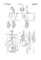
FIG. 1 illustrates a block diagram of the video controller of the present invention;
FIG. 2 illustrates a memory map showing available locations for the address space used for memory-mapped registers; and
FIG. 3 illustrates a block diagram of the decode logic used in the video controller for memory-mapping register addresses.
DETAILED DESCRIPTION OF THE INVENTION
The preferred embodiment of the present invention and its advantages are best understood by referring to FIGS. 1-3 of the drawings, like numerals being used for like and corresponding parts of the various drawings.
FIG. 1 illustrates a block diagram of the video controller 10 of the present invention. The video controller 10 is coupled to the processor over the bus 12. The video controller receives address bits and control signals from the processor over the bus 12. The number of address bits and control signals is dependent upon the processor and bus types. For an ISA bus, there are twenty-four address bits (A23 . . . A0) and for an EISA bus type, there are thirty-two address bits (A31 . . . A0).
The video controller 10 comprises a controller 14, a frame buffer 16 and a digital-to-analog converter (DAC) 18. The controller 14 is responsible for controlling the transfer of video information from the bus 12 to the frame buffer 16. The operation of the controller 14 is controlled in part through values stored in registers 20. In the present invention, both memory-mapped registers 22 and I/O-mapped registers 24 are used.
The use of registers to control the operation of the video controller is well-known in the art; a listing of memory-mapped registers used in the preferred embodiment is provided hereinbelow in connection with Table I.
              TABLE I                                                     
______________________________________                                    
MEMORY MAPPED REGISTERS                                                   
MEM                                                                       
ADDR   IO ADDR   REGISTER         SIZE  R/W                               
______________________________________                                    
101    385/3D5   CRTC data        8-bit R/W                               
Graphics configuration and control registers.                             
108    3CE       Graphics Index   8-bit R/W                               
109    3CF       Graphics data    8-bit R/W                               
Configuration and status registers                                        
120    63C4/73C4 Active line counter                                      
                                  8-bit R                                 
121    63C5/73C5 Active line counter                                      
                                  8-bit R                                 
122    3BA3DA    Input status 1   8-bit R                                 
123    3CF.10    Configuration register 1                                 
                                  8-bit R/W                               
Datepath registers                                                        
130    3C5.02    Sequencer plane mask                                     
                                  8-bit R/W                               
134    3CF.08    Sequencer bit mask                                       
                                  8-bit R/W                               
138    3CF.45    Page register 0  8-bit R/W                               
139    3CF.46    Page register 1  8-bit R/W                               
13A    3CF.03    Graphics data rotate                                     
                                  8-bit R/W                               
13B    3CF.04    Graphics read plane select                               
                                  8-bit R/W                               
13C    63CA/     QVGA Control Register 1                                  
                                  8-bit R/W                               
       73CA                                                               
13D    63CB/     QVGA Control Register 3                                  
                                  8-bit R/W                               
       73CB                                                               
13E    3CF.5A    Data path control                                        
                                  8-bit R/W                               
140    3CF.43    Foregound color register                                 
                                  8-bit R/W                               
141    33C6/53C6 Background color register                                
                                  8-bit R/W                               
142    33C6/53C6 Broadcast pattern register                               
                                  8-bit W                                 
143    33C7/53C7 Raster Operation All                                     
                                  8-bit W                                 
148    33C5/53C5 Raster Operation 0                                       
                                  8-bit R/W                               
149    33C4/53C4 Raster Operation 1                                       
                                  8-bit R/W                               
14A    33C3/53C3 Raster Operation 2                                       
                                  8-bit R/W                               
14B    33C2/53C2 Raster Operation 3                                       
                                  8-bit R/W                               
Line.sub.-- drawing engine registers                                      
160    3CF.60    Line command register                                    
                                  8-bit R/W                               
161    3CF.61    Line pattern pointer                                     
                                  8-bit R/W                               
162    3CF.62    Pattern end pointer                                      
                                  8-bit R/W                               
163    3CF.63    Line sign code   8-bit R/W                               
164    83C0/93C0 Line pattern byte 0                                      
                                  8-bit R/W                               
165    83C193C1  Line pattern byte 1                                      
                                  8-bit R/W                               
166    83C2/93C2 Line pattern byte 2                                      
                                  8-bit R/W                               
167    83C3/93C3 Line pattern byte 3                                      
                                  8-bit R/W                               
168-169                                                                   
       3CF.64-65 Line pixel count 16-bit                                  
                                        R/W                               
16C-16D                                                                   
       3CF.66-67 Line error term. 16-bit                                  
                                        R/W                               
170-171                                                                   
       3CF.68-69 Line K1 constant 16-bit                                  
                                        R/W                               
174-175                                                                   
       3CF.6A-6B Line K2 constant 16-bit                                  
                                        R/W                               
178-179                                                                   
       63C0-     Line X0          16-bit                                  
                                        R/W                               
       1/73xx                                                             
17A-17B                                                                   
       63C2-     Line Y0          16-bit                                  
                                        R/W                               
       3/73xx                                                             
17C-17D                                                                   
       83CC-D/   Line X1          16-bit                                  
                                        R/W                               
       93xx                                                               
17E-17F                                                                   
       83CE-F/   Line Y1          16-bit                                  
                                        R/W                               
       93xx                                                               
BitBLT engine registers                                                   
1A0    33CA/     Pattern register 0                                       
                                  8-bit R/W                               
       53CA                                                               
1A1    33CB/     Pattern register 1                                       
                                  8-bit R/W                               
       53CB                                                               
1A2    33CC/     Pattern register 2                                       
                                  8-bit R/W                               
       53CC                                                               
1A3    33CD/     Pattern register 3                                       
                                  8-bit R/W                               
       53CD                                                               
1A4    (33CA)    Pattern register 4                                       
                                  8-bit R/W                               
1A5    (33CB)    Pattern register 5                                       
                                  8-bit R/W                               
1A6    (33CC)    Pattern register 6                                       
                                  8-bit R/W                               
1A7    (33CD)    Pattern register 7                                       
                                  8-bit R/W                               
1A8-1A9                                                                   
       23CA-     BitBLT Source pitch                                      
                                  16-bit                                  
                                        R/W                               
       B/43xx                                                             
1AA-   23CE-F/   BitBLT Destination pitch                                 
                                  16-bit                                  
                                        R/W                               
1AB    43xx                                                               
1AC-   23C4-5/   Bitmap height    16-bit                                  
                                        R/W                               
1AD    43Cx                                                               
1AE-   23C2-3/   Bitmap width     16-bit                                  
                                        R/W                               
1AF    43Cx                                                               
1B0    33CE/     Bitbit command 1 8-bit R/W                               
       53CE                                                               
1B1    33CF/     Bitbit command 2 8-bit R/W                               
       53CF                                                               
1B8-1B9                                                                   
       63C0-     Bitbit source X0 16-bit                                  
                                        R/W                               
       1/73Cx                                                             
1BA-   63C2-     Bitbit source Y0 16-bit                                  
                                        R/W                               
1BB    3/73Cx                                                             
1BC-   63CC-     Bitbit destination X1                                    
                                  16-bit                                  
                                        R/W                               
1BD    D/73Cx                                                             
1BE-   63CE/     Bithit destination Y1                                    
                                  16-bit                                  
                                        R/W                               
1BF    73CE                                                               
Miscellaneous registers                                                   
1F8    None      FLASH PROM Register                                      
                                  8-bit R/W                               
1FC-   None      ORION Resvd Ct1  32-bit                                  
                                        R/W                               
1FF              Register                                                 
______________________________________                                    
The frame buffer 16 stores the pixel information which will be output to the display via the DAC 18. The size of the frame buffer may vary depending upon the maximum resolution and number of colors supported by the video controller 10. Table II provides the supported video modes for an exemplary video controller; however, other video modes could be used without departing from the present invention.
Each pixel is represented in the frame buffer 16 by one or more bits. The number of bits depends upon the number of colors supported. In monochrome mode (black and white), a single bit may represent each pixel. For sixteen-color operation, four bits are needed to represent each pixel. For true color operation (16.7 million colors), twenty-four bits are needed to represent each pixel. The number of pixels is determined by the resolution. Hence, for a resolution of 1024×768, the number of pixels represented in the frame buffer 16 numbers 786,432. In sixteen-color mode, therefore, 393,216 bytes of information would be needed in the frame buffer 16 to store the pixel information. Other information concerning operation of the controller 14 may also be stored in the frame buffer.
              TABLE II                                                    
______________________________________                                    
VIDEO MODES                                                               
RESOLUTION    BITS PER PIXEL SUPPORTED                                    
______________________________________                                    
512 × 480                                                           
              16, 32                                                      
640 × 400                                                           
              16, 32                                                      
640 × 480                                                           
              4, 8, 16, 32                                                
800 × 600                                                           
              4, 8, 16                                                    
1024 × 768                                                          
              4, 8, 16                                                    
1280 × 1024                                                         
              4, 8                                                        
______________________________________                                    
As shown in FIG. 1, the controller 14 uses both memory-mapped registers 22 and I/O-mapped registers 24. In general, the memory-mapped registers are those registers which will be updated frequently by the processor during execution of the program. By using memory-mapped registers to store the most frequently changed video information, the speed of the computer system is greatly enhanced.
In the preferred embodiment, several options are provided for accessing the memory-mapped registers. In the first option, the memory-mapped registers may be assigned a 4K address space within the memory address space used for the frame buffer 16. While the number of registers shown in Table I do not require 4K bytes of memory, the 4K address space is reserved for future expansion. The addresses shown in Table I are offset from the address denoting the last 512 bytes of memory in the 4K register address space.
Preferably, the address space used for the frame buffer 16 is programmably located anywhere within the system memory extended ("high") address space, i.e., the memory space above 1M. Hence, for a ISA bus, the frame buffer address space may be located anywhere within the sixteen megabyte address space available. For an EISA bus system, the frame buffer 16 may be located anywhere within the four gigabyte address space. When the memory-mapped registers are mapped to an address space within the frame buffer address space, the register address space is set to the highest 4K block in the frame buffer address space as shown in FIG. 2.
The second option is to locate the memory-mapped register address space within conventional ("low") memory (the memory located below the one megabyte address boundary). There are a number of blocks of memory reserved between the 640K and one megabyte address boundaries for various systems in the computer. Preferably, the 4K buffer used for the memory-mapped register address space is located within the "option ROM" area in conventional memory. It is desirable that the memory-mapped registers not be mapped to the system ROM area (the address space reserved for the computer BIOS) or the video buffer area reserved for block switching to the frame buffer when a program cannot access the address space above one megabyte ("extended" memory).
The third option is to disable memory-mapping such that the memory-mapped registers can only be accessed through I/O-space. It should be noted that even when the registers are memory-mapped either to low or high memory, they can always be accessed through a corresponding I/O-space address.
In general, it is preferable to map the memory-mapped registers to the address space used for the frame buffer. In some cases, it may be necessary to map the memory-mapped register to low memory, in order to support programs which cannot access extended memory. Disabling the memory-mapped addressing of the register is provided for compatibility with the pre-existing programs.
In order to implement the present invention, a number of the registers 20 of controller 14 are used to define the address space and size of the frame buffer 16 and the location of the address space for the memory-mapped registers. The registers used in a specific implementation of the present invention are described below; however, it is understood that other register configurations may be used without departing from the invention.
Control Register2 provides two bits for address control. Bit 0 of Control Register2 is the "register memory-map control" bit. If this bit is set to "1", memory-mapping of the registers 22 is enabled. If this bit is set to "0", the memory-mapping of the registers is disabled. On power-up, bit 0 is set to "0". Bit 2 of Control Register2 is the "high-address memory-map control bit". If this bit is set to "1", the memory-mapped registers 22 are mapped "high",i.e., to the upper 4K address space of the frame buffer memory address space. If this bit is set to "0", then the memory-mapped registers 22 are mapped "low", i.e., to conventional memory. On power-up, this bit set to "0".
Control Register3 provides a bit for selecting the memory configuration mode and determining the location of the memory-mapped I/O registers, if enabled in high memory. Bit 0 of Control Register3 is the "memory mode select" bit. If this bit is set to "1", then the frame buffer 16 is in "2 Mbyte mode", wherein two megabytes of system address space in extended memory will be decoded for the frame buffer. The memory-mapped I/O registers (if enabled in high memory) will be at the last 512 bytes in the 2 Mbyte area. If the memory mode select bit is set to "0", then the frame buffer 16 is in "1 Mbyte mode", wherein only one megabyte of system address space is decoded in extended memory for the frame buffer. The memory-mapped I/O registers (if enabled in high memory) will be set to the last 512 bytes in the 1M area.
In order for the memory-mapped registers 22 to be mapped in the frame buffer address area as the last 512 bytes of the specified frame buffer (as determined by bit "0" of Control Register3), bit "2" and bit "0" of Control Register2 must both be set to "1" and the High Address Register (discussed hereinbelow) must contain a non-zero value. The High Address Register provides twelve bits (bits 11-0) which are compared to address bits 31-20 of the address on bus 12 to determine whether an address is located within the boundaries of the frame buffer 16. Hence, by setting bits 11-0 of the High Address Register to a desired value, the frame buffer may be located anywhere within the system memory address space above 1M. If the value in the High Address Register is not "0", the memory-mapped registers 22 may be mapped high.
A Memory-Map Base Register is provided for mapping the memory-mapped registers 22 to the address space below one megabyte. This register is decoded only when the high address memory-map control bit (bit 2 of Control Register2) is set to "0". The Memory-Map Base Register includes bits 6-0 which define a 4K block of system memory space in the low memory area where the memory-mapped I/O registers are to be located. The registers themselves are specifically located in the last 512 bytes of the 4K block. Exemplary offsets for the registers specified in Table I are based off the beginning of the 512 byte area (i.e., the 4K block address plus E00h).
When the memory-mapped registers are enabled for low memory, bits 6-0 of the Memory-Map Base Register are compared against address lines A18-A12. Address lines A31-A20 (EISA interface) or A23-A20 (ISA interface) must be set to "0" and address line A19 must be set to "1" for low-mapped registers to be decoded. It should be noted that there are other requirements for the memory between 640K and one megabyte in a typical IBM-compatible computer system and the memory-mapped base register should be set accordingly in order to prevent conflicts. Also, it should be noted that if the memory-mapped registers are mapped in the video buffer address space accesses to the 4K block where the registers are mapped will prevent frame buffer accesses to the video buffer within that range (see FIG. 2).
It should be further noted that the memory-mapped registers 22 may be mapped low even though the frame buffer 16 is mapped high using the High Address Register.
FIG. 3 illustrates a block diagram of the portion of the controller 14 used to decode addresses on the bus 12 to determine whether the address corresponds to a memory-mapped register 22. The decoder section 50 comprises memory-mapped register decode logic 52, frame buffer decode logic 54 and I/O-mapped register decode logic 56. Memory-mapped register decode logic 52 and frame buffer decode logic 54 are coupled to registers 20 (specifically Control Register2 and Control Register3, the High Address Register and the Memory-Map Base Register). The frame buffer decode logic 54 outputs a signal FB-- SEL which indicates whether an address is in the frame buffer's address space. The memory-mapped register 52 outputs a signal indicating which of the memory-mapped registers 22 is selected responsive to an address specifying one of the memory-mapped registers 22. The I/O-mapped register decode logic 56 outputs a signal I/O-- REG-- SEL specifying the address of a register responsive to an address in I/O-space.
The frame buffer decode logic 54 sets FB-- SEL to a "1" if the address on the bus 12 is set to an address within the address space of the frame buffer (i.e., bits 11-0 of the High Address Register=address bits 31-20) and the M/IO# bit is set to "1". If FB-- SEL is set to "1", the memory-mapped register decode logic determines whether the address within the frame buffer address space is in the 4K address space reserved for the memory-mapped registers 22. If so, the address of the selected register is output. Similarly, if the high address memory-map control bit (bit 2 of Control Register2) indicates that the memory-mapped registers are mapped low and if the SMEM-- READ or SMEM-- WRITE signal is low (indicating-a read/write to low memory), then the memory-mapped register decode logic 52 determines whether the address is within the 4K block of system space in the low memory area defined by the Memory-Map Base Register.
If M/IO# is set to "0", the memory-mapped register decode logic 52 and the frame buffer decode logic 54 are disabled, and the I/O-mapped register decode logic 56 determines whether the I/O-space address is within the area reserved for the video controller 10 and generates the address of a register 20 responsive thereto.
As can be seen in FIG. 3, the decode logic 50 takes advantage of the frame buffer decode logic 54 which is normally available in a video controller 10 to determine whether an address is directed to the frame buffer 16. Hence, the only hardware addition is the memory-mapped register decode logic 52 and certain control bits and registers used to support the memory-mapping.
Although the preferred embodiment of the invention has been described in detail, it should be noted that various changes, substitutions and alterations could be made herein without departing from the spirit and scope of the invention as defined by the appended claims.

Claims (6)

What is claimed is:
1. A video controller comprising:
a video memory;
a first set of registers for storing control information;
a second set of registers for defining:
a first address space for said video memory in high memory;
a second address space for addressing said first set of registers in low memory addresses using memory mapped addresses;
whether memory mapping is used to address said first set of registers; and
whether memory mapping, if used, directs addresses to low memory or high memory; and
decode logic coupled to said first set of registers and said second set of registers, comprising:
circuitry to identify memory mapped addresses directed to said first set of registers; and
circuitry to identify I/O mapped addresses directed to said first set of registers.
2. The video controller of claim 1 wherein said circuitry to identify memory mapped addresses includes circuitry to identify memory mapped addresses within a predetermined portion of said first address space.
3. The video controller of claim 2 wherein said circuitry to identify memory mapped addresses further includes circuitry for identifying one of said first set of registers in response to a memory mapped address within said predetermined portion of said first address space.
4. A method of storing display information in a video controller comprising the steps of:
transferring data to a video memory responsive to control information in a first set of registers;
defining in a second set of registers:
a first address space for said video memory in high memory;
a second address space for addressing said first set of registers in low memory addresses using memory mapped addresses;
whether memory mapping is used to address said first set .Of registers; and
whether memory mapping, if used, directs addresses to low memory or high memory; and
responsive to said second set of registers:
identifying memory mapped addresses directed to said first set of registers and
identifying I/O mapped addresses directed to said first set of registers.
5. The method of claim 4 wherein said step of identifying memory mapped addresses includes the step of identifying memory mapped addresses within a predetermined portion of said first address space.
6. The method of claim 5 wherein said step of identifying memory mapped addresses further includes the step of identifying one of said first set of registers in response to a memory mapped address within said predetermined portion of said first address space.
US08/361,886 1993-05-14 1994-12-22 Memory mapped video control registers Expired - Lifetime US5506953A (en)

Priority Applications (2)

Application Number Priority Date Filing Date Title
US08/361,886 US5506953A (en) 1993-05-14 1994-12-22 Memory mapped video control registers
US08/560,892 US5617529A (en) 1993-05-14 1995-11-20 Memory-mapped video control registers

Applications Claiming Priority (2)

Application Number Priority Date Filing Date Title
US6229493A 1993-05-14 1993-05-14
US08/361,886 US5506953A (en) 1993-05-14 1994-12-22 Memory mapped video control registers

Related Parent Applications (1)

Application Number Title Priority Date Filing Date
US6229493A Continuation 1993-05-14 1993-05-14

Related Child Applications (1)

Application Number Title Priority Date Filing Date
US08/560,892 Continuation US5617529A (en) 1993-05-14 1995-11-20 Memory-mapped video control registers

Publications (1)

Publication Number Publication Date
US5506953A true US5506953A (en) 1996-04-09

Family

ID=22041541

Family Applications (2)

Application Number Title Priority Date Filing Date
US08/361,886 Expired - Lifetime US5506953A (en) 1993-05-14 1994-12-22 Memory mapped video control registers
US08/560,892 Expired - Lifetime US5617529A (en) 1993-05-14 1995-11-20 Memory-mapped video control registers

Family Applications After (1)

Application Number Title Priority Date Filing Date
US08/560,892 Expired - Lifetime US5617529A (en) 1993-05-14 1995-11-20 Memory-mapped video control registers

Country Status (1)

Country Link
US (2) US5506953A (en)

Cited By (10)

* Cited by examiner, † Cited by third party
Publication number Priority date Publication date Assignee Title
US5617529A (en) * 1993-05-14 1997-04-01 Compaq Computer Corporation Memory-mapped video control registers
US6604185B1 (en) 2000-07-20 2003-08-05 Silicon Graphics, Inc. Distribution of address-translation-purge requests to multiple processors
US6681293B1 (en) 2000-08-25 2004-01-20 Silicon Graphics, Inc. Method and cache-coherence system allowing purging of mid-level cache entries without purging lower-level cache entries
US6779072B1 (en) * 2000-07-20 2004-08-17 Silicon Graphics, Inc. Method and apparatus for accessing MMR registers distributed across a large asic
US6831924B1 (en) 2000-07-20 2004-12-14 Silicon Graphics, Inc. Variable mode bi-directional and uni-directional computer communication system
US6839856B1 (en) 2000-07-20 2005-01-04 Silicon Graphics, Inc. Method and circuit for reliable data capture in the presence of bus-master changeovers
US7009618B1 (en) * 2001-07-13 2006-03-07 Advanced Micro Devices, Inc. Integrated I/O Remapping mechanism
US7248635B1 (en) 2000-07-20 2007-07-24 Silicon Graphics, Inc. Method and apparatus for communicating computer data from one point to another over a communications medium
US7333516B1 (en) 2000-07-20 2008-02-19 Silicon Graphics, Inc. Interface for synchronous data transfer between domains clocked at different frequencies
US9024283B2 (en) 2010-06-22 2015-05-05 Micron Technology, Inc. Horizontally oriented and vertically stacked memory cells

Families Citing this family (11)

* Cited by examiner, † Cited by third party
Publication number Priority date Publication date Assignee Title
US6002411A (en) * 1994-11-16 1999-12-14 Interactive Silicon, Inc. Integrated video and memory controller with data processing and graphical processing capabilities
US5838334A (en) * 1994-11-16 1998-11-17 Dye; Thomas A. Memory and graphics controller which performs pointer-based display list video refresh operations
US6067098A (en) * 1994-11-16 2000-05-23 Interactive Silicon, Inc. Video/graphics controller which performs pointer-based display list video refresh operation
FR2749682B1 (en) * 1996-06-10 1998-07-10 Bull Sa CIRCUIT FOR TRANSFERRING DATA BETWEEN REMOTE MEMORIES AND COMPUTER COMPRISING SUCH A CIRCUIT
US5805166A (en) * 1996-08-23 1998-09-08 Intenational Business Machines Corp. Segmented status area for dynamically reporting status in a data processing system
US6336158B1 (en) * 1998-10-30 2002-01-01 Intel Corporation Memory based I/O decode arrangement, and system and method using the same
US6567091B2 (en) 2000-02-01 2003-05-20 Interactive Silicon, Inc. Video controller system with object display lists
US6725289B1 (en) * 2002-04-17 2004-04-20 Vmware, Inc. Transparent address remapping for high-speed I/O
US20090077273A1 (en) * 2007-09-18 2009-03-19 Barinder Singh Rai Control Data Transfer
CN102467453B (en) * 2010-11-17 2014-10-29 英业达股份有限公司 Method for setting internal memory address space
US9900548B2 (en) 2012-08-24 2018-02-20 Nxp Usa, Inc. Display control unit and method for generating a video signal

Citations (3)

* Cited by examiner, † Cited by third party
Publication number Priority date Publication date Assignee Title
US4908748A (en) * 1987-07-28 1990-03-13 Texas Instruments Incorporated Data processing device with parallel circular addressing hardware
US5201055A (en) * 1989-11-03 1993-04-06 Compaq Computer Corporation Multiprocessing system includes interprocessor encoding and decoding logic used for communication between two cards through reduced addressing lines
US5210850A (en) * 1990-06-15 1993-05-11 Compaq Computer Corporation Memory address space determination using programmable limit registers with single-ended comparators

Family Cites Families (1)

* Cited by examiner, † Cited by third party
Publication number Priority date Publication date Assignee Title
US5506953A (en) * 1993-05-14 1996-04-09 Compaq Computer Corporation Memory mapped video control registers

Patent Citations (3)

* Cited by examiner, † Cited by third party
Publication number Priority date Publication date Assignee Title
US4908748A (en) * 1987-07-28 1990-03-13 Texas Instruments Incorporated Data processing device with parallel circular addressing hardware
US5201055A (en) * 1989-11-03 1993-04-06 Compaq Computer Corporation Multiprocessing system includes interprocessor encoding and decoding logic used for communication between two cards through reduced addressing lines
US5210850A (en) * 1990-06-15 1993-05-11 Compaq Computer Corporation Memory address space determination using programmable limit registers with single-ended comparators

Cited By (12)

* Cited by examiner, † Cited by third party
Publication number Priority date Publication date Assignee Title
US5617529A (en) * 1993-05-14 1997-04-01 Compaq Computer Corporation Memory-mapped video control registers
US6604185B1 (en) 2000-07-20 2003-08-05 Silicon Graphics, Inc. Distribution of address-translation-purge requests to multiple processors
US6779072B1 (en) * 2000-07-20 2004-08-17 Silicon Graphics, Inc. Method and apparatus for accessing MMR registers distributed across a large asic
US6831924B1 (en) 2000-07-20 2004-12-14 Silicon Graphics, Inc. Variable mode bi-directional and uni-directional computer communication system
US6839856B1 (en) 2000-07-20 2005-01-04 Silicon Graphics, Inc. Method and circuit for reliable data capture in the presence of bus-master changeovers
US7248635B1 (en) 2000-07-20 2007-07-24 Silicon Graphics, Inc. Method and apparatus for communicating computer data from one point to another over a communications medium
US7333516B1 (en) 2000-07-20 2008-02-19 Silicon Graphics, Inc. Interface for synchronous data transfer between domains clocked at different frequencies
US6681293B1 (en) 2000-08-25 2004-01-20 Silicon Graphics, Inc. Method and cache-coherence system allowing purging of mid-level cache entries without purging lower-level cache entries
US7009618B1 (en) * 2001-07-13 2006-03-07 Advanced Micro Devices, Inc. Integrated I/O Remapping mechanism
US9024283B2 (en) 2010-06-22 2015-05-05 Micron Technology, Inc. Horizontally oriented and vertically stacked memory cells
US9349949B2 (en) 2010-06-22 2016-05-24 Micron Technology, Inc. Horizontally oriented and vertically stacked memory cells
US9627442B2 (en) 2010-06-22 2017-04-18 Micron Technology, Inc. Horizontally oriented and vertically stacked memory cells

Also Published As

Publication number Publication date
US5617529A (en) 1997-04-01

Similar Documents

Publication Publication Date Title
US5506953A (en) Memory mapped video control registers
EP0595880B1 (en) Memory management method
US5664139A (en) Method and a computer system for allocating and mapping frame buffers into expanded memory
US5404445A (en) External interface for a high performance graphics adapter allowing for graphics compatibility
US6411302B1 (en) Method and apparatus for addressing multiple frame buffers
EP0568078B1 (en) External interface for a high performance graphics adapter allowing for graphics compatibility
US7262776B1 (en) Incremental updating of animated displays using copy-on-write semantics
US5696924A (en) Memory access circuit with address translation performing auto increment of translated address on writes and return to translated address on reads
US6598136B1 (en) Data transfer with highly granular cacheability control between memory and a scratchpad area
JP2538029B2 (en) Computer display device
US6002411A (en) Integrated video and memory controller with data processing and graphical processing capabilities
US5644788A (en) Burst transfers using an ascending or descending only burst ordering
US5740464A (en) Architecture for providing input/output operations in a computer system
JP3854668B2 (en) A computer system for realizing a system management mode extended by a processor
US5721947A (en) Apparatus adapted to be joined between the system I/O bus and I/O devices which translates addresses furnished directly by an application program
US4103331A (en) Data processing display system
US6134641A (en) Method of and system for allowing a computer system to access cacheable memory in a non-cacheable manner
US5696923A (en) Graphics processor writing to shadow register at predetermined address simultaneously with writing to control register
US6741257B1 (en) Graphics engine command FIFO for programming multiple registers using a mapping index with register offsets
US5032981A (en) Method for increasing effective addressable data processing system memory space
JP2919774B2 (en) How to quickly point and copy shallow pixels in a deep framebuffer
US5659750A (en) Apparatus for context switching of input/output devices in responses to commands from unprivileged application programs
US6072508A (en) Method and apparatus for shortening display list instructions
EP1044411B1 (en) Computer with accelerated graphics port and multiple memory controllers and method of manufacture of said controllers
US5685011A (en) Apparatus for handling failures to provide a safe address translation in an improved input/output architecture for a computer system

Legal Events

Date Code Title Description
STCF Information on status: patent grant

Free format text: PATENTED CASE

CC Certificate of correction
FEPP Fee payment procedure

Free format text: PAYOR NUMBER ASSIGNED (ORIGINAL EVENT CODE: ASPN); ENTITY STATUS OF PATENT OWNER: LARGE ENTITY

FPAY Fee payment

Year of fee payment: 4

AS Assignment

Owner name: COMPAQ INFORMATION TECHNOLOGIES GROUP, L.P., TEXAS

Free format text: ASSIGNMENT OF ASSIGNORS INTEREST;ASSIGNOR:COMPAQ COMPUTER CORPORATION;REEL/FRAME:012418/0222

Effective date: 20010620

FPAY Fee payment

Year of fee payment: 8

AS Assignment

Owner name: HEWLETT-PACKARD DEVELOPMENT COMPANY, L.P., TEXAS

Free format text: CHANGE OF NAME;ASSIGNOR:COMPAQ INFORMATION TECHNOLOGIES GROUP, LP;REEL/FRAME:015000/0305

Effective date: 20021001

FPAY Fee payment

Year of fee payment: 12

REMI Maintenance fee reminder mailed
FEPP Fee payment procedure

Free format text: PAYOR NUMBER ASSIGNED (ORIGINAL EVENT CODE: ASPN); ENTITY STATUS OF PATENT OWNER: LARGE ENTITY

Free format text: PAYER NUMBER DE-ASSIGNED (ORIGINAL EVENT CODE: RMPN); ENTITY STATUS OF PATENT OWNER: LARGE ENTITY