US5506446A - Electronic package having improved wire bonding capability - Google Patents
Electronic package having improved wire bonding capability Download PDFInfo
- Publication number
- US5506446A US5506446A US08/450,292 US45029295A US5506446A US 5506446 A US5506446 A US 5506446A US 45029295 A US45029295 A US 45029295A US 5506446 A US5506446 A US 5506446A
- Authority
- US
- United States
- Prior art keywords
- electronic package
- base
- lead support
- lead
- electrically insulating
- Prior art date
- Legal status (The legal status is an assumption and is not a legal conclusion. Google has not performed a legal analysis and makes no representation as to the accuracy of the status listed.)
- Expired - Fee Related
Links
Images


Classifications
-
- H—ELECTRICITY
- H01—ELECTRIC ELEMENTS
- H01L—SEMICONDUCTOR DEVICES NOT COVERED BY CLASS H10
- H01L24/00—Arrangements for connecting or disconnecting semiconductor or solid-state bodies; Methods or apparatus related thereto
- H01L24/01—Means for bonding being attached to, or being formed on, the surface to be connected, e.g. chip-to-package, die-attach, "first-level" interconnects; Manufacturing methods related thereto
- H01L24/26—Layer connectors, e.g. plate connectors, solder or adhesive layers; Manufacturing methods related thereto
- H01L24/31—Structure, shape, material or disposition of the layer connectors after the connecting process
- H01L24/32—Structure, shape, material or disposition of the layer connectors after the connecting process of an individual layer connector
-
- H—ELECTRICITY
- H01—ELECTRIC ELEMENTS
- H01L—SEMICONDUCTOR DEVICES NOT COVERED BY CLASS H10
- H01L23/00—Details of semiconductor or other solid state devices
- H01L23/02—Containers; Seals
- H01L23/04—Containers; Seals characterised by the shape of the container or parts, e.g. caps, walls
- H01L23/053—Containers; Seals characterised by the shape of the container or parts, e.g. caps, walls the container being a hollow construction and having an insulating or insulated base as a mounting for the semiconductor body
- H01L23/057—Containers; Seals characterised by the shape of the container or parts, e.g. caps, walls the container being a hollow construction and having an insulating or insulated base as a mounting for the semiconductor body the leads being parallel to the base
-
- H—ELECTRICITY
- H01—ELECTRIC ELEMENTS
- H01L—SEMICONDUCTOR DEVICES NOT COVERED BY CLASS H10
- H01L23/00—Details of semiconductor or other solid state devices
- H01L23/48—Arrangements for conducting electric current to or from the solid state body in operation, e.g. leads, terminal arrangements ; Selection of materials therefor
- H01L23/488—Arrangements for conducting electric current to or from the solid state body in operation, e.g. leads, terminal arrangements ; Selection of materials therefor consisting of soldered or bonded constructions
- H01L23/498—Leads, i.e. metallisations or lead-frames on insulating substrates, e.g. chip carriers
- H01L23/49861—Lead-frames fixed on or encapsulated in insulating substrates
-
- H—ELECTRICITY
- H01—ELECTRIC ELEMENTS
- H01L—SEMICONDUCTOR DEVICES NOT COVERED BY CLASS H10
- H01L2224/00—Indexing scheme for arrangements for connecting or disconnecting semiconductor or solid-state bodies and methods related thereto as covered by H01L24/00
- H01L2224/01—Means for bonding being attached to, or being formed on, the surface to be connected, e.g. chip-to-package, die-attach, "first-level" interconnects; Manufacturing methods related thereto
- H01L2224/26—Layer connectors, e.g. plate connectors, solder or adhesive layers; Manufacturing methods related thereto
- H01L2224/2612—Auxiliary members for layer connectors, e.g. spacers
-
- H—ELECTRICITY
- H01—ELECTRIC ELEMENTS
- H01L—SEMICONDUCTOR DEVICES NOT COVERED BY CLASS H10
- H01L2224/00—Indexing scheme for arrangements for connecting or disconnecting semiconductor or solid-state bodies and methods related thereto as covered by H01L24/00
- H01L2224/01—Means for bonding being attached to, or being formed on, the surface to be connected, e.g. chip-to-package, die-attach, "first-level" interconnects; Manufacturing methods related thereto
- H01L2224/26—Layer connectors, e.g. plate connectors, solder or adhesive layers; Manufacturing methods related thereto
- H01L2224/31—Structure, shape, material or disposition of the layer connectors after the connecting process
- H01L2224/32—Structure, shape, material or disposition of the layer connectors after the connecting process of an individual layer connector
- H01L2224/3201—Structure
- H01L2224/32012—Structure relative to the bonding area, e.g. bond pad
- H01L2224/32013—Structure relative to the bonding area, e.g. bond pad the layer connector being larger than the bonding area, e.g. bond pad
-
- H—ELECTRICITY
- H01—ELECTRIC ELEMENTS
- H01L—SEMICONDUCTOR DEVICES NOT COVERED BY CLASS H10
- H01L2224/00—Indexing scheme for arrangements for connecting or disconnecting semiconductor or solid-state bodies and methods related thereto as covered by H01L24/00
- H01L2224/01—Means for bonding being attached to, or being formed on, the surface to be connected, e.g. chip-to-package, die-attach, "first-level" interconnects; Manufacturing methods related thereto
- H01L2224/42—Wire connectors; Manufacturing methods related thereto
- H01L2224/44—Structure, shape, material or disposition of the wire connectors prior to the connecting process
- H01L2224/45—Structure, shape, material or disposition of the wire connectors prior to the connecting process of an individual wire connector
- H01L2224/45001—Core members of the connector
- H01L2224/4501—Shape
- H01L2224/45012—Cross-sectional shape
- H01L2224/45015—Cross-sectional shape being circular
-
- H—ELECTRICITY
- H01—ELECTRIC ELEMENTS
- H01L—SEMICONDUCTOR DEVICES NOT COVERED BY CLASS H10
- H01L2224/00—Indexing scheme for arrangements for connecting or disconnecting semiconductor or solid-state bodies and methods related thereto as covered by H01L24/00
- H01L2224/01—Means for bonding being attached to, or being formed on, the surface to be connected, e.g. chip-to-package, die-attach, "first-level" interconnects; Manufacturing methods related thereto
- H01L2224/42—Wire connectors; Manufacturing methods related thereto
- H01L2224/44—Structure, shape, material or disposition of the wire connectors prior to the connecting process
- H01L2224/45—Structure, shape, material or disposition of the wire connectors prior to the connecting process of an individual wire connector
- H01L2224/45001—Core members of the connector
- H01L2224/45099—Material
- H01L2224/451—Material with a principal constituent of the material being a metal or a metalloid, e.g. boron (B), silicon (Si), germanium (Ge), arsenic (As), antimony (Sb), tellurium (Te) and polonium (Po), and alloys thereof
- H01L2224/45117—Material with a principal constituent of the material being a metal or a metalloid, e.g. boron (B), silicon (Si), germanium (Ge), arsenic (As), antimony (Sb), tellurium (Te) and polonium (Po), and alloys thereof the principal constituent melting at a temperature of greater than or equal to 400°C and less than 950°C
- H01L2224/45124—Aluminium (Al) as principal constituent
-
- H—ELECTRICITY
- H01—ELECTRIC ELEMENTS
- H01L—SEMICONDUCTOR DEVICES NOT COVERED BY CLASS H10
- H01L2224/00—Indexing scheme for arrangements for connecting or disconnecting semiconductor or solid-state bodies and methods related thereto as covered by H01L24/00
- H01L2224/01—Means for bonding being attached to, or being formed on, the surface to be connected, e.g. chip-to-package, die-attach, "first-level" interconnects; Manufacturing methods related thereto
- H01L2224/42—Wire connectors; Manufacturing methods related thereto
- H01L2224/44—Structure, shape, material or disposition of the wire connectors prior to the connecting process
- H01L2224/45—Structure, shape, material or disposition of the wire connectors prior to the connecting process of an individual wire connector
- H01L2224/45001—Core members of the connector
- H01L2224/45099—Material
- H01L2224/451—Material with a principal constituent of the material being a metal or a metalloid, e.g. boron (B), silicon (Si), germanium (Ge), arsenic (As), antimony (Sb), tellurium (Te) and polonium (Po), and alloys thereof
- H01L2224/45138—Material with a principal constituent of the material being a metal or a metalloid, e.g. boron (B), silicon (Si), germanium (Ge), arsenic (As), antimony (Sb), tellurium (Te) and polonium (Po), and alloys thereof the principal constituent melting at a temperature of greater than or equal to 950°C and less than 1550°C
- H01L2224/45144—Gold (Au) as principal constituent
-
- H—ELECTRICITY
- H01—ELECTRIC ELEMENTS
- H01L—SEMICONDUCTOR DEVICES NOT COVERED BY CLASS H10
- H01L2224/00—Indexing scheme for arrangements for connecting or disconnecting semiconductor or solid-state bodies and methods related thereto as covered by H01L24/00
- H01L2224/01—Means for bonding being attached to, or being formed on, the surface to be connected, e.g. chip-to-package, die-attach, "first-level" interconnects; Manufacturing methods related thereto
- H01L2224/42—Wire connectors; Manufacturing methods related thereto
- H01L2224/44—Structure, shape, material or disposition of the wire connectors prior to the connecting process
- H01L2224/45—Structure, shape, material or disposition of the wire connectors prior to the connecting process of an individual wire connector
- H01L2224/45001—Core members of the connector
- H01L2224/45099—Material
- H01L2224/451—Material with a principal constituent of the material being a metal or a metalloid, e.g. boron (B), silicon (Si), germanium (Ge), arsenic (As), antimony (Sb), tellurium (Te) and polonium (Po), and alloys thereof
- H01L2224/45138—Material with a principal constituent of the material being a metal or a metalloid, e.g. boron (B), silicon (Si), germanium (Ge), arsenic (As), antimony (Sb), tellurium (Te) and polonium (Po), and alloys thereof the principal constituent melting at a temperature of greater than or equal to 950°C and less than 1550°C
- H01L2224/45147—Copper (Cu) as principal constituent
-
- H—ELECTRICITY
- H01—ELECTRIC ELEMENTS
- H01L—SEMICONDUCTOR DEVICES NOT COVERED BY CLASS H10
- H01L2224/00—Indexing scheme for arrangements for connecting or disconnecting semiconductor or solid-state bodies and methods related thereto as covered by H01L24/00
- H01L2224/01—Means for bonding being attached to, or being formed on, the surface to be connected, e.g. chip-to-package, die-attach, "first-level" interconnects; Manufacturing methods related thereto
- H01L2224/42—Wire connectors; Manufacturing methods related thereto
- H01L2224/47—Structure, shape, material or disposition of the wire connectors after the connecting process
- H01L2224/48—Structure, shape, material or disposition of the wire connectors after the connecting process of an individual wire connector
- H01L2224/4805—Shape
- H01L2224/4809—Loop shape
- H01L2224/48091—Arched
-
- H—ELECTRICITY
- H01—ELECTRIC ELEMENTS
- H01L—SEMICONDUCTOR DEVICES NOT COVERED BY CLASS H10
- H01L2224/00—Indexing scheme for arrangements for connecting or disconnecting semiconductor or solid-state bodies and methods related thereto as covered by H01L24/00
- H01L2224/01—Means for bonding being attached to, or being formed on, the surface to be connected, e.g. chip-to-package, die-attach, "first-level" interconnects; Manufacturing methods related thereto
- H01L2224/42—Wire connectors; Manufacturing methods related thereto
- H01L2224/47—Structure, shape, material or disposition of the wire connectors after the connecting process
- H01L2224/48—Structure, shape, material or disposition of the wire connectors after the connecting process of an individual wire connector
- H01L2224/481—Disposition
- H01L2224/48151—Connecting between a semiconductor or solid-state body and an item not being a semiconductor or solid-state body, e.g. chip-to-substrate, chip-to-passive
- H01L2224/48221—Connecting between a semiconductor or solid-state body and an item not being a semiconductor or solid-state body, e.g. chip-to-substrate, chip-to-passive the body and the item being stacked
- H01L2224/48245—Connecting between a semiconductor or solid-state body and an item not being a semiconductor or solid-state body, e.g. chip-to-substrate, chip-to-passive the body and the item being stacked the item being metallic
- H01L2224/48247—Connecting between a semiconductor or solid-state body and an item not being a semiconductor or solid-state body, e.g. chip-to-substrate, chip-to-passive the body and the item being stacked the item being metallic connecting the wire to a bond pad of the item
-
- H—ELECTRICITY
- H01—ELECTRIC ELEMENTS
- H01L—SEMICONDUCTOR DEVICES NOT COVERED BY CLASS H10
- H01L2224/00—Indexing scheme for arrangements for connecting or disconnecting semiconductor or solid-state bodies and methods related thereto as covered by H01L24/00
- H01L2224/73—Means for bonding being of different types provided for in two or more of groups H01L2224/10, H01L2224/18, H01L2224/26, H01L2224/34, H01L2224/42, H01L2224/50, H01L2224/63, H01L2224/71
- H01L2224/732—Location after the connecting process
- H01L2224/73251—Location after the connecting process on different surfaces
- H01L2224/73265—Layer and wire connectors
-
- H—ELECTRICITY
- H01—ELECTRIC ELEMENTS
- H01L—SEMICONDUCTOR DEVICES NOT COVERED BY CLASS H10
- H01L2224/00—Indexing scheme for arrangements for connecting or disconnecting semiconductor or solid-state bodies and methods related thereto as covered by H01L24/00
- H01L2224/80—Methods for connecting semiconductor or other solid state bodies using means for bonding being attached to, or being formed on, the surface to be connected
- H01L2224/85—Methods for connecting semiconductor or other solid state bodies using means for bonding being attached to, or being formed on, the surface to be connected using a wire connector
- H01L2224/852—Applying energy for connecting
- H01L2224/85201—Compression bonding
- H01L2224/85205—Ultrasonic bonding
-
- H—ELECTRICITY
- H01—ELECTRIC ELEMENTS
- H01L—SEMICONDUCTOR DEVICES NOT COVERED BY CLASS H10
- H01L24/00—Arrangements for connecting or disconnecting semiconductor or solid-state bodies; Methods or apparatus related thereto
- H01L24/01—Means for bonding being attached to, or being formed on, the surface to be connected, e.g. chip-to-package, die-attach, "first-level" interconnects; Manufacturing methods related thereto
- H01L24/42—Wire connectors; Manufacturing methods related thereto
- H01L24/44—Structure, shape, material or disposition of the wire connectors prior to the connecting process
- H01L24/45—Structure, shape, material or disposition of the wire connectors prior to the connecting process of an individual wire connector
-
- H—ELECTRICITY
- H01—ELECTRIC ELEMENTS
- H01L—SEMICONDUCTOR DEVICES NOT COVERED BY CLASS H10
- H01L24/00—Arrangements for connecting or disconnecting semiconductor or solid-state bodies; Methods or apparatus related thereto
- H01L24/01—Means for bonding being attached to, or being formed on, the surface to be connected, e.g. chip-to-package, die-attach, "first-level" interconnects; Manufacturing methods related thereto
- H01L24/42—Wire connectors; Manufacturing methods related thereto
- H01L24/47—Structure, shape, material or disposition of the wire connectors after the connecting process
- H01L24/48—Structure, shape, material or disposition of the wire connectors after the connecting process of an individual wire connector
-
- H—ELECTRICITY
- H01—ELECTRIC ELEMENTS
- H01L—SEMICONDUCTOR DEVICES NOT COVERED BY CLASS H10
- H01L2924/00—Indexing scheme for arrangements or methods for connecting or disconnecting semiconductor or solid-state bodies as covered by H01L24/00
- H01L2924/0001—Technical content checked by a classifier
- H01L2924/00014—Technical content checked by a classifier the subject-matter covered by the group, the symbol of which is combined with the symbol of this group, being disclosed without further technical details
-
- H—ELECTRICITY
- H01—ELECTRIC ELEMENTS
- H01L—SEMICONDUCTOR DEVICES NOT COVERED BY CLASS H10
- H01L2924/00—Indexing scheme for arrangements or methods for connecting or disconnecting semiconductor or solid-state bodies as covered by H01L24/00
- H01L2924/01—Chemical elements
- H01L2924/01006—Carbon [C]
-
- H—ELECTRICITY
- H01—ELECTRIC ELEMENTS
- H01L—SEMICONDUCTOR DEVICES NOT COVERED BY CLASS H10
- H01L2924/00—Indexing scheme for arrangements or methods for connecting or disconnecting semiconductor or solid-state bodies as covered by H01L24/00
- H01L2924/01—Chemical elements
- H01L2924/01013—Aluminum [Al]
-
- H—ELECTRICITY
- H01—ELECTRIC ELEMENTS
- H01L—SEMICONDUCTOR DEVICES NOT COVERED BY CLASS H10
- H01L2924/00—Indexing scheme for arrangements or methods for connecting or disconnecting semiconductor or solid-state bodies as covered by H01L24/00
- H01L2924/01—Chemical elements
- H01L2924/01014—Silicon [Si]
-
- H—ELECTRICITY
- H01—ELECTRIC ELEMENTS
- H01L—SEMICONDUCTOR DEVICES NOT COVERED BY CLASS H10
- H01L2924/00—Indexing scheme for arrangements or methods for connecting or disconnecting semiconductor or solid-state bodies as covered by H01L24/00
- H01L2924/01—Chemical elements
- H01L2924/01028—Nickel [Ni]
-
- H—ELECTRICITY
- H01—ELECTRIC ELEMENTS
- H01L—SEMICONDUCTOR DEVICES NOT COVERED BY CLASS H10
- H01L2924/00—Indexing scheme for arrangements or methods for connecting or disconnecting semiconductor or solid-state bodies as covered by H01L24/00
- H01L2924/01—Chemical elements
- H01L2924/01029—Copper [Cu]
-
- H—ELECTRICITY
- H01—ELECTRIC ELEMENTS
- H01L—SEMICONDUCTOR DEVICES NOT COVERED BY CLASS H10
- H01L2924/00—Indexing scheme for arrangements or methods for connecting or disconnecting semiconductor or solid-state bodies as covered by H01L24/00
- H01L2924/01—Chemical elements
- H01L2924/01033—Arsenic [As]
-
- H—ELECTRICITY
- H01—ELECTRIC ELEMENTS
- H01L—SEMICONDUCTOR DEVICES NOT COVERED BY CLASS H10
- H01L2924/00—Indexing scheme for arrangements or methods for connecting or disconnecting semiconductor or solid-state bodies as covered by H01L24/00
- H01L2924/01—Chemical elements
- H01L2924/01046—Palladium [Pd]
-
- H—ELECTRICITY
- H01—ELECTRIC ELEMENTS
- H01L—SEMICONDUCTOR DEVICES NOT COVERED BY CLASS H10
- H01L2924/00—Indexing scheme for arrangements or methods for connecting or disconnecting semiconductor or solid-state bodies as covered by H01L24/00
- H01L2924/01—Chemical elements
- H01L2924/01047—Silver [Ag]
-
- H—ELECTRICITY
- H01—ELECTRIC ELEMENTS
- H01L—SEMICONDUCTOR DEVICES NOT COVERED BY CLASS H10
- H01L2924/00—Indexing scheme for arrangements or methods for connecting or disconnecting semiconductor or solid-state bodies as covered by H01L24/00
- H01L2924/01—Chemical elements
- H01L2924/01079—Gold [Au]
-
- H—ELECTRICITY
- H01—ELECTRIC ELEMENTS
- H01L—SEMICONDUCTOR DEVICES NOT COVERED BY CLASS H10
- H01L2924/00—Indexing scheme for arrangements or methods for connecting or disconnecting semiconductor or solid-state bodies as covered by H01L24/00
- H01L2924/01—Chemical elements
- H01L2924/01082—Lead [Pb]
-
- H—ELECTRICITY
- H01—ELECTRIC ELEMENTS
- H01L—SEMICONDUCTOR DEVICES NOT COVERED BY CLASS H10
- H01L2924/00—Indexing scheme for arrangements or methods for connecting or disconnecting semiconductor or solid-state bodies as covered by H01L24/00
- H01L2924/013—Alloys
- H01L2924/0132—Binary Alloys
- H01L2924/01327—Intermediate phases, i.e. intermetallics compounds
-
- H—ELECTRICITY
- H01—ELECTRIC ELEMENTS
- H01L—SEMICONDUCTOR DEVICES NOT COVERED BY CLASS H10
- H01L2924/00—Indexing scheme for arrangements or methods for connecting or disconnecting semiconductor or solid-state bodies as covered by H01L24/00
- H01L2924/095—Indexing scheme for arrangements or methods for connecting or disconnecting semiconductor or solid-state bodies as covered by H01L24/00 with a principal constituent of the material being a combination of two or more materials provided in the groups H01L2924/013 - H01L2924/0715
- H01L2924/097—Glass-ceramics, e.g. devitrified glass
- H01L2924/09701—Low temperature co-fired ceramic [LTCC]
-
- H—ELECTRICITY
- H01—ELECTRIC ELEMENTS
- H01L—SEMICONDUCTOR DEVICES NOT COVERED BY CLASS H10
- H01L2924/00—Indexing scheme for arrangements or methods for connecting or disconnecting semiconductor or solid-state bodies as covered by H01L24/00
- H01L2924/15—Details of package parts other than the semiconductor or other solid state devices to be connected
- H01L2924/151—Die mounting substrate
- H01L2924/1515—Shape
- H01L2924/15153—Shape the die mounting substrate comprising a recess for hosting the device
-
- H—ELECTRICITY
- H01—ELECTRIC ELEMENTS
- H01L—SEMICONDUCTOR DEVICES NOT COVERED BY CLASS H10
- H01L2924/00—Indexing scheme for arrangements or methods for connecting or disconnecting semiconductor or solid-state bodies as covered by H01L24/00
- H01L2924/15—Details of package parts other than the semiconductor or other solid state devices to be connected
- H01L2924/151—Die mounting substrate
- H01L2924/15165—Monolayer substrate
-
- H—ELECTRICITY
- H01—ELECTRIC ELEMENTS
- H01L—SEMICONDUCTOR DEVICES NOT COVERED BY CLASS H10
- H01L2924/00—Indexing scheme for arrangements or methods for connecting or disconnecting semiconductor or solid-state bodies as covered by H01L24/00
- H01L2924/15—Details of package parts other than the semiconductor or other solid state devices to be connected
- H01L2924/161—Cap
- H01L2924/1615—Shape
- H01L2924/16151—Cap comprising an aperture, e.g. for pressure control, encapsulation
-
- H—ELECTRICITY
- H01—ELECTRIC ELEMENTS
- H01L—SEMICONDUCTOR DEVICES NOT COVERED BY CLASS H10
- H01L2924/00—Indexing scheme for arrangements or methods for connecting or disconnecting semiconductor or solid-state bodies as covered by H01L24/00
- H01L2924/15—Details of package parts other than the semiconductor or other solid state devices to be connected
- H01L2924/161—Cap
- H01L2924/1615—Shape
- H01L2924/16152—Cap comprising a cavity for hosting the device, e.g. U-shaped cap
-
- H—ELECTRICITY
- H01—ELECTRIC ELEMENTS
- H01L—SEMICONDUCTOR DEVICES NOT COVERED BY CLASS H10
- H01L2924/00—Indexing scheme for arrangements or methods for connecting or disconnecting semiconductor or solid-state bodies as covered by H01L24/00
- H01L2924/15—Details of package parts other than the semiconductor or other solid state devices to be connected
- H01L2924/161—Cap
- H01L2924/1615—Shape
- H01L2924/16195—Flat cap [not enclosing an internal cavity]
-
- H—ELECTRICITY
- H01—ELECTRIC ELEMENTS
- H01L—SEMICONDUCTOR DEVICES NOT COVERED BY CLASS H10
- H01L2924/00—Indexing scheme for arrangements or methods for connecting or disconnecting semiconductor or solid-state bodies as covered by H01L24/00
- H01L2924/15—Details of package parts other than the semiconductor or other solid state devices to be connected
- H01L2924/181—Encapsulation
Definitions
- This invention relates to electronic packages to house one or more microelectronic devices such as silicon based semiconductor chips. More particularly, the inner lead tips of a leadframe are supported to prevent deflection during wire bonding.
- Electronic packages provide environmental protection for the delicate circuitry formed on a face of a semiconductor device.
- the packages also provide electrical interconnection between the circuitry and external circuits, typically through a leadframe or terminal pins.
- One electronic package has a metallic base and cover, the combination defining a cavity.
- a leadframe is disposed between the base and cover and adhesively bonded to both.
- a semiconductor device is supported on either a centrally positioned leadframe paddle or directly on the package base. Electrical interconnection between the device and the leadframe is by small diameter bond wires.
- This type of package is illustrated in U.S. Pat. Nos. 4,897,508 and 4,939,316, both by Mahulikar et al and both incorporated by reference in their entireties herein.
- the leadframe is a thin, typically on the order of 0.15 mm to 0.25 mm (0.006-0.010 inch), metallic strip formed from copper or an iron-nickel alloy.
- the metallic strip is patterned into a plurality of leads with inner lead portions approaching a central aperture and outer lead portions extending outward from the central aperture for electrical interconnection to external circuitry.
- the central aperture contains a paddle formed from the same metallic strip as the leadframe and supported by outward running tie bars.
- the paddle facilitates assembly of the package.
- a semiconductor device is mounted to the paddle and small diameter bond wires electrically interconnect the device to the leadframe.
- the leadframe assembly is not yet housed within the electronic package and the inner leads are supported by external fixturing to prevent deflection during wire bonding.
- leadframes do not include this centrally positioned paddle and the semiconductor device is bonded directly to the base of the electronic package.
- the inner lead portions are supported by a polymer adhesive.
- this polymer adhesive is cured, nonuniform adhesive height can develop leading to a loss of lead coplanarity. Excess polymer resin can bleed on to the inner lead tips making wire bonding difficult. After the polymer cures, and wire bonding is commenced, the heat and pressure of bonding can deform the adhesive, deflecting the inner leads. Inner lead deflection leads to a poor wire bond or a short circuit.
- a feature of the invention is a lead support extending from the package base to support the inner lead portions.
- the lead support is either mounted on the base or an integral protrusion of the base.
- the lead support can be formed from a rigid polymer, a ceramic or an insulated metal.
- An advantage of the base assembly of the invention is that the inner lead portions do not deflect during wire bonding.
- the base assembly is particularly suited for aluminum bond wires leading to increased wire bond density and increased current carrying capacity.
- Another advantage is that the package does not require a die attach paddle for effective wire bonding improving the dissipation of heat from the device through the base.
- an electronic package base assembly includes a substrate having a peripheral portion and a central portion.
- a lead support is adjacent the substrate and disposed between the peripheral portion and the central portion.
- an electronic package In a second embodiment of the invention, there is provided an electronic package.
- the package has a base with a peripheral portion and a central portion.
- the electronic package includes a window frame having first and second opposing sides.
- a leadframe is disposed between the base and the first side of the window frame with an intermediate portion of the leadframe bonded to both the first side of the window frame and to the peripheral portion of the base.
- a lead support is disposed between the base and an inner lead portion of the lead frame. This lead support has a height effective to maintain the inner and intermediate portions of the leadframe in substantial coplanarity.
- FIG. 1 shows in cross-sectional representation an electronic package as known from the prior art.
- FIG. 2 shows in cross-sectional representation a window frame metal package as known from the prior art.
- FIG. 3 shows in cross-sectional representation a window frame package in accordance with the present invention.
- FIG. 4 shows a polymeric lead support in accordance with an embodiment of the invention.
- FIG. 5 shows in cross-sectional representation a polymeric lead support in accordance with another embodiment of the invention.
- FIG. 6 shows in cross-sectional representation a ceramic lead support in accordance with an embodiment of the invention.
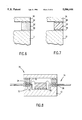
- FIG. 7 shows in cross-sectional representation an insulated metallic lead support in accordance with another embodiment of the invention.
- FIG. 8 shows in cross-sectional representation a metal electronic package having a unitary lead support in accordance with an embodiment of the invention.
- FIG. 9 shows in cross-sectional representation an electronic package having a unitary lead support in accordance with another embodiment of the invention.
- FIG. 10 shows in cross-sectional representation an embodiment of the invention in which the lead support extends beneath the semiconductor device.
- FIG. 11 shows in top isometric view the positioning of the lead support of the invention.
- FIG. 12 shows in top isometric view the lead support of FIG. 10 further including a plurality of circuit traces.
- FIG. 13 shows in cross-sectional representation the electronic packages of the invention sealed with an epoxy portion compounds.
- FIG. 1 An electronic package incorporating a die attach paddle, as known from the prior art, is illustrated in FIG. 1.
- the metal electronic package 10 has a base 12 and a cover 14. Disposed between the base 12 and the cover 14 is a leadframe 16.
- the leadframe 16 is typically formed from copper, a copper alloy or an iron/nickel alloy.
- the leadframe 16 has a plurality of leads disposed about a central aperture. The leads may be arbitrarily divided into three portions:
- the semiconductor device 20 is mounted on a centrally positioned die attach paddle 30 by a die attach 32.
- Conventional die attach 32 materials are electrically conductive polymers and low melting temperature solder.
- the semiconductor device 20 is first mounted to the die attach paddle 30.
- Wire bonds 22 then electrically interconnect the inner lead portions 18 of the leadframe 16 with input/output pads formed on the electrically active face of the semiconductor device 20.
- the leadframe is not yet incorporated into an electronic package and the inner lead portions 18 may be supported by an external fixture to prevent lead deflection during wire bonding.
- the assembly is then bonded to a package base 12 by a pad attach 34.
- pad attach 34 materials include electrically insulating, thermally conductive adhesives such as a thermosetting epoxy.
- the die attach paddle 30 is bonded to the package base 12 concurrent with the leadframe 16 being bonded to both the base 12 and cover 14.
- volatile compounds are given off. Some volatile compounds, such as chloride ions, become corrosive when combined with moisture. Accordingly, a vent hole 36 provides an egress for the volatiles following package assembly. After the adhesives are completely cured, a plug (not shown) seals the vent hole 36. Since some volatile components may remain in the package cavity, the wire bonds 22 are formed from gold or a gold alloy to reduce corrosion.
- a leadframe 16 is disposed between a base 12 and a window frame 42.
- the window frame 42 is an open rectangular structure having opposing first 44 and second 46 surfaces.
- the leadframe 16 is bonded by a polymer adhesive 26 to both the package base 12 and to the first surface 44 of the window frame 42.
- the polymer adhesive 26 also bonds a cover 14 to the second surface 46 of the window frame 42.
- a semiconductor device 20 is mounted directly to the base component 12 by die attach 32 or mounted on a die attach paddle and attached to the package base through a pad attach.
- Assembly of the window frame package 40 begins with bonding of the leadframe 16 to the package base 12 and to the first surface 44 of the window frame 42.
- the semiconductor device 20 is then bonded to the package base 12 by die attach 32.
- the inner lead portions 18 are electrically interconnected to the semiconductor device 20 by wire bonds 22.
- the cover 14 is bonded to the second surface 46 of the window frame 42.
- the cover 14 is attached after the adhesive cure is complete and fewer volatiles are trapped within the window frame package 40.
- the presence of corrosives within the package cavity is reduced and aluminum, copper or alloys thereof bond wires can be employed.
- copper or aluminum based bond wires rather than gold.
- aluminum and copper can carry a higher current per wire cross-sectional area than gold permitting more power to be delivered to the device.
- the inner lead portions of a lead frame are frequently coated with an aluminum layer to facilitate wire bonding.
- Gold wire bonds are susceptible to the formation of a brittle aluminum-gold intermetallic (commonly referred to as "purple plague").
- Aluminum bond wires bonded to an aluminum layer are immune to intermetallic formation.
- Gold bond wires are usually bonded thermosonically, forming a gold ball at the bond site.
- Aluminum bond wires can be bonded utilizing ultrasonics that form a narrow wedge at the bond site. The smaller pitch of the aluminum wedge increases the bond site density.
- a problem with the window frame package 40 is that the inner lead portion 18 is supported by the polymer adhesive 26. It is difficult to maintain lead coplanarity when the inner lead portions are supported by the adhesive. Additionally, if the adhesive volume is not accurately controlled, excess adhesive can bleed on to the inner lead portions making wire bonding difficult.
- the polymer adhesives such as thermosetting epoxies
- the polymer adhesives are not rigid, particularly at elevated wire bonding temperatures where the localized temperature can be in excess of 240° C.
- the inner lead portions 18 frequently deflect during wire bonding. The deflection weakens the wire bond strength and a deflected lead may contact an adjoining lead leading to an electrical short circuit.
- FIG. 3 shows in cross-sectional representation a window frame package 50 in accordance with the present invention.
- Many of the components of the window frame package 50 are similar to the components of the window frame package 40 of FIG. 2 and for like elements, the same reference numerals are utilized. Where related components perform a similar function, primed reference numerals are employed. Deflection of the inner lead portion 18 of the leadframe 16 during bonding of the wire bonds 22 is prevented by the lead support 52.
- the package base assembly 12' includes a substrate, corresponding to the base 12, having a peripheral portion 54 and a central portion 56.
- the peripheral portion 54 is adapted to receive a polymer adhesive for bonding to a leadframe.
- the central portion 56 is adapted to receive either a die attach or a pad attach. Adjacent the substrate and disposed between the peripheral portion 54 and the central portion 56 is the lead support 52.
- the substrate is formed from any suitable material which provides sufficient mechanical and environmental support to protect the fragile semiconductor device.
- Suitable substrate materials include metals, polymers and ceramics as well as composites and compounds incorporating these materials.
- Metals such as copper, aluminum and alloys thereof are particularly preferred.
- the high thermal conductivity of these metals is very effective in dissipating heat generated by the device.
- the lead support 52 has a height about equal to the thickness of the polymer adhesive 26 after the leadframe 16 is bonded to maintain the inner lead portion 18 and the intermediate portion 24 of the leadframe 16 in substantial coplanarity after the polymer adhesive is cured.
- the height of the lead support 52 is from about 0.1 mm to about 0.5 mm (0.004-0.020 inch).
- the lead support 52 is formed from any rigid material which will not deflect under the temperatures and pressures conventionally encountered during wire bonding.
- the material selected for the lead support has sufficient rigidity to resist deflecting more than about 0.075 mm (0.003 inch) during wire bonding. Preferably, the deflection is less than about 0.025 mm (0.001 inch). To achieve these objectives, the yield strength of the lead support 52 is in excess of about 130 MPa (20,000 psi) and preferably from about 130 MPa to about 552 MPa (80,000 psi).
- the lead support is formed from an electrically insulating material such as a polymer or ceramic.
- electrically insulating material such as a polymer or ceramic.
- metallic materials such as metals, metal alloys or metal compounds are useful when electrically isolated as described below.
- FIGS. 4 through 7 illustrate various embodiments of the lead support 52.
- the lead support 52 is formed from a rigid polymer adhesive such as a polyimide, a polyetheretherketone (“PEEK”) or a polyethersulfone.
- the rigid polymer adhesive bonds the inner lead ends 18 to the package base 12 for increased rigidity.
- the lead support 52 is a rigid polymer such as polyethersulfone or polyetheretherketone bonded to both the inner leads 18 and the package base 12 by a polymer adhesive 58.
- a suitable polymer adhesive for bonding the lead support to a metallic base 12 and metallic inner lead portion 18 is a thermosetting epoxy such as "ABLESTIK 550" (Ablestik Laboratories, Gardenia, Calif.).
- the polymer adhesive 58 is much thinner than adhesives used to bond a leadframe to a package base so the problem of loss of lead coplanarity and polymer resin bleed out is minimized.
- the lead support 52 is a ceramic such as aluminum oxide, silicon carbide or aluminum nitride.
- An electrically insulating, thermally conductive material such as aluminum nitride is preferred.
- the ceramic lead support 52 is bonded to the inner lead portion 18 and package base 12 by any suitable means such as a braze compound 60 or a polymer adhesive 58.
- a braze compound 60 When a braze compound 60 is utilized, the ceramic lead support 52 may be metallized and then brazed with a conventional braze such as a silver/copper alloy or a reactive metal braze such as a silver/copper/titanium alloy may be utilized for direct bonding to the ceramic.
- a suitable polymer adhesive 58 may also be utilized.
- the lead support 52 may be metallic which improves the conduction of heat from the inner leads 18 to the package base 12. To prevent an electrical short circuit, the lead support 52 is electrically isolated from the inner lead portion 18, and optionally from the package base 12 as well. Electrical isolation is provided by a polymer adhesive 58 or by applying a dielectric layer to at least one surface of the metallic lead support 52 disposed between the base 12 and inner lead portion 18. When the metallic lead support 52 is aluminum or an aluminum alloy, the surfaces of the lead support can be anodized to provide electrical isolation.
- the lead support can be unitary with the substrate 12 as illustrated in FIG. 8.
- a groove 72 is formed around the perimeter of the base 12 by a suitable process such as milling. The depth of the groove 72 is that effective to receive the polymer adhesive 26. The groove 72 should have a depth such that when the polymer 26 bonds the base 12 to the leadframe 16, substantial coplanarity is maintained between the inner lead portion 18 and the intermediate portion 24.
- a dielectric layer 74 is disposed between the leadframe support 52 and inner lead portion 18.
- the dielectric layer 74 may be a coating, such as a polymer layer or integral with the base material 12. When the base is aluminum or an aluminum alloy, anodized aluminum is an effective dielectric layer.
- the depth of the channel 72 is adjusted to compensate for the thickness of the dielectric layer 74 to provide substantial coplanarity.
- FIG. 9 illustrates an electronic package 80 in which a peripheral channel 72 is formed around the base 12 by coining a groove 82 into an outermost surface 84 of the base 12.
- a lead support 52 is formed protruding from the opposing surface 86 of the base 12.
- the height of the protruding lead support 52 is that effective to maintain substantial coplanarity between the inner lead portion 18 and the intermediate lead portion 24 when the polymer adhesive 26 bonds the leadframe 16 to the base 12.
- a dielectric layer is preferably disposed between the inner lead 18 and lead support 52 to prevent an electrical short circuit.
- a rigid dielectric frame 90 overlies the central portion of the substrate 12 of an electronic package 100.
- the peripheral edge 91 of the rigid dielectric frame 90 is adjacent the peripheral portion of the substrate underlying the inner lead portions 18.
- the rigid dielectric layer 90 may be any non-conductive substrate and extends beneath the semiconductor device 20 and the inner lead end portions 18 of the leadframe 16.
- the rigid dielectric layer is an electrically conductive material having an electrically insulating material adjacent at least those surfaces contacting the inner lead portions 18.
- the thickness of the rigid dielectric 90 is that effective to maintain substantial coplanarity between the inner lead ends 18 and the intermediate portion 24 of the leadframe 16 when polymer adhesive 26 is cured.
- the rigid dielectric layer 90 may be any suitable material, including a metal coated with an insulating layer, the preferred materials are high thermal conductivity ceramics having a coefficient of thermal expansion approximately matching that of the semiconductor device 20. Suitable material include alumina (aluminum oxide), aluminum nitride, aluminum carbide, diamond, diamond-like (amorphous carbon) materials, silicon carbide, silicon nitride, beryllia and low temperature cofired substrates such as glass/ceramics. The high thermal conductivity of aluminum nitride makes that material particularly preferred.
- the rigid dielectric layer is bonded to the base 12 by attach 92 which could be a polymer, sealing glass, or if the rigid dielectric layer 90 is metallized, a solder or braze.
- FIG. 12 shows in top isometric view an alternative embodiment for the rigid dielectric layer 90.
- a plurality of circuit traces 94 are formed on a surface of the rigid dielectric layer 90 in accordance with any known method.
- a palladium/nickel alloy could be applied in a desired pattern by screen printing and copper deposited on that metallization by electrolytic or electroless means.
- the circuit traces 94 have a outside termination end 96 for electrical interconnection to the inner lead portions of a leadframe. Electrical interconnection can be by soldering, a conductive adhesive or wire bonding.
- the inside termination end 98 of the circuit traces 94 approach a central portion 100 of the rigid dielectric layer 100.
- the central portion 90 may be metallized to facilitate bonding of the semiconductor device.
- the inside termination ends 98 of the circuit traces 94 are then electrically interconnected to the semiconductor device such as by wire bonding or thin strips of copper foil as utilized in tape automated bonding.
- window frame package is illustrated with a cover 14, it is within the scope of the invention to fill the cavity defined by the base 12 and the window frame of any of the package assemblies with a potting compound such as an epoxy.
- This "lid free" package 110 is illustrated in cross sectional representation in FIG. 13.
- the potting compound 112 removes the requirement of a separate cover component resulting in the advantage of a reduced overall package thickness.
Abstract
Description
Claims (34)
Priority Applications (1)
| Application Number | Priority Date | Filing Date | Title |
|---|---|---|---|
| US08/450,292 US5506446A (en) | 1994-04-14 | 1995-05-25 | Electronic package having improved wire bonding capability |
Applications Claiming Priority (2)
| Application Number | Priority Date | Filing Date | Title |
|---|---|---|---|
| US22775494A | 1994-04-14 | 1994-04-14 | |
| US08/450,292 US5506446A (en) | 1994-04-14 | 1995-05-25 | Electronic package having improved wire bonding capability |
Related Parent Applications (1)
| Application Number | Title | Priority Date | Filing Date |
|---|---|---|---|
| US22775494A Continuation | 1994-04-14 | 1994-04-14 |
Publications (1)
| Publication Number | Publication Date |
|---|---|
| US5506446A true US5506446A (en) | 1996-04-09 |
Family
ID=22854324
Family Applications (1)
| Application Number | Title | Priority Date | Filing Date |
|---|---|---|---|
| US08/450,292 Expired - Fee Related US5506446A (en) | 1994-04-14 | 1995-05-25 | Electronic package having improved wire bonding capability |
Country Status (4)
| Country | Link |
|---|---|
| US (1) | US5506446A (en) |
| AU (1) | AU2231795A (en) |
| TW (1) | TW338183B (en) |
| WO (1) | WO1995028740A1 (en) |
Cited By (39)
| Publication number | Priority date | Publication date | Assignee | Title |
|---|---|---|---|---|
| US5729050A (en) * | 1996-03-11 | 1998-03-17 | Lg Semicon Co., Ltd. | Semiconductor package substrate and ball grid array (BGA) semiconductor package using same |
| US5840427A (en) * | 1996-05-21 | 1998-11-24 | Teledyne Industries Incorporated | Method for making corrosion resistant electrical components |
| US5952719A (en) * | 1995-07-14 | 1999-09-14 | Advanced Interconnect Technologies, Inc. | Metal ball grid electronic package having improved solder joint |
| EP0951062A2 (en) * | 1998-04-18 | 1999-10-20 | TDK Corporation | Electronic part and manufacturing method therefor |
| US6001481A (en) * | 1995-03-08 | 1999-12-14 | Southwest Research Institute | Porous anodized aluminum surfaces sealed with diamond-like carbon coatings |
| US6042896A (en) * | 1995-03-08 | 2000-03-28 | Southwest Research Institute | Preventing radioactive contamination of porous surfaces |
| US6198163B1 (en) * | 1999-10-18 | 2001-03-06 | Amkor Technology, Inc. | Thin leadframe-type semiconductor package having heat sink with recess and exposed surface |
| US6248611B1 (en) | 1997-08-14 | 2001-06-19 | Micron Technology, Inc. | LOC semiconductor assembled with room temperature adhesive |
| US6396130B1 (en) | 2001-09-14 | 2002-05-28 | Amkor Technology, Inc. | Semiconductor package having multiple dies with independently biased back surfaces |
| US6410144B2 (en) | 1995-03-08 | 2002-06-25 | Southwest Research Institute | Lubricious diamond-like carbon coatings |
| US6479889B1 (en) * | 1998-09-04 | 2002-11-12 | Sony Corporation | Semiconductor device package, and fabrication method thereof |
| US6531341B1 (en) * | 2000-05-16 | 2003-03-11 | Sandia Corporation | Method of fabricating a microelectronic device package with an integral window |
| US6573124B1 (en) | 1999-05-03 | 2003-06-03 | Hughes Electronics Corp. | Preparation of passivated chip-on-board electronic devices |
| US20040173371A1 (en) * | 2001-09-14 | 2004-09-09 | Daisuke Fukushima | Surface mounting package |
| US20050285307A1 (en) * | 2004-06-24 | 2005-12-29 | Siemens Vdo Automotive Corporation | Alternate vent hole sealing method |
| WO2006113932A2 (en) * | 2005-04-20 | 2006-10-26 | International Rectifier Corporation | Chip-scale package |
| US20090102044A1 (en) * | 2007-10-23 | 2009-04-23 | Infineon Technologies Ag | Device including a housing for a semiconductor chip |
| US20090108421A1 (en) * | 2007-10-26 | 2009-04-30 | Infineon Technologies Ag | Apparatus and method configured to lower thermal stresses |
| US20090224380A1 (en) * | 2008-03-04 | 2009-09-10 | Powertech Technology Inc. | Leadframe and semiconductor package having downset baffle paddles |
| US20090289099A1 (en) * | 2004-04-01 | 2009-11-26 | Shinsuke Suzuki | Wire bonding method |
| US20110031865A1 (en) * | 2009-01-12 | 2011-02-10 | Hussell Christopher P | Light emitting device packages with improved heat transfer |
| USRE42319E1 (en) * | 1998-06-08 | 2011-05-03 | Mersen France Sb Sas | Circuit protection device |
| US20110180827A1 (en) * | 2009-06-05 | 2011-07-28 | Hussell Christopher P | Solid state lighting device |
| US8188592B2 (en) | 2007-10-26 | 2012-05-29 | Infineon Technologies Ag | Apparatus and method configured to lower thermal stresses |
| US20120292655A1 (en) * | 2011-05-18 | 2012-11-22 | Taiwan Semiconductor Manufacturing Company, Ltd. | Light emitting diode carrier |
| US20120319259A1 (en) * | 2011-06-16 | 2012-12-20 | Samsung Electro-Mechanics Co., Ltd. | Power module package and method for fabricating the same |
| USD679842S1 (en) | 2011-01-03 | 2013-04-09 | Cree, Inc. | High brightness LED package |
| US8610140B2 (en) | 2010-12-15 | 2013-12-17 | Cree, Inc. | Light emitting diode (LED) packages, systems, devices and related methods |
| US8648359B2 (en) | 2010-06-28 | 2014-02-11 | Cree, Inc. | Light emitting devices and methods |
| US8686445B1 (en) | 2009-06-05 | 2014-04-01 | Cree, Inc. | Solid state lighting devices and methods |
| USD708156S1 (en) | 2010-07-16 | 2014-07-01 | Cree, Inc. | Package for light emitting diode (LED) lighting |
| US8860043B2 (en) | 2009-06-05 | 2014-10-14 | Cree, Inc. | Light emitting device packages, systems and methods |
| US8878217B2 (en) | 2010-06-28 | 2014-11-04 | Cree, Inc. | LED package with efficient, isolated thermal path |
| US9111778B2 (en) | 2009-06-05 | 2015-08-18 | Cree, Inc. | Light emitting diode (LED) devices, systems, and methods |
| US9859471B2 (en) | 2011-01-31 | 2018-01-02 | Cree, Inc. | High brightness light emitting diode (LED) packages, systems and methods with improved resin filling and high adhesion |
| US20180261535A1 (en) * | 2014-12-15 | 2018-09-13 | Bridge Semiconductor Corp. | Method of making wiring board with dual routing circuitries integrated with leadframe |
| US20190355648A1 (en) * | 2018-05-18 | 2019-11-21 | Integra Technologies, Inc. | Semiconductor power device including ring frame for thermal impedance reduction |
| CN112614900A (en) * | 2020-11-27 | 2021-04-06 | 中国电子科技集团公司第十三研究所 | Light guide switch packaging structure |
| US11101408B2 (en) | 2011-02-07 | 2021-08-24 | Creeled, Inc. | Components and methods for light emitting diode (LED) lighting |
Citations (25)
| Publication number | Priority date | Publication date | Assignee | Title |
|---|---|---|---|---|
| US4105861A (en) * | 1975-09-29 | 1978-08-08 | Semi-Alloys, Inc. | Hermetically sealed container for semiconductor and other electronic devices |
| US4594770A (en) * | 1982-07-15 | 1986-06-17 | Olin Corporation | Method of making semiconductor casing |
| US4629824A (en) * | 1984-12-24 | 1986-12-16 | Gte Products Corporation | IC package sealing technique |
| US4721994A (en) * | 1985-06-25 | 1988-01-26 | Toray Silicone Co., Ltd. | Lead frame for semiconductor devices |
| US4784972A (en) * | 1984-08-18 | 1988-11-15 | Matsushita Electric Industrial Co. Ltd. | Method of joining beam leads with projections to device electrodes |
| US4796078A (en) * | 1987-06-15 | 1989-01-03 | International Business Machines Corporation | Peripheral/area wire bonding technique |
| US4827376A (en) * | 1987-10-05 | 1989-05-02 | Olin Corporation | Heat dissipating interconnect tape for use in tape automated bonding |
| US4849857A (en) * | 1987-10-05 | 1989-07-18 | Olin Corporation | Heat dissipating interconnect tape for use in tape automated bonding |
| US4888449A (en) * | 1988-01-04 | 1989-12-19 | Olin Corporation | Semiconductor package |
| US4897508A (en) * | 1988-02-10 | 1990-01-30 | Olin Corporation | Metal electronic package |
| US4939316A (en) * | 1988-10-05 | 1990-07-03 | Olin Corporation | Aluminum alloy semiconductor packages |
| US5008776A (en) * | 1990-06-06 | 1991-04-16 | Sgs-Thomson Microelectronics, Inc. | Zero power IC module |
| US5013871A (en) * | 1988-02-10 | 1991-05-07 | Olin Corporation | Kit for the assembly of a metal electronic package |
| US5025114A (en) * | 1989-10-30 | 1991-06-18 | Olin Corporation | Multi-layer lead frames for integrated circuit packages |
| US5034591A (en) * | 1988-03-22 | 1991-07-23 | Amdahl Corporation | Tape automated bonding leads having a stiffener and a method of bonding with same |
| US5073521A (en) * | 1989-11-15 | 1991-12-17 | Olin Corporation | Method for housing a tape-bonded electronic device and the package employed |
| US5086337A (en) * | 1987-01-19 | 1992-02-04 | Hitachi, Ltd. | Connecting structure of electronic part and electronic device using the structure |
| US5132773A (en) * | 1991-02-06 | 1992-07-21 | Olin Corporation | Carrier ring having first and second ring means with bonded surfaces |
| US5173766A (en) * | 1990-06-25 | 1992-12-22 | Lsi Logic Corporation | Semiconductor device package and method of making such a package |
| US5214307A (en) * | 1991-07-08 | 1993-05-25 | Micron Technology, Inc. | Lead frame for semiconductor devices having improved adhesive bond line control |
| JPH05136311A (en) * | 1991-11-14 | 1993-06-01 | Ngk Spark Plug Co Ltd | Package for integrated circuit |
| US5220195A (en) * | 1991-12-19 | 1993-06-15 | Motorola, Inc. | Semiconductor device having a multilayer leadframe with full power and ground planes |
| US5239131A (en) * | 1992-07-13 | 1993-08-24 | Olin Corporation | Electronic package having controlled epoxy flow |
| US5250839A (en) * | 1990-09-26 | 1993-10-05 | Dai Nippon Printing Co., Ltd. | Multi-layer leadframes, electrically conductive plates used therefor and production of such conductive plates |
| US5250842A (en) * | 1990-09-07 | 1993-10-05 | Nec Corporation | Semiconductor devices using tab tape |
-
1995
- 1995-03-30 AU AU22317/95A patent/AU2231795A/en not_active Abandoned
- 1995-03-30 WO PCT/US1995/003879 patent/WO1995028740A1/en active Application Filing
- 1995-04-13 TW TW084103598A patent/TW338183B/en active
- 1995-05-25 US US08/450,292 patent/US5506446A/en not_active Expired - Fee Related
Patent Citations (25)
| Publication number | Priority date | Publication date | Assignee | Title |
|---|---|---|---|---|
| US4105861A (en) * | 1975-09-29 | 1978-08-08 | Semi-Alloys, Inc. | Hermetically sealed container for semiconductor and other electronic devices |
| US4594770A (en) * | 1982-07-15 | 1986-06-17 | Olin Corporation | Method of making semiconductor casing |
| US4784972A (en) * | 1984-08-18 | 1988-11-15 | Matsushita Electric Industrial Co. Ltd. | Method of joining beam leads with projections to device electrodes |
| US4629824A (en) * | 1984-12-24 | 1986-12-16 | Gte Products Corporation | IC package sealing technique |
| US4721994A (en) * | 1985-06-25 | 1988-01-26 | Toray Silicone Co., Ltd. | Lead frame for semiconductor devices |
| US5086337A (en) * | 1987-01-19 | 1992-02-04 | Hitachi, Ltd. | Connecting structure of electronic part and electronic device using the structure |
| US4796078A (en) * | 1987-06-15 | 1989-01-03 | International Business Machines Corporation | Peripheral/area wire bonding technique |
| US4827376A (en) * | 1987-10-05 | 1989-05-02 | Olin Corporation | Heat dissipating interconnect tape for use in tape automated bonding |
| US4849857A (en) * | 1987-10-05 | 1989-07-18 | Olin Corporation | Heat dissipating interconnect tape for use in tape automated bonding |
| US4888449A (en) * | 1988-01-04 | 1989-12-19 | Olin Corporation | Semiconductor package |
| US5013871A (en) * | 1988-02-10 | 1991-05-07 | Olin Corporation | Kit for the assembly of a metal electronic package |
| US4897508A (en) * | 1988-02-10 | 1990-01-30 | Olin Corporation | Metal electronic package |
| US5034591A (en) * | 1988-03-22 | 1991-07-23 | Amdahl Corporation | Tape automated bonding leads having a stiffener and a method of bonding with same |
| US4939316A (en) * | 1988-10-05 | 1990-07-03 | Olin Corporation | Aluminum alloy semiconductor packages |
| US5025114A (en) * | 1989-10-30 | 1991-06-18 | Olin Corporation | Multi-layer lead frames for integrated circuit packages |
| US5073521A (en) * | 1989-11-15 | 1991-12-17 | Olin Corporation | Method for housing a tape-bonded electronic device and the package employed |
| US5008776A (en) * | 1990-06-06 | 1991-04-16 | Sgs-Thomson Microelectronics, Inc. | Zero power IC module |
| US5173766A (en) * | 1990-06-25 | 1992-12-22 | Lsi Logic Corporation | Semiconductor device package and method of making such a package |
| US5250842A (en) * | 1990-09-07 | 1993-10-05 | Nec Corporation | Semiconductor devices using tab tape |
| US5250839A (en) * | 1990-09-26 | 1993-10-05 | Dai Nippon Printing Co., Ltd. | Multi-layer leadframes, electrically conductive plates used therefor and production of such conductive plates |
| US5132773A (en) * | 1991-02-06 | 1992-07-21 | Olin Corporation | Carrier ring having first and second ring means with bonded surfaces |
| US5214307A (en) * | 1991-07-08 | 1993-05-25 | Micron Technology, Inc. | Lead frame for semiconductor devices having improved adhesive bond line control |
| JPH05136311A (en) * | 1991-11-14 | 1993-06-01 | Ngk Spark Plug Co Ltd | Package for integrated circuit |
| US5220195A (en) * | 1991-12-19 | 1993-06-15 | Motorola, Inc. | Semiconductor device having a multilayer leadframe with full power and ground planes |
| US5239131A (en) * | 1992-07-13 | 1993-08-24 | Olin Corporation | Electronic package having controlled epoxy flow |
Cited By (67)
| Publication number | Priority date | Publication date | Assignee | Title |
|---|---|---|---|---|
| US6410144B2 (en) | 1995-03-08 | 2002-06-25 | Southwest Research Institute | Lubricious diamond-like carbon coatings |
| US6001481A (en) * | 1995-03-08 | 1999-12-14 | Southwest Research Institute | Porous anodized aluminum surfaces sealed with diamond-like carbon coatings |
| US6042896A (en) * | 1995-03-08 | 2000-03-28 | Southwest Research Institute | Preventing radioactive contamination of porous surfaces |
| US6514565B2 (en) | 1995-03-08 | 2003-02-04 | Southwest Research Institute | Method for producing a lubricious amorphous carbon film |
| US5952719A (en) * | 1995-07-14 | 1999-09-14 | Advanced Interconnect Technologies, Inc. | Metal ball grid electronic package having improved solder joint |
| US5729050A (en) * | 1996-03-11 | 1998-03-17 | Lg Semicon Co., Ltd. | Semiconductor package substrate and ball grid array (BGA) semiconductor package using same |
| US5840427A (en) * | 1996-05-21 | 1998-11-24 | Teledyne Industries Incorporated | Method for making corrosion resistant electrical components |
| US6248611B1 (en) | 1997-08-14 | 2001-06-19 | Micron Technology, Inc. | LOC semiconductor assembled with room temperature adhesive |
| US6653721B2 (en) | 1997-08-14 | 2003-11-25 | Micron Technology, Inc. | LOC semiconductor assembled with room temperature adhesive |
| US6337511B1 (en) | 1997-08-14 | 2002-01-08 | Micron Technology, Inc. | LOC semiconductor assembled with room temperature adhesive |
| US6391680B2 (en) | 1997-08-14 | 2002-05-21 | Micron Technology, Inc. | LOC semiconductor assembled with room temperature adhesive |
| US20060022314A1 (en) * | 1997-08-14 | 2006-02-02 | Grigg Ford B | LOC semiconductor assembled with room temperature adhesive |
| US6316823B1 (en) * | 1997-08-14 | 2001-11-13 | Micron Technology, Inc. | LOC semiconductor assembled with room temperature adhesive |
| US6979888B2 (en) | 1997-08-14 | 2005-12-27 | Micron Technology, Inc. | LOC semiconductor assembled with room temperature adhesive |
| US6534342B2 (en) | 1997-08-14 | 2003-03-18 | Micron Technology, Inc. | Method of manufacturing LOC semiconductor assembled with room temperature adhesive |
| US6787396B2 (en) | 1997-08-14 | 2004-09-07 | Micron Technology, Inc. | Method of manufacturing LOC semiconductor assembled with room temperature adhesive |
| EP0951062A2 (en) * | 1998-04-18 | 1999-10-20 | TDK Corporation | Electronic part and manufacturing method therefor |
| EP0951062A3 (en) * | 1998-04-18 | 2003-10-22 | TDK Corporation | Electronic part and manufacturing method therefor |
| USRE42319E1 (en) * | 1998-06-08 | 2011-05-03 | Mersen France Sb Sas | Circuit protection device |
| US6479889B1 (en) * | 1998-09-04 | 2002-11-12 | Sony Corporation | Semiconductor device package, and fabrication method thereof |
| US6777792B2 (en) | 1998-09-04 | 2004-08-17 | Hiroshi Yoshida | Semiconductor device and package with high heat radiation effect |
| US6573124B1 (en) | 1999-05-03 | 2003-06-03 | Hughes Electronics Corp. | Preparation of passivated chip-on-board electronic devices |
| US6198163B1 (en) * | 1999-10-18 | 2001-03-06 | Amkor Technology, Inc. | Thin leadframe-type semiconductor package having heat sink with recess and exposed surface |
| US6531341B1 (en) * | 2000-05-16 | 2003-03-11 | Sandia Corporation | Method of fabricating a microelectronic device package with an integral window |
| US20040173371A1 (en) * | 2001-09-14 | 2004-09-09 | Daisuke Fukushima | Surface mounting package |
| US6977339B2 (en) * | 2001-09-14 | 2005-12-20 | Nec Schott Components Corporation | Surface mounting package |
| US6396130B1 (en) | 2001-09-14 | 2002-05-28 | Amkor Technology, Inc. | Semiconductor package having multiple dies with independently biased back surfaces |
| US20090289099A1 (en) * | 2004-04-01 | 2009-11-26 | Shinsuke Suzuki | Wire bonding method |
| US7810703B2 (en) * | 2004-04-01 | 2010-10-12 | Oki Semiconductor Co., Ltd. | Wire bonding method |
| US7628948B2 (en) * | 2004-06-24 | 2009-12-08 | Continental Automotive Systems Us, Inc. | Alternate vent hole sealing method |
| US20050285307A1 (en) * | 2004-06-24 | 2005-12-29 | Siemens Vdo Automotive Corporation | Alternate vent hole sealing method |
| WO2006113932A3 (en) * | 2005-04-20 | 2007-11-01 | Int Rectifier Corp | Chip-scale package |
| WO2006113932A2 (en) * | 2005-04-20 | 2006-10-26 | International Rectifier Corporation | Chip-scale package |
| US20090102044A1 (en) * | 2007-10-23 | 2009-04-23 | Infineon Technologies Ag | Device including a housing for a semiconductor chip |
| US7692283B2 (en) * | 2007-10-23 | 2010-04-06 | Infineon Technologies Ag | Device including a housing for a semiconductor chip including leads extending into the housing |
| US8021929B2 (en) | 2007-10-26 | 2011-09-20 | Infineon Technologies Ag | Apparatus and method configured to lower thermal stresses |
| US20090108421A1 (en) * | 2007-10-26 | 2009-04-30 | Infineon Technologies Ag | Apparatus and method configured to lower thermal stresses |
| US7888782B2 (en) * | 2007-10-26 | 2011-02-15 | Infineon Technologies Ag | Apparatus and method configured to lower thermal stresses |
| US20110089545A1 (en) * | 2007-10-26 | 2011-04-21 | Infineon Technologies Ag | Apparatus and method configured to lower thermal stresses |
| US8188592B2 (en) | 2007-10-26 | 2012-05-29 | Infineon Technologies Ag | Apparatus and method configured to lower thermal stresses |
| US20090224380A1 (en) * | 2008-03-04 | 2009-09-10 | Powertech Technology Inc. | Leadframe and semiconductor package having downset baffle paddles |
| US7812430B2 (en) * | 2008-03-04 | 2010-10-12 | Powertech Technology Inc. | Leadframe and semiconductor package having downset baffle paddles |
| US8598602B2 (en) | 2009-01-12 | 2013-12-03 | Cree, Inc. | Light emitting device packages with improved heat transfer |
| US9123874B2 (en) | 2009-01-12 | 2015-09-01 | Cree, Inc. | Light emitting device packages with improved heat transfer |
| US20110031865A1 (en) * | 2009-01-12 | 2011-02-10 | Hussell Christopher P | Light emitting device packages with improved heat transfer |
| US9111778B2 (en) | 2009-06-05 | 2015-08-18 | Cree, Inc. | Light emitting diode (LED) devices, systems, and methods |
| US8497522B2 (en) * | 2009-06-05 | 2013-07-30 | Cree, Inc. | Solid state lighting device |
| US20110180827A1 (en) * | 2009-06-05 | 2011-07-28 | Hussell Christopher P | Solid state lighting device |
| US8686445B1 (en) | 2009-06-05 | 2014-04-01 | Cree, Inc. | Solid state lighting devices and methods |
| US8866166B2 (en) | 2009-06-05 | 2014-10-21 | Cree, Inc. | Solid state lighting device |
| US8860043B2 (en) | 2009-06-05 | 2014-10-14 | Cree, Inc. | Light emitting device packages, systems and methods |
| US8878217B2 (en) | 2010-06-28 | 2014-11-04 | Cree, Inc. | LED package with efficient, isolated thermal path |
| US8648359B2 (en) | 2010-06-28 | 2014-02-11 | Cree, Inc. | Light emitting devices and methods |
| USD708156S1 (en) | 2010-07-16 | 2014-07-01 | Cree, Inc. | Package for light emitting diode (LED) lighting |
| US8610140B2 (en) | 2010-12-15 | 2013-12-17 | Cree, Inc. | Light emitting diode (LED) packages, systems, devices and related methods |
| USD704358S1 (en) | 2011-01-03 | 2014-05-06 | Cree, Inc. | High brightness LED package |
| USD679842S1 (en) | 2011-01-03 | 2013-04-09 | Cree, Inc. | High brightness LED package |
| US9859471B2 (en) | 2011-01-31 | 2018-01-02 | Cree, Inc. | High brightness light emitting diode (LED) packages, systems and methods with improved resin filling and high adhesion |
| US11101408B2 (en) | 2011-02-07 | 2021-08-24 | Creeled, Inc. | Components and methods for light emitting diode (LED) lighting |
| US9006770B2 (en) * | 2011-05-18 | 2015-04-14 | Tsmc Solid State Lighting Ltd. | Light emitting diode carrier |
| US20120292655A1 (en) * | 2011-05-18 | 2012-11-22 | Taiwan Semiconductor Manufacturing Company, Ltd. | Light emitting diode carrier |
| US8729683B2 (en) * | 2011-06-16 | 2014-05-20 | Samsung Electro-Mechanics Co., Ltd | Power module package and method for fabricating the same |
| US20120319259A1 (en) * | 2011-06-16 | 2012-12-20 | Samsung Electro-Mechanics Co., Ltd. | Power module package and method for fabricating the same |
| US20180261535A1 (en) * | 2014-12-15 | 2018-09-13 | Bridge Semiconductor Corp. | Method of making wiring board with dual routing circuitries integrated with leadframe |
| US20190355648A1 (en) * | 2018-05-18 | 2019-11-21 | Integra Technologies, Inc. | Semiconductor power device including ring frame for thermal impedance reduction |
| US10672688B2 (en) * | 2018-05-18 | 2020-06-02 | Integra Technologies, Inc. | Semiconductor power device including ring frame for thermal impedance reduction |
| CN112614900A (en) * | 2020-11-27 | 2021-04-06 | 中国电子科技集团公司第十三研究所 | Light guide switch packaging structure |
Also Published As
| Publication number | Publication date |
|---|---|
| AU2231795A (en) | 1995-11-10 |
| TW338183B (en) | 1998-08-11 |
| WO1995028740A1 (en) | 1995-10-26 |
Similar Documents
| Publication | Publication Date | Title |
|---|---|---|
| US5506446A (en) | Electronic package having improved wire bonding capability | |
| US5596231A (en) | High power dissipation plastic encapsulated package for integrated circuit die | |
| KR100339044B1 (en) | ball grid array semiconductor package and method for making the same | |
| US6300673B1 (en) | Edge connectable metal package | |
| US5650663A (en) | Electronic package with improved thermal properties | |
| US6482674B1 (en) | Semiconductor package having metal foil die mounting plate | |
| US5650662A (en) | Direct bonded heat spreader | |
| US5602059A (en) | Semiconductor device and method for manufacturing same | |
| US6261868B1 (en) | Semiconductor component and method for manufacturing the semiconductor component | |
| US5841183A (en) | Chip resistor having insulating body with a continuous resistance layer and semiconductor device | |
| US6184575B1 (en) | Ultra-thin composite package for integrated circuits | |
| WO1996030942A1 (en) | Components for housing an integrated circuit device | |
| JP3297959B2 (en) | Semiconductor device | |
| JP4514598B2 (en) | Electronic component storage package and electronic device | |
| JP2612468B2 (en) | Substrate for mounting electronic components | |
| EP4307359A1 (en) | Power semiconductor module arrangement and method for producing the same | |
| KR19980025877A (en) | Ball grid array package with a heat sink attached to the chip | |
| JP3127149B2 (en) | Semiconductor device | |
| JP3238906B2 (en) | Semiconductor device | |
| JP3359521B2 (en) | Method for manufacturing semiconductor device | |
| JPH0287655A (en) | Semiconductor device | |
| JP2614495B2 (en) | Substrate for mounting electronic components | |
| CN117121194A (en) | Power module and manufacturing method thereof | |
| JP2649251B2 (en) | Substrate for mounting electronic components | |
| JPH0574987A (en) | Semiconductor device |
Legal Events
| Date | Code | Title | Description |
|---|---|---|---|
| FEPP | Fee payment procedure |
Free format text: PAYOR NUMBER ASSIGNED (ORIGINAL EVENT CODE: ASPN); ENTITY STATUS OF PATENT OWNER: LARGE ENTITY |
|
| FEPP | Fee payment procedure |
Free format text: PAYOR NUMBER ASSIGNED (ORIGINAL EVENT CODE: ASPN); ENTITY STATUS OF PATENT OWNER: LARGE ENTITY |
|
| AS | Assignment |
Owner name: ADVANCED TECHNOLOGY INTERCONNECT INCORPORATED, CAL Free format text: ASSIGNMENT OF ASSIGNORS INTEREST;ASSIGNOR:OLIN CORPORATION;REEL/FRAME:009781/0951 Effective date: 19990219 |
|
| FPAY | Fee payment |
Year of fee payment: 4 |
|
| REMI | Maintenance fee reminder mailed | ||
| FEPP | Fee payment procedure |
Free format text: PAYER NUMBER DE-ASSIGNED (ORIGINAL EVENT CODE: RMPN); ENTITY STATUS OF PATENT OWNER: LARGE ENTITY |
|
| REMI | Maintenance fee reminder mailed | ||
| LAPS | Lapse for failure to pay maintenance fees | ||
| FP | Lapsed due to failure to pay maintenance fee |
Effective date: 20040409 |
|
| STCH | Information on status: patent discontinuation |
Free format text: PATENT EXPIRED DUE TO NONPAYMENT OF MAINTENANCE FEES UNDER 37 CFR 1.362 |