US5506166A - Method for forming capacitor compatible with high dielectric constant materials having a low contact resistance layer - Google Patents
Method for forming capacitor compatible with high dielectric constant materials having a low contact resistance layer Download PDFInfo
- Publication number
- US5506166A US5506166A US08/313,677 US31367794A US5506166A US 5506166 A US5506166 A US 5506166A US 31367794 A US31367794 A US 31367794A US 5506166 A US5506166 A US 5506166A
- Authority
- US
- United States
- Prior art keywords
- layer
- forming
- specified
- conductive layer
- conductive
- Prior art date
- Legal status (The legal status is an assumption and is not a legal conclusion. Google has not performed a legal analysis and makes no representation as to the accuracy of the status listed.)
- Expired - Lifetime
Links
Images


Classifications
-
- H—ELECTRICITY
- H10—SEMICONDUCTOR DEVICES; ELECTRIC SOLID-STATE DEVICES NOT OTHERWISE PROVIDED FOR
- H10B—ELECTRONIC MEMORY DEVICES
- H10B53/00—Ferroelectric RAM [FeRAM] devices comprising ferroelectric memory capacitors
-
- H—ELECTRICITY
- H01—ELECTRIC ELEMENTS
- H01L—SEMICONDUCTOR DEVICES NOT COVERED BY CLASS H10
- H01L21/00—Processes or apparatus adapted for the manufacture or treatment of semiconductor or solid state devices or of parts thereof
- H01L21/70—Manufacture or treatment of devices consisting of a plurality of solid state components formed in or on a common substrate or of parts thereof; Manufacture of integrated circuit devices or of parts thereof
- H01L21/71—Manufacture of specific parts of devices defined in group H01L21/70
- H01L21/768—Applying interconnections to be used for carrying current between separate components within a device comprising conductors and dielectrics
- H01L21/76838—Applying interconnections to be used for carrying current between separate components within a device comprising conductors and dielectrics characterised by the formation and the after-treatment of the conductors
- H01L21/76841—Barrier, adhesion or liner layers
- H01L21/76843—Barrier, adhesion or liner layers formed in openings in a dielectric
- H01L21/76849—Barrier, adhesion or liner layers formed in openings in a dielectric the layer being positioned on top of the main fill metal
-
- H—ELECTRICITY
- H01—ELECTRIC ELEMENTS
- H01L—SEMICONDUCTOR DEVICES NOT COVERED BY CLASS H10
- H01L21/00—Processes or apparatus adapted for the manufacture or treatment of semiconductor or solid state devices or of parts thereof
- H01L21/70—Manufacture or treatment of devices consisting of a plurality of solid state components formed in or on a common substrate or of parts thereof; Manufacture of integrated circuit devices or of parts thereof
- H01L21/71—Manufacture of specific parts of devices defined in group H01L21/70
- H01L21/768—Applying interconnections to be used for carrying current between separate components within a device comprising conductors and dielectrics
- H01L21/76838—Applying interconnections to be used for carrying current between separate components within a device comprising conductors and dielectrics characterised by the formation and the after-treatment of the conductors
- H01L21/76841—Barrier, adhesion or liner layers
- H01L21/7687—Thin films associated with contacts of capacitors
-
- H—ELECTRICITY
- H01—ELECTRIC ELEMENTS
- H01L—SEMICONDUCTOR DEVICES NOT COVERED BY CLASS H10
- H01L21/00—Processes or apparatus adapted for the manufacture or treatment of semiconductor or solid state devices or of parts thereof
- H01L21/70—Manufacture or treatment of devices consisting of a plurality of solid state components formed in or on a common substrate or of parts thereof; Manufacture of integrated circuit devices or of parts thereof
- H01L21/71—Manufacture of specific parts of devices defined in group H01L21/70
- H01L21/768—Applying interconnections to be used for carrying current between separate components within a device comprising conductors and dielectrics
- H01L21/76838—Applying interconnections to be used for carrying current between separate components within a device comprising conductors and dielectrics characterised by the formation and the after-treatment of the conductors
- H01L21/76886—Modifying permanently or temporarily the pattern or the conductivity of conductive members, e.g. formation of alloys, reduction of contact resistances
- H01L21/76889—Modifying permanently or temporarily the pattern or the conductivity of conductive members, e.g. formation of alloys, reduction of contact resistances by forming silicides of refractory metals
-
- H—ELECTRICITY
- H01—ELECTRIC ELEMENTS
- H01L—SEMICONDUCTOR DEVICES NOT COVERED BY CLASS H10
- H01L28/00—Passive two-terminal components without a potential-jump or surface barrier for integrated circuits; Details thereof; Multistep manufacturing processes therefor
- H01L28/40—Capacitors
- H01L28/60—Electrodes
-
- H—ELECTRICITY
- H10—SEMICONDUCTOR DEVICES; ELECTRIC SOLID-STATE DEVICES NOT OTHERWISE PROVIDED FOR
- H10B—ELECTRONIC MEMORY DEVICES
- H10B12/00—Dynamic random access memory [DRAM] devices
- H10B12/01—Manufacture or treatment
- H10B12/02—Manufacture or treatment for one transistor one-capacitor [1T-1C] memory cells
- H10B12/03—Making the capacitor or connections thereto
- H10B12/033—Making the capacitor or connections thereto the capacitor extending over the transistor
-
- H—ELECTRICITY
- H10—SEMICONDUCTOR DEVICES; ELECTRIC SOLID-STATE DEVICES NOT OTHERWISE PROVIDED FOR
- H10B—ELECTRONIC MEMORY DEVICES
- H10B53/00—Ferroelectric RAM [FeRAM] devices comprising ferroelectric memory capacitors
- H10B53/30—Ferroelectric RAM [FeRAM] devices comprising ferroelectric memory capacitors characterised by the memory core region
-
- H—ELECTRICITY
- H01—ELECTRIC ELEMENTS
- H01L—SEMICONDUCTOR DEVICES NOT COVERED BY CLASS H10
- H01L28/00—Passive two-terminal components without a potential-jump or surface barrier for integrated circuits; Details thereof; Multistep manufacturing processes therefor
- H01L28/40—Capacitors
- H01L28/55—Capacitors with a dielectric comprising a perovskite structure material
-
- H—ELECTRICITY
- H01—ELECTRIC ELEMENTS
- H01L—SEMICONDUCTOR DEVICES NOT COVERED BY CLASS H10
- H01L28/00—Passive two-terminal components without a potential-jump or surface barrier for integrated circuits; Details thereof; Multistep manufacturing processes therefor
- H01L28/40—Capacitors
- H01L28/60—Electrodes
- H01L28/75—Electrodes comprising two or more layers, e.g. comprising a barrier layer and a metal layer
-
- H—ELECTRICITY
- H10—SEMICONDUCTOR DEVICES; ELECTRIC SOLID-STATE DEVICES NOT OTHERWISE PROVIDED FOR
- H10B—ELECTRONIC MEMORY DEVICES
- H10B12/00—Dynamic random access memory [DRAM] devices
- H10B12/01—Manufacture or treatment
- H10B12/02—Manufacture or treatment for one transistor one-capacitor [1T-1C] memory cells
- H10B12/03—Making the capacitor or connections thereto
- H10B12/033—Making the capacitor or connections thereto the capacitor extending over the transistor
- H10B12/0335—Making a connection between the transistor and the capacitor, e.g. plug
Definitions
- This invention pertains to semiconductor technology, and more particularly to storage cell capacitors for use in dynamic random access memories.
- DRAM dynamic random access memory
- the dielectric constant is a value characteristic of a material and is proportional to the amount of charge that can be stored in the material when it is interposed between two electrodes.
- KNO 3 , and LiNbO 3 are among some of the high dielectric constant materials that can be used in this application.
- Si 3 N 4 and SiO 2 /Si 3 N 4 composite films have dielectric constant values of 7 or less.
- the storage node and cell plate electrodes are also referred to as first and second electrodes.
- the storage node electrode typically comprises a layer of platinum overlying a tantalum barrier layer which, in turn, overlies a polysilicon plug. Platinum is used as the upper portion of the first electrode since it will not oxidize during a BST deposition or subsequent anneal. An electrode that oxidizes would have a low dielectric constant film below the BST, thereby negating the advantages provided by the high dielectric constant material.
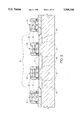
- FIG. 1 depicts the stacked storage node electrode of the related art comprising tantalum 1, platinum 2 (Ta/Pt) overlying the polysilicon plug 3.
- the sidewalls 4 of the tantalum film 1 formed during this process are subject to oxidation during the subsequent deposition of the BST layer. Since the tantalum 1 oxidizes the polysilicon plug 3 is also susceptible to oxidation. When portions of the polysilicon plug 3 and tantalum 1 are consumed by oxidation the capacitance of the storage cell capacitor is decreased since the storage node electrode is partially covered by a low dielectric constant film. Therefore the memory device cannot be made as dense.
- the storage node contact resistance increases-drastically between the polysilicon plug and the tantalum barrier layer as a result of degradation of the tantalum barrier layer during deposition of BST and other high dielectric constant materials.
- An object of the invention is to increase density of a memory device by increasing capacitance of storage cell capacitors.
- a further object of the invention is decreased contact resistance between a polysilicon electrode and a barrier layer and reduced degradation of the barrier layer.
- the storage cell capacitor of the invention features a storage node electrode having a barrier layer which prohibits diffusion of atoms.
- the barrier layer may be titanium nitride or another material which prohibits silicon diffusion.
- the barrier layer is interposed between a conductive plug and a non-oxidizing conductive material such as platinum.
- the barrier layer is surrounded on its sides by an insulative layer.
- the insulative layer and the non-oxidizing material protect the barrier layer from oxidizing during the deposition and anneal of the BST thereby also eliminating oxidation of the conductive plug. By eliminating oxidation of the barrier layer and the conductive plug capacitance is maximized, and the contact resistance is not affected.
- the invention also features a low contact resistance material lying between the conductive plug and the barrier layer.
- the invention is a storage node capacitor and a method for forming the storage node capacitor having a storage node electrode comprising a barrier layer interposed between a conductive plug and an oxidation resistant conductive layer.
- the method comprises forming the conductive plug in a thick layer of insulative material such as oxide or oxide/nitride.
- the conductive plug is recessed from a planarized top surface of the thick insulative layer.
- a low contact resistance material if formed at the base of the recess.
- the barrier layer is then formed in the recess.
- the process is continued with a formation of an oxidation resistant conductive layer and the patterning thereof to complete the formation of the storage node electrode.
- a dielectric layer typically having a high dielectric constant, is formed to overly the storage node electrode and a cell plate electrode is then fabricated to overly the dielectric layer.
- the barrier layer is protected during the formation of the dielectric layer by both the oxidation resistant conductive layer and the thick insulative layer there is no oxidation of the barrier layer or the contact plug thereby maximizing capacitance of the storage node and reducing high contact resistance issues.
- FIG. 1 is a cross-sectional view of a portion of a partially processed semiconductor wafer of the related art.
- FIGS. 2-11 are cross-sectional views of a portion of a partially processed semiconductor wafer depicting the steps of the invention for fabricating a storage cell capacitor.
- FIG. 2 depicts field-effect transistors overlying a silicon substrate and wordlines overlying field oxide.
- FIG. 3 is the wafer portion of FIG. 2 following the deposit of an undoped thick oxide layer and planarization thereof.
- FIG. 4 is the wafer portion of FIG. 3 following the masking and subsequent etching of the deposited oxide layer to form self-aligned openings.
- FIG. 5 is the wafer portion of FIG. 4 following the formation of polysilicon plugs in the openings and the removal of the mask shown in FIG. 4.
- FIG. 6 is the wafer portion of FIG. 5 following the recessing of the polysilicon plug in the thick oxide layer.
- FIG. 7 is the wafer portion of FIG. 6 following a deposition of titanium.
- FIG. 8 is the wafer portion of FIG. 7 following an anneal and removal of unreacted Titanium.
- FIGS. 9A and 9B are wafer portions of FIG. 8 following the deposition of a titanium nitride layer.
- FIGS. 10A and 10B are wafer portions of FIGS. 9A and B following the planarization of the titanium nitride layer.
- FIGS. 11A and 11B are wafer portions of FIGS. 10A and 10B following the deposition of a platinum layer.
- FIGS. 12A and 12B are the wafer portions of FIG. 11A and 11B, respectively, following the planarization of the platinum layer to complete the formation of the storage node.
- FIGS. 13A and 13B are wafer portions of FIGS. 12A and 12B, respectively, following the deposition of a BST dielectric layer and a cell plate layer and patterning of these layers to complete the formation of the storage cell capacitor.
- FIGS. 2-11 The method for fabricating the storage cell capacitor of the invention is shown pictorially in FIGS. 2-11.
- FIG. 2 a cross-sectional view of an inprocess dynamic random access memory (DRAM) cell is shown following conventional local oxidation of silicon (LOCOS) or special LOCOS processing which creates substantially planar field oxide regions 5 (created using modified LOCOS or trench isolation processes) and future active areas 6 (those regions of the substrate not covered by field oxide) on a silicon substrate 7.
- LOCOS local oxidation of silicon
- the creation of the field oxide is preceded or followed by a thermally grown dielectric layer 8 of silicon oxide.
- the depicted cell is one of many cells that are fabricated simultaneously and comprise a memory array.
- a first conductively doped polysilicon layer 10 a metal silicide layer (Wsi x ) 15, an oxide layer 16, and a thick nitride layer 20 are deposited.
- the thick nitride layer 20 will function as an etch stop during the storage node buried contact etch, thus allowing self-alignment if desired.
- the layers are patterned and etched to form wordlines 21 and N-channel (NCH) field effect transistors 22.
- the polysilicon layer 10 forms the gate regions of the FETs and is insulated from lightly-doped source/drain regions 25 by the dielectric layer 8.
- the lightly-doped regions 25 are created utilizing a phosphorus or arsenic implant.
- RIE reactive ion etch
- FETs 22 and wordlines 21 are exemplary of one application to be used in conjunction with the present embodiment of the invention. Other methods of fabrication and other applications are also feasible and perhaps equally viable.
- a thick insulative conformal layer of undoped oxide 40 is blanket deposited to fill the storage node areas and overlie the FETS 22 and wordlines 21.
- the oxide is undoped to minimize dopant out diffusion from the oxide 40 to the doped regions of the substrate.
- the oxide 40 is planarized, preferably chemical mechanically planarized (CMP), in order to provide a uniform height.
- CMP chemical mechanically planarized
- nitride, oxynitride or another suitable material may be deposited as the insulative layer.
- CMP involves holding or rotating a wafer of semiconductor material against a wetted polishing surface under controlled chemical slurry, pressure, and temperature conditions.
- a chemical slurry containing a polishing agent such as alumina or silica may be utilized as the abrasive medium. Additionally, the chemical slurry may contain chemical etchants. This procedure may be used to produce a surface with a desired endpoint or thickness, which also has a polished and planarized surface.
- buried digit lines may be fabricated as described in U.S. Pat. No. 5,168,073 herein incorporated by reference.
- the buried digit lines are formed by the method described in U.S. Pat. No. 5,168,073 an initial thick oxide layer is deposited and planarized and then overlaid with a relatively thick Si 3 N 4 layer which is also planarized.
- These two layers serve the same function as the oxide layer 40 and may be used in place of Oxide layer 40 even in the case where buried digit lines are not formed.
- the thick oxide is typically deposited prior to the digit line formation and the Si 3 N 4 is deposited subsequent to the digit line formation.
- the thick insulative layer is comprised only of oxide it is possible for oxygen to diffuse through the oxide. By overlying the oxide with Si 3 N 4 it is possible to prohibit oxygen diffusion though the oxide.
- mask 53 defines self-aligned substrate contact area 55.
- the oxide 40 is etched, preferably dry etched, to form a self-aligned openings 60 exposing the contact areas 55 of the substrate 7.
- a polysilicon plug 65 is formed in each opening 60.
- the actual method used to form the polysilicon plugs 65 is not critical, two options being a selective silicon growth from the contact area 55 or a in-situ doped polysilicon deposition and subsequent etch back or CMP back.
- an upper portion of the polysilicon plugs 65 is removed during a dry etch in order to form a recesses 70, Typically, this etch back is 50 to 400 nano meters (nm). In a case where the polysilicon plugs 65 are formed during a selective silicon growth it is possible to form the recess 70 by controlling the growth.
- a first barrier layer of titanium 66 is deposited to overly oxide 40 and polysilicon plug 65.
- a thermal anneal is performed and the titanium 66 in contact with the polysilicon plug reacts with the polysilicon to form titanium silicide. It is possible to perform the anneal in nitrogen. In this case the titanium still reacts with the polysilicon to form titanium silicide, and the titanium which is not in contact with the polysilicon plug reacts with the nitrogen to form TiN.
- a thin layer of nitrogen is formed overlying the titanium silicide.
- refractory metals may be used. These refractory metals may be chosen from the list of refractory metals comprising W, Co, Ta, and Mo.
- a metal nitride such as TiN
- TiN a metal nitride
- the refractory metal and the metal nitride are both capable of reacting with the polysilicon plug to form a silicide during an anneal.
- the unsilicided layer (the unreacted titanium in the case of a non-nitrogen anneal, or the TiN, in the case of a nitrogen anneal) and the thin nitrogen layer have been removed during a wet etch.
- the titanium silicide 67 overlying the polysilicon plug 65 is retained during the etch.
- a second barrier layer, titanium nitride layer 75 is formed by a chemical vapor deposition (CVD) or a sputtering process performed at room temperature.
- the titanium nitride layer 75 has a thickness greater than or equal to the depth of recess 70 remaining after the removal of the unreacted titanium 66.
- the titanium silicide layer lowers a contact resistance between the polysilicon plug 65 and the titanium nitride layer 75.
- the titanium nitride layer 75 provides a barrier against silicon diffusion of the polysilicon plug 65 and the titanium silicide layer 67 during subsequent high temperature anneals.
- titanium nitride Other materials capable of prohibiting silicon diffusion may be used in place-of titanium nitride. These materials may be chosen from refractory metals, conductive metal oxides or metal nitrides and must be capable of prohibiting silicon diffusion. Some examples include tantalum, TaN, Ti, RuO 2 and Ru.
- the titanium nitride layer 75 is formed such that its thickness is less than the depth of the recess 70 remaining after the removal of the unreacted titanium 66.
- the storage cell capacitor gains more vertical area thereby increasing capacitance.
- the titanium nitride layer 75 of FIGS. 9A and 9B is planarized, preferably by CMP, in order to expose at least the oxide layer 40 and in order to retain titanium nitride 75 in recesses 70 overlying the titanium silicide 67. Portions of the oxide layer 40 may be planarized during this step. It is important, of course to retain a sufficient depth of titanium nitride 75 in order to inhibit silicon diffusion. It can be seen that only the upper surface of the titanium nitride layer 75 is exposed and that the titanium nitride sidewalls 80 are protected by the oxide layer 40.
- a platinum layer 85 is formed at room temperature by CVD or a sputtering technique.
- the platinum layer 85 overlies the titanium nitride layer 75 shown in FIGS. 10A and 10B, respectively. Since the platinum layer 85 is resistant to oxidation it provides an excellent surface for the deposition of the high dielectric constant material. In addition, the platinum layer 85 protects the top surface of the titanium nitride layer 75 from strong oxidizing conditions during the BST deposition. Therefore platinum is used as the upper portion of the first electrode since it will not oxidize during a BST deposition or subsequent anneals.
- An electrode that oxidizes would have a low dielectric constant film below the BST, thereby negating the advantages provided by the high dielectric constant material.
- the titanium nitride layer is introduced to avoid Si and Pt inter-diffusion of atoms, thereby preventing the formation of SiO 2 of top of the platinum surface.
- Other materials which are resistant to oxidation may be used in place of the platinum.
- RuO 2 as well as other non-oxidizing materials may be used.
- TiN could also be used. However, TiN cannot be used in place of platinum.
- the titanium nitride layer is recessed in the oxide layer 40, a thick layer of platinum may be deposited without decreasing the density of the device.
- the capacitance area is increased by the sidewall area contribution. Therefore, the platinum is deposited from at least a thickness of 50 nm to a thickness of 1 micro meter ( ⁇ m).
- FIGS. 12A and 12B depict the structure following the masking of the platinum layer 85 overlying the titanium nitride and the removal of unmasked portions of the platinum layer 85 to form the completed storage node electrode of the storage cell capacitor.
- the unmasked platinum is removed during a dry etch using Hbr gas.
- the storage node electrode is thought of as comprising the titanium nitride layer 75 and the platinum layer 85.
- the polysilicon plug 65 is often thought of as an electrical interconnect interposed between the substrate and the storage node electrode, although it can be thought of as a portion of the storage node itself.
- FIGS. 13A and 13B depict the storage cell capacitor following a deposition and anneal of a dielectric layer 90 overlying the platinum layer 85 of FIGS. 12A and 12B, respectively.
- the dielectric layer is typified as having a high dielectric constant.
- the storage cell capacitor fabrication is completed with the sputter or CVD of a 50 to 200 nm thick cell plate layer 95 to form a cell plate electrode.
- the cell plate layer 95 is typically Platinum, TiN or some other conductive material.
- suitable materials for a dielectric layer having a high dielectric constant are Ba x Sr.sub.(1-x) TiO 3 [BST], BaTiO 3 , SrTiO 3 , PbTiO 3 , Pb(Zr,Ti)O 3 [PZT], (Pb,La)(Zr,Ti)O 3 [PLZT], (Pb,La)TiO 3 [PLT], KNO 3 , and LiNbO 3 .
- BST is the preferred material and is deposited at a thickness within the range of 30 nm-300nm by RF-magnetron sputtering or deposited by chemical vapor deposition (CVD) in a vapor environment at a temperature within the range of temperatures between 200 and 800 degrees Celsius.
- the actual vapor environment and temperature may vary for the specific dielectric being deposited. These variations are well known to those skilled in the art.
- the titanium nitride layer 75 is not oxidized during the application of a high temperature anneal due to the fact that it is protected from the vapor environment on its sidewalls 80 by the oxide layer 40 and that it is protected on its upper surface by the platinum layer 85, see FIGS. 11.
- the recess retains the original titanium nitride 75 formed therein and capacitance is not sacrificed as it would be when portions of the titanium nitride 75 are consumed by oxidation. Therefore capacitance is effectively increased over methods where portions of titanium nitride are oxidized.
- a high density memory device featuring a stacked capacitor formed in a compact area as a result of a dielectric layer having a high dielectric constant.
- the method of the invention provides retention of storage node integrity during an anneal of the dielectric layer.
Abstract
Description
Claims (27)
Priority Applications (8)
| Application Number | Priority Date | Filing Date | Title |
|---|---|---|---|
| US08/313,677 US5506166A (en) | 1993-04-02 | 1994-09-27 | Method for forming capacitor compatible with high dielectric constant materials having a low contact resistance layer |
| US08/572,846 US5959327A (en) | 1993-04-02 | 1995-12-14 | Capacitor compatible with high dielectric constant materials having a low contact resistance layer and the method for forming same |
| US09/362,326 US6531730B2 (en) | 1993-08-10 | 1999-07-27 | Capacitor compatible with high dielectric constant materials having a low contact resistance layer and the method for forming same |
| US10/386,337 US7015532B2 (en) | 1993-04-02 | 2003-03-10 | Capacitor compatible with high dielectric constant materials having a low contact resistance layer and the method for forming same |
| US10/939,928 US7153707B2 (en) | 1993-04-02 | 2004-09-13 | Method for forming a storage cell capacitor compatible with high dielectric constant materials |
| US11/216,415 US7402489B2 (en) | 1993-04-02 | 2005-08-30 | Capacitor compatible with high dielectric constant materials having a low contact resistance layer and the method for forming same |
| US11/458,072 US7398595B2 (en) | 1993-04-02 | 2006-07-17 | Method for forming a storage cell capacitor compatible with high dielectric constant materials |
| US11/726,143 US7393753B2 (en) | 1993-04-02 | 2007-03-21 | Method for forming a storage cell capacitor compatible with high dielectric constant materials |
Applications Claiming Priority (3)
| Application Number | Priority Date | Filing Date | Title |
|---|---|---|---|
| US4433193A | 1993-04-02 | 1993-04-02 | |
| US08/104,525 US5381302A (en) | 1993-04-02 | 1993-08-10 | Capacitor compatible with high dielectric constant materials having a low contact resistance layer and the method for forming same |
| US08/313,677 US5506166A (en) | 1993-04-02 | 1994-09-27 | Method for forming capacitor compatible with high dielectric constant materials having a low contact resistance layer |
Related Parent Applications (2)
| Application Number | Title | Priority Date | Filing Date |
|---|---|---|---|
| US4433193A Continuation-In-Part | 1993-04-02 | 1993-04-02 | |
| US08/104,525 Division US5381302A (en) | 1993-04-02 | 1993-08-10 | Capacitor compatible with high dielectric constant materials having a low contact resistance layer and the method for forming same |
Related Child Applications (3)
| Application Number | Title | Priority Date | Filing Date |
|---|---|---|---|
| US08/390,336 Continuation US5478772A (en) | 1993-04-02 | 1995-02-17 | Method for forming a storage cell capacitor compatible with high dielectric constant materials |
| US08/572,846 Continuation US5959327A (en) | 1993-04-02 | 1995-12-14 | Capacitor compatible with high dielectric constant materials having a low contact resistance layer and the method for forming same |
| US11/726,143 Continuation US7393753B2 (en) | 1993-04-02 | 2007-03-21 | Method for forming a storage cell capacitor compatible with high dielectric constant materials |
Publications (1)
| Publication Number | Publication Date |
|---|---|
| US5506166A true US5506166A (en) | 1996-04-09 |
Family
ID=26721412
Family Applications (3)
| Application Number | Title | Priority Date | Filing Date |
|---|---|---|---|
| US08/104,525 Expired - Lifetime US5381302A (en) | 1993-04-02 | 1993-08-10 | Capacitor compatible with high dielectric constant materials having a low contact resistance layer and the method for forming same |
| US08/313,677 Expired - Lifetime US5506166A (en) | 1993-04-02 | 1994-09-27 | Method for forming capacitor compatible with high dielectric constant materials having a low contact resistance layer |
| US08/572,846 Expired - Lifetime US5959327A (en) | 1993-04-02 | 1995-12-14 | Capacitor compatible with high dielectric constant materials having a low contact resistance layer and the method for forming same |
Family Applications Before (1)
| Application Number | Title | Priority Date | Filing Date |
|---|---|---|---|
| US08/104,525 Expired - Lifetime US5381302A (en) | 1993-04-02 | 1993-08-10 | Capacitor compatible with high dielectric constant materials having a low contact resistance layer and the method for forming same |
Family Applications After (1)
| Application Number | Title | Priority Date | Filing Date |
|---|---|---|---|
| US08/572,846 Expired - Lifetime US5959327A (en) | 1993-04-02 | 1995-12-14 | Capacitor compatible with high dielectric constant materials having a low contact resistance layer and the method for forming same |
Country Status (1)
| Country | Link |
|---|---|
| US (3) | US5381302A (en) |
Cited By (100)
| Publication number | Priority date | Publication date | Assignee | Title |
|---|---|---|---|---|
| US5714402A (en) * | 1995-11-30 | 1998-02-03 | Hyundai Electronics Industries Co., Ltd. | Method for fabricating a capacitor of a semiconductor device and the structure of the same |
| DE19640413A1 (en) * | 1996-09-30 | 1998-04-02 | Siemens Ag | Method for manufacturing barrier-free semiconductor memory devices |
| US5736449A (en) * | 1993-08-06 | 1998-04-07 | Hitachi, Ltd. | Semiconductor memory device having improved isolation between electrodes, and process for fabricating the same |
| WO1998015014A1 (en) * | 1996-09-30 | 1998-04-09 | Siemens Aktiengesellschaft | Capacitor with an electrode core and a thin noble metal layer used as a first electrode |
| WO1998015013A1 (en) * | 1996-09-30 | 1998-04-09 | Siemens Aktiengesellschaft | Semiconductor device with a protected barrier for a stack cell |
| US5744853A (en) * | 1995-09-15 | 1998-04-28 | Chartered Semiconductor Manufacturing Pte Ltd | Three dimensional polysilicon capacitor for high density integrated circuit applications |
| US5786259A (en) * | 1997-04-25 | 1998-07-28 | Samsung Electronics Co., Ltd. | Methods of forming integrated circuit capacitors including etch stopping layers |
| US5793600A (en) * | 1994-05-16 | 1998-08-11 | Texas Instruments Incorporated | Method for forming high dielectric capacitor electrode structure and semiconductor memory devices |
| US5796573A (en) * | 1997-05-29 | 1998-08-18 | International Business Machines Corporation | Overhanging separator for self-defining stacked capacitor |
| KR19980060624A (en) * | 1996-12-31 | 1998-10-07 | 김영환 | Capacitor Manufacturing Method of Semiconductor Device |
| US5843818A (en) * | 1995-12-05 | 1998-12-01 | Samsung Electronics Co., Ltd. | Methods of fabricating ferroelectric capacitors |
| US5854127A (en) * | 1997-03-13 | 1998-12-29 | Micron Technology, Inc. | Method of forming a contact landing pad |
| EP0887844A2 (en) * | 1997-06-27 | 1998-12-30 | Siemens Aktiengesellschaft | Method of manufacturing a barrier layer on top of a contact plug |
| US5871886A (en) * | 1996-12-12 | 1999-02-16 | Taiwan Semiconductor Manufacturing Company, Ltd. | Sandwiched middle antireflection coating (SMARC) process |
| US5874353A (en) * | 1997-07-31 | 1999-02-23 | United Microelectronics Corporation | Method of forming a self-aligned silicide device |
| US5896835A (en) * | 1996-01-10 | 1999-04-27 | Sanshin Kogyo Kabushiki Kaisha | Induction system for outboard motor |
| EP0926717A2 (en) | 1997-12-19 | 1999-06-30 | Siemens Aktiengesellschaft | Polysilicon capacitor electrode |
| US5955756A (en) * | 1997-05-29 | 1999-09-21 | International Business Machines Corporation | Trench separator for self-defining discontinuous film |
| US5959327A (en) * | 1993-04-02 | 1999-09-28 | Micron Technology, Inc. | Capacitor compatible with high dielectric constant materials having a low contact resistance layer and the method for forming same |
| KR100226772B1 (en) * | 1996-09-25 | 1999-10-15 | 김영환 | Semiconductor memory device and fabricating method thereof |
| US5970309A (en) * | 1995-09-19 | 1999-10-19 | Samsung Electronics Co., Ltd. | Method of manufacturing a capacitor and a capacitor electrode in semiconductor device |
| US5976976A (en) * | 1997-08-21 | 1999-11-02 | Micron Technology, Inc. | Method of forming titanium silicide and titanium by chemical vapor deposition |
| US5981331A (en) * | 1996-03-29 | 1999-11-09 | Mitsubishi Denki Kabushiki Kaisha | Method of manufacturing a semiconductor memory device with a high dielectric constant capacitor |
| GB2338106A (en) * | 1998-06-02 | 1999-12-08 | Samsung Electronics Co Ltd | A contact of a semiconductor device |
| US6002575A (en) * | 1997-05-29 | 1999-12-14 | International Business Machines Corporation | Adherent separator for self-defining discontinuous film |
| KR100235955B1 (en) * | 1996-06-27 | 1999-12-15 | 김영환 | Method for manufacturing capacitor semiconductor device |
| KR100239418B1 (en) * | 1996-12-03 | 2000-01-15 | 김영환 | Semiconductor device capacitor and manufacturing method thereof |
| KR100239417B1 (en) * | 1996-12-03 | 2000-01-15 | 김영환 | Capacitor of semiconductor device amd manufacturing method thereof |
| US6030847A (en) * | 1993-04-02 | 2000-02-29 | Micron Technology, Inc. | Method for forming a storage cell capacitor compatible with high dielectric constant materials |
| WO2000014796A1 (en) * | 1998-09-03 | 2000-03-16 | Micron Technology, Inc. | Method of forming a silicon contact interface |
| US6043529A (en) * | 1996-09-30 | 2000-03-28 | Siemens Aktiengesellschaft | Semiconductor configuration with a protected barrier for a stacked cell |
| US6051475A (en) * | 1998-06-03 | 2000-04-18 | Taiwan Semiconductor Manufacturing Company | Method for manufacturing a silicide to silicide capacitor |
| US6066528A (en) * | 1993-04-02 | 2000-05-23 | Micron Technology, Inc. | Method for forming a capacitor compatible with high dielectric constant materials having two independent insulative layers |
| US6093575A (en) * | 1996-09-04 | 2000-07-25 | Nippon Steel Corporation | Semiconductor device and production method of a semiconductor device having a capacitor |
| US6124626A (en) * | 1997-08-22 | 2000-09-26 | Micron Technology, Inc. | Capacitor structures formed using excess oxygen containing material provided relative to electrodes thereof |
| US6127214A (en) * | 1996-12-09 | 2000-10-03 | Texas Instruments Incorporated | Contact gate structure and method |
| US6130124A (en) * | 1996-12-04 | 2000-10-10 | Samsung Electronics Co., Ltd. | Methods of forming capacitor electrodes having reduced susceptibility to oxidation |
| KR100269301B1 (en) * | 1997-07-16 | 2000-10-16 | 윤종용 | Capacitor for preventing barrier layer from oxidizing and manufacturing method thereof |
| US6136716A (en) * | 1998-11-09 | 2000-10-24 | Worldwide Semiconductor Manufacturing Corporation | Method for manufacturing a self-aligned stacked storage node DRAM cell |
| US6143362A (en) * | 1998-02-25 | 2000-11-07 | Micron Technology, Inc. | Chemical vapor deposition of titanium |
| US6153491A (en) * | 1997-05-29 | 2000-11-28 | International Business Machines Corporation | Overhanging separator for self-defining discontinuous film |
| US6159791A (en) * | 1998-12-08 | 2000-12-12 | Hyundai Electronics Industries Co., Ltd. | Fabrication method of capacitor |
| US6162671A (en) * | 1997-12-06 | 2000-12-19 | Samsung Electronics, Co., Ltd. | Method of forming capacitors having high dielectric constant material |
| DE19926501A1 (en) * | 1999-06-10 | 2000-12-21 | Siemens Ag | Method of manufacturing a semiconductor memory device |
| KR100275113B1 (en) * | 1997-12-30 | 2001-01-15 | 김영환 | A method for fabricating ferroelectric capacitor in semiconductor device |
| KR100275116B1 (en) * | 1997-12-27 | 2001-01-15 | 김영환 | Method for forming capacitor of semiconductor device |
| US6175146B1 (en) | 1997-03-13 | 2001-01-16 | Micron Technology, Inc. | Semiconductor processing methods of forming integrated circuitry memory devices, methods of forming capacitor containers, methods of making electrical connection to circuit nodes and related integrated circuitry |
| US6177701B1 (en) * | 1996-01-04 | 2001-01-23 | Nec Corporation | Semiconductor device with resistor and fabrication method therof |
| KR100282431B1 (en) * | 1997-11-14 | 2001-03-02 | 김영환 | Method for forming capacitor of semiconductor device the same |
| US6211033B1 (en) * | 1996-01-23 | 2001-04-03 | Micron Technology, Inc. | Integrated capacitor bottom electrode for use with conformal dielectric |
| US6218296B1 (en) * | 1998-07-03 | 2001-04-17 | Samsung Electronics Co., Ltd. | Semiconductor device with pillar-shaped capacitor storage node and method of fabricating the same |
| US6218308B1 (en) * | 1999-04-30 | 2001-04-17 | Worldwide Semiconductor Manufacturing Corp. | Method of manufacturing a contact for a capacitor of high density DRAMs |
| US6218231B1 (en) * | 1997-12-27 | 2001-04-17 | Hyundai Electronics Industries Co., Ltd. | Methods for fabricating high dielectric capacitors of semiconductor devices |
| US6222217B1 (en) | 1997-11-27 | 2001-04-24 | Mitsubishi Denki Kabushiki Kaisha | Semiconductor device and manufacturing method thereof |
| US6239028B1 (en) | 1998-09-03 | 2001-05-29 | Micron Technology, Inc. | Methods for forming iridium-containing films on substrates |
| US6251720B1 (en) | 1996-09-27 | 2001-06-26 | Randhir P. S. Thakur | High pressure reoxidation/anneal of high dielectric constant materials |
| KR100292689B1 (en) * | 1998-06-03 | 2001-07-12 | 김영환 | Capacitor and Formation Method |
| US6271131B1 (en) | 1998-08-26 | 2001-08-07 | Micron Technology, Inc. | Methods for forming rhodium-containing layers such as platinum-rhodium barrier layers |
| US6284316B1 (en) | 1998-02-25 | 2001-09-04 | Micron Technology, Inc. | Chemical vapor deposition of titanium |
| US6284655B1 (en) | 1998-09-03 | 2001-09-04 | Micron Technology, Inc. | Method for producing low carbon/oxygen conductive layers |
| US6291363B1 (en) | 1999-03-01 | 2001-09-18 | Micron Technology, Inc. | Surface treatment of DARC films to reduce defects in subsequent cap layers |
| US6303956B1 (en) | 1999-02-26 | 2001-10-16 | Micron Technology, Inc. | Conductive container structures having a dielectric cap |
| US6309973B1 (en) * | 1998-02-27 | 2001-10-30 | Micron Technology, Inc. | Semiconductor processing methods of forming a conductive projection and methods of increasing alignment tolerances |
| US6319764B1 (en) | 1999-08-25 | 2001-11-20 | Micron Technology, Inc. | Method of forming haze-free BST films |
| US6323081B1 (en) | 1998-09-03 | 2001-11-27 | Micron Technology, Inc. | Diffusion barrier layers and methods of forming same |
| US6329286B1 (en) | 1999-04-27 | 2001-12-11 | Micron Technology, Inc. | Methods for forming conformal iridium layers on substrates |
| US6344965B1 (en) * | 1999-03-16 | 2002-02-05 | Hyundai Electronics Industries Co., Ltd. | Capacitor using high dielectric constant film for semiconductor memory device and fabrication method therefor |
| KR20020011479A (en) * | 2000-08-02 | 2002-02-09 | 박종섭 | The method of fabricating metal-line in semiconductor device |
| US6358793B1 (en) | 1999-02-26 | 2002-03-19 | Micron Technology, Inc. | Method for localized masking for semiconductor structure development |
| US6376297B1 (en) | 1998-03-20 | 2002-04-23 | Micron Technology, Inc. | Latch-up prevention for memory cells |
| US6417537B1 (en) | 2000-01-18 | 2002-07-09 | Micron Technology, Inc. | Metal oxynitride capacitor barrier layer |
| US6445023B1 (en) | 1999-03-16 | 2002-09-03 | Micron Technology, Inc. | Mixed metal nitride and boride barrier layers |
| KR100351451B1 (en) * | 1999-12-30 | 2002-09-09 | 주식회사 하이닉스반도체 | Method for forming capacitor of memory device |
| US6465828B2 (en) | 1999-07-30 | 2002-10-15 | Micron Technology, Inc. | Semiconductor container structure with diffusion barrier |
| US6476432B1 (en) | 2000-03-23 | 2002-11-05 | Micron Technology, Inc. | Structures and methods for enhancing capacitors in integrated circuits |
| US6503803B2 (en) * | 1995-11-14 | 2003-01-07 | Hitachi, Ltd. | Method of fabricating a semiconductor integrated circuit device for connecting semiconductor region and electrical wiring metal via titanium silicide layer |
| US6531730B2 (en) | 1993-08-10 | 2003-03-11 | Micron Technology, Inc. | Capacitor compatible with high dielectric constant materials having a low contact resistance layer and the method for forming same |
| US20030157757A1 (en) * | 1996-05-30 | 2003-08-21 | Takahiro Kumauchi | Method of manufacturing a semiconductor integrated circuit device |
| US6639266B1 (en) | 2000-08-30 | 2003-10-28 | Micron Technology, Inc. | Modifying material removal selectivity in semiconductor structure development |
| US20030207556A1 (en) * | 1998-02-26 | 2003-11-06 | Weimer Ronald A. | Forming a conductive structure in a semiconductor device |
| US6660631B1 (en) | 2000-08-31 | 2003-12-09 | Micron Technology, Inc. | Devices containing platinum-iridium films and methods of preparing such films and devices |
| US6673670B1 (en) | 1998-11-23 | 2004-01-06 | Micron Technology, Inc. | Method of forming a capacitor structure and DRAM circuitry having a capacitor structure including interior areas spaced apart from one another in a non-overlapping relationship |
| US20040041236A1 (en) * | 2002-08-29 | 2004-03-04 | Micron Technology, Inc. | Merged mos-bipolar capacitor memory cell |
| KR100424710B1 (en) * | 2001-11-21 | 2004-03-27 | 주식회사 하이닉스반도체 | Fabricating method of semiconductor device |
| US20040097034A1 (en) * | 2000-06-07 | 2004-05-20 | Sandhu Gurtej S. | Capacitor structure |
| US6750110B1 (en) | 1998-07-23 | 2004-06-15 | Micron Technology, Inc. | Continuous good step coverage CVD platinum metal deposition |
| US6791131B1 (en) | 1993-04-02 | 2004-09-14 | Micron Technology, Inc. | Method for forming a storage cell capacitor compatible with high dielectric constant materials |
| US6804142B2 (en) | 2002-11-12 | 2004-10-12 | Micron Technology, Inc. | 6F2 3-transistor DRAM gain cell |
| KR100464652B1 (en) * | 2002-11-25 | 2004-12-31 | 주식회사 하이닉스반도체 | Method for forming capacitor of semiconductor device |
| US20050024936A1 (en) * | 2003-03-04 | 2005-02-03 | Micron Technology, Inc. | Vertical gain cell |
| US20050041457A1 (en) * | 2002-08-29 | 2005-02-24 | Micron Technology, Inc. | Single transistor vertical memory gain cell |
| US20050074149A1 (en) * | 2003-10-03 | 2005-04-07 | Confirma, Inc. | System and method for hierarchical analysis of contrast enhanced medical imaging information |
| US20050093093A1 (en) * | 2003-10-30 | 2005-05-05 | Edmund Burke | Capacitor integration at top-metal level with a protective cladding for copper surface protection |
| US20050287736A1 (en) * | 2004-06-16 | 2005-12-29 | Porter John D | Latch-up prevention for memory cells |
| KR100559720B1 (en) * | 1999-09-10 | 2006-03-10 | 주식회사 하이닉스반도체 | Method of manufacturing a capacitor in a semiconductor device |
| KR100481831B1 (en) * | 1997-07-24 | 2006-05-16 | 삼성전자주식회사 | Capacitor Manufacturing Method for Semiconductor Devices |
| US20070254473A1 (en) * | 2006-04-28 | 2007-11-01 | Hynix Semiconductor Inc. | Method for fabricating semiconductor device |
| KR100791345B1 (en) | 2006-10-02 | 2008-01-03 | 삼성전자주식회사 | Semiconductor device including a recessed spherical silicide contact portion and method of manufacturing the same |
| US20090176361A1 (en) * | 2005-02-03 | 2009-07-09 | Samsung Electronics Co., Ltd. | Semiconductor device preventing electrical short and method of manufacturing the same |
| US20130102148A1 (en) * | 2007-03-23 | 2013-04-25 | Taiwan Semiconductor Manufacturing Company, Ltd. | Interconnect Structure for Semiconductor Devices |
Families Citing this family (54)
| Publication number | Priority date | Publication date | Assignee | Title |
|---|---|---|---|---|
| US5439840A (en) * | 1993-08-02 | 1995-08-08 | Motorola, Inc. | Method of forming a nonvolatile random access memory capacitor cell having a metal-oxide dielectric |
| KR0171060B1 (en) * | 1993-12-28 | 1999-03-30 | 스기야마 카즈히코 | Manufacturing method of semiconductor device |
| US5622893A (en) * | 1994-08-01 | 1997-04-22 | Texas Instruments Incorporated | Method of forming conductive noble-metal-insulator-alloy barrier layer for high-dielectric-constant material electrodes |
| US5489548A (en) * | 1994-08-01 | 1996-02-06 | Texas Instruments Incorporated | Method of forming high-dielectric-constant material electrodes comprising sidewall spacers |
| US6093615A (en) | 1994-08-15 | 2000-07-25 | Micron Technology, Inc. | Method of fabricating a contact structure having a composite barrier layer between a platinum layer and a polysilicon plug |
| US5464786A (en) * | 1994-10-24 | 1995-11-07 | Micron Technology, Inc. | Method for forming a capacitor having recessed lateral reaction barrier layer edges |
| KR100190558B1 (en) * | 1995-03-04 | 1999-10-15 | 구본준 | Ferroelectric and capacitor of semiconductor device |
| US5668040A (en) * | 1995-03-20 | 1997-09-16 | Lg Semicon Co., Ltd. | Method for forming a semiconductor device electrode which also serves as a diffusion barrier |
| EP0739030A3 (en) * | 1995-04-19 | 1998-07-08 | Nec Corporation | Highly-integrated thin film capacitor with high dielectric constant layer |
| US6455916B1 (en) | 1996-04-08 | 2002-09-24 | Micron Technology, Inc. | Integrated circuit devices containing isolated dielectric material |
| US6660610B2 (en) | 1996-07-08 | 2003-12-09 | Micron Technology, Inc. | Devices having improved capacitance and methods of their fabrication |
| US6080645A (en) * | 1996-10-29 | 2000-06-27 | Micron Technology, Inc. | Method of making a doped silicon diffusion barrier region |
| US5932907A (en) * | 1996-12-24 | 1999-08-03 | International Business Machines Corporation | Method, materials, and structures for noble metal electrode contacts to silicon |
| US6294420B1 (en) | 1997-01-31 | 2001-09-25 | Texas Instruments Incorporated | Integrated circuit capacitor |
| US5926730A (en) * | 1997-02-19 | 1999-07-20 | Micron Technology, Inc. | Conductor layer nitridation |
| US6015997A (en) | 1997-02-19 | 2000-01-18 | Micron Technology, Inc. | Semiconductor structure having a doped conductive layer |
| US6262458B1 (en) | 1997-02-19 | 2001-07-17 | Micron Technology, Inc. | Low resistivity titanium silicide structures |
| JP2988413B2 (en) * | 1997-02-20 | 1999-12-13 | 日本電気株式会社 | Semiconductor device and manufacturing method thereof |
| KR19990003495A (en) * | 1997-06-25 | 1999-01-15 | 김영환 | Barrier metal layer formation method of semiconductor device |
| KR100437353B1 (en) * | 1997-07-16 | 2004-07-16 | 삼성전자주식회사 | Method of manufacturing semiconductor device using upper bonding metal film for protecting upper electrode from over-etch |
| US6150691A (en) | 1997-12-19 | 2000-11-21 | Micron Technology, Inc. | Spacer patterned, high dielectric constant capacitor |
| US6344413B1 (en) | 1997-12-22 | 2002-02-05 | Motorola Inc. | Method for forming a semiconductor device |
| US6143617A (en) * | 1998-02-23 | 2000-11-07 | Taiwan Semiconductor Manufacturing Company | Composite capacitor electrode for a DRAM cell |
| US5998258A (en) * | 1998-04-22 | 1999-12-07 | Motorola, Inc. | Method of forming a semiconductor device having a stacked capacitor structure |
| US6046059A (en) * | 1998-05-08 | 2000-04-04 | Siemens Aktiengesellschaft | Method of forming stack capacitor with improved plug conductivity |
| US6541812B2 (en) | 1998-06-19 | 2003-04-01 | Micron Technology, Inc. | Capacitor and method for forming the same |
| US5985731A (en) * | 1998-08-17 | 1999-11-16 | Motorola, Inc. | Method for forming a semiconductor device having a capacitor structure |
| US6486060B2 (en) * | 1998-09-03 | 2002-11-26 | Micron Technology, Inc. | Low resistance semiconductor process and structures |
| US6184129B1 (en) * | 1998-09-29 | 2001-02-06 | Texas Instruments Incorporated | Low resistivity poly-silicon gate produced by selective metal growth |
| US6222220B1 (en) * | 1998-12-10 | 2001-04-24 | Siemens Aktiengesellschaft | Extended trench for preventing interaction between components of stacked capacitors |
| JP2000349255A (en) * | 1999-06-03 | 2000-12-15 | Oki Electric Ind Co Ltd | Semiconductor storage device and manufacture thereof |
| US6419554B2 (en) * | 1999-06-24 | 2002-07-16 | Micron Technology, Inc. | Fixed abrasive chemical-mechanical planarization of titanium nitride |
| DE19950540B4 (en) * | 1999-10-20 | 2005-07-21 | Infineon Technologies Ag | Process for the preparation of a capacitor electrode with barrier structure |
| US7253076B1 (en) * | 2000-06-08 | 2007-08-07 | Micron Technologies, Inc. | Methods for forming and integrated circuit structures containing ruthenium and tungsten containing layers |
| US6482736B1 (en) | 2000-06-08 | 2002-11-19 | Micron Technology, Inc. | Methods for forming and integrated circuit structures containing enhanced-surface-area conductive layers |
| US6429127B1 (en) | 2000-06-08 | 2002-08-06 | Micron Technology, Inc. | Methods for forming rough ruthenium-containing layers and structures/methods using same |
| US6455424B1 (en) * | 2000-08-07 | 2002-09-24 | Micron Technology, Inc. | Selective cap layers over recessed polysilicon plugs |
| US7307021B1 (en) * | 2000-10-02 | 2007-12-11 | National Semiconductor Corporation | Method for planarizing a thin film |
| US7192827B2 (en) * | 2001-01-05 | 2007-03-20 | Micron Technology, Inc. | Methods of forming capacitor structures |
| US6511873B2 (en) * | 2001-06-15 | 2003-01-28 | International Business Machines Corporation | High-dielectric constant insulators for FEOL capacitors |
| FR2828766B1 (en) * | 2001-08-16 | 2004-01-16 | St Microelectronics Sa | INTEGRATED CIRCUIT COMPRISING ACTIVE ELEMENTS AND AT LEAST ONE PASSIVE ELEMENT, IN PARTICULAR DRAM MEMORY CELLS AND MANUFACTURING METHOD |
| US6596580B2 (en) * | 2001-10-18 | 2003-07-22 | Infineon Technologies Ag | Recess Pt structure for high k stacked capacitor in DRAM and FRAM, and the method to form this structure |
| JP2003289134A (en) * | 2002-03-28 | 2003-10-10 | Matsushita Electric Ind Co Ltd | Semiconductor device and manufacturing method therefor |
| US7119024B2 (en) * | 2003-07-10 | 2006-10-10 | Micron Technology, Inc. | Method and structure for a self-aligned silicided word line and polysilicon plug during the formation of a semiconductor device |
| KR20050011151A (en) * | 2003-07-22 | 2005-01-29 | 삼성전자주식회사 | Methods of forming semiconductor device having a capacitor including electrodes comprising metal |
| KR100738066B1 (en) * | 2003-12-01 | 2007-07-12 | 삼성전자주식회사 | Method of forming silicide film having excellent thermal stability, semiconductor device and semiconductor memory device comprising silicide film formed by the same, and methods of manufacturing the same |
| KR100668833B1 (en) * | 2004-12-17 | 2007-01-16 | 주식회사 하이닉스반도체 | Emthod for fabricating capacitor in semiconductor device |
| KR100724568B1 (en) * | 2005-10-12 | 2007-06-04 | 삼성전자주식회사 | Semiconductor memory device and method of fabricating the same |
| US20080122032A1 (en) * | 2006-08-16 | 2008-05-29 | Taiwan Semiconductor Manufacturing Co., Ltd. | Semiconductor devices with MIM-type decoupling capacitors and fabrication method thereof |
| US7629256B2 (en) | 2007-05-14 | 2009-12-08 | Asm International N.V. | In situ silicon and titanium nitride deposition |
| US7833906B2 (en) | 2008-12-11 | 2010-11-16 | Asm International N.V. | Titanium silicon nitride deposition |
| JP2011129762A (en) * | 2009-12-18 | 2011-06-30 | Elpida Memory Inc | Semiconductor device and method of manufacturing the same |
| US8436404B2 (en) | 2009-12-30 | 2013-05-07 | Intel Corporation | Self-aligned contacts |
| US8896030B2 (en) | 2012-09-07 | 2014-11-25 | Intel Corporation | Integrated circuits with selective gate electrode recess |
Citations (5)
| Publication number | Priority date | Publication date | Assignee | Title |
|---|---|---|---|---|
| EP0494313A1 (en) * | 1990-07-24 | 1992-07-15 | Seiko Epson Corporation | Semiconductor device provided with ferroelectric material |
| US5187638A (en) * | 1992-07-27 | 1993-02-16 | Micron Technology, Inc. | Barrier layers for ferroelectric and pzt dielectric on silicon |
| US5198384A (en) * | 1991-05-15 | 1993-03-30 | Micron Technology, Inc. | Process for manufacturing a ferroelectric dynamic/non-volatile memory array using a disposable layer above storage-node junction |
| US5335138A (en) * | 1993-02-12 | 1994-08-02 | Micron Semiconductor, Inc. | High dielectric constant capacitor and method of manufacture |
| US5366920A (en) * | 1993-04-12 | 1994-11-22 | Nec Corporation | Method for fabricating a thin film capacitor |
Family Cites Families (27)
| Publication number | Priority date | Publication date | Assignee | Title |
|---|---|---|---|---|
| JPS61296764A (en) * | 1985-06-25 | 1986-12-27 | Mitsubishi Electric Corp | Semiconductor device with metal electrode wiring film |
| JPS63312613A (en) * | 1987-06-15 | 1988-12-21 | Nec Corp | Single plate capacitor |
| US4782309A (en) * | 1987-06-26 | 1988-11-01 | The United States Of America As Represented By The Secretary Of The Army | Bilateral frequency adjustment of crystal oscillators |
| US5046043A (en) * | 1987-10-08 | 1991-09-03 | National Semiconductor Corporation | Ferroelectric capacitor and memory cell including barrier and isolation layers |
| US5189503A (en) * | 1988-03-04 | 1993-02-23 | Kabushiki Kaisha Toshiba | High dielectric capacitor having low current leakage |
| US5235199A (en) * | 1988-03-25 | 1993-08-10 | Kabushiki Kaisha Toshiba | Semiconductor memory with pad electrode and bit line under stacked capacitor |
| KR950000156B1 (en) * | 1989-02-08 | 1995-01-10 | 세이꼬 엡슨 가부시끼가이샤 | Semiconductor device |
| JP2537413B2 (en) * | 1989-03-14 | 1996-09-25 | 三菱電機株式会社 | Semiconductor device and manufacturing method thereof |
| JPH02273934A (en) * | 1989-04-17 | 1990-11-08 | Oki Electric Ind Co Ltd | Semiconductor element and manufacture thereof |
| US5005102A (en) * | 1989-06-20 | 1991-04-02 | Ramtron Corporation | Multilayer electrodes for integrated circuit capacitors |
| US4982309A (en) * | 1989-07-17 | 1991-01-01 | National Semiconductor Corporation | Electrodes for electrical ceramic oxide devices |
| DE69017802T2 (en) * | 1989-08-30 | 1995-09-07 | Nec Corp | Thin film capacitor and its manufacturing process. |
| US5248628A (en) * | 1989-09-08 | 1993-09-28 | Kabushiki Kaisha Toshiba | Method of fabricating a semiconductor memory device |
| DE69123422T2 (en) * | 1990-04-24 | 1997-06-05 | Ramtron Int Corp | SEMICONDUCTOR ARRANGEMENT WITH FERROELECTRIC MATERIAL AND METHOD FOR THE PRODUCTION THEREOF |
| US5098860A (en) * | 1990-05-07 | 1992-03-24 | The Boeing Company | Method of fabricating high-density interconnect structures having tantalum/tantalum oxide layers |
| US5111355A (en) * | 1990-09-13 | 1992-05-05 | National Semiconductor Corp. | High value tantalum oxide capacitor |
| JPH04177760A (en) * | 1990-11-09 | 1992-06-24 | Matsushita Electric Ind Co Ltd | Semiconductor storage device and its manufacture |
| US5053351A (en) * | 1991-03-19 | 1991-10-01 | Micron Technology, Inc. | Method of making stacked E-cell capacitor DRAM cell |
| US5168073A (en) * | 1991-10-31 | 1992-12-01 | Micron Technology, Inc. | Method for fabricating storage node capacitor having tungsten and etched tin storage node capacitor plate |
| US5401680A (en) * | 1992-02-18 | 1995-03-28 | National Semiconductor Corporation | Method for forming a ceramic oxide capacitor having barrier layers |
| US5391511A (en) * | 1992-02-19 | 1995-02-21 | Micron Technology, Inc. | Semiconductor processing method of producing an isolated polysilicon lined cavity and a method of forming a capacitor |
| US5162248A (en) * | 1992-03-13 | 1992-11-10 | Micron Technology, Inc. | Optimized container stacked capacitor DRAM cell utilizing sacrificial oxide deposition and chemical mechanical polishing |
| US5185689A (en) * | 1992-04-29 | 1993-02-09 | Motorola Inc. | Capacitor having a ruthenate electrode and method of formation |
| US5392189A (en) * | 1993-04-02 | 1995-02-21 | Micron Semiconductor, Inc. | Capacitor compatible with high dielectric constant materials having two independent insulative layers and the method for forming same |
| US5381302A (en) * | 1993-04-02 | 1995-01-10 | Micron Semiconductor, Inc. | Capacitor compatible with high dielectric constant materials having a low contact resistance layer and the method for forming same |
| US5340765A (en) * | 1993-08-13 | 1994-08-23 | Micron Semiconductor, Inc. | Method for forming enhanced capacitance stacked capacitor structures using hemi-spherical grain polysilicon |
| US5631804A (en) * | 1995-11-13 | 1997-05-20 | Micron Technology, Inc. | Contact fill capacitor having a sidewall that connects the upper and lower surfaces of the dielectric and partially surrounds an insulating layer |
-
1993
- 1993-08-10 US US08/104,525 patent/US5381302A/en not_active Expired - Lifetime
-
1994
- 1994-09-27 US US08/313,677 patent/US5506166A/en not_active Expired - Lifetime
-
1995
- 1995-12-14 US US08/572,846 patent/US5959327A/en not_active Expired - Lifetime
Patent Citations (5)
| Publication number | Priority date | Publication date | Assignee | Title |
|---|---|---|---|---|
| EP0494313A1 (en) * | 1990-07-24 | 1992-07-15 | Seiko Epson Corporation | Semiconductor device provided with ferroelectric material |
| US5198384A (en) * | 1991-05-15 | 1993-03-30 | Micron Technology, Inc. | Process for manufacturing a ferroelectric dynamic/non-volatile memory array using a disposable layer above storage-node junction |
| US5187638A (en) * | 1992-07-27 | 1993-02-16 | Micron Technology, Inc. | Barrier layers for ferroelectric and pzt dielectric on silicon |
| US5335138A (en) * | 1993-02-12 | 1994-08-02 | Micron Semiconductor, Inc. | High dielectric constant capacitor and method of manufacture |
| US5366920A (en) * | 1993-04-12 | 1994-11-22 | Nec Corporation | Method for fabricating a thin film capacitor |
Cited By (260)
| Publication number | Priority date | Publication date | Assignee | Title |
|---|---|---|---|---|
| US7253052B2 (en) | 1993-04-02 | 2007-08-07 | Micron Technology, Inc. | Method for forming a storage cell capacitor compatible with high dielectric constant materials |
| US7385240B2 (en) | 1993-04-02 | 2008-06-10 | Micron Technology, Inc. | Storage cell capacitor compatible with high dielectric constant materials |
| US20030155604A1 (en) * | 1993-04-02 | 2003-08-21 | Micron Technology, Inc. | Capacitor compatible with high dielectric constant materials having a low contact resistance layer and the method for forming same |
| US7402489B2 (en) * | 1993-04-02 | 2008-07-22 | Micron Technology, Inc. | Capacitor compatible with high dielectric constant materials having a low contact resistance layer and the method for forming same |
| US6762924B2 (en) | 1993-04-02 | 2004-07-13 | Micron Technology, Inc. | Capacitor compatible with high dielectric constant materials having two independent insulative layers and the method for forming same |
| US7393753B2 (en) | 1993-04-02 | 2008-07-01 | Micron Technology, Inc. | Method for forming a storage cell capacitor compatible with high dielectric constant materials |
| US7015532B2 (en) | 1993-04-02 | 2006-03-21 | Micron Technology, Inc. | Capacitor compatible with high dielectric constant materials having a low contact resistance layer and the method for forming same |
| US6791131B1 (en) | 1993-04-02 | 2004-09-14 | Micron Technology, Inc. | Method for forming a storage cell capacitor compatible with high dielectric constant materials |
| US20060001019A1 (en) * | 1993-04-02 | 2006-01-05 | Micron Technology, Inc. | Capacitor compatible with high dielectric constant materials having a low contact resistance layer and the method for forming same |
| US20050104107A1 (en) * | 1993-04-02 | 2005-05-19 | Micron Technology, Inc. | Method for forming a storage cell capacitor compatible with high dielectric constant materials |
| US6030847A (en) * | 1993-04-02 | 2000-02-29 | Micron Technology, Inc. | Method for forming a storage cell capacitor compatible with high dielectric constant materials |
| US20050003609A1 (en) * | 1993-04-02 | 2005-01-06 | Micron Technology, Inc. | Method for forming a storage cell capacitor compatible with high dielectric constant materials |
| US6495427B2 (en) * | 1993-04-02 | 2002-12-17 | Micron Technology, Inc. | Method for forming a capacitor compatible with high dielectric constant materials having two independent insulative layers |
| US6066528A (en) * | 1993-04-02 | 2000-05-23 | Micron Technology, Inc. | Method for forming a capacitor compatible with high dielectric constant materials having two independent insulative layers |
| US7153707B2 (en) | 1993-04-02 | 2006-12-26 | Micron Technology, Inc. | Method for forming a storage cell capacitor compatible with high dielectric constant materials |
| US20070166915A1 (en) * | 1993-04-02 | 2007-07-19 | Micron Technology, Inc. | Method for forming a storage cell capacitor compatible with high dielectric constant materials |
| US5959327A (en) * | 1993-04-02 | 1999-09-28 | Micron Technology, Inc. | Capacitor compatible with high dielectric constant materials having a low contact resistance layer and the method for forming same |
| US5736449A (en) * | 1993-08-06 | 1998-04-07 | Hitachi, Ltd. | Semiconductor memory device having improved isolation between electrodes, and process for fabricating the same |
| US6531730B2 (en) | 1993-08-10 | 2003-03-11 | Micron Technology, Inc. | Capacitor compatible with high dielectric constant materials having a low contact resistance layer and the method for forming same |
| US5793600A (en) * | 1994-05-16 | 1998-08-11 | Texas Instruments Incorporated | Method for forming high dielectric capacitor electrode structure and semiconductor memory devices |
| US5744853A (en) * | 1995-09-15 | 1998-04-28 | Chartered Semiconductor Manufacturing Pte Ltd | Three dimensional polysilicon capacitor for high density integrated circuit applications |
| US5970309A (en) * | 1995-09-19 | 1999-10-19 | Samsung Electronics Co., Ltd. | Method of manufacturing a capacitor and a capacitor electrode in semiconductor device |
| US6503803B2 (en) * | 1995-11-14 | 2003-01-07 | Hitachi, Ltd. | Method of fabricating a semiconductor integrated circuit device for connecting semiconductor region and electrical wiring metal via titanium silicide layer |
| US5714402A (en) * | 1995-11-30 | 1998-02-03 | Hyundai Electronics Industries Co., Ltd. | Method for fabricating a capacitor of a semiconductor device and the structure of the same |
| US5843818A (en) * | 1995-12-05 | 1998-12-01 | Samsung Electronics Co., Ltd. | Methods of fabricating ferroelectric capacitors |
| US6177701B1 (en) * | 1996-01-04 | 2001-01-23 | Nec Corporation | Semiconductor device with resistor and fabrication method therof |
| US5896835A (en) * | 1996-01-10 | 1999-04-27 | Sanshin Kogyo Kabushiki Kaisha | Induction system for outboard motor |
| US6555432B2 (en) | 1996-01-23 | 2003-04-29 | Micron Technology, Inc. | Integrated capacitor bottom electrode for use with conformal dielectric |
| US6838338B2 (en) | 1996-01-23 | 2005-01-04 | Micron Technology, Inc. | Integrated capacitor bottom electrode for use with conformal dielectric |
| US6211033B1 (en) * | 1996-01-23 | 2001-04-03 | Micron Technology, Inc. | Integrated capacitor bottom electrode for use with conformal dielectric |
| US20030153145A1 (en) * | 1996-01-23 | 2003-08-14 | Sandhu Gurtej S. | Integrated capacitor bottom electrode for use with conformal dielectric |
| US5981331A (en) * | 1996-03-29 | 1999-11-09 | Mitsubishi Denki Kabushiki Kaisha | Method of manufacturing a semiconductor memory device with a high dielectric constant capacitor |
| US20030157757A1 (en) * | 1996-05-30 | 2003-08-21 | Takahiro Kumauchi | Method of manufacturing a semiconductor integrated circuit device |
| US6852579B2 (en) * | 1996-05-30 | 2005-02-08 | Hitachi, Ltd. | Method of manufacturing a semiconductor integrated circuit device |
| KR100235955B1 (en) * | 1996-06-27 | 1999-12-15 | 김영환 | Method for manufacturing capacitor semiconductor device |
| US6093575A (en) * | 1996-09-04 | 2000-07-25 | Nippon Steel Corporation | Semiconductor device and production method of a semiconductor device having a capacitor |
| KR100226772B1 (en) * | 1996-09-25 | 1999-10-15 | 김영환 | Semiconductor memory device and fabricating method thereof |
| US6794703B1 (en) | 1996-09-27 | 2004-09-21 | Micron Technology, Inc. | High pressure reoxidation/anneal of high dielectric constant |
| US6251720B1 (en) | 1996-09-27 | 2001-06-26 | Randhir P. S. Thakur | High pressure reoxidation/anneal of high dielectric constant materials |
| US6486020B1 (en) | 1996-09-27 | 2002-11-26 | Micron Technology, Inc. | High pressure reoxidation/anneal of high dielectric constant materials |
| US6605505B2 (en) | 1996-09-30 | 2003-08-12 | Siemens Aktiengesellschaft | Process for producing an integrated semiconductor memory configuration |
| JP2001501375A (en) * | 1996-09-30 | 2001-01-30 | シーメンス アクチエンゲゼルシヤフト | Semiconductor device having a protective barrier against staple cells |
| DE19640413A1 (en) * | 1996-09-30 | 1998-04-02 | Siemens Ag | Method for manufacturing barrier-free semiconductor memory devices |
| WO1998015013A1 (en) * | 1996-09-30 | 1998-04-09 | Siemens Aktiengesellschaft | Semiconductor device with a protected barrier for a stack cell |
| US6297526B1 (en) | 1996-09-30 | 2001-10-02 | Siemens Aktiengesellschaft | Process for producing barrier-free semiconductor memory configurations |
| WO1998015014A1 (en) * | 1996-09-30 | 1998-04-09 | Siemens Aktiengesellschaft | Capacitor with an electrode core and a thin noble metal layer used as a first electrode |
| KR100442892B1 (en) * | 1996-09-30 | 2004-08-02 | 지멘스 악티엔게젤샤프트 | Semiconductor device with a protected barrier for a stack cell |
| US6043529A (en) * | 1996-09-30 | 2000-03-28 | Siemens Aktiengesellschaft | Semiconductor configuration with a protected barrier for a stacked cell |
| KR100239418B1 (en) * | 1996-12-03 | 2000-01-15 | 김영환 | Semiconductor device capacitor and manufacturing method thereof |
| KR100239417B1 (en) * | 1996-12-03 | 2000-01-15 | 김영환 | Capacitor of semiconductor device amd manufacturing method thereof |
| US6130124A (en) * | 1996-12-04 | 2000-10-10 | Samsung Electronics Co., Ltd. | Methods of forming capacitor electrodes having reduced susceptibility to oxidation |
| US6127214A (en) * | 1996-12-09 | 2000-10-03 | Texas Instruments Incorporated | Contact gate structure and method |
| US5871886A (en) * | 1996-12-12 | 1999-02-16 | Taiwan Semiconductor Manufacturing Company, Ltd. | Sandwiched middle antireflection coating (SMARC) process |
| KR19980060624A (en) * | 1996-12-31 | 1998-10-07 | 김영환 | Capacitor Manufacturing Method of Semiconductor Device |
| US6281070B1 (en) | 1997-03-13 | 2001-08-28 | Micron Technology, Inc. | Semiconductor processing methods of forming integrated circuitry memory devices, methods of forming capacitor containers, methods of making electrical connection to circuit nodes and related integrated circuitry |
| US6424043B1 (en) | 1997-03-13 | 2002-07-23 | Micron Technology, Inc. | Semiconductor processing methods of forming integrated circuitry memory devices, methods of forming capacitor containers, methods of making electrical connection to circuit nodes and related integrated circuitry |
| US6583002B2 (en) | 1997-03-13 | 2003-06-24 | Micron Technology, Inc. | Semiconductor processing methods of forming integrated circuitry memory devices, methods of forming capacitor containers, methods of making electrical connection to circuit nodes and related integrated circuitry |
| US6611018B2 (en) | 1997-03-13 | 2003-08-26 | Micron Technology, Inc. | Semiconductor processing methods of forming integrated circuitry memory devices, methods of forming capacitor containers, methods of making electrical connection to circuit nodes and related integrated circuitry |
| US6261899B1 (en) * | 1997-03-13 | 2001-07-17 | Micron Technology, Inc. | Semiconductor processing methods of forming integrated circuitry memory devices, methods of forming capacitor containers, methods of making electrical connection to circuit nodes and related integrated circuitry |
| US6175146B1 (en) | 1997-03-13 | 2001-01-16 | Micron Technology, Inc. | Semiconductor processing methods of forming integrated circuitry memory devices, methods of forming capacitor containers, methods of making electrical connection to circuit nodes and related integrated circuitry |
| US5854127A (en) * | 1997-03-13 | 1998-12-29 | Micron Technology, Inc. | Method of forming a contact landing pad |
| US6495410B2 (en) | 1997-03-13 | 2002-12-17 | Micron Technology, Inc. | Semiconductor processing methods of forming integrated circuitry memory devices, methods of forming capacitor containers, methods of making electrical connection to circuit nodes and related integrated circuitry |
| US6653187B2 (en) | 1997-03-13 | 2003-11-25 | Micron Technology, Inc. | Semiconductor processing methods |
| US5786259A (en) * | 1997-04-25 | 1998-07-28 | Samsung Electronics Co., Ltd. | Methods of forming integrated circuit capacitors including etch stopping layers |
| US5796573A (en) * | 1997-05-29 | 1998-08-18 | International Business Machines Corporation | Overhanging separator for self-defining stacked capacitor |
| US5955756A (en) * | 1997-05-29 | 1999-09-21 | International Business Machines Corporation | Trench separator for self-defining discontinuous film |
| US6191469B1 (en) | 1997-05-29 | 2001-02-20 | International Business Machines Corporation | Overhanging separator for self-defining discontinuous film |
| US6268259B1 (en) | 1997-05-29 | 2001-07-31 | International Business Machines Corporation | Overhanging separator for self-defining stacked capacitor |
| US6002575A (en) * | 1997-05-29 | 1999-12-14 | International Business Machines Corporation | Adherent separator for self-defining discontinuous film |
| US6153491A (en) * | 1997-05-29 | 2000-11-28 | International Business Machines Corporation | Overhanging separator for self-defining discontinuous film |
| US6150230A (en) * | 1997-05-29 | 2000-11-21 | International Business Machines Corporation | Trench separator for self-defining discontinuous film |
| EP0887844A3 (en) * | 1997-06-27 | 2000-07-26 | Siemens Aktiengesellschaft | Method of manufacturing a barrier layer on top of a contact plug |
| EP0887844A2 (en) * | 1997-06-27 | 1998-12-30 | Siemens Aktiengesellschaft | Method of manufacturing a barrier layer on top of a contact plug |
| US6100187A (en) * | 1997-06-27 | 2000-08-08 | Siemens Aktiengesellschaft | Method of producing a barrier layer in a semiconductor body |
| KR100269301B1 (en) * | 1997-07-16 | 2000-10-16 | 윤종용 | Capacitor for preventing barrier layer from oxidizing and manufacturing method thereof |
| KR100481831B1 (en) * | 1997-07-24 | 2006-05-16 | 삼성전자주식회사 | Capacitor Manufacturing Method for Semiconductor Devices |
| US5874353A (en) * | 1997-07-31 | 1999-02-23 | United Microelectronics Corporation | Method of forming a self-aligned silicide device |
| US6255209B1 (en) | 1997-08-21 | 2001-07-03 | Micron Technology, Inc. | Methods of forming a contact having titanium formed by chemical vapor deposition |
| US6171943B1 (en) | 1997-08-21 | 2001-01-09 | Micron, Technology, Inc. | Methods of forming a contact having titanium silicide formed by chemical vapor deposition |
| US6208033B1 (en) | 1997-08-21 | 2001-03-27 | Micron Technology Inc. | Apparatus having titanium silicide and titanium formed by chemical vapor deposition |
| US6255216B1 (en) | 1997-08-21 | 2001-07-03 | Micron Technology, Inc. | Methods of forming a contact having titanium silicide and titanium formed by chemical vapor deposition |
| US6472756B2 (en) | 1997-08-21 | 2002-10-29 | Micron Technology, Inc. | Method of forming titanium silicide and titanium by chemical vapor deposition and resulting apparatus |
| US5976976A (en) * | 1997-08-21 | 1999-11-02 | Micron Technology, Inc. | Method of forming titanium silicide and titanium by chemical vapor deposition |
| US6376327B2 (en) | 1997-08-22 | 2002-04-23 | Micron Technology, Inc. | Structures formed using excess oxygen containing material |
| US20040166646A1 (en) * | 1997-08-22 | 2004-08-26 | Micron Technology, Inc. | Methods for use in forming a capacitor and structures resulting from same |
| US6200874B1 (en) | 1997-08-22 | 2001-03-13 | Micron Technology, Inc. | Methods for use in forming a capacitor |
| US6124626A (en) * | 1997-08-22 | 2000-09-26 | Micron Technology, Inc. | Capacitor structures formed using excess oxygen containing material provided relative to electrodes thereof |
| US6890814B2 (en) | 1997-08-22 | 2005-05-10 | Micron Technology, Inc. | Methods for use in forming a capacitor and structures resulting from same |
| US6696745B2 (en) | 1997-08-22 | 2004-02-24 | Micron Technology, Inc. | Methods for use in forming a capacitor and structures resulting from same |
| KR100282431B1 (en) * | 1997-11-14 | 2001-03-02 | 김영환 | Method for forming capacitor of semiconductor device the same |
| US6222217B1 (en) | 1997-11-27 | 2001-04-24 | Mitsubishi Denki Kabushiki Kaisha | Semiconductor device and manufacturing method thereof |
| US6162671A (en) * | 1997-12-06 | 2000-12-19 | Samsung Electronics, Co., Ltd. | Method of forming capacitors having high dielectric constant material |
| EP0926717A2 (en) | 1997-12-19 | 1999-06-30 | Siemens Aktiengesellschaft | Polysilicon capacitor electrode |
| EP0926717A3 (en) * | 1997-12-19 | 2003-04-02 | Siemens Aktiengesellschaft | Polysilicon capacitor electrode |
| US6218231B1 (en) * | 1997-12-27 | 2001-04-17 | Hyundai Electronics Industries Co., Ltd. | Methods for fabricating high dielectric capacitors of semiconductor devices |
| KR100275116B1 (en) * | 1997-12-27 | 2001-01-15 | 김영환 | Method for forming capacitor of semiconductor device |
| KR100275113B1 (en) * | 1997-12-30 | 2001-01-15 | 김영환 | A method for fabricating ferroelectric capacitor in semiconductor device |
| US6284316B1 (en) | 1998-02-25 | 2001-09-04 | Micron Technology, Inc. | Chemical vapor deposition of titanium |
| US7443032B2 (en) | 1998-02-25 | 2008-10-28 | Micron Technology, Inc. | Memory device with chemical vapor deposition of titanium for titanium silicide contacts |
| US6143362A (en) * | 1998-02-25 | 2000-11-07 | Micron Technology, Inc. | Chemical vapor deposition of titanium |
| US20050255698A1 (en) * | 1998-02-25 | 2005-11-17 | Micron Technology, Inc. | Chemical vapor deposition of titanim |
| US6433434B1 (en) | 1998-02-25 | 2002-08-13 | Micron Technology, Inc. | Apparatus having a titanium alloy layer |
| US6903462B2 (en) | 1998-02-25 | 2005-06-07 | Micron Technology, Inc. | Chemical vapor deposition of titanium |
| US6940172B2 (en) | 1998-02-25 | 2005-09-06 | Micron Technology, Inc. | Chemical vapor deposition of titanium |
| US8456007B2 (en) | 1998-02-25 | 2013-06-04 | Round Rock Research, Llc | Chemical vapor deposition of titanium |
| US20090039517A1 (en) * | 1998-02-25 | 2009-02-12 | Micron Technology, Inc. | Chemical vapor deposition of titanium |
| US6830820B2 (en) | 1998-02-25 | 2004-12-14 | Micron Technology, Inc. | Chemical vapor deposition of titanium |
| US6830838B2 (en) | 1998-02-25 | 2004-12-14 | Micron Technology, Inc. | Chemical vapor deposition of titanium |
| US20030207556A1 (en) * | 1998-02-26 | 2003-11-06 | Weimer Ronald A. | Forming a conductive structure in a semiconductor device |
| US6849544B2 (en) * | 1998-02-26 | 2005-02-01 | Micron Technology, Inc. | Forming a conductive structure in a semiconductor device |
| US6309973B1 (en) * | 1998-02-27 | 2001-10-30 | Micron Technology, Inc. | Semiconductor processing methods of forming a conductive projection and methods of increasing alignment tolerances |
| US6559057B2 (en) | 1998-02-27 | 2003-05-06 | Micron Technology, Inc. | Semiconductor processing methods of forming a conductive projection and methods of increasing alignment tolerances |
| US6376297B1 (en) | 1998-03-20 | 2002-04-23 | Micron Technology, Inc. | Latch-up prevention for memory cells |
| US20040223378A1 (en) * | 1998-03-20 | 2004-11-11 | Porter John D. | Latch-up prevention for memory cells |
| US6767784B2 (en) | 1998-03-20 | 2004-07-27 | Micron Technology, Inc. | Latch-up prevention for memory cells |
| US6642588B1 (en) | 1998-03-20 | 2003-11-04 | Micron Technology, Inc. | Latch-up prevention for memory cells |
| US7018889B2 (en) | 1998-03-20 | 2006-03-28 | Micron Technology, Inc. | Latch-up prevention for memory cells |
| CN1107969C (en) * | 1998-06-02 | 2003-05-07 | 三星电子株式会社 | Method for fabricating contact of semiconductor device |
| GB2338106B (en) * | 1998-06-02 | 2000-08-02 | Samsung Electronics Co Ltd | Method for fabricating a contact of a semiconductor device |
| GB2338106A (en) * | 1998-06-02 | 1999-12-08 | Samsung Electronics Co Ltd | A contact of a semiconductor device |
| US6051475A (en) * | 1998-06-03 | 2000-04-18 | Taiwan Semiconductor Manufacturing Company | Method for manufacturing a silicide to silicide capacitor |
| KR100292689B1 (en) * | 1998-06-03 | 2001-07-12 | 김영환 | Capacitor and Formation Method |
| US6218296B1 (en) * | 1998-07-03 | 2001-04-17 | Samsung Electronics Co., Ltd. | Semiconductor device with pillar-shaped capacitor storage node and method of fabricating the same |
| US6750110B1 (en) | 1998-07-23 | 2004-06-15 | Micron Technology, Inc. | Continuous good step coverage CVD platinum metal deposition |
| US6861693B2 (en) | 1998-07-23 | 2005-03-01 | Micron Technology, Inc. | Continuous good step coverage CVD platinum metal deposition |
| US6271131B1 (en) | 1998-08-26 | 2001-08-07 | Micron Technology, Inc. | Methods for forming rhodium-containing layers such as platinum-rhodium barrier layers |
| US6690055B1 (en) | 1998-08-26 | 2004-02-10 | Micron Technology, Inc. | Devices containing platinum-rhodium layers and methods |
| US20040147086A1 (en) * | 1998-08-26 | 2004-07-29 | Micron Technology, Inc. | Methods and apparatus for forming rhodium-containing layers |
| US7226861B2 (en) | 1998-08-26 | 2007-06-05 | Micron Technology, Inc. | Methods and apparatus for forming rhodium-containing layers |
| US7393785B2 (en) | 1998-08-26 | 2008-07-01 | Micron Technology, Inc. | Methods and apparatus for forming rhodium-containing layers |
| US20050260823A9 (en) * | 1998-08-26 | 2005-11-24 | Micron Technology, Inc. | Methods and apparatus for forming rhodium-containing layers |
| US7256123B2 (en) * | 1998-09-03 | 2007-08-14 | Micron Technology, Inc. | Method of forming an interface for a semiconductor device |
| US6323511B1 (en) | 1998-09-03 | 2001-11-27 | Micron Technology, Inc. | Structures including low carbon/oxygen conductive layers |
| US6323081B1 (en) | 1998-09-03 | 2001-11-27 | Micron Technology, Inc. | Diffusion barrier layers and methods of forming same |
| US6239028B1 (en) | 1998-09-03 | 2001-05-29 | Micron Technology, Inc. | Methods for forming iridium-containing films on substrates |
| US6284655B1 (en) | 1998-09-03 | 2001-09-04 | Micron Technology, Inc. | Method for producing low carbon/oxygen conductive layers |
| US20040175920A1 (en) * | 1998-09-03 | 2004-09-09 | Derderian Garo J. | Interface and method of forming an interface for a silicon contact |
| US6403414B2 (en) * | 1998-09-03 | 2002-06-11 | Micron Technology, Inc. | Method for producing low carbon/oxygen conductive layers |
| US6780758B1 (en) * | 1998-09-03 | 2004-08-24 | Micron Technology, Inc. | Method of establishing electrical contact between a semiconductor substrate and a semiconductor device |
| WO2000014796A1 (en) * | 1998-09-03 | 2000-03-16 | Micron Technology, Inc. | Method of forming a silicon contact interface |
| US20020146902A1 (en) * | 1998-09-03 | 2002-10-10 | Micron Technology, Inc. | Chemical vapor deposition apparatus |
| US6426292B2 (en) | 1998-09-03 | 2002-07-30 | Micron Technology, Inc. | Methods for forming iridium and platinum containing films on substrates |
| US6495458B2 (en) | 1998-09-03 | 2002-12-17 | Micron Technology, Inc. | Method for producing low carbon/oxygen conductive layers |
| US6136716A (en) * | 1998-11-09 | 2000-10-24 | Worldwide Semiconductor Manufacturing Corporation | Method for manufacturing a self-aligned stacked storage node DRAM cell |
| US6673670B1 (en) | 1998-11-23 | 2004-01-06 | Micron Technology, Inc. | Method of forming a capacitor structure and DRAM circuitry having a capacitor structure including interior areas spaced apart from one another in a non-overlapping relationship |
| US7071058B2 (en) | 1998-11-23 | 2006-07-04 | Micron Technology, Inc. | Methods of forming capacitors, and methods of forming DRAM circuitry |
| US6822848B2 (en) | 1998-11-23 | 2004-11-23 | Micron Technology, Inc. | Dynamic random access memory (DRAM) circuitry |
| US6717201B2 (en) * | 1998-11-23 | 2004-04-06 | Micron Technology, Inc. | Capacitor structure |
| US20040190223A1 (en) * | 1998-11-23 | 2004-09-30 | Roberts Martin Ceredig | Dynamic random access memory (DRAM) circuitry |
| US20040190222A1 (en) * | 1998-11-23 | 2004-09-30 | Roberts Martin Ceredig | Methods of forming capacitors, and methods of forming DRAM circuitry |
| US6159791A (en) * | 1998-12-08 | 2000-12-12 | Hyundai Electronics Industries Co., Ltd. | Fabrication method of capacitor |
| US6946357B2 (en) | 1999-02-26 | 2005-09-20 | Micron Technology, Inc. | Conductive container structures having a dielectric cap |
| US20060006448A1 (en) * | 1999-02-26 | 2006-01-12 | Micron Technology, Inc. | Localized masking for semiconductor structure development |
| US20030205749A1 (en) * | 1999-02-26 | 2003-11-06 | Micron Technology, Inc. | Localized masking for semiconductor structure development |
| US7868369B2 (en) | 1999-02-26 | 2011-01-11 | Micron Technology, Inc. | Localized masking for semiconductor structure development |
| US7298000B2 (en) | 1999-02-26 | 2007-11-20 | Micron Technology, Inc. | Conductive container structures having a dielectric cap |
| US7015529B2 (en) | 1999-02-26 | 2006-03-21 | Micron Technology, Inc. | Localized masking for semiconductor structure development |
| US20090102018A1 (en) * | 1999-02-26 | 2009-04-23 | Micron Technology, Inc. | Localized masking for semiconductor structure development |
| US20070284638A1 (en) * | 1999-02-26 | 2007-12-13 | Micron Technology, Inc. | Conductive container structures having a dielectric cap |
| US20020030220A1 (en) * | 1999-02-26 | 2002-03-14 | Micron Technology, Inc. | Conductive container structures having a dielectric cap |
| US6303956B1 (en) | 1999-02-26 | 2001-10-16 | Micron Technology, Inc. | Conductive container structures having a dielectric cap |
| US20060244030A1 (en) * | 1999-02-26 | 2006-11-02 | Micron Technology, Inc. | Conductive container structures having a dielectric cap |
| US6833579B2 (en) | 1999-02-26 | 2004-12-21 | Micron Technology, Inc. | Conductive container structures having a dielectric cap |
| US6358793B1 (en) | 1999-02-26 | 2002-03-19 | Micron Technology, Inc. | Method for localized masking for semiconductor structure development |
| US6573554B2 (en) | 1999-02-26 | 2003-06-03 | Micron Technology, Inc. | Localized masking for semiconductor structure development |
| US7468534B2 (en) | 1999-02-26 | 2008-12-23 | Micron Technology, Inc. | Localized masking for semiconductor structure development |
| US7199415B2 (en) | 1999-02-26 | 2007-04-03 | Micron Technology, Inc. | Conductive container structures having a dielectric cap |
| US6734518B2 (en) | 1999-03-01 | 2004-05-11 | Micron Technology, Inc. | Surface treatment of DARC films to reduce defects in subsequent cap layers |
| US6291363B1 (en) | 1999-03-01 | 2001-09-18 | Micron Technology, Inc. | Surface treatment of DARC films to reduce defects in subsequent cap layers |
| US6445023B1 (en) | 1999-03-16 | 2002-09-03 | Micron Technology, Inc. | Mixed metal nitride and boride barrier layers |
| US6664159B2 (en) | 1999-03-16 | 2003-12-16 | Micron Technology, Inc. | Mixed metal nitride and boride barrier layers |
| US6645811B2 (en) | 1999-03-16 | 2003-11-11 | Hyundai Electronics Industries Co., Ltd. | Capacitor using high dielectric constant film for semiconductor memory device and fabrication method therefor |
| US20070045856A1 (en) * | 1999-03-16 | 2007-03-01 | Vaartstra Brian A | Mixed metal nitride and boride barrier layers |
| US20040053495A1 (en) * | 1999-03-16 | 2004-03-18 | Vaartstra Brian A. | Method of forming barrier layers |
| US7101779B2 (en) | 1999-03-16 | 2006-09-05 | Micron, Technology, Inc. | Method of forming barrier layers |
| US6344965B1 (en) * | 1999-03-16 | 2002-02-05 | Hyundai Electronics Industries Co., Ltd. | Capacitor using high dielectric constant film for semiconductor memory device and fabrication method therefor |
| US6329286B1 (en) | 1999-04-27 | 2001-12-11 | Micron Technology, Inc. | Methods for forming conformal iridium layers on substrates |
| US6218308B1 (en) * | 1999-04-30 | 2001-04-17 | Worldwide Semiconductor Manufacturing Corp. | Method of manufacturing a contact for a capacitor of high density DRAMs |
| US6566220B2 (en) | 1999-06-10 | 2003-05-20 | Infineon Technologies Ag | Method for fabricating a semiconductor memory component |
| DE19926501A1 (en) * | 1999-06-10 | 2000-12-21 | Siemens Ag | Method of manufacturing a semiconductor memory device |
| US6780706B2 (en) * | 1999-07-30 | 2004-08-24 | Micron Technology, Inc. | Semiconductor container structure with diffusion barrier |
| US6465828B2 (en) | 1999-07-30 | 2002-10-15 | Micron Technology, Inc. | Semiconductor container structure with diffusion barrier |
| US6855971B2 (en) | 1999-08-25 | 2005-02-15 | Micron Technology, Inc. | Haze-free BST films |
| US6852593B2 (en) | 1999-08-25 | 2005-02-08 | Micron Technology, Inc. | Haze-free BST films |
| US20040063335A1 (en) * | 1999-08-25 | 2004-04-01 | Cem Basceri | Haze-free BST films |
| US6924968B2 (en) | 1999-08-25 | 2005-08-02 | Micron Technology, Inc. | Haze-free BST films |
| US6660535B2 (en) | 1999-08-25 | 2003-12-09 | Micronbtechnology, Inc. | Method of forming haze- free BST films |
| US6939723B2 (en) | 1999-08-25 | 2005-09-06 | Micron Technology, Inc. | Method of forming haze-free BST films |
| US6319764B1 (en) | 1999-08-25 | 2001-11-20 | Micron Technology, Inc. | Method of forming haze-free BST films |
| US20040038477A1 (en) * | 1999-08-25 | 2004-02-26 | Cem Basceri | Haze-free BST films |
| KR100559720B1 (en) * | 1999-09-10 | 2006-03-10 | 주식회사 하이닉스반도체 | Method of manufacturing a capacitor in a semiconductor device |
| KR100351451B1 (en) * | 1999-12-30 | 2002-09-09 | 주식회사 하이닉스반도체 | Method for forming capacitor of memory device |
| US6417537B1 (en) | 2000-01-18 | 2002-07-09 | Micron Technology, Inc. | Metal oxynitride capacitor barrier layer |
| US7002202B2 (en) | 2000-01-18 | 2006-02-21 | Micron Technology, Inc. | Metal oxynitride capacitor barrier layer |
| US6664584B2 (en) | 2000-01-18 | 2003-12-16 | Micron Technology, Inc. | Metal oxynitride capacitor barrier layer |
| US20040085802A1 (en) * | 2000-01-18 | 2004-05-06 | Micron Technology, Inc. | Metal oxynitride capacitor barrier layer |
| US7015527B2 (en) | 2000-01-18 | 2006-03-21 | Micron Technology, Inc. | Metal oxynitride capacitor barrier layer |
| US6670256B2 (en) | 2000-01-18 | 2003-12-30 | Micron Technology, Inc. | Metal oxynitride capacitor barrier layer |
| US6631069B2 (en) | 2000-01-18 | 2003-10-07 | Micron Technology, Inc. | Metal oxynitride capacitor barrier layer |
| US6664583B2 (en) | 2000-01-18 | 2003-12-16 | Micron Technology, Inc. | Metal oxynitride capacitor barrier layer |
| US6696716B2 (en) | 2000-03-23 | 2004-02-24 | Micron Technology, Inc. | Structures and methods for enhancing capacitors in integrated ciruits |
| US6476432B1 (en) | 2000-03-23 | 2002-11-05 | Micron Technology, Inc. | Structures and methods for enhancing capacitors in integrated circuits |
| US6861330B2 (en) | 2000-03-23 | 2005-03-01 | Micron Technology Inc. | Structures and methods for enhancing capacitors in integrated circuits |
| US20040097034A1 (en) * | 2000-06-07 | 2004-05-20 | Sandhu Gurtej S. | Capacitor structure |
| US20060258113A1 (en) * | 2000-06-07 | 2006-11-16 | Micron Technology, Inc. | Capacitor structure |
| US8421140B2 (en) | 2000-06-07 | 2013-04-16 | Micron Technology, Inc. | Dielectric structures |
| KR20020011479A (en) * | 2000-08-02 | 2002-02-09 | 박종섭 | The method of fabricating metal-line in semiconductor device |
| US6639266B1 (en) | 2000-08-30 | 2003-10-28 | Micron Technology, Inc. | Modifying material removal selectivity in semiconductor structure development |
| US6660631B1 (en) | 2000-08-31 | 2003-12-09 | Micron Technology, Inc. | Devices containing platinum-iridium films and methods of preparing such films and devices |
| US7217970B2 (en) | 2000-08-31 | 2007-05-15 | Micron Technology, Inc. | Devices containing platinum-iridium films and methods of preparing such films and devices |
| US20040048467A1 (en) * | 2000-08-31 | 2004-03-11 | Micron Technologies, Inc. | Devices containing platinum-iridium films and methods of preparing such films and devices |
| US20050006689A1 (en) * | 2000-08-31 | 2005-01-13 | Micron Technology, Inc. | Devices containing platinum-iridium films and methods of preparing such films and devices |
| US6900107B2 (en) * | 2000-08-31 | 2005-05-31 | Micron Technology, Inc. | Devices containing platinum-iridium films and methods of preparing such films and devices |
| KR100424710B1 (en) * | 2001-11-21 | 2004-03-27 | 주식회사 하이닉스반도체 | Fabricating method of semiconductor device |
| US7323380B2 (en) | 2002-08-29 | 2008-01-29 | Micron Technology, Inc. | Single transistor vertical memory gain cell |
| US7608876B2 (en) | 2002-08-29 | 2009-10-27 | Micron Technology, Inc. | Merged MOS-bipolar capacitor memory cell |
| US20060231879A1 (en) * | 2002-08-29 | 2006-10-19 | Micron Technology, Inc. | Merged MOS-bipolar capacitor memory cell |
| US20040041236A1 (en) * | 2002-08-29 | 2004-03-04 | Micron Technology, Inc. | Merged mos-bipolar capacitor memory cell |
| US20050265069A1 (en) * | 2002-08-29 | 2005-12-01 | Micron Technology, Inc. | Merged mos-bipolar capacitor memory cell |
| US7149109B2 (en) | 2002-08-29 | 2006-12-12 | Micron Technology, Inc. | Single transistor vertical memory gain cell |
| US7199417B2 (en) | 2002-08-29 | 2007-04-03 | Micron Technology, Inc. | Merged MOS-bipolar capacitor memory cell |
| US6943083B2 (en) | 2002-08-29 | 2005-09-13 | Micron Technology, Inc. | Merged MOS-bipolar capacitor memory cell |
| US7564087B2 (en) | 2002-08-29 | 2009-07-21 | Micron Technology, Inc. | Merged MOS-bipolar capacitor memory cell |
| US6940761B2 (en) | 2002-08-29 | 2005-09-06 | Micron Technology, Inc. | Merged MOS-bipolar capacitor memory cell |
| US6838723B2 (en) | 2002-08-29 | 2005-01-04 | Micron Technology, Inc. | Merged MOS-bipolar capacitor memory cell |
| US20050068828A1 (en) * | 2002-08-29 | 2005-03-31 | Micron Technology, Inc. | Merged MOS-bipolar capacitor memory cell |
| US20060252206A1 (en) * | 2002-08-29 | 2006-11-09 | Micron Technology, Inc. | Single transistor vertical memory gain cell |
| US20050041457A1 (en) * | 2002-08-29 | 2005-02-24 | Micron Technology, Inc. | Single transistor vertical memory gain cell |
| US20050094453A1 (en) * | 2002-08-29 | 2005-05-05 | Micron Technology, Inc. | Merged MOS-bipolar capacitor memory cell |
| US6975531B2 (en) | 2002-11-12 | 2005-12-13 | Micron Technology, Inc. | 6F2 3-transistor DRAM gain cell |
| US7151690B2 (en) | 2002-11-12 | 2006-12-19 | Micron Technology, Inc. | 6F2 3-Transistor DRAM gain cell |
| US20050012130A1 (en) * | 2002-11-12 | 2005-01-20 | Micron Technology, Inc. | 6F2 3-Transistor DRAM gain cell |
| US20060028859A1 (en) * | 2002-11-12 | 2006-02-09 | Micron Technology, Inc. | 6F2 3-Transistor DRAM gain cell |
| US6804142B2 (en) | 2002-11-12 | 2004-10-12 | Micron Technology, Inc. | 6F2 3-transistor DRAM gain cell |
| KR100464652B1 (en) * | 2002-11-25 | 2004-12-31 | 주식회사 하이닉스반도체 | Method for forming capacitor of semiconductor device |
| US20070158722A1 (en) * | 2003-03-04 | 2007-07-12 | Micron Technology, Inc. | Vertical gain cell |
| US20050024936A1 (en) * | 2003-03-04 | 2005-02-03 | Micron Technology, Inc. | Vertical gain cell |
| US20050032313A1 (en) * | 2003-03-04 | 2005-02-10 | Micron Technology, Inc. | Vertical gain cell |
| US7298638B2 (en) | 2003-03-04 | 2007-11-20 | Micron Technology, Inc. | Operating an electronic device having a vertical gain cell that includes vertical MOS transistors |
| US7528440B2 (en) | 2003-03-04 | 2009-05-05 | Micron Technology, Inc. | Vertical gain cell |
| US7241658B2 (en) | 2003-03-04 | 2007-07-10 | Micron Technology, Inc. | Vertical gain cell |
| US20050074149A1 (en) * | 2003-10-03 | 2005-04-07 | Confirma, Inc. | System and method for hierarchical analysis of contrast enhanced medical imaging information |
| US20100117195A1 (en) * | 2003-10-30 | 2010-05-13 | Texas Instruments Incorporated | Capacitor integration at top-metal level with a protective cladding for copper surface protection |
| US20050093093A1 (en) * | 2003-10-30 | 2005-05-05 | Edmund Burke | Capacitor integration at top-metal level with a protective cladding for copper surface protection |
| US8604587B2 (en) | 2003-10-30 | 2013-12-10 | Texas Instruments Incorporated | Capacitor integration at top-metal level with a protective cladding for copper surface protection |
| US7674682B2 (en) * | 2003-10-30 | 2010-03-09 | Texas Instruments Incorporated | Capacitor integration at top-metal level with a protective cladding for copper surface protection |
| US20050286288A1 (en) * | 2004-06-16 | 2005-12-29 | Porter John D | Latch-up prevention for memory cells |
| US20060128090A1 (en) * | 2004-06-16 | 2006-06-15 | Porter John D | Latch-up prevention for memory cells |
| US20050287736A1 (en) * | 2004-06-16 | 2005-12-29 | Porter John D | Latch-up prevention for memory cells |
| US7190610B2 (en) | 2004-06-16 | 2007-03-13 | Micron Technology, Inc. | Latch-up prevention for memory cells |
| US7754596B2 (en) * | 2005-02-03 | 2010-07-13 | Samsung Electronics Co., Ltd. | Semiconductor device preventing electrical short and method of manufacturing the same |
| US20090176361A1 (en) * | 2005-02-03 | 2009-07-09 | Samsung Electronics Co., Ltd. | Semiconductor device preventing electrical short and method of manufacturing the same |
| US20070254473A1 (en) * | 2006-04-28 | 2007-11-01 | Hynix Semiconductor Inc. | Method for fabricating semiconductor device |
| US7435677B2 (en) * | 2006-04-28 | 2008-10-14 | Hynix Semiconductor Inc. | Method for fabricating semiconductor device |
| US20080079090A1 (en) * | 2006-10-02 | 2008-04-03 | Samsung Electronics Co., Ltd. | Semiconductor device including recessed spherical silicide contact part and method of manufacturing the same |
| KR100791345B1 (en) | 2006-10-02 | 2008-01-03 | 삼성전자주식회사 | Semiconductor device including a recessed spherical silicide contact portion and method of manufacturing the same |
| US8785324B2 (en) * | 2007-03-23 | 2014-07-22 | Taiwan Semiconductor Manufacturing Company, Ltd. | Interconnect structure for semiconductor devices |
| US20130102148A1 (en) * | 2007-03-23 | 2013-04-25 | Taiwan Semiconductor Manufacturing Company, Ltd. | Interconnect Structure for Semiconductor Devices |
| US8999842B2 (en) | 2007-03-23 | 2015-04-07 | Taiwan Semiconductor Manufacturing Company, Ltd. | Interconnect structure for semiconductor devices |
| US9219036B2 (en) | 2007-03-23 | 2015-12-22 | Taiwan Semiconductor Manufacturing Company, Ltd. | Interconnect structure for semiconductor devices |
Also Published As
| Publication number | Publication date |
|---|---|
| US5959327A (en) | 1999-09-28 |
| US5381302A (en) | 1995-01-10 |
Similar Documents
| Publication | Publication Date | Title |
|---|---|---|
| US5506166A (en) | Method for forming capacitor compatible with high dielectric constant materials having a low contact resistance layer | |
| US6066528A (en) | Method for forming a capacitor compatible with high dielectric constant materials having two independent insulative layers | |
| US7402489B2 (en) | Capacitor compatible with high dielectric constant materials having a low contact resistance layer and the method for forming same | |
| US7393753B2 (en) | Method for forming a storage cell capacitor compatible with high dielectric constant materials | |
| US5478772A (en) | Method for forming a storage cell capacitor compatible with high dielectric constant materials | |
| US6030847A (en) | Method for forming a storage cell capacitor compatible with high dielectric constant materials | |
| US6165864A (en) | Tapered electrode for stacked capacitors | |
| US20070114586A1 (en) | Electrical contact for high dielectric constant capacitors and method for fabricating the same | |
| US6162671A (en) | Method of forming capacitors having high dielectric constant material | |
| JP3853163B2 (en) | Ferroelectric memory device and manufacturing method thereof | |
| US6649465B2 (en) | Process for manufacturing a semiconductor memory device including a memory cell selecting transistor and a capacitor with metal electrodes | |
| KR100379197B1 (en) | Stacked capacitor and method of manufacturing same | |
| US6255157B1 (en) | Method for forming a ferroelectric capacitor under the bit line | |
| JP4497260B2 (en) | Semiconductor integrated circuit device and manufacturing method thereof | |
| KR19980086199A (en) | Capacitor Formation Method of Semiconductor Memory Using Ferroelectric | |
| KR100318684B1 (en) | Method of manufacturing capacitor in semiconductor device | |
| KR100313084B1 (en) | Method for manufacturing a semiconductor device | |
| KR100329741B1 (en) | Method for forming capacitor having tungsten silicide bottom electrode | |
| KR100427031B1 (en) | Method for fabricating capacitor in ferroelectric semiconductor memory device | |
| KR20020094176A (en) | Method of forming memory device having electroplating electrode | |
| KR20040008899A (en) | Ferroelectric Random Access Memory and Method for fabricating the same |
Legal Events
| Date | Code | Title | Description |
|---|---|---|---|
| STCF | Information on status: patent grant |
Free format text: PATENTED CASE |
|
| FEPP | Fee payment procedure |
Free format text: PAYOR NUMBER ASSIGNED (ORIGINAL EVENT CODE: ASPN); ENTITY STATUS OF PATENT OWNER: LARGE ENTITY |
|
| FPAY | Fee payment |
Year of fee payment: 4 |
|
| FPAY | Fee payment |
Year of fee payment: 8 |
|
| FPAY | Fee payment |
Year of fee payment: 12 |
|
| AS | Assignment |
Owner name: MICRON TECHNOLOGY, INC., IDAHO Free format text: ASSIGNMENT OF ASSIGNORS INTEREST;ASSIGNOR:MICRON SEMICONDUCTOR, INC.;REEL/FRAME:021212/0114 Effective date: 19941028 |
|
| AS | Assignment |
Owner name: NANYA, TAIWAN Free format text: ASSIGNMENT OF ASSIGNORS INTEREST;ASSIGNOR:MICRON;REEL/FRAME:027396/0123 Effective date: 20111214 |