US5505367A - Method for bumping silicon devices - Google Patents
Method for bumping silicon devices Download PDFInfo
- Publication number
- US5505367A US5505367A US08/333,168 US33316894A US5505367A US 5505367 A US5505367 A US 5505367A US 33316894 A US33316894 A US 33316894A US 5505367 A US5505367 A US 5505367A
- Authority
- US
- United States
- Prior art keywords
- chip
- solder
- wettable
- pattern
- substrate
- Prior art date
- Legal status (The legal status is an assumption and is not a legal conclusion. Google has not performed a legal analysis and makes no representation as to the accuracy of the status listed.)
- Expired - Lifetime
Links
Images

Classifications
-
- B—PERFORMING OPERATIONS; TRANSPORTING
- B23—MACHINE TOOLS; METAL-WORKING NOT OTHERWISE PROVIDED FOR
- B23K—SOLDERING OR UNSOLDERING; WELDING; CLADDING OR PLATING BY SOLDERING OR WELDING; CUTTING BY APPLYING HEAT LOCALLY, e.g. FLAME CUTTING; WORKING BY LASER BEAM
- B23K1/00—Soldering, e.g. brazing, or unsoldering
- B23K1/0008—Soldering, e.g. brazing, or unsoldering specially adapted for particular articles or work
- B23K1/0016—Brazing of electronic components
-
- B—PERFORMING OPERATIONS; TRANSPORTING
- B23—MACHINE TOOLS; METAL-WORKING NOT OTHERWISE PROVIDED FOR
- B23K—SOLDERING OR UNSOLDERING; WELDING; CLADDING OR PLATING BY SOLDERING OR WELDING; CUTTING BY APPLYING HEAT LOCALLY, e.g. FLAME CUTTING; WORKING BY LASER BEAM
- B23K2101/00—Articles made by soldering, welding or cutting
- B23K2101/36—Electric or electronic devices
Definitions
- This invention relates to a technique for bumping (i.e., providing) solder on each of the metallized areas (i.e., bonding pads) of a silicon device.
- MCMs Multi-Chip Modules
- the chips are bonded to the silicon substrate by a process known as "flip-chip” bonding that is commenced by screen printing solder paste on the silicon substrate to coat each bond site on the substrate with paste.
- the bond sites on the substrate are arranged in patterns, each corresponding to a pattern of bonding pads on each chip of which there are many types, with many different bonding patterns, on each substrate.
- each chip is placed on the silicon substrate so that its bonding pads contact the corresponding solder paste-coated bond sites on the substrate.
- solder paste is then reflowed to yield molten solder that wets and metallurgically bonds each bond site on the substrate to each bonding pad on each chip.
- the substrate is then diced to create individual subassemblies, referred to as "tiles,” that are then packaged.
- each chip is tested prior to placement on the silicon substrate.
- a chip may become defective after placement, or a defective chip may escape detection during testing.
- a tile may contain one or more defective chips.
- a defective chip is removed, much of the solder bonding that chip to the substrate is also removed, leaving only a small amount of solder on the now-exposed bond sites. The solder remaining on the exposed bond sites is usually insufficient to reliably bond a new bare chip (i.e., a chip whose bonding pads contain no solder). Thus, additional solder must be provided.
- solder has been provided by applying solder to the bonding pads of the replacement chip (i.e., "bumping" the bonding pads) rather than by applying solder to the exposed bond sites on the substrate as in the practice described above. Applying solder to the silicon substrate once it has been populated with chips and then diced into tiles is extremely difficult.
- integrated circuit chips are bumped in a batch process of many chips on each silicon wafer. To reduce the cost, the process is carried out on many wafers at one time. In such a process, as described in chapter 6 of the text Microelectronics Packaging Handbook by R. Tummala et al. (Van Nostrand Reinhold 1989), all of the chips are bumped together by first masking each wafer so that only the bonding pads are exposed. Thereafter, a group of elemental metals, comprising a solder alloy, is evaporated onto each wafer to coat the bonding pads exposed through the mask.
- each wafer is heated in a reducing atmospheres to melt ("reflow") the deposited metals, thereby homogenizing the solder and forming alloy "bumps" on the bonding pads.
- each wafer is tested, marked and diced into individual chips for sorting and application to the traditional (“C-4-type”) flip-chip assembly and/or repair.
- This process while effective, can be only economically applied to bumping whole undiced wafers containing may hundreds of chips at a time.
- this process requires the use of costly semiconductor processing equipment which makes the application of this process to the bumping of chips for repair purposes very expensive and impractical when only a small number of bumped chips are needed.
- the bonding pads on a semiconductor chip are bumped with solder by first depositing solder paste in a pattern, corresponding to the bonding pads of the chip, on a non-solder wettable, heat-resistant surface.
- the surface may comprise a layer of KAPTON material overlying a silicon substrate, such as a silicon wafer or the like.
- the semiconductor chip is placed onto the non-wettable surface so that each bonding pad of the chip contacts a portion the solder paste pattern. Thereafter, the solder paste is reflowed by heating the chip and the non-solder wettable, solder paste-coated surface to yield molten solder.
- the molten solder wets, and bonds to the bonding pads on the chip since the pads are solder-wettable. However, the surface on which the solder paste is printed is non-solder wettable, and therefore, no solder bonds thereto. After the solder has bonded to the bonding pads of the chip, the chip, now bumped with solder, is removed from the non-solder wettable surface.
- the now-bumped chip may be soldered onto a substrate in place of a defective chip, or the chip may be used to populate a bare substrate.
- FIG. 1 is an side view in cross section of a portion of a prior-art MCM
- FIGS. 2-4 each illustrate a separate one of a set of steps of a method in accordance with the invention for bumping each bonding pad on a semiconductor chip with solder.
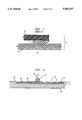
- FIG. 1 shows a portion of a prior art Multi-Chip Module (MCM) 10 comprised of at least one semiconductor chip 12 bonded to a substrate 14 (e.g., a silicon wafer).
- MCM 10 typically further includes a package (not shown) for surrounding the chip 12 and the substrate 14.
- the combination of the chip 12 and the substrate 14 forms a subassembly 16 referred to in the art as a tile.
- the tile 16 is fabricated by bonding the chip 12 to the substrate 14 via a volume of solder 17 that electrically and mechanically bonds each solder-wettable bonding pad 18 on each chip to a corresponding solder-wettable bonding site 20 on the substrate.
- Each bonding pad 18 and each bond site 20 comprises a metallized area fabricated from an appropriate solder-wettable metallization. While the chip 12 and the substrate 14 are shown with a single bonding pad 16 and single bonding site 18, respectively, typically, the chip and substrate have multiple bonding pads and bonding sites, respectively. Although not shown, each bonding pad 16 of the chip 12 may be provided with a volume of solder by the previously described evaporative process during the manufacture of the chip.
- each chip 12 is usually tested prior to solder-bonding to the substrate 14, it is nonetheless possible for a tile 16 to contain one or more defective chips. Depending on the fabrication cost of the tile, 16, it may be advantageous to repair the tile by unsoldering and removing each defective chip 12 and soldering a good chip in its place. In practice, when a defective chip 12 is removed, much of the volume of solder 17 that had bonded the chip to the substrate is also removed. Thus, there is usually an insufficient volume of solder 17 to reliably bond a "bare" replacement chip 12 (i.e., a chip having no solder on its bonding pads 20).
- the first step in the method of the invention is to screen print solder paste 22 onto a first, non-wettable surface 24 of a substrate 26, such as a silicon wafer.
- a substrate 26 such as a silicon wafer.
- the exact nature of the substrate 26 is not critical to the method of the invention except that the substrate must be capable of withstanding temperatures in excess of the reflow temperature of the paste 22. Also, it is required that the major surface 24 of the substrate be non-wettable, that is, the surface must not bond to solder. However, the substrate surface 24 must be able to be printed with solder paste.
- a silicon wafer having an un-metallized, mirrored surface has been found to be suitable for practicing the invention.
- a silicon wafer having a metallized major surface can be rendered suitable by providing a layer of KAPTON material over the metallization to provide a surface that is non-wettable, yet printable with solder paste.
- the solder paste printing operation is carried out by first securing the substrate 26 to a pallet 28 to temporarily immobilize the substrate.
- a stencil 30 is placed over the substrate in face-to-face relationship with the substrate surface 24.
- the stencil 30 typically comprises a thin sheet of metal (e.g. brass or stainless steel) having a plurality of openings 32 arranged in patterns, each corresponding to the pattern of bonding pads 18 (see FIG. 1) on a replacement chip (not shown).
- the solder paste 22 is deposited onto the stencil 30 and then a squeegee blade 34 is moved across the stencil to force the paste into the stencil openings 32 and onto the substrate surface 24. In this way, at least one solder paste pattern 36 is printed onto the surface 24.
- solder paste pattern 36 is printed, then the stencil 30 of FIG. 2 is removed. Thereafter, a bare chip 12', that is, a chip having little if any solder on its solder-wettable bonding pads 18, is placed on the substrate surface 24 such that each bonding pad on the chip contacts a portion of the solder paste pattern 36. After placement of each chip 12', the solder paste in the pattern 36 is reflowed. During reflow, the solder paste becomes molten solder that wets each pad 18 on the chip 12' and metallurgically bonds thereto, forming a solder bump 38 shown in FIG. 4.
- each now-bumped chip 12' is then removed from the substrate.
- solder-bumping each chip 12' in the manner described is that the bumping process can be carried out with the same stencil, wafer pallet, chips, chip placement program and automated placement equipment (not shown) that are normally used to fabricate the tiles 16 of FIG. 1.
- the overall cost of bumping each chip 12' will be far less than if each type of chip were bumped by the conventional process of evaporation onto the chip wafer (not shown).
- the method of the invention to used to bump individual bare chips 12 for repair purposes, the process may indeed be sufficiently economical to bump chips for production purposes as well.
Abstract
Description
Claims (4)
Priority Applications (2)
| Application Number | Priority Date | Filing Date | Title |
|---|---|---|---|
| US08/333,168 US5505367A (en) | 1994-11-02 | 1994-11-02 | Method for bumping silicon devices |
| JP7308530A JPH08213413A (en) | 1994-11-02 | 1995-11-02 | Soldering method of silicon element |
Applications Claiming Priority (1)
| Application Number | Priority Date | Filing Date | Title |
|---|---|---|---|
| US08/333,168 US5505367A (en) | 1994-11-02 | 1994-11-02 | Method for bumping silicon devices |
Publications (1)
| Publication Number | Publication Date |
|---|---|
| US5505367A true US5505367A (en) | 1996-04-09 |
Family
ID=23301613
Family Applications (1)
| Application Number | Title | Priority Date | Filing Date |
|---|---|---|---|
| US08/333,168 Expired - Lifetime US5505367A (en) | 1994-11-02 | 1994-11-02 | Method for bumping silicon devices |
Country Status (2)
| Country | Link |
|---|---|
| US (1) | US5505367A (en) |
| JP (1) | JPH08213413A (en) |
Cited By (8)
| Publication number | Priority date | Publication date | Assignee | Title |
|---|---|---|---|---|
| US5586715A (en) * | 1994-08-08 | 1996-12-24 | Hewlett-Packard Company | Method of making solder balls by contained paste deposition |
| DE19729587A1 (en) * | 1997-07-10 | 1999-01-14 | Siemens Ag | Solder application onto circuit board contact pads |
| US6099935A (en) * | 1995-12-15 | 2000-08-08 | International Business Machines Corporation | Apparatus for providing solder interconnections to semiconductor and electronic packaging devices |
| US6137063A (en) * | 1998-02-27 | 2000-10-24 | Micron Technology, Inc. | Electrical interconnections |
| US6158650A (en) * | 1997-07-09 | 2000-12-12 | Mask Technology, Inc. | Process for fine and coarse pitch solder deposits on printed circuit boards |
| US6189772B1 (en) * | 1998-08-31 | 2001-02-20 | Micron Technology, Inc. | Method of forming a solder ball |
| US6245594B1 (en) | 1997-08-05 | 2001-06-12 | Micron Technology, Inc. | Methods for forming conductive micro-bumps and recessed contacts for flip-chip technology and method of flip-chip assembly |
| US6637641B1 (en) * | 2002-05-06 | 2003-10-28 | Emc Corporation | Systems and methods for manufacturing a circuit board |
Families Citing this family (1)
| Publication number | Priority date | Publication date | Assignee | Title |
|---|---|---|---|---|
| FR2872072B1 (en) * | 2004-06-24 | 2006-09-29 | Snecma Propulsion Solide Sa | METHOD OF BRAZING PARTS OF SILICURE THERMOSTRUCTURAL COMPOSITE MATERIAL |
Citations (4)
| Publication number | Priority date | Publication date | Assignee | Title |
|---|---|---|---|---|
| JPH01199494A (en) * | 1988-02-04 | 1989-08-10 | Fujitsu Ltd | Formation of solder bump |
| US4892245A (en) * | 1988-11-21 | 1990-01-09 | Honeywell Inc. | Controlled compression furnace bonding |
| US5284287A (en) * | 1992-08-31 | 1994-02-08 | Motorola, Inc. | Method for attaching conductive balls to a substrate |
| US5323947A (en) * | 1993-05-03 | 1994-06-28 | Motorola, Inc. | Method and apparatus for use in forming pre-positioned solder bumps on a pad arrangement |
-
1994
- 1994-11-02 US US08/333,168 patent/US5505367A/en not_active Expired - Lifetime
-
1995
- 1995-11-02 JP JP7308530A patent/JPH08213413A/en active Pending
Patent Citations (4)
| Publication number | Priority date | Publication date | Assignee | Title |
|---|---|---|---|---|
| JPH01199494A (en) * | 1988-02-04 | 1989-08-10 | Fujitsu Ltd | Formation of solder bump |
| US4892245A (en) * | 1988-11-21 | 1990-01-09 | Honeywell Inc. | Controlled compression furnace bonding |
| US5284287A (en) * | 1992-08-31 | 1994-02-08 | Motorola, Inc. | Method for attaching conductive balls to a substrate |
| US5323947A (en) * | 1993-05-03 | 1994-06-28 | Motorola, Inc. | Method and apparatus for use in forming pre-positioned solder bumps on a pad arrangement |
Non-Patent Citations (4)
| Title |
|---|
| "Magnetic Stencil Paste Screening Method," Research Disclosure, Jun. 1991, No. 326, Disclosure No. 32645. |
| Magnetic Stencil Paste Screening Method, Research Disclosure, Jun. 1991, No. 326, Disclosure No. 32645. * |
| R. R. Tummala and E. J. Rymaszewski, Eds., Microelectronics Packaging Handbook, Van Nostrand Reinhold, 1989, Ch. 6, pp. 361 447. * |
| R. R. Tummala and E. J. Rymaszewski, Eds., Microelectronics Packaging Handbook, Van Nostrand Reinhold, 1989, Ch. 6, pp. 361-447. |
Cited By (12)
| Publication number | Priority date | Publication date | Assignee | Title |
|---|---|---|---|---|
| US5586715A (en) * | 1994-08-08 | 1996-12-24 | Hewlett-Packard Company | Method of making solder balls by contained paste deposition |
| US6099935A (en) * | 1995-12-15 | 2000-08-08 | International Business Machines Corporation | Apparatus for providing solder interconnections to semiconductor and electronic packaging devices |
| US6158650A (en) * | 1997-07-09 | 2000-12-12 | Mask Technology, Inc. | Process for fine and coarse pitch solder deposits on printed circuit boards |
| DE19729587A1 (en) * | 1997-07-10 | 1999-01-14 | Siemens Ag | Solder application onto circuit board contact pads |
| US6245594B1 (en) | 1997-08-05 | 2001-06-12 | Micron Technology, Inc. | Methods for forming conductive micro-bumps and recessed contacts for flip-chip technology and method of flip-chip assembly |
| US6137063A (en) * | 1998-02-27 | 2000-10-24 | Micron Technology, Inc. | Electrical interconnections |
| US6355504B1 (en) | 1998-02-27 | 2002-03-12 | Micron Technology, Inc. | Electrical interconnections, methods of conducting electricity, and methods of reducing horizontal conductivity within an anisotropic conductive adhesive |
| US6365842B1 (en) | 1998-02-27 | 2002-04-02 | Micron Technology, Inc. | Electrical circuits, circuits, and electrical couplings |
| US6579744B1 (en) | 1998-02-27 | 2003-06-17 | Micron Technology, Inc. | Electrical interconnections, methods of conducting electricity, and methods of reducing horizontal conductivity within an anisotropic conductive adhesive |
| US6189772B1 (en) * | 1998-08-31 | 2001-02-20 | Micron Technology, Inc. | Method of forming a solder ball |
| US6386436B2 (en) * | 1998-08-31 | 2002-05-14 | Micron Technology, Inc. | Method of forming a solder ball |
| US6637641B1 (en) * | 2002-05-06 | 2003-10-28 | Emc Corporation | Systems and methods for manufacturing a circuit board |
Also Published As
| Publication number | Publication date |
|---|---|
| JPH08213413A (en) | 1996-08-20 |
Similar Documents
| Publication | Publication Date | Title |
|---|---|---|
| US5860585A (en) | Substrate for transferring bumps and method of use | |
| US5564617A (en) | Method and apparatus for assembling multichip modules | |
| KR100257420B1 (en) | Systems interconnected by bumps of joining material | |
| US5873512A (en) | Application of low temperature metallurgical paste to form a bond structure to attach an electronic component to a carrier | |
| US6723629B2 (en) | Method and apparatus for attaching solder members to a substrate | |
| US5879761A (en) | Method for forming electrically conductive polymer interconnects on electrical substrates | |
| US6454159B1 (en) | Method for forming electrical connecting structure | |
| US5646068A (en) | Solder bump transfer for microelectronics packaging and assembly | |
| JPH10209625A (en) | Method and apparatus for forming solder on board | |
| US6153503A (en) | Continuous process for producing solder bumps on electrodes of semiconductor chips | |
| US6808958B2 (en) | Methods of bonding microelectronic elements | |
| US5505367A (en) | Method for bumping silicon devices | |
| EP0403631B1 (en) | Method of making high density solder bumps and a substrate socket for high density solder bumps | |
| US6239013B1 (en) | Method for transferring particles from an adhesive sheet to a substrate | |
| US7353983B2 (en) | Vertical removal of excess solder from a circuit substrate | |
| US6303407B1 (en) | Method for the transfer of flux coated particles to a substrate | |
| US20040080033A1 (en) | Flip chip assembly and method for producing the same | |
| AU653945B2 (en) | Attaching integrated circuits to circuit boards | |
| US20030189245A1 (en) | Flip chip assembly and method for producing the same | |
| US6574861B1 (en) | System and method for solder ball rework | |
| Puttlitz et al. | Solder transfer technique for flip-chip and electronic assembly applications | |
| KR100221654B1 (en) | Method for manufacturing metal bump used screen printing | |
| EP0949668A1 (en) | Method for forming bump and semiconductor device | |
| Hotchkiss et al. | Tacky Dots/sup TM/transfer of solder spheres for flip chip and electronic package applications | |
| JPH0226030A (en) | Formation of bump electrode |
Legal Events
| Date | Code | Title | Description |
|---|---|---|---|
| AS | Assignment |
Owner name: AMERICAN TELEPHONE AND TELEGRAPH, NEW YORK Free format text: ASSIGNMENT OF ASSIGNORS INTEREST;ASSIGNORS:DEGANI, YINON;DUDDERAR, THOMAS D.;SPADAFORA, JOHN G.;REEL/FRAME:007223/0304 Effective date: 19941028 |
|
| AS | Assignment |
Owner name: AT&T CORP., NEW YORK Free format text: ASSIGNMENT OF ASSIGNORS INTEREST;ASSIGNOR:AMERICAN TELELPHONE AND TELEGRAPH COMPANY;REEL/FRAME:007527/0274 Effective date: 19940420 Owner name: AT&T IPM CORP., FLORIDA Free format text: ASSIGNMENT OF ASSIGNORS INTEREST;ASSIGNOR:AT&T CORP.;REEL/FRAME:007528/0038 Effective date: 19950523 |
|
| STCF | Information on status: patent grant |
Free format text: PATENTED CASE |
|
| FEPP | Fee payment procedure |
Free format text: PAYOR NUMBER ASSIGNED (ORIGINAL EVENT CODE: ASPN); ENTITY STATUS OF PATENT OWNER: LARGE ENTITY |
|
| FPAY | Fee payment |
Year of fee payment: 4 |
|
| AS | Assignment |
Owner name: SILICON VALLEY BANK, CALIFORNIA Free format text: SECURITY AGREEMENT;ASSIGNOR:SYCHIP, INC.;REEL/FRAME:013305/0798 Effective date: 20020920 |
|
| FPAY | Fee payment |
Year of fee payment: 8 |
|
| SULP | Surcharge for late payment |
Year of fee payment: 7 |
|
| REMI | Maintenance fee reminder mailed | ||
| AS | Assignment |
Owner name: SYCHIP, INC., TEXAS Free format text: RELEASE BY SECURED PARTY;ASSIGNOR:SILICON VALLEY BANK;REEL/FRAME:016547/0870 Effective date: 20050415 |
|
| AS | Assignment |
Owner name: LUCENT TECHNOLOGIES INC., NEW JERSEY Free format text: ASSIGNMENT OF ASSIGNORS INTEREST;ASSIGNOR:AT&T CORP.;REEL/FRAME:017811/0368 Effective date: 19960329 Owner name: AGERE SYSTEMS INC., PENNSYLVANIA Free format text: ASSIGNMENT OF ASSIGNORS INTEREST;ASSIGNOR:LUCENT TECHNOLOGIES INC.;REEL/FRAME:017811/0383 Effective date: 20010130 |
|
| FPAY | Fee payment |
Year of fee payment: 12 |
|
| AS | Assignment |
Owner name: DEUTSCHE BANK AG NEW YORK BRANCH, AS COLLATERAL AG Free format text: PATENT SECURITY AGREEMENT;ASSIGNORS:LSI CORPORATION;AGERE SYSTEMS LLC;REEL/FRAME:032856/0031 Effective date: 20140506 |
|
| AS | Assignment |
Owner name: AVAGO TECHNOLOGIES GENERAL IP (SINGAPORE) PTE. LTD Free format text: ASSIGNMENT OF ASSIGNORS INTEREST;ASSIGNOR:AGERE SYSTEMS LLC;REEL/FRAME:035365/0634 Effective date: 20140804 |
|
| AS | Assignment |
Owner name: AGERE SYSTEMS LLC, PENNSYLVANIA Free format text: TERMINATION AND RELEASE OF SECURITY INTEREST IN PATENT RIGHTS (RELEASES RF 032856-0031);ASSIGNOR:DEUTSCHE BANK AG NEW YORK BRANCH, AS COLLATERAL AGENT;REEL/FRAME:037684/0039 Effective date: 20160201 Owner name: LSI CORPORATION, CALIFORNIA Free format text: TERMINATION AND RELEASE OF SECURITY INTEREST IN PATENT RIGHTS (RELEASES RF 032856-0031);ASSIGNOR:DEUTSCHE BANK AG NEW YORK BRANCH, AS COLLATERAL AGENT;REEL/FRAME:037684/0039 Effective date: 20160201 |
|
| AS | Assignment |
Owner name: BELL SEMICONDUCTOR, LLC, ILLINOIS Free format text: ASSIGNMENT OF ASSIGNORS INTEREST;ASSIGNORS:AVAGO TECHNOLOGIES GENERAL IP (SINGAPORE) PTE. LTD.;BROADCOM CORPORATION;REEL/FRAME:044886/0766 Effective date: 20171208 |
|
| AS | Assignment |
Owner name: CORTLAND CAPITAL MARKET SERVICES LLC, AS COLLATERA Free format text: SECURITY INTEREST;ASSIGNORS:HILCO PATENT ACQUISITION 56, LLC;BELL SEMICONDUCTOR, LLC;BELL NORTHERN RESEARCH, LLC;REEL/FRAME:045216/0020 Effective date: 20180124 |
|
| AS | Assignment |
Owner name: BELL NORTHERN RESEARCH, LLC, ILLINOIS Free format text: RELEASE BY SECURED PARTY;ASSIGNOR:CORTLAND CAPITAL MARKET SERVICES LLC;REEL/FRAME:059723/0382 Effective date: 20220401 Owner name: BELL SEMICONDUCTOR, LLC, ILLINOIS Free format text: RELEASE BY SECURED PARTY;ASSIGNOR:CORTLAND CAPITAL MARKET SERVICES LLC;REEL/FRAME:059723/0382 Effective date: 20220401 Owner name: HILCO PATENT ACQUISITION 56, LLC, ILLINOIS Free format text: RELEASE BY SECURED PARTY;ASSIGNOR:CORTLAND CAPITAL MARKET SERVICES LLC;REEL/FRAME:059723/0382 Effective date: 20220401 |