US5489919A - Driving method of driving a liquid crystal display element - Google Patents
Driving method of driving a liquid crystal display element Download PDFInfo
- Publication number
- US5489919A US5489919A US08/174,262 US17426293A US5489919A US 5489919 A US5489919 A US 5489919A US 17426293 A US17426293 A US 17426293A US 5489919 A US5489919 A US 5489919A
- Authority
- US
- United States
- Prior art keywords
- selection
- liquid crystal
- electrodes
- voltage
- row
- Prior art date
- Legal status (The legal status is an assumption and is not a legal conclusion. Google has not performed a legal analysis and makes no representation as to the accuracy of the status listed.)
- Expired - Lifetime
Links
Images


Classifications
-
- G—PHYSICS
- G09—EDUCATION; CRYPTOGRAPHY; DISPLAY; ADVERTISING; SEALS
- G09G—ARRANGEMENTS OR CIRCUITS FOR CONTROL OF INDICATING DEVICES USING STATIC MEANS TO PRESENT VARIABLE INFORMATION
- G09G3/00—Control arrangements or circuits, of interest only in connection with visual indicators other than cathode-ray tubes
- G09G3/20—Control arrangements or circuits, of interest only in connection with visual indicators other than cathode-ray tubes for presentation of an assembly of a number of characters, e.g. a page, by composing the assembly by combination of individual elements arranged in a matrix no fixed position being assigned to or needed to be assigned to the individual characters or partial characters
- G09G3/34—Control arrangements or circuits, of interest only in connection with visual indicators other than cathode-ray tubes for presentation of an assembly of a number of characters, e.g. a page, by composing the assembly by combination of individual elements arranged in a matrix no fixed position being assigned to or needed to be assigned to the individual characters or partial characters by control of light from an independent source
- G09G3/36—Control arrangements or circuits, of interest only in connection with visual indicators other than cathode-ray tubes for presentation of an assembly of a number of characters, e.g. a page, by composing the assembly by combination of individual elements arranged in a matrix no fixed position being assigned to or needed to be assigned to the individual characters or partial characters by control of light from an independent source using liquid crystals
- G09G3/3611—Control of matrices with row and column drivers
- G09G3/3622—Control of matrices with row and column drivers using a passive matrix
- G09G3/3625—Control of matrices with row and column drivers using a passive matrix using active addressing
-
- G—PHYSICS
- G01—MEASURING; TESTING
- G01N—INVESTIGATING OR ANALYSING MATERIALS BY DETERMINING THEIR CHEMICAL OR PHYSICAL PROPERTIES
- G01N35/00—Automatic analysis not limited to methods or materials provided for in any single one of groups G01N1/00 - G01N33/00; Handling materials therefor
- G01N35/02—Automatic analysis not limited to methods or materials provided for in any single one of groups G01N1/00 - G01N33/00; Handling materials therefor using a plurality of sample containers moved by a conveyor system past one or more treatment or analysis stations
- G01N35/026—Automatic analysis not limited to methods or materials provided for in any single one of groups G01N1/00 - G01N33/00; Handling materials therefor using a plurality of sample containers moved by a conveyor system past one or more treatment or analysis stations having blocks or racks of reaction cells or cuvettes
Definitions
- the present invention relates to a method of driving a liquid crystal display element to display fast moving images.
- liquid crystal display elements have been noted as devices which are thin, light, compact and capable of displaying a large capacity of information, in place of CRTs.
- driving methods to such liquid crystal display elements they are mainly classified into two methods wherein each picture element of a twisted nematic type liquid crystal display element is driven by a thin-film transistor which is disposed in correspondence to each of the picture elements, and a twisted nematic type or a super-twisted nematic type liquid crystal display element is driven without using a thin-film transistor (a simple matrix type).
- liquid crystal display element with a thin film transistor can be driven at a relatively high speed, there is a problem that manufacturing steps for preparing the element are complicated and manufacturing cost is high.
- manufacturing steps for the simple matrix type liquid crystal display element are relatively simple, there is a problem that it is difficult to switch a display picture at a high speed, whereby it is difficult to obtain a quick response in a display with a mouse at a terminal device when displaying video images.
- liquid crystal element having a low response time to a voltage applied to liquid crystal Such liquid crystal element is called a fast response type liquid crystal element.
- fast response type liquid crystal element In order to obtain such fast response type liquid crystal element, there are such a method of using liquid crystal having a low viscosity and such a method that the thickness of the liquid crystal layer is reduced by using liquid crystal having a large refractive index anisotropy.
- the relaxation phenomenon causes a serious problem when the number of rows multiplexed (N) is several hundreds or more and a liquid crystal display element having an average response time of about 150 msec or lower is used. In particular, it is considerable when the multiplexing is conducted to a liquid crystal display element having an average response time of about 100 msec or lower.
- the average response time of a liquid crystal display element is defined as follows.
- a light transmission degree on the application of an OFF voltage at the time when a sufficient time has passed is represented as T OFF
- a light transmission degree on the application of an ON voltage is as T ON
- the time of switching from the OFF voltage to the ON voltage is as t 1
- the time when the light transmittance degree T becomes (T ON -T OFF ) ⁇ 0.9+T OFF after the switching time is t 2
- the time of switching from the ON voltage to the OFF voltage again is as t 3
- the time when the light transmission degree T becomes (T ON -T OFF ) ⁇ 0.1+T OFF after the second switching time is as t 4
- the average response time ⁇ is expressed as follows:
- the resistance value of the electrodes is not negligible, so that there causes brightness nonuniformity in a display between a signal inputting portion of an electrode and the other portion, or there causes brightness nonuniformity in a display because of a change of V th with frequency.
- T. N. Ruckmongathan proposes a method called Improved Hybrid Addressing Technique wherein a plurality of row electrodes are selected simultaneously or as a batch to drive them (hereinafter, referred to as IHAT method) in order to reduce a driving voltage and to minimize brightness nonuniformity in a display (1988 Internal Display Research Conference).
- IHAT method Improved Hybrid Addressing Technique wherein a plurality of row electrodes are selected simultaneously or as a batch to drive them
- the driving is conducted as follows.
- a subgroup is selected as a batch.
- a line electrode pattern for the selected subgroup and a data pattern are compared for each bit by using exclusive logical sum (exclusive OR) to thereby obtain a value of the exclusive logical sum of these data.
- a mismatch number i of the two patterns is obtained from the exclusive logical sum.
- a voltage applied to the column electrodes is selected to be V i .
- the voltage applied to the column electrodes is determined independently by repeating the steps (4)-(6) in the matrix.
- a selection pattern is newly selected for the line electrodes, and a voltage applied to the column electrodes is determined through the steps (4)-(6). In the same manner as above, the voltage is applied simultaneously to another line electrodes and column electrodes during a time T R .
- a display is refreshed by repeating continuously the cycle.
- the ON/OFF ratio of root mean square (r.m.s.) value of voltage can be largest.
- the ratio of the root mean square voltage of ON and OFF is expressed by:
- the value obtainable is equal to V ON /V OFF which is obtainable by using the conventional optimized amplitude selection method. Further, the effective value of voltage at each operating portion in the matrix becomes uniform, whereby a uniform display can be obtained regardless of display patterns.
- the IHAT is effective for reducing the brightness nonuniformity of display
- the number of time intervals to complete a cycle is long and hence is not suitable for gray shades using a technique similar to frame modulation.
- a driving method of a matrix type liquid crystal display element comprising at least J ⁇ L number (J and L are respectively integers of 2 or more) of row electrodes and a plural number of column electrodes wherein,
- said J ⁇ L number of row electrodes are divided into a J number of row electrode subgroups each comprising an L number of row electrodes so that said subgroups are selected as each batch to be driven;
- voltages applied to the column electrodes are selected from an (L+1) number of voltage levels of V 0 , V 1 , . . . , V L (where V 0 ⁇ V 1 ⁇ . . . ⁇ V L ); and
- said j-th row electrode subgroup is selected by applying sequentially voltages so that the elements of a selection voltage vector which constitute a row selection voltage, as defined in the following items (a) and (b), correspond to voltages to the row electrodes constituting the j-th line electrode subgroups:
- a selection voltage vector which includes at least one of ⁇ 1 , ⁇ 2 , . . . , ⁇ k , - ⁇ 1 , - ⁇ 2 , . . . , - ⁇ k is selected, and,
- a vector ⁇ is formed by the selection voltages applied to the j-th row electrode subgroup where +V r represents 1 and -V r represents 0, and
- V i (i is an integer of any of 0 through L) given by the sum of exclusive OR of the elements corresponding to the vector ⁇ and D j is applied to the column electrodes.
- the display information of the j-th row electrode subgroup in a specified column of the plural column electrodes has a gradation of (U+1) stages (where U is a natural number of 2 or more) in place of the two-valued information;
- the selection vectors which constitute a row selection voltage comprise substantially each U number of ⁇ 1 , ⁇ 2 , . . . , ⁇ k , - ⁇ 1 , - ⁇ 2 , . . . , - ⁇ k in which the selection voltage vectors are arranged in a row, are selected, and the selected vectors having the each U number are used to display a gradation display of (U+1) stages by giving a specified ratio to the total U number of ON and OFF signs.
- FIG. 1 is a graph showing time sequential changes of electric potential of a row electrode subgroup comprising R 1 -R 4 in a case of applying the selection code shown in Table 1;
- FIGS. 2A and 2B are diagrams showing a display pattern for a liquid crystal display element
- FIG. 3 is a graph showing changes of voltages applied to column electrodes C 1 , C 2 , C 3 , C 9 with the display pattern shown in FIG. 2 in a case of applying the selection code shown in Table 1;
- FIG. 4 is graphs showing voltages applied to the electrodes R 1 -C 9 and R 2 -C 9 with the display pattern of FIG. 2 in a case of applying the selection code shown in Table 1;
- FIG. 5 is graphs showing an integrating response characteristic and a relaxation phenomenon
- FIG. 6 is a block diagram showing an example of a circuit for realizing the driving method of the present invention.
- FIG. 7 is graphs showing time sequential changes of voltages of a row electrode subgroup comprising R 1 -R 4 in a case of applying the selection code shown in Table 4;
- FIG. 8 is graphs showing time sequential changes of voltages of a row electrode subgroup comprising R 1 -R 3 in a case of applying the selection code shown in Table 6;
- FIG. 9 is graphs showing voltages applied to column electrodes C 1 , C 2 , C 3 , C 9 with the display pattern of FIG. 2 in a case of applying the selection code shown in Table 4;
- FIG. 10 is graphs showing voltages applied to the electrodes R 1 -C 9 and R 2 -C 9 with the display pattern of FIG. 2 in a case of applying the selection code shown in Table 4;
- FIG. 11 is graphs showing voltage waveforms applied to column electrodes with display patterns in a case of applying selection code shown in Table 6;
- FIG. 12 is graphs showing waveforms of the difference of electric potential between the electrode R 3 shown in FIG. 8 and an optional column electrode in cases of the entirely ON and OFF;
- FIG. 13 is a block diagram showing an example of a circuit for realizing the driving method of the present invention.
- FIG. 14 is a graph showing changes of the contrast ratios according to a conventional method and the present invention wherein the width of a selection pulse is changed;
- FIG. 15 is an another graph showing changes of the contrast ratios in accordance with conventional method and the present invention wherein the width of a selection pulse is changed.
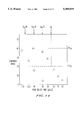
- FIG. 16 is a graph showing a relation of selection time for row electrode and the number of row electrodes.
- a plurality of row electrodes are selected as a batch in the same manner as the IHAT method.
- a group of row electrodes selected as a batch is called "a row electrode subgroup”.
- the number of row electrodes which constitute each of the row electrode subgroups is equal in order to simplify a driving circuit.
- the total number of row electrodes is not equal to a multiple number of the row electrodes which constitute row electrode subgroups, it is sometimes impossible that the number of the row electrodes which constitute all row electrode subgroups is equal.
- a fast response type liquid crystal display element it is preferable to use a fast response type liquid crystal display element.
- such fast response type liquid crystal display element can be obtained by reducing the thickness (d) of the liquid crystal layer and by using liquid crystal having a low viscosity and a large anisotropy of refractive index.
- a tolan type liquid crystal component is useful, such tolan type liquid crystal component being disclosed in, for instance, Japanese Unexamined Patent Publication No. 5631/1986.
- --X-- is --COO--, --OCO--, --CH 2 CH 2 -- of --C.tbd.C--; and R 1 and R 2 are independently a C 1 -C 10 alkyl group, a halogen atom, a cyano group or a --SCN group, provided that when R 1 and R 2 have a carbon-carbon bond, an oxygen atom may be inserted between the carbon-carbon bond of between the carbon and an adjacent ring, or a part of the carbon-carbon bonds may be substituted by --COO--, --OCO-- or --CH ⁇ CH--.
- R 1 and R 2 are independently a C 1 -C 10 alkyl group, a halogen atom, a cyano group or a --SCN group, provided that when R 1 and R 2 have a carbon-carbon bond, an oxygen atom may be inserted between the carbon-carbon bond of between the carbon and an adjacent ring, or a part of the carbon-carbon bonds may be substituted by --COO
- a difluorostilbene type liquid crystal As material having a large anisotropy of refractive index and a low viscosity, a difluorostilbene type liquid crystal is useful.
- the difluorostilbene type liquid crystal there are such liquid crystal components described in, for instance, Japanese Unexamined Patent Publication No. 96475/1989. Further, there are chemical structures shown in Chemical Formulas 2. ##STR2##
- R 1 and R 2 are independently a C 1 -C 10 alkyl group, a halogen atom, a --CN group or a --SCN group, provided that when R 1 and R 2 have a carbon-carbon bond, an oxygen atom may be inserted between the carbon-carbon bond or between the carbon and an adjacent ring, or a part of the carbon-carbon bonds may be substituted by --COO--
- the difluorostilbene type and the tolan type liquid crystal materials may be used separately or simultaneously.
- a liquid crystal composition containing 1-80% by weight of difluorostilbene, preferably 5-70% by weight, more preferably 10-60% by weight can greatly reduce the viscosity and can realize a fast response.
- voltages to be applied to line electrodes are either a voltage level of +V r or -V r (V r >0) in a selection time wherein voltages in a non-selection time are 0.
- the voltage of 0 in a non-selection time does not always mean grounding to the earth.
- a driving voltage to a liquid crystal element is determined by a voltage (a potential difference) applied between a line electrode and a column electrode. It is because a potential difference between both electrodes is not changed by changing the potential of both electrodes by the same quantity in parallel.
- the voltages applied to a specified row electrode subgroup in a selection time can be expressed by vectors with L elements which are arranged time sequentially, the vectors having, as elements, voltages applied to each row electrode.
- selection voltage matrices such matrices
- the vectors which constitute the row select voltages are called “selection voltage vectors”. Namely, if specified selection voltage matrices are determined, it is possible to select a row electrode subgroup in such a manner that the elements of the selection vectors which constitute the selection voltage matrices are made in correspondence to the voltages for each row electrodes, and the voltages corresponding to the selection voltage vectors which constitute the selection voltage matrices are sequentially applied to the row electrodes.
- List 2(a) shows a 7-row-8-column matrix formed by removing the first row from the matrix shown in List 1(c)
- List 2(b) is a 6-row-8-column matrix formed by removing the first and eighth rows from the matrix shown in List 1(c).
- the product of a matrix and a transposed matrix of the same assumes a scalar multiple of the unit matrix.
- both A and -A are selected for a selection voltage matrix, wherein A is used and then, -A is used for driving.
- selection voltage vectors basically include a 2K number of vectors which form each selection voltage matrix.
- a selection voltage to be applied to each row electrode is in a d.c. free form.
- description will be made as to a case that both A and -A are used, which is a general case.
- selection voltage matrices consisting of a 2K number of vectors wherein each of the vectors appears once in the selected voltage matrices can be selected.
- the selection voltage matrices are formed by selecting each one among the 2K number of vectors, but it is possible to add another vector composed of +V r or -V r as an element, or an arrangement of a plurality of same vectors as far as effect by the present invention is not adversely affected.
- an arrangement of selection voltage matrices including all possible conditions of electric potential in this case, the number of selection voltage vectors in the selection voltage matrices is 2 L or higher
- the selection voltage matrix includes 16 selection voltage vectors. Accordingly, the voltages corresponding to the selection voltage matrix form a row electrode selection waveform for the driving method of the present invention.
- each of the row electrode subgroups has all possible electric potential conditions, whereby brightness nonuniformity in a display can be effectively reduced.
- the number of selection pulses required for the selection of row electrodes increases in a form of exponential function, and if the pulse width is unchanged, a time required for completing a single display cycle becomes extremely long.
- the selection voltage matrices constituting the selection voltage matrices are composed substantially of ⁇ 1 , ⁇ 2 , . . . ⁇ k , - ⁇ 1 , - ⁇ 2 , . . .
- the number of the selection voltage vectors constituting the selection voltage rows is substantially 2K.
- the number of selection pulses necessary to select the row electrodes can be minimized, which is most effective for a fast response display.
- the order of an arrangement of the selection voltage vectors which constitute the selection voltage matrices is optional, and it is possible to replace the arrangement of the selection voltage vectors for each subgroup or a display information. In order to reduce the brightness nonuniformity of display in actual driving methods, it is sometimes preferred to conduct such replacement.
- selection voltage matrix (a selection code) suitable for driving fast response LCDs.
- the number of selection voltage vectors in the selection voltage matrices is 2I (I is a natural number of 2I ⁇ 2K), and the matrices consist of an I number of selection voltage vectors which form a former half portion and an I number of selection voltage vectors which form the later half portion wherein the former half and the latter half are the same in absolute value and opposite in positive and negative signs.
- a selection code when a selection code consists of a 2I number of selection patterns, and there is considered two groups: a first group of the first -Ith selection patterns and a second group of the (I+1)th-2Ith selection patterns, a selection code wherein the content of the sth selection pattern and the content of the (s+I)th selection pattern are in a negative relation should be used. Namely, a row electrode selection code should be formed so as to satisfy the relation as shown in List 3 when the sth selection pattern is expressed as W s .
- Table 1 shows an example of selection code for row electrodes which is formed from a 4 ⁇ 4 Hadamard's matrix.
- the selection code of Table 1 satisfies that the selection voltage matrices have the order of [ ⁇ 1 , ⁇ 2 , . . . ⁇ k , - ⁇ 1 , - ⁇ 2 , . . . , - ⁇ k ]. Further, selection codes shown in Tables 2 and 3 can be utilized in a case that a selection voltages (a selection pattern or patterns) are replaced for each subgroup. Numerical values in the Tables denote selection pattern numbers in Table 1. The selection patterns are applied to row electrodes time-sequentially from left to right. Table 2 shows that the selection patterns are changed after each row electrode subgroup has been selected. Table 3 shows that selection patterns are changed after every two row electrode subgroups are selected.
- Table 4 shows an example of an arrangement of the selection voltage matrices containing all possible conditions of electric potential.
- a selection code arranged in the natural binary code is shown. Further, four row electrodes are designated as a 1 , a 2 , a 3 and a 4 .
- a random code or a gray code can be utilized other than the code according to the natural binary.
- a frequency equalizing code wherein a frequency of a row electrode selection waveform is equally applied to all row electrodes in a subgroup of the row electrodes.
- a row electrode positioned apart from another row electrode on a substrate may be a row electrode in the same and single electrode subgroup.
- each of row electrodes on the substrate is as follows. Namely, when a J number of row electrode subgroups each comprising an L number of row electrodes are formed, row electrodes are divided into an L number of blocks each comprising a J number of row electrodes, and then, a row electrode is selected. In this case, the L number of row electrodes in the same subgroup are dispersely arranged on the substrate.
- an arrangement of the matrices of selection voltage vectors which constitute selection voltages include at least each U ⁇ 2K number of vectors among ⁇ 1 , ⁇ 2 , . . . , ⁇ k , - ⁇ 1 , - ⁇ 2 , . . . , - ⁇ k , is selected as the selection voltage matrices.
- the section voltage matrices consist of each 2KU number of vectors, but it is possible to add another vector as an element consisting of +V r or -V r , or to use an arrangement of a 2KU or more number of the same vectors, as far as the effect according to the present invention is not adversely affected.
- the selection voltage matrices are substantially formed of each 2KU number of the above-mentioned vectors, the number of selection pulses necessary for selecting line electrodes can be reduced, which is preferred for a high speed driving. Particularly, when the selection voltage matrices are formed of only each 2KU number of the vectors, the number of selection pulses necessary for selecting line electrodes can be minimized to perform a high speed display.
- the order of arrangement of the selection voltage vectors which constitute the selection voltage matrices is also optional.
- a random arrangement of the selection voltage vectors or the replacement of an arrangement of the selection voltage vectors for each subgroup or each display information may be used. It is often preferred to perform the above-mentioned rearrangement or replacement for driving a display element to thereby suppress unevenness of display, in the same manner as the case of using the two-valued display system.
- selection voltage vectors which constitute the selection voltage matrices can be utilized.
- the length of the non-selection time period wherein no selection voltage is applied to row electrodes is changed.
- the change can be conducted according to the method of the present invention in such a manner of dispersively applying selection pulses during the scan period.
- the voltages corresponding to the selection voltage matrices are not applied continuously to a single row electrode subgroup, but the scanning is divided into several stages in a manner that after selecting a row electrode subgroup, the next row electrode subgroup is selected.
- a predetermined number of row select vectors are applied continuously to select each row electrode subgroup before selecting the next subgroup with the same number of row select vectors.
- a cycle is completed when all the subgroups have been selected using all the vectors in the row selection matrix once.
- two selection pulses having different polarity are applied to row electrodes during scanning so as to obtain d.c.-free operation of the display. Accordingly, two selection pulses are used in a cycle.
- the number of selection pulses corresponds to the number of stages by which the selection voltage matrices are splitted. Accordingly, when the selection voltage matrices are divided into three or more, the number of the selection voltage pulses appearing during scanning period can be much more than that of the conventional method.
- the length of the non-selection time in which the selection voltages are not applied to the row electrodes can be changed according to the fast response characteristic of the liquid crystal display element.
- an increase of the number of stages divided in the selection voltage matrices reduces the non-selection time, which is effective to suppress the relaxation phenomenon in liquid crystal display.
- the most preferable way which can prevent the reduction of an average level of transmittance and the reduction of the contrast ratio is to give a single selection voltage vector in each stage.
- the total number (N) of row electrodes is selected to perform a two-valued display to form several groups each having an L number of row electrodes
- the minimum number of selection pulses to be applied to each row electrodes for a cycle is 2K ⁇ (N/L), which is substantially equal to 2N in number in the conventional method. Accordingly, if both methods have the same cycle time, the width of the selection pulses forming a selection pattern is the same between both methods.
- the feature of the method of the present invention is to increase the number of selection pulses without changing substantially the width of the selection pulses.
- FIG. 1 shows row waveforms applied to certain row electrodes in accordance with the selection code shown in Table 1 wherein R 1 -R 4 represent row electrodes, and a time interval T is a time interval between two row select pulses in a case that row electrodes having the total number N are divided into several row electrode subgroups each having an L number of row electrodes.
- FIG. 7 shows row waveforms applied to a row electrode subgroup R 1 -R 4 consisting of 4 row electrodes in accordance with the selection code shown in Table 4.
- the (L+1) number of voltage levels are used, and voltages selected from the (L+1) number of voltages in accordance with a selection pattern for a line electrode subgroup are applied to column electrodes to drive them.
- the (L+1) number of voltage levels preferably have voltages: V 0 , V 1 , . . . , V L which satisfies at least the following condition: V 0 ⁇ V 1 ⁇ . . . ⁇ V L .
- Selection of a voltage level among the above voltage levels is determined in consideration of a display information and selection voltages applied to the line electrodes. A method of determination of a suitable voltage level will be explained later.
- V i is determined as V L -i. It is possible to shift the voltages applied to the row electrodes and the column electrodes by the same amount together since there is no net change of electric potential difference between these electrodes.
- each of the voltage levels V 0 , V 1 , . . . , V L should be determined depending on the construction of a liquid crystal display element and other factors.
- FIGS. 2A & 2B show a part of a display pattern, as a form of model, of a matrix having 400 row electrodes.
- Data in a Table which is shown in the lower part of FIG. 2 correspond to the display pattern of the matrix in the upper part of FIGS. 2A & 2B wherein ON represents 1 and OFF represents 0.
- ON represents 1
- OFF represents 0.
- the data in the column electrodes are divided into several subgroups, each consisting of 4-bit data patterns.
- the display data of jth row electrode subgroup (j is an integer having 1-J) is expressed by a column vector D j having 4 number of elements (where the elements of the vector D j consist of 1 representing ON and 0 representing OFF).
- vectors ( ⁇ ) of a selection pattern of selection voltages applied to the row electrodes and vectors of a display data for the column electrodes are used and exclusive OR is applied to each elements corresponding to these vectors to thereby obtain the sum. For instance, when the selection voltages of the first subgroup of the row electrodes in FIG. 2A & 2B are expressed by a selection pattern of [1,1,1,1], voltages to be applied to the column electrode C 9 in FIGS. 2A & 2B are determined. Then, the sum of the exclusive OR operation is expressed by List 4.
- the voltage level to be applied to the electrode is expressed by V i when i is obtained.
- Table 1 is selected for the selection code for the row electrodes.
- voltages applied to the column electrodes C 1 , C 2 , C 3 and C 9 are shown in FIG. 3.
- an area indicated by R 1 -R 4 means an area showing a change of voltage in a time period in which the row electrode subgroup R 1 -R 4 is selected.
- each area R 1 -R 4 , R 5 -R 8 or R 9 -R 12 is independently depicted.
- the time axes (abscissa) are shown by eliminating selection time periods of other subgroups.
- V ON /V OFF of the effective value of voltage can be preferably maximized. Further, it is possible to adjust the levels of V r and V i so as to obtain a desired contrast ratio near the value regardless of the above-mentioned conditions.
- FIG. 4 shows a change of voltage of R 1 -C 9 (an ON state) and R 2 -C 9 (an OFF state) in FIGS. 2A & 2B in such case wherein the time axes (abscissa) is depicted by removing selection time periods for other subgroups for easy view in the same manner as FIG. 3.
- the selection codes as shown in Tables 7, 8 and 9 may be used subsequently each time a display information is changed.
- the selection code of each Table is formed by shifting the selection voltages applied to respective line electrodes.
- a basic selection code is previously determined.
- the selection code shown in Table 1 is used here.
- the selection pattern number 1 of Table 1 is applied to the first row electrode subgroup. At the same time, voltages determined from this selection pattern and display data are applied to each and every column electrode. Then, the selection pattern number 2 of Table 1 is applied to the second line electrode subgroup. At the same time, this selection pattern and voltages determined from the second selection pattern and display data are applied to every column electrodes. Then, the selection pattern number 3 of Table 1 is applied to the third row electrode subgroup. Each of the row electrodes and column electrodes are applied with the voltages in the same manner as above. The above-mentioned steps are repeatedly conducted to the subsequent row electrode subgroups until the J th subgroup.
- the selection pattern number 2 of Table 1 is applied to the first row electrode subgroup.
- the selection pattern number 3 of Table 1 is applied to the second row electrode subgroup.
- the selection patterns of Table 1 are sequentially applied to each of the row electrode subgroups until all patterns are applied, whereby a display is completed.
- the selection code of Table 8 is used. Then, in the next cycle, the selection code of Table 9 is used. After this operation, the selection code of Table 1 is used. Thus, the selection codes are sequentially used in successive cycles.
- FIG. 9 an area R 1 -R 4 represents a time period in which a row electrode subgroup R 1 -R 4 is selected.
- the area R 1 -R 4 and other areas R 5 -R 8 and R 9 -R 12 are shown independently.
- the time axes abscissa
- FIG. 9 voltages are not continuously applied. Namely, after a voltage is applied as shown in FIG. 9, voltages are applied to other row electrode subgroups. When a time necessary for applying the voltages to other subgroups has passed, another voltage is applied as shown in the figure. This is conducted in the same manner as FIG. 3.
- the time axes (abscissa) are depicted by omitting time periods for selecting other 99 subgroups which is in a non-selection state, in FIG. 7.
- the inversion code which is obtained by rearranging the above-mentioned data as a selection code, it is possible that electric potentials having the same absolute value are repeated twice in a time period for scanning a picture surface (hereinbelow, it is referred to as a frame period or a frame frequency as the reciprocal number of it).
- the frequency in the optical response of the liquid crystal is equal to the frame period, however, the frame frequency can be substantially twice when the inversion code is used as a selection code in the driving method of the present invention. Accordingly, brightness in an ON state and the contrast ratio can be increased. Further, in any display pattern, the optical response period of the liquid crystal is constant, whereby a uniform display can be obtained.
- a display can be obtained in substantially the same manner as the case of two-valued display.
- rows of vectors are selected as selection voltage matrices wherein the selection voltage vectors which constitute the selection voltage matrices are respectively composed substantially of 2KU number of the vectors among ⁇ 1 , ⁇ 2 , . . . , ⁇ k , - ⁇ 1 , - ⁇ 2 , . . . , - ⁇ k , and the selection voltage vectors are arranged in series.
- the (U+1) stage gradation display can be performed by displaying the signs of ON and OFF having a U number in total at a predetermined ratio with respect to the selection voltage vectors each composed of a U number.
- a selection code to be used is such one as shown in Table 11 which can be formed from a 4 ⁇ 4 Hadamard's matrix. In Table 11, the selection patterns are used from left to right. Further, each line of data arranged in the vertical direction corresponds to each row of row electrodes.
- the selection code may be such one as shown in Table 12.
- a gradation display can be obtained by assigning the three selection patterns to ON or OFF.
- the data having two ONs and an OFF corresponds to the second degree of gradation from the ON side.
- the data having an ON and two OFFs corresponds to the third degree of gradation from the ON side.
- the assignment of ON and OFF should be uniform to obtain good appearance.
- a row electrode subgroup consists of an L r number of row electrodes which is smaller than an L number of row electrodes which constitute another row electrode subgroup, will be described. It is assumed that a (L-L r ) number of row electrodes are added, whereby the total number of the row electrodes which constitute the regular row electrode subgroup is L.
- the row electrode subgroup is driven by applying voltages to the row electrodes and the column electrodes in the same manner as driving the regular row electrode subgroup. Specifically, when the subgroup consisting of an L r number of row electrodes is driven, it is assumed that there are a (L-L r ) number of row electrodes which correspond to the L r th, the (L r +1)th, .
- the Lth row electrodes, and display data for the assumed row electrodes are also prepared imaginarily.
- the display data may be formed of 0 or 1 in a two-valued display.
- the display data may be any degrees of gradation in a gradation display.
- the application of voltages to the column electrodes is determined as follows. Namely, with respect to a display information, the vectors D i for the display information are prepared by adding an imaginary display information. On the other hand, with respect to the selection pattern, there is used a selection pattern for the selection code applied to an L number of row electrodes which has been used to form the selection code for an L r number of row electrodes. Then, in the same manner as described before, exclusive OR operations are conducted to corresponding elements of the display information and the selection pattern to thereby obtain the sum i, whereby voltages to be applied to column electrodes are determined.
- the number of selection pulses necessary for selection and the number of voltage levels to be applied to row electrodes become larger than minimum values with respect to the row electrodes which constitute real row electrode subgroups.
- this is sometimes advantageous when the voltage level to be applied to the column electrodes are used as voltage levels applied to other devices.
- the driving method of the present invention is suitably applied to a twisted nematic liquid crystal display element, in particular to a so-called super-twisted nematic liquid crystal display element to which multiplied driving is applicable.
- the super-twisted nematic liquid crystal display element is so adapted to increase the twist angle of the liquid crystal molecules between both electrodes to cause a sharp change in the voltage - transmittance characteristic to thereby obtain a high density dot-matrix display.
- the method proposed in the article has drawbacks as follows. Since the product value ⁇ n ⁇ d of the birefrigent index ⁇ n of the liquid crystal and the thickness d of the liquid crystal layer of a liquid crystal display element is substantially in a range of 0.8 ⁇ m-1.2 ⁇ m (Japanese Unexamined Patent Publication No. 10720/1985), a display having a good contrast ratio can not be obtained unless a specified combination of hue such as yellowish green and dark blue, bluish purple and pale yellow, and so on is used, and accordingly, it is impossible to provide a monochrome display. Further, it is impossible to obtain a multi-color or a full-color display by combining a multi-color filter.
- a liquid crystal display element which comprises a liquid crystal layer including a nematic liquid crystal containing chiral material and a positive dielectric anisotropy and whose twisting angle is in a range of 160°-300°, the liquid crystal layer being interposed between a pair of substrates with transparent electrodes each having an orientation control film which are disposed in substantially parallel, and a driving means to apply a voltage across the transparent electrodes of the upper and lower substrates which hold the liquid crystal layer therebetween, wherein at least one birefrigent plate and a pair of polarization plates are disposed at an outside of the liquid crystal layer.
- a light, compact monochrome display type liquid crystal element can be obtained.
- the driving method of the present invention is suitable for such liquid crystal display element.
- FIG. 6 is an example of a circuit used to realize the driving method of the present invention.
- the circuit is adapted to display 16 degrees of gradation.
- As display data analogue signals are inputted for R, G, B colors separately.
- the signals are respectively inputted to 6-bit A/D transducers 1, 1, 1 for R, G and B to be converted into digital data.
- the converted digital data signals are corrected (so-called ⁇ correction) at a corrector 2 so as to meet the optical characteristic of liquid crystal and are transformed into data indicating gradation having a predetermined bit number which is determined by a degree of gradation, the data being received in a display memory 3.
- the data are read from the display memory 3 in a predetermined order, and are introduced into a data selector 4 where the data are assigned to an L number of subgroup memories, 5, 5, . . . , 5.
- the L number of data are inputted to gradation controlling circuits 6, 6, . . . , 6 where 15 cycles are collected together to form data of 1-bit - ON-OFF display data rows (L number), and the data are supplied to an exclusive OR/adder 7 where the exclusive OR of the L bit data and the L bit line electrode selection pattern which is supplied from a line electrode selection pattern generating circuit 11 are obtainable, and subsequently an adding operation is conducted.
- the data from the adder 7 are supplied to a column electrode driver 8.
- the line selection pattern is delayed for a time corresponding to the selection of one line at a delay circuit 12 and is supplied to a line electrode driver 13.
- Each output from the line electrode driver 13 and the column electrode driver 8 is inputted to each electrode of a liquid crystal panel 9.
- Reference numeral 10 designates a timing generating circuit.
- FIG. 13 is a diagram showing a circuit wherein a selection code including all possible states of electric potential is used.
- the N 1 number of line electrodes is divided into subgroups each having an L number of row electrodes in order to select each of the subgroups as a batch.
- a display information is displayed by transferring ⁇ bit parallel data.
- selection signals are conducted as follows.
- a clock signal is generated from a pulse generator 31.
- the pulse train is inputted to a clock terminal of an address counter 32 to form a clock signal 34.
- the clock signal 34 is inputted to a clock terminal of an N 2 stage shift register 45.
- the pulse signal is also divided in the address counter 32 to generate a load signal 35.
- the load signal is supplied to a clock terminal of a subgroup counter 36, a clock terminal of a flip-flop 37, a load terminal of an N 2 stage data latch 46, clock terminals of an L bit latch 48 and a clock terminal of N 1 /L stage shift register 49.
- the load signal 35 is divided in the subgroup counter 36 to be formed into an L/N 1 signal which is inputted to a data terminal of the flip-flop 37.
- the output of the flip-flop 37 is respectively inputted to a clock terminal of a row stage counter 39 and a data terminal of the signal N 1 /L stage shift resistor 49.
- the output of an L bit signal from the row stage counter 39 is inputted to each data terminal of the L bit data latch 48 directly or after the signal has been transformed into a gray code or any other code as necessary.
- the outputs of the L bit data latch 48 and the output of the N 1 /L stage shift register 49 are inputted to an N 1 -bit-3-level driver 50 from which an N 1 number of outputs are generated and they are inputted to row electrodes of a liquid crystal panel 51.
- ON and OFF signals corresponding to the data of a display information are prepared as follows.
- the output of address counter 32 is inputted as an RAM address signal 33 to each of the L number of the RAMs 41, 41, . . . , 41 in FIG. 13.
- the data of the display information are simultaneously read from the L number of the RAMs 41, 41, . . . , 41.
- An exclusive OR operation is conducted on the read-out data and the value of the corresponding row select pattern of the row stage counter 39, followed by summing a resulted value at an exclusive OR/adder 44 to thereby obtain g-bit data.
- the resulted g-bit data are inputted to the data terminal of the N 2 stage shift register 45 in which the data are sequentially shifted in accordance with the clock signal 34 to form complete N 2 stage data.
- the complete data are formed, they are supplied to the N 2 stage latch 46 and are memorized when the load signal 35 is inputted.
- the output of the N 2 stage latch 46 is inputted to an N 2 number of L+1 level drivers 47.
- An N 2 number of outputs of the L+1 level drivers 47 is respectively inputted to column electrodes of the liquid crystal panel 51.
- the liquid crystal display element was driven in accordance with the driving method of the present invention wherein the width of selection pulses for a selection pattern was changed. As a result, the highest contrast ratios were obtained at 25° C. as shown by triangular marks in FIG. 14.
- the liquid crystal used contained 30 wt % of difluorostilbene type liquid crystal and 43 wt % of tolan type liquid crystal, and as the characteristics of the liquid crystal as a whole, it shows 0.237 of refractive index anisotropy ⁇ n, 12.1 cSt of viscosity V and 86.7° C. of transparent point T c .
- the thickness d of the liquid crystal layer was 3.7 ⁇ m.
- the liquid crystal display element having the same structure as Example 1 was driven by using the conventional optimized amplitude selective addressing method at 1/480 duty and 1/15 bias wherein the width of selection pulses was changed.
- the highest contrast ratios were obtained as shown by circle marks in FIG. 14. From FIG. 14, it is understood that there is a great difference in contrast ratio at or near a pulse width of 20 ⁇ sec (a frame frequency of about 100 Hz), which is generally used in the optimized amplitude selective addressing method at 1/480 duty, between the present invention and the conventional method. Thus, it is understood that the relaxation phenomenon of the liquid crystal is suppressed and the contrast ratio is extremely high in the present invention.
- the liquid crystal display element was driven in accordance with the driving method of the present invention wherein the width of selection pulses for a selection pattern was changed. As a result, the highest contrast ratios were obtained at 25° C. as shown by triangular marks in FIG. 15.
- the liquid crystal used does not contain either difluorostilbene type liquid crystal or a tolan type liquid crystal, and as the characteristics of the liquid crystal as a whole, it shows 0.131 of refractive index anisotropy ⁇ n, 18.9 cSt of viscosity ⁇ , and 93.9° C. of T c .
- the thickness d of the liquid crystal was 6.7 ⁇ m.
- the liquid crystal display element having the same structure as Example 2 was driven by using the conventional optimized amplitude selective addressing method at 1/480 duty and 1/15 bias wherein the width of selection pulses was changed.
- the highest contrast ratios were obtained as shown by circle marks in FIG. 15. From FIG. 15, it is found that there is an influence by the relaxation of the liquid crystal at or near a pulse width of 20 ⁇ sec (a frame frequency of about 100 Hz), which is generally used in the voltage averaging method (1/480 duty), and the contrast ratio decreases in comparison with the driving method of the present invention.
- the pulse width can be much longer than the conventional method for the same contrast ratio.
- FIG. 16 is a graph showing a relation of the number of row voltages simultaneously selected and selection time in a case of using the same liquid crystal display elements as those in Examples 1 and 2 wherein the abscissa represents selection time T (second) for a row electrode and the ordinate represents L 50 the number of row electrodes simultaneously selected under CR 50 .
- Table 15 shows values obtained by calculation of L depending on k in cases of selection pulse widths of 12 ⁇ sec and 25 ⁇ sec.
- the liquid crystal display element was driven in accordance with the driving method of the present invention wherein the width of selection pulses for a selection pattern was 20 ⁇ sec, and the selection code of Table 13 was used. As a result, a highest contrast ratio was 80:1 at 25° C.
- the liquid crystal used did not contain a difluorostilbene type liquid crystal, but contains 61 wt % of a tolan type liquid crystal, and as the characteristics of the liquid crystal as a whole it shows 0.229 of refractive index anisotropy ⁇ n, 17.4 cSt of viscosity ⁇ and 89.2° C. of T c .
- the thickness d of the liquid crystal layer was 3.9 ⁇ m.
- the display element was driven by using the driving method of the present invention under the condition that the width of selection pulses corresponding to a selection pattern was 20 ⁇ sec, and the same selection code as in Example 3 was used. As a result, the highest contrast ratio was 75:1 at 25° C. In this case, however, the display cycle was slightly long because the number of the row electrode subgroups was larger than that of Example 3.
- the liquid crystal display element having the same structure as Example 3 was driven by using the conventional method at 1/240 duty, 1/15 bias and a selection pulse width of 20 ⁇ sec. As a result, the highest contrast ratio was 55:1.
- the highest contrast ratio was 80:1 although a time necessary to complete a display cycle was twice as much as that of Example 3.
- the liquid crystal didn't contain a difluorostilbene type liquid crystal, but contains 61 wt % of a tolan type liquid crystal, and as the characteristics of the liquid crystal as a whole, it showed 0.224 of refractive index anisotropy ⁇ n, 22.2 cSt of viscosity ⁇ and 89.4° C. of T c .
- the thickness d of the liquid crystal layer was 3.9 ⁇ m.
- IHAT selection patterns
- IHAT selection patterns
- the STN liquid crystal display element having the same structure as Example 5 was driven by using the conventional method at 1/240 duty, 1/15 bias and a selection pulse width of 12 ⁇ sec. As a result, the highest contrast ratio was 55:1.
- the STN liquid crystal display element having the same structure as Example 5 was driven by using the conventional method at 1/240 duty, 1/15 bias and a frame frequency of 90 Hz (a selection pulse width of about 46 ⁇ sec). As a result, the highest contrast ratio was 47:1.
- the highest contrast ratio was 30:1.
- the liquid crystal display element was driven in accordance with the driving method of the present invention wherein the width of selection pulses corresponding to a selection pattern was 20 ⁇ sec. As a result, the highest contrast ratio was 54:1 at 25° C.
- the liquid crystal used contained 44 wt % of a difluorostilbene type liquid crystal but didn't contain a tolan type liquid crystal. As the characteristics of the liquid crystal as a whole, it shows 0.185 of refractive index anisotropy ⁇ n, 13.8 cSt of viscosity ⁇ and 92.2° C. of T c .
- the thickness d of the liquid crystal layer was 4.7 ⁇ m.
- the liquid crystal display element having the same construction as Example 8 was driven in the same manner as Example 8 except that in the row electrode selection patterns shown in Table 12, two row electrode subgroups were selected to be applied with a selection pattern (Table 12), and thereafter, the selection pattern adjacent to the right side of the applied selection pattern was used.
- the highest contrast ratio was 54:1 which was substantially the same as that of Example 8.
- a driving method capable of reducing the brightness nonuniformity of display and providing good look.
- Example 9 In the driving method of Example 9, whenever a display cycle has finished, selection was made by shifting one by one the relation of correspondence between the row electrodes of the row electrode subgroups and the elements of the selection patterns.
- the highest contrast ratio was 54:1, which was substantially the same as Example 8.
- the brightness nonuniformity in the display was further smaller than that of Example 9, and a display having a good look was obtained.
- the STN liquid crystal display element having the same structure as Example 8 was driven by using the conventional method at 1/240 duty, 1/15 bias and with a selection pulse width of 20 ⁇ sec. As a result, the highest contrast ratio was reduced to 11:1.
- a STN liquid crystal display element which was separate from that of Example 8, having an average response speed of 45 msec (25° C.) was prepared.
- the liquid crystal used contained 44 wt % of a difluorostilbene type liquid crystal and 31 wt % of a tolan type liquid crystal, and as the characteristics of the liquid crystal as a whole, it showed 0.187 of refractive index anisotropy ⁇ n, 15.1 cSt of viscosity ⁇ and 84.9° C. of T c .
- the thickness d of the liquid crystal layer was 4.7 ⁇ m.
- the liquid crystal display element was driven by using the driving method of the present invention by determining a selection pulse width of 23 ⁇ sec and selecting a frequency equalizing code as a line electrode selection code. As a result, the highest contrast ratio was 25:1.
- the STN liquid crystal display element having the same structure as Example 11 was driven in the same manner as the driving method of Example 11 except that the selection pulse width was 12 ⁇ sec. As a result, the highest contrast ratio was 62:1.
- the STN liquid crystal display element having the same structure as Example 11 was driven by using the conventional method at 1/240 duty, 1/15 bias and a frame frequency of 90 Hz (corresponding to a pulse width of 23 ⁇ sec). As a result, the highest contrast ratio was 18:1.
- the STN liquid crystal display element having the same structure as Example 8 was used and a 4 degree gradation display of R, G and B colors was conducted by shifting the selection patterns in the same manner as Example 10.
- As the selection patterns [S, S, S, -S, -S, -S] where 1st-8th selection patterns are expressed by a matrix S, was used.
- a display having a high contrast ratio and capable of reducing unevenness could be obtained.
- Example 14 selection patterns of [S, -S, S, -S, S, -S] were used. With respect to the contrast ratio and the unevenness, substantially the same degrees as those of Example 14 could be obtained. However, slight flicker was observed.
- selection pulses are dispersed and exist in plural numbers in a single frame, whereby it is possible to reduce a change of optical state in comparison with the conventional method for a simple matrix system wherein there is only one selection pulse in a single frame.
- the driving method of the present invention is effective when a liquid crystal display element having an average response time of 200 msec or lower at a dynamic driving time, preferably 100 msec or lower, most preferably 50 msec or lower, is driven.
- the driving method of the present invention can basically utilize the features of the IHAT method, a voltage to be supplied can be reduced in comparison with the conventional method when L ⁇ 4. In this case, if the value L is increased, the voltage to be supplied is further reduced. However, when the value L is large, the number of voltage level (L+1) of a waveform to be applied to column electrodes is also increased to thereby make hardware complicated. Accordingly, at present, it is possible to determine the value L to be 3-32, more preferably 7-15.
- driver ICs for driving a liquid crystal display element can produce a 2 n (n is an integer) number of voltage levels
- a generally used driver IC can be used for driving the liquid crystal display element if the number of line electrodes for a batch selection is (2 n -1), and therefore, it is practically useful.
- the present invention since the number of selection pulses necessary to display a display information is substantially increased in comparison with the conventional method, the present invention is effective in a case of driving fast response display. Further, the present invention permits a gradation display or a colored display which have a high contrast ratio.
- the driving method of the present invention can provide uniformity in a display in comparison with the conventional method.
Abstract
Description
τ((t.sub.4 -t.sub.3)+(t.sub.2 -t.sub.1))/2
V.sub.i =V.sub.0 (M-2i)/M, and
V.sub.r =V.sub.0 N.sup.1/2 /M
V.sub.ON /V.sub.OFF =((N.sup.1/2 +1)/(N.sup.1/2 -1)).sup.1/2
W.sub.s =W.sub.s+I (s is an integer of 1-I)
TABLE 1 ______________________________________ Selection pattern No. 1 2 3 4 5 6 7 8 ______________________________________Row electrode 1 1 1 1 1 0 0 0 0Row electrode 2 1 0 1 0 0 1 0 1Row electrode 3 1 1 0 0 0 0 1 1Row electrode 4 1 0 0 1 0 1 1 0 ______________________________________
              TABLE 2
______________________________________
Subgroup No. 1
           1      2      3   4    5    6   7    8
Subgroup No. 2
           2      3      4   5    6    7   8    1
Subgroup No. 3
           3      4      5   6    7    8   1    2
Subgroup No. 4
           4      5      6   7    8    1   2    3
Subgroup No. 5
           5      6      7   8    1    2   3    4
.          .      .      .   .    .    .   .    .
.          .      .      .   .    .    .   .    .
.          .      .      .   .    .    .   .    .
______________________________________
              TABLE 3
______________________________________
Subgroup No. 1
           1      2      3   4    5    6   7    8
Subgroup No. 2
           1      2      3   4    5    6   7    8
Subgroup No. 3
           2      3      4   5    6    7   8    1
Subgroup No. 4
           2      3      4   5    6    7   8    1
Subgroup No. 5
           3      4      5   6    7    8   1    2
.          .      .      .   .    .    .   .    .
.          .      .      .   .    .    .   .    .
.          .      .      .   .    .    .   .    .
______________________________________
                                  TABLE 4
__________________________________________________________________________
No.
   1 2  3 4 5 6  7 8 9 10 11
                            12
                              13 14
                                   15
                                     16
__________________________________________________________________________
a.sub.1
   0 1  0 1 0 1  0 1 0 1  0 1 0  1 0 1
a.sub.2
   0 0  1 1 0 0  1 1 0 0  1 1 0  0 1 1
a.sub.3
   0 0  0 0 1 1  1 1 0 0  0 0 1  1 1 1
a.sub.4
   0 0  0 0 0 0  0 0 1 1  1 1 1  1 1 1
__________________________________________________________________________
                                  TABLE 5
__________________________________________________________________________
No.
   1 2  3 4 5 6  7 8 9 10 11
                            12
                              13 14
                                   15
                                     16
__________________________________________________________________________
a.sub.1
   0 1  1 1 1 0  1 1 0 0  1 0 1  0 0 0
a.sub.2
   0 0  1 1 1 1  0 1 1 0  0 1 0  1 0 0
a.sub.3
   0 0  0 1 1 1  1 0 1 1  0 0 1  0 1 0
a.sub.4
   0 0  0 0 1 1  1 1 0 1  1 0 0  1 0 1
__________________________________________________________________________
              TABLE 6
______________________________________
No.     1     2        3   4     5   6     7   8
______________________________________
a.sub.1 0     1        0   1     1   0     1   0
a.sub.2 0     0        1   1     1   1     0   0
a.sub.3 0     0        0   0     1   1     1   1
______________________________________
i=(1·1+1·1)+(0·1+0·1)+(1·1+1.multidot.1)+(0·1+0·1)=0+1+0+1=2
TABLE 7 ______________________________________ Selection pattern No. 1 2 3 4 5 6 7 8 ______________________________________Row electrode 1 1 0 1 0 0 1 0 1Row electrode 2 1 1 0 0 0 0 1 1Row electrode 3 1 0 0 1 0 1 1 0Row electrode 4 1 1 1 1 0 0 0 0 ______________________________________
TABLE 8 ______________________________________ Selection pattern No. 1 2 3 4 5 6 7 8 ______________________________________Row electrode 1 1 1 0 0 0 0 1 1Row electrode 2 1 0 0 1 0 1 1 0Row electrode 3 1 1 1 1 0 0 0 0Row electrode 4 1 0 1 0 0 1 0 1 ______________________________________
TABLE 9 ______________________________________ Selection pattern No. 1 2 3 4 5 6 7 8 ______________________________________Row electrode 1 1 0 0 1 0 1 1 0Row electrode 2 1 1 1 1 0 0 0 0Row electrode 3 1 0 1 0 0 1 0 1Row electrode 4 1 1 0 0 0 0 1 1 ______________________________________
                                  TABLE 10
__________________________________________________________________________
   d.sub.3
     0     0     0     0     1     1     1     1
   d.sub.2
     0     0     1     1     1     1     0     0
C/R
   d.sub.1
     0     1     0     1     1     0     1     0
a.sub.3 a.sub.2 a.sub.1
     i V.sub.i
           i V.sub.i
                 i V.sub.i
                       i V.sub.i
                             i V.sub.i
                                   i V.sub.i
                                         i V.sub.i
                                               i V.sub.i
__________________________________________________________________________
0 0 0
     0 -1  1 -1/3
                 1 -1/3
                       2 1/3 3 1   2 1/3 2 1/3 1 -1/3
0 0 1
     1 -1/3
           0 -1  2 1/3 1 -1/3
                             2 1/3 3 1   1 -1/3
                                               2 1/3
0 1 0
     1 -1/3
           2 1/3 0 -1  1 -1/3
                             2 1/3 1 -1/3
                                         3 1   2 1/3
0 1 1
     2 1/3 1 -1/3
                 1 -1/3
                       0 -1  1 -1/3
                                   2 1/3 2 1/3 3 1
1 1 1
     3 1   2 1/3 2 1/3 1 -1/3
                             0 -1  1 -1/3
                                         1 -1/3
                                               2 1/3
1 1 0
     2 1/3 3 1   1 -1/3
                       2 1/3 1 -1/3
                                   0 -1  2 1/3 1 -1/3
1 0 1
     2 1/3 1 -1/3
                 3 1   2 1/3 1 -13 2 1/3 0 -1  1 -1/3
1 0 0
     1 -1/3
           2 1/3 2 1/3 3 1   2 1/3 1 -1/3
                                         1 -1/3
                                               0 -1
__________________________________________________________________________
TABLE 11 ______________________________________Row 1 1 1 1 1 1 1 1 1 1 1 1 1 0 0 0 0 0 0 0 0 0 0 0 0Row 2 1 0 1 0 1 0 1 0 1 0 1 0 0 1 0 1 0 1 0 1 0 1 0 1Row 3 1 1 0 0 1 1 0 0 1 1 0 0 0 0 1 1 0 0 1 1 0 0 1 1Row 4 1 0 0 1 1 0 0 1 1 0 0 1 0 1 1 0 0 1 1 0 0 1 1 0 ______________________________________
TABLE 12 ______________________________________Row 1 1 1 1 1 0 0 0 0 1 1 1 1 0 0 0 0 1 1 1 1 0 0 0 0Row 2 1 0 1 0 0 1 0 1 1 0 1 0 0 1 0 1 1 0 1 0 0 1 0 1Row 3 1 1 0 0 0 0 1 1 1 1 0 0 0 0 1 1 1 1 0 0 0 0 1 1Row 4 1 0 0 1 0 1 1 0 1 0 0 1 0 1 1 0 1 0 0 1 0 1 1 0 ______________________________________
                                  TABLE 13
__________________________________________________________________________
1      2 3 4 5  6 7 8 9 10 11
                             12
                               13
                                 14 15
                                      16
__________________________________________________________________________
Row 1
    1  0 1 0 1  0 1 0 0 1  0 1 0 1  0 1
Row 2
    1  1 0 0 1  1 0 0 0 0  1 1 0 0  1 1
Row 3
    1  0 0 1 1  0 0 1 0 1  1 0 0 1  1 0
Row 4
    1  1 1 1 0  0 0 0 0 0  0 0 1 1  1 1
Row 5
    1  0 1 0 0  1 0 1 0 1  0 1 1 0  1 0
Row 6
    1  1 0 0 0  0 1 1 0 0  1 1 1 1  0 0
Row 7
    1  0 0 1 0  1 1 0 0 1  1 0 1 0  0 1
__________________________________________________________________________
                                  TABLE 14
__________________________________________________________________________
1      2 3 4 5  6 7 8 9 10 11
                             12
                               13
                                 14 15
                                      16
__________________________________________________________________________
Row 1
    1  1 1 1 1  1 1 1 0 0  0 0 0 0  0 0
Row 2
    1  0 1 0 1  0 1 0 0 1  0 1 0 1  0 1
Row 3
    1  1 0 0 1  1 0 0 0 0  1 1 0 0  1 1
Row 4
    1  0 0 1 1  0 0 1 0 1  1 0 0 1  1 0
Row 5
    1  1 1 1 0  0 0 0 0 0  0 0 1 1  1 1
Row 6
    1  0 1 0 0  1 0 1 0 1  0 1 1 0  1 0
Row 7
    1  1 0 0 0  0 1 1 0 0  1 1 1 1  0 0
Row 8
    1  0 0 1 0  1 1 0 0 1  1 0 1 0  0 1
__________________________________________________________________________
              TABLE 15
______________________________________
T = 12 μsec      T = 25 μsec
k →
       20     40     60   250   20   40   60    250
______________________________________
τ ↓
N = 240
200    0.3    0.6    0.9  3.6   0.6  1.2  1.8   7.5
150    0.4    0.8    1.2  4.8   0.8  1.6  2.4   10
100    0.6    1.2    1.7  7.2   1.2  2.4  3.6   15
 50    1.2    2.3    3.5  14.4  2.4  4.8  7.2   30
N = 490
200    0.6    1.2    1.8  7.4   1.2  2.1  3.7   15.3
150    0.8    1.6    2.4  9.8   1.6  3.3  4.9   20.4
100    1.2    2.4    3.5  14.7  2.4  4.9  7.4   30.6
 50    2.4    4.7    7.1  29.4  4.9  9.8  14.7  61.2
N = 768
200    0.9    1.8    2.8  11.5  1.9  3.8  5.8   24
150    1.2    2.5    3.7  15.4  2.6  5.1  7.7   32
100    1.8    3.7    5.5  23.0  3.8  7.7  11.5  48
 50    3.7    7.4    11.1 46.1  7.7  15.4 23.0  96
______________________________________
Claims (17)
L=k·N·T/τ
Priority Applications (1)
| Application Number | Priority Date | Filing Date | Title |
|---|---|---|---|
| US08/174,262 US5489919A (en) | 1991-07-08 | 1993-12-28 | Driving method of driving a liquid crystal display element |
Applications Claiming Priority (16)
| Application Number | Priority Date | Filing Date | Title |
|---|---|---|---|
| JP30-193502 | 1991-07-08 | ||
| JP03193502 | 1991-07-08 | ||
| JP03229606 | 1991-08-16 | ||
| JP12971492 | 1992-04-22 | ||
| JP4-148844 | 1992-05-15 | ||
| JP4-129714 | 1992-05-15 | ||
| JP4-148845 | 1992-05-15 | ||
| JP14884492 | 1992-05-15 | ||
| JP04148845 | 1992-05-15 | ||
| JP3-229606 | 1992-05-15 | ||
| US07/910,513 US5262881A (en) | 1991-07-08 | 1992-07-08 | Driving method of driving a liquid crystal display element |
| JP04277865A JP3119737B2 (en) | 1991-08-16 | 1992-09-22 | Driving method and driving circuit for liquid crystal display element |
| JP36051392A JP3368926B2 (en) | 1992-04-22 | 1992-12-28 | Driving method of liquid crystal display element |
| JP4-360513 | 1992-12-28 | ||
| US8352193A | 1993-06-30 | 1993-06-30 | |
| US08/174,262 US5489919A (en) | 1991-07-08 | 1993-12-28 | Driving method of driving a liquid crystal display element |
Related Parent Applications (1)
| Application Number | Title | Priority Date | Filing Date |
|---|---|---|---|
| US8352193A Continuation-In-Part | 1991-07-08 | 1993-06-30 |
Publications (1)
| Publication Number | Publication Date |
|---|---|
| US5489919A true US5489919A (en) | 1996-02-06 |
Family
ID=27577408
Family Applications (1)
| Application Number | Title | Priority Date | Filing Date |
|---|---|---|---|
| US08/174,262 Expired - Lifetime US5489919A (en) | 1991-07-08 | 1993-12-28 | Driving method of driving a liquid crystal display element |
Country Status (1)
| Country | Link |
|---|---|
| US (1) | US5489919A (en) |
Cited By (24)
| Publication number | Priority date | Publication date | Assignee | Title |
|---|---|---|---|---|
| US5594466A (en) * | 1992-10-07 | 1997-01-14 | Sharp Kabushiki Kaisha | Driving device for a display panel and a driving method of the same |
| US5682177A (en) * | 1991-07-08 | 1997-10-28 | Asahi Glass Company Ltd. | Driving method of driving a liquid crystal display element |
| US5696524A (en) * | 1994-05-18 | 1997-12-09 | Seiko Instruments Inc. | Gradative driving apparatus of liquid crystal display panel |
| US5742270A (en) * | 1996-03-06 | 1998-04-21 | Industrial Technology Research Institute | Over line scan method |
| US5767836A (en) * | 1991-04-01 | 1998-06-16 | In Focus Systems, Inc. | Gray level addressing for LCDs |
| US5774103A (en) * | 1995-09-05 | 1998-06-30 | Samsung Display Devices Co., Ltd. | Method for driving a liquid crystal display |
| US5805130A (en) * | 1994-04-27 | 1998-09-08 | Sharp Kabushiki Kaisha | Liquid crystal display device and method for driving the same |
| US5831586A (en) * | 1994-04-13 | 1998-11-03 | Asahi Glass Company Ltd. | Method of driving a picture display device |
| US5870070A (en) * | 1995-10-05 | 1999-02-09 | Sharp Kabushiki Kaisha | Liquid crystal display device and method for driving display device |
| US5929832A (en) * | 1995-03-28 | 1999-07-27 | Sharp Kabushiki Kaisha | Memory interface circuit and access method |
| US5933128A (en) * | 1995-05-17 | 1999-08-03 | Canon Kabushiki Kaisha | Chiral smectic liquid crystal apparatus and driving method therefor |
| US5953002A (en) * | 1994-08-23 | 1999-09-14 | Asahi Glass Company Ltd. | Driving method for a liquid crystal display device |
| US6025822A (en) * | 1994-04-07 | 2000-02-15 | Asahi Glass Company Ltd. | Driving device, a column electrode driving semiconductor integrated circuit and a row electrode driving semiconductor integrated circuit used for a liquid crystal display device |
| WO2000008627A1 (en) * | 1998-08-03 | 2000-02-17 | Vitaly Alexandrovich Volodin | Method and device for controlling a screen, screen and variants |
| US6031515A (en) * | 1996-09-26 | 2000-02-29 | Nec Corporation | Display driver |
| US6040826A (en) * | 1996-10-30 | 2000-03-21 | Sharp Kabushiki Kaisha | Driving circuit for driving simple matrix type display apparatus |
| US6118424A (en) * | 1995-06-05 | 2000-09-12 | Citizen Watch Co., Ltd. | Method of driving antiferroelectric liquid crystal display |
| US6130654A (en) * | 1997-02-24 | 2000-10-10 | Kabushiki Kaisha Toshiba | Driving method of a liquid crystal display device |
| US6252572B1 (en) * | 1994-11-17 | 2001-06-26 | Seiko Epson Corporation | Display device, display device drive method, and electronic instrument |
| US6297786B1 (en) * | 1997-07-15 | 2001-10-02 | Alps Electric Co., Ltd. | Liquid crystal display apparatus |
| US6396468B2 (en) * | 1997-09-26 | 2002-05-28 | Sharp Kabushiki Kaisha | Liquid crystal display device |
| US6452578B1 (en) * | 1992-03-05 | 2002-09-17 | Seiko Epson Corporation | Liquid crystal element drive method, drive circuit, and display apparatus |
| US20030030608A1 (en) * | 2001-08-09 | 2003-02-13 | Seiko Epson Corporation | Electro-optical apparatus and method of driving electro-optical material, driving circuit therefor, electronic apparatus, and display apparatus |
| US20030043099A1 (en) * | 1992-03-05 | 2003-03-06 | Akihiko Ito | Drive method, a drive circuit and a display device for liquid crystal cells |
-
1993
- 1993-12-28 US US08/174,262 patent/US5489919A/en not_active Expired - Lifetime
Non-Patent Citations (10)
| Title |
|---|
| "A New Addressing Technique for Fast Responding STN LCDs", T. Ruckmongathan, et al., Japan Display, 1992, pp. 65-68. |
| "New Addressing Technical for Multiplexed Liquid Crystal Displays", by T. N. Ruckmongathan and N. V. Madhusudana, Proceedings of the SID, vol. 24/3, 1983. |
| "Some New Addressing Techniques for RMS Responding Matrix LCD's" by T. N. Ruckmongathan, Thesis Submitted for the Degree of Doctor of Philosophy, Dept. of Electrical Communication Engineering, Indian Institute of Science, Feb. 1988. |
| "Ultimate Limited for Matrix Addressing of RMS-Responding Liquid-Crystal Displays", J. Nehring, et al.; IEEE Transations on Electron Devices, vol. ED-26, No. 5, May 1979, pp. 795-802. |
| 1988 Int l Display Research Conference, A Generalized Addressing Technique for RMS Responding Matrix LCDS , by T. N. Ruckmongathan, pp. 80 85. * |
| 1988 Int'l Display Research Conference, "A Generalized Addressing Technique for RMS Responding Matrix LCDS", by T. N. Ruckmongathan, pp. 80-85. |
| A New Addressing Technique for Fast Responding STN LCDs , T. Ruckmongathan, et al., Japan Display, 1992, pp. 65 68. * |
| New Addressing Technical for Multiplexed Liquid Crystal Displays , by T. N. Ruckmongathan and N. V. Madhusudana, Proceedings of the SID, vol. 24/3, 1983. * |
| Some New Addressing Techniques for RMS Responding Matrix LCD s by T. N. Ruckmongathan, Thesis Submitted for the Degree of Doctor of Philosophy, Dept. of Electrical Communication Engineering, Indian Institute of Science, Feb. 1988. * |
| Ultimate Limited for Matrix Addressing of RMS Responding Liquid Crystal Displays , J. Nehring, et al.; IEEE Transations on Electron Devices, vol. ED 26, No. 5, May 1979, pp. 795 802. * |
Cited By (29)
| Publication number | Priority date | Publication date | Assignee | Title |
|---|---|---|---|---|
| US5767836A (en) * | 1991-04-01 | 1998-06-16 | In Focus Systems, Inc. | Gray level addressing for LCDs |
| US5682177A (en) * | 1991-07-08 | 1997-10-28 | Asahi Glass Company Ltd. | Driving method of driving a liquid crystal display element |
| US20030043099A1 (en) * | 1992-03-05 | 2003-03-06 | Akihiko Ito | Drive method, a drive circuit and a display device for liquid crystal cells |
| US20030112210A1 (en) * | 1992-03-05 | 2003-06-19 | Akihiko Ito | Liquid crystal element drive method, drive circuit, and display apparatus |
| US6452578B1 (en) * | 1992-03-05 | 2002-09-17 | Seiko Epson Corporation | Liquid crystal element drive method, drive circuit, and display apparatus |
| US7138972B2 (en) | 1992-03-05 | 2006-11-21 | Seiko Epson Corporation | Liquid crystal element drive method, drive circuit, and display apparatus |
| US7095397B2 (en) | 1992-03-05 | 2006-08-22 | Seiko Epson Corporation | Drive method, a drive circuit and a display device for liquid crystal cells |
| US5610628A (en) * | 1992-10-07 | 1997-03-11 | Sharp Kabushiki Kaisha | Driving device for a display panel and a driving method of the same |
| US5594466A (en) * | 1992-10-07 | 1997-01-14 | Sharp Kabushiki Kaisha | Driving device for a display panel and a driving method of the same |
| US6025822A (en) * | 1994-04-07 | 2000-02-15 | Asahi Glass Company Ltd. | Driving device, a column electrode driving semiconductor integrated circuit and a row electrode driving semiconductor integrated circuit used for a liquid crystal display device |
| US5831586A (en) * | 1994-04-13 | 1998-11-03 | Asahi Glass Company Ltd. | Method of driving a picture display device |
| US5805130A (en) * | 1994-04-27 | 1998-09-08 | Sharp Kabushiki Kaisha | Liquid crystal display device and method for driving the same |
| US5696524A (en) * | 1994-05-18 | 1997-12-09 | Seiko Instruments Inc. | Gradative driving apparatus of liquid crystal display panel |
| US5953002A (en) * | 1994-08-23 | 1999-09-14 | Asahi Glass Company Ltd. | Driving method for a liquid crystal display device |
| US6252572B1 (en) * | 1994-11-17 | 2001-06-26 | Seiko Epson Corporation | Display device, display device drive method, and electronic instrument |
| US5929832A (en) * | 1995-03-28 | 1999-07-27 | Sharp Kabushiki Kaisha | Memory interface circuit and access method |
| US5933128A (en) * | 1995-05-17 | 1999-08-03 | Canon Kabushiki Kaisha | Chiral smectic liquid crystal apparatus and driving method therefor |
| US6118424A (en) * | 1995-06-05 | 2000-09-12 | Citizen Watch Co., Ltd. | Method of driving antiferroelectric liquid crystal display |
| US5774103A (en) * | 1995-09-05 | 1998-06-30 | Samsung Display Devices Co., Ltd. | Method for driving a liquid crystal display |
| US5870070A (en) * | 1995-10-05 | 1999-02-09 | Sharp Kabushiki Kaisha | Liquid crystal display device and method for driving display device |
| US5742270A (en) * | 1996-03-06 | 1998-04-21 | Industrial Technology Research Institute | Over line scan method |
| US6031515A (en) * | 1996-09-26 | 2000-02-29 | Nec Corporation | Display driver |
| US6040826A (en) * | 1996-10-30 | 2000-03-21 | Sharp Kabushiki Kaisha | Driving circuit for driving simple matrix type display apparatus |
| US6130654A (en) * | 1997-02-24 | 2000-10-10 | Kabushiki Kaisha Toshiba | Driving method of a liquid crystal display device |
| US6297786B1 (en) * | 1997-07-15 | 2001-10-02 | Alps Electric Co., Ltd. | Liquid crystal display apparatus |
| US6396468B2 (en) * | 1997-09-26 | 2002-05-28 | Sharp Kabushiki Kaisha | Liquid crystal display device |
| WO2000008627A1 (en) * | 1998-08-03 | 2000-02-17 | Vitaly Alexandrovich Volodin | Method and device for controlling a screen, screen and variants |
| US6806858B2 (en) * | 2001-08-09 | 2004-10-19 | Seiko Epson Corporation | Electro-optical apparatus and method of driving electro-optical material, driving circuit therefor, electronic apparatus, and display apparatus |
| US20030030608A1 (en) * | 2001-08-09 | 2003-02-13 | Seiko Epson Corporation | Electro-optical apparatus and method of driving electro-optical material, driving circuit therefor, electronic apparatus, and display apparatus |
Similar Documents
| Publication | Publication Date | Title |
|---|---|---|
| US5596344A (en) | Driving method of driving a liquid crystal display element | |
| US5489919A (en) | Driving method of driving a liquid crystal display element | |
| US6094243A (en) | Liquid crystal display device and method for driving the same | |
| US5953002A (en) | Driving method for a liquid crystal display device | |
| KR960003440B1 (en) | Lcd addressing system | |
| US5689280A (en) | Display apparatus and a driving method for a display apparatus | |
| US7095397B2 (en) | Drive method, a drive circuit and a display device for liquid crystal cells | |
| JP4038261B2 (en) | Light modulator | |
| US5548302A (en) | Method of driving display element and its driving device | |
| US5861869A (en) | Gray level addressing for LCDs | |
| US5508716A (en) | Plural line liquid crystal addressing method and apparatus | |
| US5754157A (en) | Method for forming column signals for a liquid crystal display apparatus | |
| KR100337419B1 (en) | A method of driving a picture display device | |
| JP3190141B2 (en) | Driving method of liquid crystal display element | |
| JP3368926B2 (en) | Driving method of liquid crystal display element | |
| JP3373226B2 (en) | Driving method of liquid crystal display element | |
| JPH0546127A (en) | Driving method for liquid crystal display element | |
| JPH0627907A (en) | Method for driving liquid crystal display element | |
| Ruckmongathan | Novel addressing methods for fast responding LCDs | |
| KR100262872B1 (en) | Driving method of liquid crystal display element | |
| JPH0627905A (en) | Driving method for liquid crystal display element | |
| JP3500382B2 (en) | Method and circuit for driving liquid crystal display element | |
| JP3576231B2 (en) | Driving method of image display device | |
| JPH0627906A (en) | Driving method for liquid crystal display element | |
| JP3681194B2 (en) | Driving method of image display device |
Legal Events
| Date | Code | Title | Description |
|---|---|---|---|
| AS | Assignment |
Owner name: ASAHI GLASS COMPANY LTD, JAPAN Free format text: ASSIGNMENT OF ASSIGNORS INTEREST;ASSIGNORS:KUWATA, TAKESHI;RUCKMONGATHAN, TEMKAR N.;NAKAGAWA, YUTAKA;AND OTHERS;REEL/FRAME:007673/0657;SIGNING DATES FROM 19940223 TO 19951009 |
|
| STCF | Information on status: patent grant |
Free format text: PATENTED CASE |
|
| FEPP | Fee payment procedure |
Free format text: PAYOR NUMBER ASSIGNED (ORIGINAL EVENT CODE: ASPN); ENTITY STATUS OF PATENT OWNER: LARGE ENTITY |
|
| FPAY | Fee payment |
Year of fee payment: 4 |
|
| AS | Assignment |
Owner name: ASAHI GLASS COMPANY LTD., JAPAN Free format text: CHANGE OF CORPORATE ADDRESS;ASSIGNOR:ASAHI GLASS COMPANY LTD.;REEL/FRAME:010557/0067 Effective date: 19991213 |
|
| FPAY | Fee payment |
Year of fee payment: 8 |
|
| FPAY | Fee payment |
Year of fee payment: 12 |
|
| AS | Assignment |
Owner name: OPTREX CORPORATION, JAPAN Free format text: ASSIGNMENT OF ASSIGNORS INTEREST;ASSIGNOR:ASAHI GLASS COMPANY, LIMITED;REEL/FRAME:020532/0769 Effective date: 20080207 |