US5486865A - Data decoder adapted to decode data of different rates and/or encoded formats - Google Patents
Data decoder adapted to decode data of different rates and/or encoded formats Download PDFInfo
- Publication number
- US5486865A US5486865A US08/036,771 US3677193A US5486865A US 5486865 A US5486865 A US 5486865A US 3677193 A US3677193 A US 3677193A US 5486865 A US5486865 A US 5486865A
- Authority
- US
- United States
- Prior art keywords
- data
- decoder
- circuit
- control
- acquisition circuit
- Prior art date
- Legal status (The legal status is an assumption and is not a legal conclusion. Google has not performed a legal analysis and makes no representation as to the accuracy of the status listed.)
- Expired - Lifetime
Links
Images


Classifications
-
- H—ELECTRICITY
- H04—ELECTRIC COMMUNICATION TECHNIQUE
- H04N—PICTORIAL COMMUNICATION, e.g. TELEVISION
- H04N7/00—Television systems
- H04N7/025—Systems for the transmission of digital non-picture data, e.g. of text during the active part of a television frame
- H04N7/035—Circuits for the digital non-picture data signal, e.g. for slicing of the data signal, for regeneration of the data-clock signal, for error detection or correction of the data signal
- H04N7/0352—Circuits for the digital non-picture data signal, e.g. for slicing of the data signal, for regeneration of the data-clock signal, for error detection or correction of the data signal for regeneration of the clock signal
-
- H—ELECTRICITY
- H04—ELECTRIC COMMUNICATION TECHNIQUE
- H04N—PICTORIAL COMMUNICATION, e.g. TELEVISION
- H04N7/00—Television systems
- H04N7/025—Systems for the transmission of digital non-picture data, e.g. of text during the active part of a television frame
- H04N7/035—Circuits for the digital non-picture data signal, e.g. for slicing of the data signal, for regeneration of the data-clock signal, for error detection or correction of the data signal
- H04N7/0355—Circuits for the digital non-picture data signal, e.g. for slicing of the data signal, for regeneration of the data-clock signal, for error detection or correction of the data signal for discrimination of the binary level of the digital data, e.g. amplitude slicers
Definitions
- This invention relates to a data decoder for decoding data transmitted in one or more lines of a field blanking interval of a television signal.
- Such decoders are used to decode data at various data rates and having various encoding formats. Examples are teletext and video programming signals (VPS).
- VPS teletext and video programming signals
- VCR control is a new development in the use of broadcast teletext data services. It is now possible to perform two VCR control functions using information contained in broadcast transmissions. The first is the selection of one or more Programmes to be recorded. To make the process of entering the time and channel information into the VCR memory easier and error free, it is possible to programme the VCR from a teletext programme schedule page, where the relevant identification information is held. The second control function is real time switching of the VCR under the control of transmitted data. This enables the desired programme to be recorded despite schedule changes, the VCR being set to record only while the correct broadcast programme label is being transmitted by the broadcaster either as teletext data or as VPS data. Thus, the desired programme may be recorded even when broadcast early or late.
- PDC--Programme Delivery Control Such transmissions (known as PDC--Programme Delivery Control) are already being provided in the UK and Germany.
- a VCR equipped with the necessary PDC decoding circuitry is easy to use and gives reliable recording of the chosen items.
- the technical specification of the PDC system is described in: Specification of the domestic video Programme Delivery Control system (PDC), European Broadcasting Union, August 1990.
- Programme selection information is either incorporated in the displayed programme schedule page as teletext control characters or sent via the teletext extension packets 26. Both methods are based completely on the World System Teletext standard, and the data can be received and decoded using a normal teletext decoder.
- Real time switching data may either be sent via the teletext extension packet 8/30/2 or as a special Video Programming Signal (VPS) sent on a dedicated TV line.
- Teletext and VPS have different data rates (Teletext 6.9375 Mbit/s, VPS 2.5 Mbit/s) and coding schemes as set out in Table 1.
- the present invention provides a data decoder for decoding data transmitted in one or more lines of a field blanking interval of a television signal, said data decoder being capable of decoding data at one of a plurality of data rates and/or encoding formats and comprising control means having a first state which causes the decoder to attempt to detect data transmitted at a first data rate and having a first encoding format and one or more further states which cause the decoder to attempt to detect data transmitted at one or more different data rates and/or different encoding formats.
- the decoder can have its data slicing circuitry adaptable for different data rates under control of the control means and can be arranged to look for different framing codes, etc., depending on the state of the control means.
- the decoder can be used to decode PDC real time switching data in either format (VPS or teletext extension packets) in order to control the functioning of a video recorder, i.e. to record a selected broadcast when it is actually being broadcast even if this does not correspond to the scheduled time, or to switch on a television set when a broadcast begins if the television set had been set to a standby condition where the majority of the circuitry had been switched off with only the timing and real time switching decoding sections operating.
- format VPN or teletext extension packets
- the control means may be arranged to change state in response to the detection of invalid data.
- the decoder may be set initially to decode data having a given data rate and encoding format and to switch to attempting to decode data having a different data rate and/or encoding format if it fails to obtain valid data from the received transmission when in the state to which it has been set.
- the control means could be arranged to take a corresponding number of states and to cycle through those states until valid data is decoded.
- the control means may be arranged to change state only when invalid data has been detected a given number of times.
- the control means may be arranged to adopt different states only on given lines during a field blanking interval and on all other lines to adopt a given one of said states.
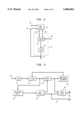
- FIG. 1 is a block schematic diagram of a data decoder according to the invention in the form of a decoder for teletext and VPS data,
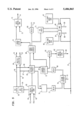
- FIG. 2 is a schematic diagram of an embodiment of a control circuit suitable for use as the control circuit of FIG. 1 showing its interaction with the acquisition circuit of FIG. 1,
- FIG. 3 is a block schematic diagram of the ADC and data slicer and clock regenerator circuit of FIG. 1,
- FIG. 4 is a schematic diagram showing an embodiment of a bit synchroniser suitable for use in the clock regenerator circuit of FIG. 3,
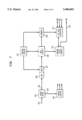
- FIG. 5 is a schematic diagram of an embodiment of an acquisition circuit for use in the decoder of FIG. 1,
- FIG. 6 is a schematic diagram of a teletext/VPS detector
- FIG. 7 is a block schematic diagram of a data decoder according to the invention for decoding real time switching signals for television sets or video recorders in the form of VPS data or teletext extension packets.
- FIG. 1 shows in block schematic form a data decoder according to the invention in the form of a decoder for teletext and VPS data.
- a data decoder according to the invention in the form of a decoder for teletext and VPS data.
- FIG. 1 it has an input 1 to which, in operation, a combined video and blanking signal CBVS is applied.
- CBVS combined video and blanking signal
- ADC analogue to digital converter
- the output of the ADC 6 feeds a data slicer and clock regenerator (DSCR) 7 which produces clock and data signals from the input signal and passes them to an acquisition circuit 8.
- the acquisition circuit 8 acquires the data from the input signal and passes it through a memory interface 9 to a memory (RAM) 10.
- the acquisition circuit 8 also receives inputs from the timing circuit 4 and from a control circuit 11 which determines whether the acquisition circuit looks for teletext or VPS data.
- the control circuit 11 receives and acts upon a signal from the acquisition circuit 8 and produces output signals which control the operation of the DSCR 7, the acquisition circuit 8 and the memory interface 9.
- the memory interface has an output which feeds a character generator 12 which produces R, G, B, and blanking signals at an output 13.
- An I2C Bus interface 14 is also connected to the memory interface 9 to enable control by an external microprocessor (not shown).
- the decoder shown in FIG. 1 is implemented as a standard teletext decoder as exemplified by that produced and sold by Philips Semiconductors under the type reference SAA 5246.
- FIG. 2 shows an embodiment of the control circuit 11 and its interaction with the acquisition circuit 8.
- the acquisition circuit 8 receives data and clock signals over line 20 from the DSCR 7 and uses these signals to decode the transmitted information in known manner.
- the acquisition circuit 8 contains the appropriate decoding means for each type of signal.
- the acquisition circuit consequently has a second input which receives a control signal from the control circuit 11 over a line 21 which signal causes the acquisition circuit to attempt to decode either teletext data or VPS data depending on the value of the signal on line 21.
- the control circuit 11 comprises a counter 22 and a latch 23.
- the counter 22 receives a first signal on a line 24 from the acquisition circuit 8 which is active when valid teletext or VPS data is decoded and causes the counter 22 to be reset to a given state.
- a second signal on a line 25 is active when valid teletext or VPS data is not decoded by the acquisition circuit 8 and enables the counter 22 to count clock pulses which are applied to an input 26.
- An output of the counter 22 is connected to a clock input of a latch 23 whose output forms the control signal which is fed to the acquisition circuit 8 over the line 21 and also to an output 27 for connection to the DSCR 7 and memory interface 9.
- clock pulses are at television frame rate and thus the counter will be incremented once each frame.
- the output of the counter will change state and clock the latch 23 causing its output to adopt a different state which is then passed over line 21 to the acquisition circuit 8, and via output 27 to the DSCR circuit 7 and memory interface 9.
- the control signal causes the acquisition circuit to attempt to decode VPS data. If it successfully decodes the input data on line 20 as valid VPS data it will cause the signal on line 24 to become active and reset the counter 22 and this state will be maintained until valid VPS data ceases to be decoded in which case the reset on line 24 will be removed and the clock enable signal on line 25 will be produced.
- the clock signal applied to input 26 is at television frame rate and hence the counter is incremented once each frame as long as valid data is not decoded by the decoder. Once valid data is obtained the counter is reset. This procedure is followed so that if a data signal is lost or corrupted by a brief interfering signal the decoder does not immediately switch over to attempt to decode the other type of data.
- the counter is set to count four clock pulses before changing the state of its output so that the temporary loss of signal will not cause the acquisition circuit to switch to decoding the other type of data.
- the number of clock pulses counted is chosen to enable a relatively fast changeover of the acquisition circuit 8 when the data type transmitted changes while allowing some margin for preventing false changeovers due to interfering signals or noise corrupting the data.
- FIG. 3 is a block schematic diagram of the ADC 6 and DSCR 7 and comprises the ADC 6 to which an input video signal is applied at input 30, a DC loop 31, an interpolator 32, an amplitude estimator 33, a zero crossing detector 34, a bit synchroniser 35, and a data latch 36.
- samples at 13.5 MHz are fed from the ADC 6 to the DC loop 31 which comprises a subtractor unit and performs a level shifting operation on the input samples.
- the amount subtracted from the input samples is made self adaptive using the output from the amplitude estimator 33.
- An interpolator 32 performs an interpolation operation on the samples from the DC Loop 31 which are sampled at 13.5 MHz. This is provided since the sampling times are not related to the data clock of either the teletext or VPS data.
- the zero crossing detector 34 detects and signals to the bit synchroniser 35 when a zero crossing has occurred and the relative phase of the zero crossing with respect to the sample clock.
- the bit synchroniser 35 feeds the interpolator 32 to enable the correct data sampling phase to be obtained and generates the teletext clock signal for application to the acquisition circuit 8 at an output 37 and to control a data latch 36 which obtains the teletext data from the interpolator 32. This teletext data is then available for application to the acquisition circuit 8 from an output 38.
- the bit synchroniser 35 is shown in greater detail in FIG. 4. It comprises a discrete time oscillator 40 to which is applied a frequency preset over a line 41.
- a phase shifter 42 provides a regenerated data clock signal at an output 43 and a phase signal for the interpolator 32 at an output 44.
- the phase shifter 42 has a further output which is connected to a first input of a phase comparator 45, to a second input of which the phase output of the zero crossing detector 34 is applied over a line 46.
- the phase comparator 45 produces an output representative of the phase error between its two inputs. This output is fed via a switch 47 to a controlled gain circuit 48 whose output feeds an integrator 49.
- the output of the integrator 49 is applied to the phase shift circuit 42 via a fixed gain stage 50.
- the switch 47 is controlled over a line 52 which carries a signal from the zero crossing detector 34 to close the switch 47 only when a zero crossing is detected so that the loop is only updated at that time.
- the data rate signal is generated by the DTO 40, the phase of which is sampled each time the zero crossing detector 34 finds a transition. As the zero crossing detector 34 also provides a measure of the phase of the signal transition, a comparison can be made (comparator 45) to give a phase error which is used to improve the phase of the locally generated clock at output 43.
- the oscillator 40 is a digital ramp generator, detection of digital overflow is sufficient to enable production of the data clock pulses. The digital ramp is supplied to the interpolator 32 to enable it to select the decimation phase used to regenerate peak data samples.
- the gain stage 48 is switchable to give an increase in the loop gain for the run-in sequence as the loop is required to find the data phase quickly from that sequence and an appropriate signal is applied over a line 51.
- the bit sychroniser 35 is as implemented in the teletext decoder type SAA 5246 mentioned hereinbefore.
- two further switches 53 and 54 are provided which are controlled by the signal produced at output 27 of the control circuit 11.
- the switch 54 when operated causes a different control word to be applied to the DTO 40 thus changing its nominal frequency and the switch 53 enables different signals to be applied to the gain stage 48 to account for the change in timing and length of the run-in sequences.
- FIG. 5 is a block diagram of the acquisition circuit 8 which comprises a serial to parallel converter 60 which takes the input data clock and data on lines 61 and 62 from outputs 37 and 38 of the DSCR7 and converts them to parallel data bytes which are fed to a teletext framing code detector 63 and a VPS start code detector 64.
- the data bytes are also fed to a resynchroniser 65 which is controlled by outputs from the detectors 63 and 64 over lines 66 and 67, respectively.
- the resynchronised data is fed to an error checking circuit 68 which performs Hamming, Parity, Biphase Decoding and Error Checking functions before feeding data via a delay 69 to an output 70 for storage via the memory interface 9 in the memory 10.
- the data is also fed to teletext page related logic 71.
- An output of the error checking circuit 68 is also fed via an error accumulator 72 to a data valid control signal generator 73 which produces a signal at an output 74 signifying whether valid data has been decoded.
- the data resynchroniser 65 produces signals for enabling a data byte counter/decoder 75 and a VPS byte counter 76.
- the VPS byte counter 76 produces an output which is fed via a delay circuit 77 to a column decoder 78 which provides a column address for the memory interface 9 over a path 79.
- the data byte counter/decoder 75 produces a first output which is fed via a delay circuit 80 to the column decoder 78, a second output which is fed via a delay 81 to a write control circuit 82 which provides a write enable signal on line 83 for application to the memory 10, and a third output which is fed to the error checking circuit 68.
- the third output will control which error checking procedures are carried out in the circuit 68 since the error protection arrangement for the transmitted data varies according to the function of the data bytes transmitted, for example, in the teletext mode some data bytes are Hamming code protected while others have simple parity bit protection.
- the teletext page relates logic circuit 71 which is entirely conventional in form and has two outputs which are fed to first inputs of respective multiplexers 84 and 85.
- the second input of multiplexer 84 receives VPS row addresses from an address generator 86 while the second input of multiplexer 85 receives VPS chapter addresses from an address generator 87.
- the multiplexers 84 and 85 provide row and chapter addresses over paths 88 and 89 respectively, to enable writing of the data to appropriate locations in the memory 10.
- the column decoder 78 and multiplexers 84 and 85 are controlled by the signal produced by the control circuit 11 and fed to the acquisition circuit 8 over the line 21 (FIG. 2). This signal is also fed to the data valid generator 73.
- the outputs of the teletext framing code detector 63 and VPS start code detector 64 are also fed over lines 91 and 92 to a VPS/teletext detector 90 which produces the signals to the control circuit 11 on lines 24 and 25.
- FIG. 6 shows an embodiment of the VPS/teletext detector 90. It comprises first and second AND gates 93 and 94 to first inputs of which the lines 91 and 92 are connected respectively.
- Line 21 carries the VPS mode signal. The signal on line 21 is applied to a second input of AND gate 94 and via an inverter 95 to a second input of AND gate 93. The data valid signal on line 74 is applied to third inputs of the AND gates 93 and 94.
- AND gate 93 will produce an output
- VPS start code is detected when the acquisition circuit is set to look for VPS signals (the signal on line 21 adopting the other state)
- AND gate 94 will produce an output.
- the outputs of AND gates 93 and 94 are fed to respective inputs of an OR gate 96 which will as a result produce an output on line 24 if either of AND gates 93 and 94 produce outputs.
- FIG. 7 shows in block schematic form a decoder for VPS data and teletext data which is arranged to acquire and store only data relevant to real time switching of video recorders and/or television sets, i.e. VPS data and teletext extension packet 8/30/2. It comprises an input 101 which is connected to an input clamp and synchronising signal separator 102 having a first output 103 connected to a timing circuit 104 and a second output 105 connected to an ADC 106. As with the arrangement described with reference to FIG. 1 the timing circuit 104 generates the appropriate clock waveforms for the other functional blocks shown.
- the output of the ADC 106 feeds a data slicer and clock regenerator circuit (DSCR) 107 which produces clock and data signals from the input data samples and feeds them to an acquisition circuit 108.
- the acquisition circuit 108 produces a first output which is fed to a memory interface and internal memory 109 to provide appropriate addressing signals and decoded data for storage in the memory.
- An I2C Bus interface 114 is provided to enable interaction between the decoder and an external microprocessor, the I2C Bus interface accessing the memory 109 and a control logic circuit 115 which indicates error free reception of VPS or packet 8/30/2 data on an output 116.
- a control circuit 111 which takes the same form as that of control circuit 11 in the embodiment of FIG. 1, produces outputs controlling the operation of the DSCR 107, acquisition circuit 108, and memory interface 109.
- FIG. 7 operates in the same way as that of FIG. 1 except that, since only real time switching data is acquired, the acquisition circuit is simpler, a small internal memory only is required since teletext page display information is not required to be stored and no character generator is required since no data is displayed.
- the functional blocks may take the same form in each embodiment.
Abstract
Description
                                  TABLE 1
__________________________________________________________________________
Difference between teletext and VPS transmissions.
Characteristic
            Teletext        VPS
__________________________________________________________________________
Data Amplitude
            0.46 V +/- 10%  0.5 V +/- 5%
Position of Start
            10.2 μs + 1 μs - 0.4 μs
                            12.5 μs +/- 1.5 μs
of Data
Data Rate   6.9375 Mbits/s  2.5 Mbit/s
Data Coding Odd Parity, 8/4 Hamming . . .
                            Biphase
Data Clock  16 bit run-in 1010 . . .
                            16 bit run-in
Synchronization             1010 . . .
Byte Sync Word
            27 hex          9951 hex
TV Lines Containing
            2-22, both fields (VBI)
                            16, first field
Data
__________________________________________________________________________
Claims (21)
Applications Claiming Priority (2)
| Application Number | Priority Date | Filing Date | Title |
|---|---|---|---|
| GB9206495 | 1992-03-25 | ||
| GB929206495A GB9206495D0 (en) | 1992-03-25 | 1992-03-25 | Receiving data signals |
Publications (1)
| Publication Number | Publication Date |
|---|---|
| US5486865A true US5486865A (en) | 1996-01-23 |
Family
ID=10712818
Family Applications (1)
| Application Number | Title | Priority Date | Filing Date |
|---|---|---|---|
| US08/036,771 Expired - Lifetime US5486865A (en) | 1992-03-25 | 1993-03-25 | Data decoder adapted to decode data of different rates and/or encoded formats |
Country Status (2)
| Country | Link |
|---|---|
| US (1) | US5486865A (en) |
| GB (1) | GB9206495D0 (en) |
Cited By (21)
| Publication number | Priority date | Publication date | Assignee | Title |
|---|---|---|---|---|
| US5781245A (en) * | 1995-02-02 | 1998-07-14 | U.S. Philips Corporation | Merging of video mosaic with teletext |
| US5812207A (en) * | 1996-12-20 | 1998-09-22 | Intel Corporation | Method and apparatus for supporting variable oversampling ratios when decoding vertical blanking interval data |
| US5812217A (en) * | 1996-06-26 | 1998-09-22 | Intel Corporation | Automatically adjusting anti-ghosting filter coefficients when the coefficients exceed particular values |
| US5812508A (en) * | 1995-12-23 | 1998-09-22 | Lg Electronics, Inc. | Digital bit signal detection circuit for reproducing optical data |
| US5838382A (en) * | 1996-06-26 | 1998-11-17 | Intel Corporation | Method and apparatus for optimizing starting point for run-in clock recovery |
| US5856852A (en) * | 1996-02-27 | 1999-01-05 | Lg Electronics Inc. | Method for providing recording-reservation data to a VCR using a TV and a VCR adapted thereto |
| WO1999021359A1 (en) * | 1997-07-17 | 1999-04-29 | Wavo Corporation | Method and system for transmitting and decoding data in a signal |
| US5926491A (en) * | 1996-06-26 | 1999-07-20 | Intel Corporation | Noise tolerant run-in clock recovery method and apparatus |
| US5953065A (en) * | 1996-06-26 | 1999-09-14 | Intel Corporation | Method and apparatus for common vertical blanking interval scan line decoding |
| US5963265A (en) * | 1996-05-03 | 1999-10-05 | Samsung Electronics Co., Ltd. | Closed-caption broadcasting and receiving method and apparatus suitable for syllable characters |
| US5973747A (en) * | 1993-12-15 | 1999-10-26 | Henley Trading Limited | Television program management system |
| US6256072B1 (en) * | 1996-05-03 | 2001-07-03 | Samsung Electronics Co., Ltd. | Closed-caption broadcasting and receiving method and apparatus thereof suitable for syllable characters |
| US6377308B1 (en) * | 1996-06-26 | 2002-04-23 | Intel Corporation | Method and apparatus for line-specific decoding of VBI scan lines |
| US6380875B2 (en) * | 1999-12-03 | 2002-04-30 | Nokia Networks Oy | Digital ramp generator with output power level controller |
| US6449016B1 (en) * | 1997-09-19 | 2002-09-10 | Infineon Technologies Ag | Separation stage for separating a signal which is transmitted in the blanking intervals of a video signal and a distortion-compensation method for such a signal |
| US6483553B1 (en) * | 1998-05-15 | 2002-11-19 | Lg Electronics Inc. | TV receiver for digital/analog combined use |
| US20070022461A1 (en) * | 2003-09-05 | 2007-01-25 | Janghwan Lee | Auxiliary information processing system |
| US20070064149A1 (en) * | 2005-09-16 | 2007-03-22 | Yi-Le Yang | Data recovery device and data recovery method for television signals |
| US7334132B1 (en) * | 2003-06-27 | 2008-02-19 | Zoran Corporation | Flexible and scalable architecture for transport processing |
| US20090234971A1 (en) * | 2008-03-14 | 2009-09-17 | Microsoft Corporation | Encoding/decoding while allowing varying message formats per message |
| US20190196008A1 (en) * | 2017-12-22 | 2019-06-27 | Samsung Electronics Co., Ltd. | Method and device to detect object |
Citations (7)
| Publication number | Priority date | Publication date | Assignee | Title |
|---|---|---|---|---|
| EP0306208A2 (en) * | 1987-09-02 | 1989-03-08 | Ing. C. Olivetti & C., S.p.A. | Method and apparatus for the transmission and/or reception of computer programs and/or data by way of teletext |
| JPS6476144A (en) * | 1987-09-18 | 1989-03-22 | Hitachi Ltd | Bus right deciding system |
| WO1992000648A1 (en) * | 1990-06-23 | 1992-01-09 | Telefunken Fernseh Und Rundfunk Gmbh | System for transmitting and decoding biphase coded data, in particular for vps |
| US5113440A (en) * | 1989-07-21 | 1992-05-12 | Oci Communcations, Inc. | Universal decoder |
| JPH0514869A (en) * | 1991-06-28 | 1993-01-22 | Sony Corp | Video signal transmission method |
| US5343300A (en) * | 1990-03-22 | 1994-08-30 | Rca Thomson Licensing Corporation | Apparatus for providing TV program information |
| EP0337336B1 (en) * | 1988-04-15 | 1994-12-14 | RCA Thomson Licensing Corporation | Applications for information transmitted in the vertical retrace interval of a television signal |
-
1992
- 1992-03-25 GB GB929206495A patent/GB9206495D0/en active Pending
-
1993
- 1993-03-25 US US08/036,771 patent/US5486865A/en not_active Expired - Lifetime
Patent Citations (7)
| Publication number | Priority date | Publication date | Assignee | Title |
|---|---|---|---|---|
| EP0306208A2 (en) * | 1987-09-02 | 1989-03-08 | Ing. C. Olivetti & C., S.p.A. | Method and apparatus for the transmission and/or reception of computer programs and/or data by way of teletext |
| JPS6476144A (en) * | 1987-09-18 | 1989-03-22 | Hitachi Ltd | Bus right deciding system |
| EP0337336B1 (en) * | 1988-04-15 | 1994-12-14 | RCA Thomson Licensing Corporation | Applications for information transmitted in the vertical retrace interval of a television signal |
| US5113440A (en) * | 1989-07-21 | 1992-05-12 | Oci Communcations, Inc. | Universal decoder |
| US5343300A (en) * | 1990-03-22 | 1994-08-30 | Rca Thomson Licensing Corporation | Apparatus for providing TV program information |
| WO1992000648A1 (en) * | 1990-06-23 | 1992-01-09 | Telefunken Fernseh Und Rundfunk Gmbh | System for transmitting and decoding biphase coded data, in particular for vps |
| JPH0514869A (en) * | 1991-06-28 | 1993-01-22 | Sony Corp | Video signal transmission method |
Non-Patent Citations (8)
| Title |
|---|
| IEEE Transactions On Consumer Electornics, vol. 38, No. 3, Aug. 1992, pp. 288 295, New Devices For VCR Control Using Teletext Services. * |
| IEEE Transactions On Consumer Electornics, vol. 38, No. 3, Aug. 1992, pp. 288-295, New Devices For VCR Control Using Teletext Services. |
| J nke, Manfred; A Multistandard Teletext Processor , IEEE Transaction on Consumer Electronics vol. 38 No. 3 Aug. 1992. * |
| James, Shirley; "New Devices for VCR Control Using Teletext Services", IEEE Transaction on Consumer Electronics vol. 38 No. 3 Aug. 92. |
| James, Shirley; New Devices for VCR Control Using Teletext Services , IEEE Transaction on Consumer Electronics vol. 38 No. 3 Aug. 92. * |
| Junke, Manfred; "A Multistandard Teletext Processor", IEEE Transaction on Consumer Electronics vol. 38 No. 3 Aug. 1992. |
| Tarrant, D. R.; "Advances in Teletext Decoder Design", IEEE Transaction of Consumer Electronics vol. 35, No. 3 Aug. 89. |
| Tarrant, D. R.; Advances in Teletext Decoder Design , IEEE Transaction of Consumer Electronics vol. 35, No. 3 Aug. 89. * |
Cited By (26)
| Publication number | Priority date | Publication date | Assignee | Title |
|---|---|---|---|---|
| US5973747A (en) * | 1993-12-15 | 1999-10-26 | Henley Trading Limited | Television program management system |
| US5781245A (en) * | 1995-02-02 | 1998-07-14 | U.S. Philips Corporation | Merging of video mosaic with teletext |
| US5812508A (en) * | 1995-12-23 | 1998-09-22 | Lg Electronics, Inc. | Digital bit signal detection circuit for reproducing optical data |
| US5856852A (en) * | 1996-02-27 | 1999-01-05 | Lg Electronics Inc. | Method for providing recording-reservation data to a VCR using a TV and a VCR adapted thereto |
| US5963265A (en) * | 1996-05-03 | 1999-10-05 | Samsung Electronics Co., Ltd. | Closed-caption broadcasting and receiving method and apparatus suitable for syllable characters |
| US6256072B1 (en) * | 1996-05-03 | 2001-07-03 | Samsung Electronics Co., Ltd. | Closed-caption broadcasting and receiving method and apparatus thereof suitable for syllable characters |
| US6377308B1 (en) * | 1996-06-26 | 2002-04-23 | Intel Corporation | Method and apparatus for line-specific decoding of VBI scan lines |
| US5838382A (en) * | 1996-06-26 | 1998-11-17 | Intel Corporation | Method and apparatus for optimizing starting point for run-in clock recovery |
| US5812217A (en) * | 1996-06-26 | 1998-09-22 | Intel Corporation | Automatically adjusting anti-ghosting filter coefficients when the coefficients exceed particular values |
| US5926491A (en) * | 1996-06-26 | 1999-07-20 | Intel Corporation | Noise tolerant run-in clock recovery method and apparatus |
| US5953065A (en) * | 1996-06-26 | 1999-09-14 | Intel Corporation | Method and apparatus for common vertical blanking interval scan line decoding |
| US5812207A (en) * | 1996-12-20 | 1998-09-22 | Intel Corporation | Method and apparatus for supporting variable oversampling ratios when decoding vertical blanking interval data |
| US6005632A (en) * | 1996-12-20 | 1999-12-21 | Intel Corporation | Method and apparatus for supporting variable sampling rates when decoding vertical blanking interval data |
| WO1999021359A1 (en) * | 1997-07-17 | 1999-04-29 | Wavo Corporation | Method and system for transmitting and decoding data in a signal |
| US6449016B1 (en) * | 1997-09-19 | 2002-09-10 | Infineon Technologies Ag | Separation stage for separating a signal which is transmitted in the blanking intervals of a video signal and a distortion-compensation method for such a signal |
| US6483553B1 (en) * | 1998-05-15 | 2002-11-19 | Lg Electronics Inc. | TV receiver for digital/analog combined use |
| US6380875B2 (en) * | 1999-12-03 | 2002-04-30 | Nokia Networks Oy | Digital ramp generator with output power level controller |
| US7334132B1 (en) * | 2003-06-27 | 2008-02-19 | Zoran Corporation | Flexible and scalable architecture for transport processing |
| US20070022461A1 (en) * | 2003-09-05 | 2007-01-25 | Janghwan Lee | Auxiliary information processing system |
| US20070064149A1 (en) * | 2005-09-16 | 2007-03-22 | Yi-Le Yang | Data recovery device and data recovery method for television signals |
| US8115868B2 (en) * | 2005-09-16 | 2012-02-14 | Realtek Semiconductor Corp. | Data recovery device and data recovery method for television signals |
| US20090234971A1 (en) * | 2008-03-14 | 2009-09-17 | Microsoft Corporation | Encoding/decoding while allowing varying message formats per message |
| US8145794B2 (en) * | 2008-03-14 | 2012-03-27 | Microsoft Corporation | Encoding/decoding while allowing varying message formats per message |
| US8812643B2 (en) | 2008-03-14 | 2014-08-19 | Microsoft Corporation | Conversion of hierarchical infoset type data to binary data |
| US20190196008A1 (en) * | 2017-12-22 | 2019-06-27 | Samsung Electronics Co., Ltd. | Method and device to detect object |
| US10908276B2 (en) * | 2017-12-22 | 2021-02-02 | Samsung Electronics Co., Ltd. | Method and device to detect object |
Also Published As
| Publication number | Publication date |
|---|---|
| GB9206495D0 (en) | 1992-05-06 |
Similar Documents
| Publication | Publication Date | Title |
|---|---|---|
| US5486865A (en) | Data decoder adapted to decode data of different rates and/or encoded formats | |
| JP5528144B2 (en) | Method for processing a received video signal representing a video program | |
| KR100375799B1 (en) | Simplified bus and interface systems used in consumer digital equipment | |
| US4745476A (en) | Television sound signal processing apparatus | |
| EP0567168B1 (en) | Data decoder | |
| KR950009455B1 (en) | Soumd decoder | |
| EP0973329B1 (en) | HDTV video frame synchronizer that provides clean digital video without variable delay | |
| US6020927A (en) | Video signal format converter | |
| US4712131A (en) | Sync apparatus for image multiplex transmission system | |
| EP0768010B1 (en) | Transport processor interface and video recorder/playback apparatus for a digital television system | |
| EP0797354B1 (en) | Recording and/or replaying teletext signals | |
| EP0220057B1 (en) | System for phase correction of a color television signal | |
| US5235425A (en) | Automatic tuning method and device thereof | |
| JPH1013796A (en) | Teletext multiplex data sampling circuit | |
| US7203557B1 (en) | Audio signal delay apparatus and method | |
| EP0141459B1 (en) | Television receiver arrangements | |
| James | New devices for VCR control using teletext services | |
| EP0592518B1 (en) | Horizontal line counter insensitive to large phase shifts of video | |
| US4535362A (en) | Method of transferring data in a television receiver | |
| GB2225519A (en) | Teletext data encoding/decoding method | |
| JP2950871B2 (en) | Character data playback method for teletext receiver | |
| JP2549673Y2 (en) | Teletext playback device | |
| KR960003878B1 (en) | Muse decoder | |
| EP0648053A2 (en) | Teletext signals receiver with a framing code position detector | |
| JPH08289261A (en) | Teletext reception circuit |
Legal Events
| Date | Code | Title | Description |
|---|---|---|---|
| AS | Assignment |
Owner name: U.S. PHILIPS CORP., NEW YORK Free format text: ASSIGNMENT OF ASSIGNORS INTEREST.;ASSIGNOR:JAMES, SHIRLEY J.;REEL/FRAME:006519/0299 Effective date: 19930316 |
|
| STPP | Information on status: patent application and granting procedure in general |
Free format text: APPLICATION UNDERGOING PREEXAM PROCESSING |
|
| FPAY | Fee payment |
Year of fee payment: 4 |
|
| FPAY | Fee payment |
Year of fee payment: 8 |
|
| AS | Assignment |
Owner name: NXP B.V., NETHERLANDS Free format text: ASSIGNMENT OF ASSIGNORS INTEREST;ASSIGNOR:U.S. PHILIPS CORPORATION;REEL/FRAME:018635/0755 Effective date: 20061127 |
|
| AS | Assignment |
Owner name: MORGAN STANLEY SENIOR FUNDING, INC., ENGLAND Free format text: SECURITY AGREEMENT;ASSIGNOR:NXP B.V.;REEL/FRAME:018806/0201 Effective date: 20061201 |
|
| FPAY | Fee payment |
Year of fee payment: 12 |
|
| AS | Assignment |
Owner name: NXP B.V.,NETHERLANDS Free format text: RELEASE BY SECURED PARTY;ASSIGNOR:MORGAN STANLEY SENIOR FUNDING, INC.;REEL/FRAME:023905/0787 Effective date: 20100208 |
|
| AS | Assignment |
Owner name: TRIDENT MICROSYSTEMS (FAR EAST) LTD.,CAYMAN ISLAND Free format text: ASSIGNMENT OF ASSIGNORS INTEREST;ASSIGNORS:TRIDENT MICROSYSTEMS (EUROPE) B.V.;NXP HOLDING 1 B.V.;REEL/FRAME:023928/0552 Effective date: 20100208 Owner name: NXP HOLDING 1 B.V.,NETHERLANDS Free format text: ASSIGNMENT OF ASSIGNORS INTEREST;ASSIGNOR:NXP;REEL/FRAME:023928/0489 Effective date: 20100207 Owner name: NXP HOLDING 1 B.V., NETHERLANDS Free format text: ASSIGNMENT OF ASSIGNORS INTEREST;ASSIGNOR:NXP;REEL/FRAME:023928/0489 Effective date: 20100207 Owner name: TRIDENT MICROSYSTEMS (FAR EAST) LTD., CAYMAN ISLAN Free format text: ASSIGNMENT OF ASSIGNORS INTEREST;ASSIGNORS:TRIDENT MICROSYSTEMS (EUROPE) B.V.;NXP HOLDING 1 B.V.;REEL/FRAME:023928/0552 Effective date: 20100208 |
|
| AS | Assignment |
Owner name: ENTROPIC COMMUNICATIONS, INC., CALIFORNIA Free format text: ASSIGNMENT OF ASSIGNORS INTEREST;ASSIGNORS:TRIDENT MICROSYSTEMS, INC.;TRIDENT MICROSYSTEMS (FAR EAST) LTD.;REEL/FRAME:028153/0440 Effective date: 20120411 |
|
| AS | Assignment |
Owner name: NXP B.V., NETHERLANDS Free format text: RELEASE BY SECURED PARTY;ASSIGNOR:MORGAN STANLEY SENIOR FUNDING, INC;REEL/FRAME:050315/0443 Effective date: 20190903 |