US5448822A - Method of making a thin film magnetic head having multi-layer coils - Google Patents
Method of making a thin film magnetic head having multi-layer coils Download PDFInfo
- Publication number
- US5448822A US5448822A US08/029,125 US2912593A US5448822A US 5448822 A US5448822 A US 5448822A US 2912593 A US2912593 A US 2912593A US 5448822 A US5448822 A US 5448822A
- Authority
- US
- United States
- Prior art keywords
- coil
- pattern
- windings
- coils
- layer
- Prior art date
- Legal status (The legal status is an assumption and is not a legal conclusion. Google has not performed a legal analysis and makes no representation as to the accuracy of the status listed.)
- Expired - Lifetime
Links
Images


Classifications
-
- G—PHYSICS
- G11—INFORMATION STORAGE
- G11B—INFORMATION STORAGE BASED ON RELATIVE MOVEMENT BETWEEN RECORD CARRIER AND TRANSDUCER
- G11B5/00—Recording by magnetisation or demagnetisation of a record carrier; Reproducing by magnetic means; Record carriers therefor
- G11B5/127—Structure or manufacture of heads, e.g. inductive
- G11B5/31—Structure or manufacture of heads, e.g. inductive using thin films
- G11B5/3163—Fabrication methods or processes specially adapted for a particular head structure, e.g. using base layers for electroplating, using functional layers for masking, using energy or particle beams for shaping the structure or modifying the properties of the basic layers
-
- G—PHYSICS
- G11—INFORMATION STORAGE
- G11B—INFORMATION STORAGE BASED ON RELATIVE MOVEMENT BETWEEN RECORD CARRIER AND TRANSDUCER
- G11B5/00—Recording by magnetisation or demagnetisation of a record carrier; Reproducing by magnetic means; Record carriers therefor
- G11B5/127—Structure or manufacture of heads, e.g. inductive
- G11B5/31—Structure or manufacture of heads, e.g. inductive using thin films
- G11B5/3109—Details
- G11B5/313—Disposition of layers
-
- H—ELECTRICITY
- H01—ELECTRIC ELEMENTS
- H01F—MAGNETS; INDUCTANCES; TRANSFORMERS; SELECTION OF MATERIALS FOR THEIR MAGNETIC PROPERTIES
- H01F41/00—Apparatus or processes specially adapted for manufacturing or assembling magnets, inductances or transformers; Apparatus or processes specially adapted for manufacturing materials characterised by their magnetic properties
- H01F41/02—Apparatus or processes specially adapted for manufacturing or assembling magnets, inductances or transformers; Apparatus or processes specially adapted for manufacturing materials characterised by their magnetic properties for manufacturing cores, coils, or magnets
- H01F41/04—Apparatus or processes specially adapted for manufacturing or assembling magnets, inductances or transformers; Apparatus or processes specially adapted for manufacturing materials characterised by their magnetic properties for manufacturing cores, coils, or magnets for manufacturing coils
- H01F41/041—Printed circuit coils
- H01F41/042—Printed circuit coils by thin film techniques
-
- Y—GENERAL TAGGING OF NEW TECHNOLOGICAL DEVELOPMENTS; GENERAL TAGGING OF CROSS-SECTIONAL TECHNOLOGIES SPANNING OVER SEVERAL SECTIONS OF THE IPC; TECHNICAL SUBJECTS COVERED BY FORMER USPC CROSS-REFERENCE ART COLLECTIONS [XRACs] AND DIGESTS
- Y10—TECHNICAL SUBJECTS COVERED BY FORMER USPC
- Y10T—TECHNICAL SUBJECTS COVERED BY FORMER US CLASSIFICATION
- Y10T29/00—Metal working
- Y10T29/49—Method of mechanical manufacture
- Y10T29/49002—Electrical device making
- Y10T29/4902—Electromagnet, transformer or inductor
- Y10T29/49021—Magnetic recording reproducing transducer [e.g., tape head, core, etc.]
- Y10T29/49032—Fabricating head structure or component thereof
- Y10T29/4906—Providing winding
- Y10T29/49062—Multilayered winding
Definitions
- Thin-film magnetic heads are used to perform both "write” and “read” operations on magnetic medias.
- a thin-film magnetic head consists of a core of ferromagnetic material, such as permalloy, with a multi-turn coil wrapped around the core.
- a magnetic flux is induced in the head during "write” operations to magnetize underlying memory storage media.
- magnetized storage media is passed by the head, inducing an electrical voltage in the coil.
- the induced level of electrical voltage is increased by the number of flux interactions between the permalloy and the coil.
- the increase in the number of flux interactions has been accomplished by adding more turns into the coil, by reducing the coil pitch, or adding more layers of coils.
- a typical thin-film inductive head needs a minimum of two layers of coils to meet the performance requirements.
- a multi-layer coil is fabricated by forming a first metallic coil on a substrate through either a plating process or a deposition and photo engraving process. A layer of photoresist is then spun onto the first coil and hard baked in a vacuum to insulate the first coil. Subsequent coil layers are formed over the first coil by repeating the same processes to obtain a multi-layer coil structure.
- the processing time to produce and insulate each coil layer is lengthy.
- the processing time further increases as the number of coil layers increase.
- An increase in the number of coil layers also increases the process complexity.
- the difficulty in manufacturing a consistent multi-layer coil pattern results in low yields and higher manufacturing costs.
- the present invention relates to a method of forming a thin-film magnetic head having a multi-layer coil and the resultant magnetic head so formed.
- the magnetic head is made by first forming an insulative resist layer, such as photoresist, over a substrate. Selected areas of the upper surface of the resist layer are exposed to light, which renders predetermined areas of the resist layer more soluble than other areas. The solubility varies across the thickness of the resist layer. The more soluble areas of the resist layer are then dissolved to produce a raised, substantially convoluted pattern of resist at predetermined locations where the windings for the top coil are to be formed. Spaces are left between the raised portions. The sidewalls of the pattern have a negative slope because of the varying solubility with thickness. In other words, the resist pattern varies in width from larger to smaller from the upper surface of the resist layer to the lower surface.
- coil metallization is deposited over the pattern such that a bottom coil is formed on the lower convoluted surface in the space between the resist pattern and a top coil is formed on the upper convoluted surface of the resist pattern. Because of the negative slope of the sidewalls, a void occurs in which no metallization is formed, between the upper and lower coils.
- a low viscosity resist insulator is deposited to fill in the voids between the bottom coil and the sidewalls of the pattern.
- an insulative layer is deposited over the metallization which makes up the top and bottom coils.
- top and bottom coils wind in the same direction and are wrapped about a core of ferromagnetic material.
- the top coil windings are aligned between the bottom coil windings.
- a jumper wire is used to electrically connect the top and bottom coils in electrical series.
- FIG. 1 is a plan view of the present invention thin film magnetic head having multi-layer coils.
- FIG. 2 is a cross-sectional view of the present invention thin film magnetic head taken along 2--2.
- FIG. 3 is a cross-sectional view of the present invention thin film magnetic head taken along 3--3.
- FIG. 4 schematically depicts the top and bottom coils wrapped about the magnet.
- FIG. 5a is a cross-sectional view of a layer of photoresist deposited on the substrate and masked for exposure to light.
- FIG. 5b is a cross-sectional view of the pattern of photoresist on the substrate.
- FIG. 5c is a cross-sectional view depicting top and bottom coils deposited on the photoresist pattern and the substrate.
- FIG. 5d is a cross-sectional view depicting the top and bottom coils covered with low viscosity photoresist.
- FIG. 5e is a cross-sectional view showing an insulating layer of photoresist covering the top and bottom coils.
- FIG. 6 is a cross-sectional view depicting an alternate photoresist pattern having a stepped sidewall.
- Head 10 is formed of two coils C1 and C2 having spiral or convoluted windings 56 and 58 respectively.
- the windings 58 of coil C2 are disposed above and between the windings 56 of Coil C1.
- An insulating photoresist layer 24 separates and covers coils C1 and C2 to electrically insulate the coils from each other.
- Coils Cl and C2 are wound in the same direction so that the magnetic fields of those coils do not cancel each other out.
- the insulative resist is a photoresist such as AZ5218, AZ1370, AZ1375 or AZP4400 which is deposited over coils C1 and C2.
- the coils are made of copper but can also be made of other electrically conductive materials such as gold or aluminum.
- a jumper wire J1 electrically connects an outer end 16 of coil C1 to the inner end 18 of coil C2, thereby connecting coils C1 and C2 in electrical series.
- Conductive pads 14 and 22 are formed at the remaining ends of coils C2 and C1 respectively.
- An electrical power source (not shown) is coupled across pads 14 and 22.
- a jumper wire J2 electrically connects pad 22 to the inner end 20 of coil C1.
- Jumper wires J1 and J2 are preferably made of copper but alternatively can be made of other conductive materials such as gold or nickel iron.
- coils C1 and C2 wrap about leg 30 of horseshoe magnet 26.
- Leg 30 connects the upper portion 34 of pole 2 to the lower portion 32 of pole 1.
- a gap 28 separates upper portion 34 from lower portion 32 at region 36.
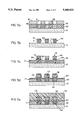
- FIGS. 5a-5d depict the method of making coils C1 and C2 of the present invention thin film magnetic head 10.
- a layer of photoresist 52 is spin coated onto insulative layer 12 using a spin coater.
- Photoresist 52 is preferably a negative or image reversal photoresist such a AZ5218.
- the photoresist layer 52 is then stabilized on the surface of layer 12 by being baked at 90° C.
- a mask "M” having holes “H” forming a spiral pattern is placed over photoresist layer 52.
- Photoresist layer 52 is then exposed to ultraviolet light of wavelengths between 260 and 436 nanometers. The ultraviolet light generates a catalyst in the exposed areas "x" of the underlying photoresist layer 52 under the spiral patterned of holes "H". By under-exposing the photoresist layer 52, the deeper regions of the spiral pattern near the edges of the spiral pattern have a lower concentration of the catalyst.
- photoresist layer 52 After exposure to light, photoresist layer 52 is baked on a hot plate to activate the catalyst in the spiral pattern 54. The unexposed regions 66 of photoresist layer 52 is then exposed and dissolved and removed by subjecting photoresist layer 52 to a developing solution. The remaining undissolved material forms a spiral resist pattern 54. Because of the under exposure, the sidewalls 64 of resist pattern 54 are undercut at a negative linear slope so that the width "w" decreases with the depth "d" of the pattern 54 as may be seen in FIG. 5b.
- copper is evaporated over photoresist pattern 54 to simultaneously form two multi-layer spiral coils.
- the metal deposited upon substrate 12 between spiral pattern 54 forms bottom coil C1 having windings 56.
- the metal deposited upon the upper surface 70 of photoresist pattern 54 forms top coil C1 having windings 58.
- the undercut sidewalls 64 of pattern 54 causes a shadowing effect so that the deposited metal does not build up at the sidewalls 64 of resist pattern 54. This prevents deposited copper from shorting out the windings 56 and 58.
- the windings 56 of coil C1 are wider at the base than at the upper surface due to the shadowing effect of the undercut sidewalls 64.
- a low viscosity insulative photoresist such as AZ1370 is deposited over coils C1 and C2 forming an insulative photoresist layer 60 which covers coils C1 and C2.
- the low viscosity of the photoresist allows the photoresist to fill in the gaps 68 between windings 56 and sidewalls 64.
- a final insulating photoresist layer 62 preferably AZ1375 or AZP4400 is deposited over insulating layer 60 to insulate and protect coils C1 and C2.
- Photoresist layers 54, 60 and 62 are then hardened by hard bake in a vacuum. Photoresist layers 54, 60 and 62 make up insulating layer 24 (FIGS. 2 and 3). The process depicted in FIGS. 5a-5e can then be repeated to add additional coil layers.
- Poles 1 and 2 are formed by depositing metal through an additive process.
- FIG. 6 depicts an alternative method of forming the photoresist pattern.
- a layer of photoresist 52' is applied and baked onto layer 12 in the same manner as depicted in FIG. 5a. However, after baking, an extra step is performed in which the upper surface 84 of photoresist layer 52' is chemically treated to harden only the upper surface 84.
- the photoresist layer 52' is then masked as before with a spiral pattern mask and exposed to ultraviolet light. When the exposed regions 66 of photoresist layer 52' are dissolved, a spiral photoresist pattern 82 (shown in cross section) having stepped side walls 80 remains. Coils C1 and C2 are then formed over pattern 82 and insulated with photoresist as depicted in FIGS. 5c through 5e to form a multi-coil structure.
- the coils of the present invention can be used as spiral inductors.
- photoresist patterns 54 and 82 can be formed using a multilayer photoresist process.
Abstract
Description
Claims (27)
Priority Applications (1)
| Application Number | Priority Date | Filing Date | Title |
|---|---|---|---|
| US08/029,125 US5448822A (en) | 1993-03-10 | 1993-03-10 | Method of making a thin film magnetic head having multi-layer coils |
Applications Claiming Priority (1)
| Application Number | Priority Date | Filing Date | Title |
|---|---|---|---|
| US08/029,125 US5448822A (en) | 1993-03-10 | 1993-03-10 | Method of making a thin film magnetic head having multi-layer coils |
Publications (1)
| Publication Number | Publication Date |
|---|---|
| US5448822A true US5448822A (en) | 1995-09-12 |
Family
ID=21847372
Family Applications (1)
| Application Number | Title | Priority Date | Filing Date |
|---|---|---|---|
| US08/029,125 Expired - Lifetime US5448822A (en) | 1993-03-10 | 1993-03-10 | Method of making a thin film magnetic head having multi-layer coils |
Country Status (1)
| Country | Link |
|---|---|
| US (1) | US5448822A (en) |
Cited By (19)
| Publication number | Priority date | Publication date | Assignee | Title |
|---|---|---|---|---|
| US5729887A (en) * | 1994-05-09 | 1998-03-24 | Daidotokushuko Kabushikikaisha | Method of manufacturing a thin-film coil |
| US5877924A (en) * | 1996-05-08 | 1999-03-02 | Nec Corporation | Thin film magnetic head including negative photoresist |
| US5883762A (en) * | 1997-03-13 | 1999-03-16 | Calhoun; Robert B. | Electroplating apparatus and process for reducing oxidation of oxidizable plating anions and cations |
| US6034848A (en) * | 1998-04-22 | 2000-03-07 | International Business Machines Corporation | Low profile multi-layer coil merged thin film magnetic head |
| US6191918B1 (en) | 1998-10-23 | 2001-02-20 | International Business Machines Corporation | Embedded dual coil planar structure |
| US6204997B1 (en) * | 1998-05-19 | 2001-03-20 | Tdk Corporation | Thin film magnetic head with a plurality of engaged thin-film coils and method of manufacturing the same |
| US6226149B1 (en) * | 1998-12-15 | 2001-05-01 | International Business Machines Corporation | Planar stitched write head having write coil insulated with inorganic insulation |
| US6240622B1 (en) * | 1999-07-09 | 2001-06-05 | Micron Technology, Inc. | Integrated circuit inductors |
| US6417998B1 (en) * | 1999-03-23 | 2002-07-09 | Read-Rite Corporation | Ultra small advanced write transducer and method for making same |
| US6452742B1 (en) | 1999-09-02 | 2002-09-17 | Read-Rite Corporation | Thin film write having reduced resistance conductor coil partially recessed within middle coat insulation |
| US6570739B2 (en) | 2000-02-10 | 2003-05-27 | International Business Machines Corporation | Magnetic head having write head element with high aspect ratio coil |
| US20030151856A1 (en) * | 2002-02-08 | 2003-08-14 | Headway Technologies, Inc. | Thin film magnetic head and method of manufacturing the same |
| US20030208900A1 (en) * | 2002-05-10 | 2003-11-13 | Liang Morris P.F. | High density multi-layer microcoil and method for fabricating the same |
| US6859997B1 (en) * | 2000-09-19 | 2005-03-01 | Western Digital (Fremont), Inc. | Method for manufacturing a magnetic write element |
| US20050045848A1 (en) * | 2003-08-29 | 2005-03-03 | Bedell Daniel Wayne | Method for patterning a self-aligned coil using a damascene process |
| US20050047014A1 (en) * | 2003-08-29 | 2005-03-03 | Bedell Daniel Wayne | Apparatus for patterning a self-aligned coil using a damascene process |
| US20050241141A1 (en) * | 2003-01-30 | 2005-11-03 | Headway Technologies, Inc. | Method of manufacturing thin-film magnetic head |
| US20080253022A1 (en) * | 2007-04-12 | 2008-10-16 | International Business Machines Corporation | Magnetic write transducer |
| US20190355676A1 (en) * | 2018-05-17 | 2019-11-21 | Advanced Semiconductor Engineering, Inc. | Semiconductor device package and method of manufacturing the same |
Citations (2)
| Publication number | Priority date | Publication date | Assignee | Title |
|---|---|---|---|---|
| US3685144A (en) * | 1967-09-18 | 1972-08-22 | Ncr Co | Method of making a magnetic transducer |
| US4684438A (en) * | 1984-02-03 | 1987-08-04 | Commissariat A L'energie Atomique | Process for producing a coil for a magnetic recording head |
-
1993
- 1993-03-10 US US08/029,125 patent/US5448822A/en not_active Expired - Lifetime
Patent Citations (2)
| Publication number | Priority date | Publication date | Assignee | Title |
|---|---|---|---|---|
| US3685144A (en) * | 1967-09-18 | 1972-08-22 | Ncr Co | Method of making a magnetic transducer |
| US4684438A (en) * | 1984-02-03 | 1987-08-04 | Commissariat A L'energie Atomique | Process for producing a coil for a magnetic recording head |
Non-Patent Citations (6)
| Title |
|---|
| Holger Moritz, IEEE Transactions on Electron Devices, vol. ED 32, No. 3, Mar. 1985, 672 676, Optical Single Layer Lift Off Process . * |
| Holger Moritz, IEEE Transactions on Electron Devices, vol. ED-32, No. 3, Mar. 1985, 672-676, "Optical Single Layer Lift-Off Process". |
| M. Hatzakis et al., IBM J. Res. Develop., 24(4), Jul., 1980, 452 460, Single Step Optical Lift Off Process . * |
| M. Hatzakis et al., IBM J. Res. Develop., 24(4), Jul., 1980, 452-460, "Single-Step Optical Lift-Off Process". |
| M. Spak, et al., As presented at: Seventh International Technical Conference on Photopolymers, Ellenville, N.Y., "Mechanism and Lithographic Evaluation of Image Reversal in AZ 5214 Photoresist". |
| M. Spak, et al., As presented at: Seventh International Technical Conference on Photopolymers, Ellenville, N.Y., Mechanism and Lithographic Evaluation of Image Reversal in AZ 5214 Photoresist . * |
Cited By (55)
| Publication number | Priority date | Publication date | Assignee | Title |
|---|---|---|---|---|
| US5729887A (en) * | 1994-05-09 | 1998-03-24 | Daidotokushuko Kabushikikaisha | Method of manufacturing a thin-film coil |
| US5877924A (en) * | 1996-05-08 | 1999-03-02 | Nec Corporation | Thin film magnetic head including negative photoresist |
| US6107005A (en) * | 1996-05-08 | 2000-08-22 | Nec Corporation | Method of application of a thin film magnetic head including a negative photoresist |
| US5883762A (en) * | 1997-03-13 | 1999-03-16 | Calhoun; Robert B. | Electroplating apparatus and process for reducing oxidation of oxidizable plating anions and cations |
| US6034848A (en) * | 1998-04-22 | 2000-03-07 | International Business Machines Corporation | Low profile multi-layer coil merged thin film magnetic head |
| US6325947B1 (en) | 1998-04-22 | 2001-12-04 | International Business Machines Corporation | Method for forming low profile multi-layer coil merged thin film magnetic head |
| US6204997B1 (en) * | 1998-05-19 | 2001-03-20 | Tdk Corporation | Thin film magnetic head with a plurality of engaged thin-film coils and method of manufacturing the same |
| US6191918B1 (en) | 1998-10-23 | 2001-02-20 | International Business Machines Corporation | Embedded dual coil planar structure |
| US6338939B1 (en) | 1998-10-23 | 2002-01-15 | International Business Machines Corporation | Embedded dual coil fabrication process |
| US6377423B2 (en) * | 1998-12-15 | 2002-04-23 | International Business Machines Corporation | Planar stitched write head having write coil insulated with inorganic insulation |
| US6226149B1 (en) * | 1998-12-15 | 2001-05-01 | International Business Machines Corporation | Planar stitched write head having write coil insulated with inorganic insulation |
| US6417998B1 (en) * | 1999-03-23 | 2002-07-09 | Read-Rite Corporation | Ultra small advanced write transducer and method for making same |
| US6646534B2 (en) | 1999-07-09 | 2003-11-11 | Micron Technology, Inc. | Integrated circuit inductors |
| US7158004B2 (en) | 1999-07-09 | 2007-01-02 | Micron Technology, Inc. | Integrated circuit inductors |
| US20020095776A1 (en) * | 1999-07-09 | 2002-07-25 | Micron Technology, Inc. | Integrated circuit inductors |
| US20020095770A1 (en) * | 1999-07-09 | 2002-07-25 | Micron Technology, Inc. | Integrated circuit inductors |
| US20020095771A1 (en) * | 1999-07-09 | 2002-07-25 | Micron Technology, Inc. | Integrated circuit inductors |
| US20020095778A1 (en) * | 1999-07-09 | 2002-07-25 | Micron Technology, Inc. | Integrated circuit inductors |
| US20020095769A1 (en) * | 1999-07-09 | 2002-07-25 | Micron Technology, Inc. | Integrated circuit inductors |
| US20020095768A1 (en) * | 1999-07-09 | 2002-07-25 | Micron Technology, Inc. | Integrated circuit inductors |
| US20020095772A1 (en) * | 1999-07-09 | 2002-07-25 | Micron Technology, Inc. | Integrated circuit inductors |
| US20020095775A1 (en) * | 1999-07-09 | 2002-07-25 | Micron Technology, Inc. | Integrated circuit inductors |
| US6446327B2 (en) | 1999-07-09 | 2002-09-10 | Kie Y. Ahn | Integrated circuit inductors |
| US6357107B2 (en) | 1999-07-09 | 2002-03-19 | Micron Technology, Inc. | Integrated circuit inductors |
| US7388462B2 (en) | 1999-07-09 | 2008-06-17 | Micron Technology, Inc. | Integrated circuit inductors |
| US6900716B2 (en) | 1999-07-09 | 2005-05-31 | Micron Technology, Inc. | Integrated circuit inductors |
| US6612019B2 (en) | 1999-07-09 | 2003-09-02 | Micron Technology, Inc. | Integrated circuit inductors |
| US6240622B1 (en) * | 1999-07-09 | 2001-06-05 | Micron Technology, Inc. | Integrated circuit inductors |
| US6976300B2 (en) | 1999-07-09 | 2005-12-20 | Micron Technology, Inc. | Integrated circuit inductors |
| US6701607B2 (en) | 1999-07-09 | 2004-03-09 | Micron Technology, Inc. | Integrated circuit inductors |
| US6762478B2 (en) | 1999-07-09 | 2004-07-13 | Micron Technology, Inc. | Integrated circuit inductors |
| US6760967B2 (en) | 1999-07-09 | 2004-07-13 | Micron Technology, Inc. | Integrated circuit inductors |
| US6779250B2 (en) | 1999-07-09 | 2004-08-24 | Micron Technology, Inc. | Integrated circuit inductors |
| US6948230B2 (en) | 1999-07-09 | 2005-09-27 | Micron Technology, Inc. | Integrated circuit inductors |
| US6817087B2 (en) | 1999-07-09 | 2004-11-16 | Micron Technology, Inc. | Integrated circuit inductors |
| US6822545B2 (en) | 1999-07-09 | 2004-11-23 | Micron Technology, Inc. | Integrated circuit inductors |
| US6825747B2 (en) | 1999-07-09 | 2004-11-30 | Micron Technology, Inc. | Integrated circuit inductors |
| US6910260B2 (en) | 1999-07-09 | 2005-06-28 | Micron Technology, Inc. | Integrated circuit inductors |
| US6452742B1 (en) | 1999-09-02 | 2002-09-17 | Read-Rite Corporation | Thin film write having reduced resistance conductor coil partially recessed within middle coat insulation |
| US6570739B2 (en) | 2000-02-10 | 2003-05-27 | International Business Machines Corporation | Magnetic head having write head element with high aspect ratio coil |
| US6859997B1 (en) * | 2000-09-19 | 2005-03-01 | Western Digital (Fremont), Inc. | Method for manufacturing a magnetic write element |
| US6801407B2 (en) * | 2002-02-08 | 2004-10-05 | Headway Technologies, Incorporated | Thin film magnetic head and method of manufacturing the same |
| US20030151856A1 (en) * | 2002-02-08 | 2003-08-14 | Headway Technologies, Inc. | Thin film magnetic head and method of manufacturing the same |
| US20030208900A1 (en) * | 2002-05-10 | 2003-11-13 | Liang Morris P.F. | High density multi-layer microcoil and method for fabricating the same |
| US6876285B2 (en) * | 2002-05-10 | 2005-04-05 | Industrial Technology Research Institute | High density multi-layer microcoil and method for fabricating the same |
| US7526857B2 (en) * | 2003-01-30 | 2009-05-05 | Headway Technologies, Inc. | Method of manufacturing thin-film magnetic head |
| US20050241141A1 (en) * | 2003-01-30 | 2005-11-03 | Headway Technologies, Inc. | Method of manufacturing thin-film magnetic head |
| US7022248B2 (en) | 2003-08-29 | 2006-04-04 | Hitachi Global Storage Technologies Netherlands B.V. | Method for patterning a self-aligned coil using a damascene process |
| US7075750B2 (en) | 2003-08-29 | 2006-07-11 | Hitachi Global Storage Technologies Netherlands B.V. | Apparatus for patterning a self-aligned coil using a damascene process |
| US20050045848A1 (en) * | 2003-08-29 | 2005-03-03 | Bedell Daniel Wayne | Method for patterning a self-aligned coil using a damascene process |
| US20050047014A1 (en) * | 2003-08-29 | 2005-03-03 | Bedell Daniel Wayne | Apparatus for patterning a self-aligned coil using a damascene process |
| US20080253022A1 (en) * | 2007-04-12 | 2008-10-16 | International Business Machines Corporation | Magnetic write transducer |
| US8004792B2 (en) | 2007-04-12 | 2011-08-23 | International Business Machines Corporation | Magnetic write transducer |
| US20190355676A1 (en) * | 2018-05-17 | 2019-11-21 | Advanced Semiconductor Engineering, Inc. | Semiconductor device package and method of manufacturing the same |
| US11393776B2 (en) * | 2018-05-17 | 2022-07-19 | Advanced Semiconductor Engineering, Inc. | Semiconductor device package and method of manufacturing the same |
Similar Documents
| Publication | Publication Date | Title |
|---|---|---|
| US5448822A (en) | Method of making a thin film magnetic head having multi-layer coils | |
| US5529831A (en) | Thin film device | |
| US7307503B2 (en) | Thin film coil, method of manufacturing the same, coil structure, and method of manufacturing the same | |
| US5065270A (en) | Thin film magnetic recording head with a low resistance coil formed by two processes | |
| US4165525A (en) | Magnetic head having a core provided on a substrate by means of thin-film technology | |
| KR940005555B1 (en) | Thin film magnetic head | |
| US4298436A (en) | Method of forming insulated conductors in a conductive medium and article thus formed | |
| JP2002525869A (en) | Method for manufacturing semiconductor device having semiconductor substrate having surface on which coil having magnetic core is provided | |
| JP2001284533A (en) | On-chip coil md its manufacturing method | |
| JPH04216310A (en) | Thin film magnetic head and manufacture thereof | |
| JPS63283004A (en) | Flat surface inductor and manufacture thereof | |
| JP2003133136A5 (en) | ||
| JP2747099B2 (en) | Thin film magnetic head | |
| JPH05242430A (en) | Manufacture of thin film magnetic head | |
| JPH07118849A (en) | Formation of conductor thin-film pattern | |
| JP2007242220A (en) | Perpendicular magnetic recording head and method of manufacturing the same | |
| JPH02132616A (en) | Thin film magnetic head | |
| JPH06176318A (en) | Coil formation of thin-film magnetic head | |
| JP2007328881A (en) | Magnetic head and its manufacturing method | |
| JPH04344311A (en) | Thin film magnetic circuit substrate and magnetic head using the same | |
| JP2000048317A (en) | Thin film magnetic head | |
| JPH01159816A (en) | Magnetic head | |
| KR100192477B1 (en) | Structure and manufacturing method for transformer of ic chip | |
| JPH0745476A (en) | Lc filter and fabrication thereof | |
| JPS63239608A (en) | Conductor coil for thin film magnetic head and its production |
Legal Events
| Date | Code | Title | Description |
|---|---|---|---|
| AS | Assignment |
Owner name: DIGITAL EQUIPMENT CORPORATION, MASSACHUSETTS Free format text: ASSIGNMENT OF ASSIGNORS INTEREST.;ASSIGNORS:WU, ANDREW L.;DUVAL, PAUL J.;REEL/FRAME:006463/0426 Effective date: 19930309 |
|
| AS | Assignment |
Owner name: QUANTUM CORPORATION Free format text: ASSIGNMENT OF ASSIGNORS INTEREST;ASSIGNOR:DIGITAL EQUIPMENT CORPORATION;REEL/FRAME:007156/0665 Effective date: 19941003 Owner name: CANADIAN IMPERIAL BANK OF COMMERCE, AS ADMINIST Free format text: SECURITY INTEREST;ASSIGNOR:QUANTUM CORPORATION;REEL/FRAME:007152/0815 Effective date: 19941003 |
|
| STPP | Information on status: patent application and granting procedure in general |
Free format text: APPLICATION UNDERGOING PREEXAM PROCESSING |
|
| AS | Assignment |
Owner name: CANADIAN IMPERIAL BANK OF COMMERCE, NEW YORK Free format text: SECURITY INTEREST;ASSIGNOR:QUANTUM CORPORATION;REEL/FRAME:008222/0215 Effective date: 19961003 |
|
| AS | Assignment |
Owner name: CANADIAN IMPERIAL BANK, AS ADMINISTRATIVE AGENT, N Free format text: RELEASE;ASSIGNOR:QUANTUM CORPORATION;REEL/FRAME:008744/0904 Effective date: 19970818 |
|
| FEPP | Fee payment procedure |
Free format text: PAYOR NUMBER ASSIGNED (ORIGINAL EVENT CODE: ASPN); ENTITY STATUS OF PATENT OWNER: LARGE ENTITY |
|
| FPAY | Fee payment |
Year of fee payment: 4 |
|
| AS | Assignment |
Owner name: MAXTOR CORPORATION, CALIFORNIA Free format text: ASSIGNMENT OF ASSIGNORS INTEREST;ASSIGNOR:QUANTUM CORPORATION;REEL/FRAME:012653/0726 Effective date: 20010724 |
|
| FPAY | Fee payment |
Year of fee payment: 8 |
|
| FPAY | Fee payment |
Year of fee payment: 12 |
|
| AS | Assignment |
Owner name: JPMORGAN CHASE BANK, N.A., AS ADMINISTRATIVE AGENT Free format text: SECURITY AGREEMENT;ASSIGNORS:MAXTOR CORPORATION;SEAGATE TECHNOLOGY LLC;SEAGATE TECHNOLOGY INTERNATIONAL;REEL/FRAME:022757/0017 Effective date: 20090507 Owner name: WELLS FARGO BANK, NATIONAL ASSOCIATION, AS COLLATE Free format text: SECURITY AGREEMENT;ASSIGNORS:MAXTOR CORPORATION;SEAGATE TECHNOLOGY LLC;SEAGATE TECHNOLOGY INTERNATIONAL;REEL/FRAME:022757/0017 Effective date: 20090507 |
|
| AS | Assignment |
Owner name: SEAGATE TECHNOLOGY HDD HOLDINGS, CALIFORNIA Free format text: RELEASE;ASSIGNOR:JPMORGAN CHASE BANK, N.A., AS ADMINISTRATIVE AGENT;REEL/FRAME:025662/0001 Effective date: 20110114 Owner name: MAXTOR CORPORATION, CALIFORNIA Free format text: RELEASE;ASSIGNOR:JPMORGAN CHASE BANK, N.A., AS ADMINISTRATIVE AGENT;REEL/FRAME:025662/0001 Effective date: 20110114 Owner name: SEAGATE TECHNOLOGY LLC, CALIFORNIA Free format text: RELEASE;ASSIGNOR:JPMORGAN CHASE BANK, N.A., AS ADMINISTRATIVE AGENT;REEL/FRAME:025662/0001 Effective date: 20110114 Owner name: SEAGATE TECHNOLOGY INTERNATIONAL, CALIFORNIA Free format text: RELEASE;ASSIGNOR:JPMORGAN CHASE BANK, N.A., AS ADMINISTRATIVE AGENT;REEL/FRAME:025662/0001 Effective date: 20110114 |
|
| AS | Assignment |
Owner name: THE BANK OF NOVA SCOTIA, AS ADMINISTRATIVE AGENT, Free format text: SECURITY AGREEMENT;ASSIGNOR:SEAGATE TECHNOLOGY LLC;REEL/FRAME:026010/0350 Effective date: 20110118 |
|
| AS | Assignment |
Owner name: SEAGATE TECHNOLOGY LLC, CALIFORNIA Free format text: TERMINATION AND RELEASE OF SECURITY INTEREST IN PATENT RIGHTS;ASSIGNOR:WELLS FARGO BANK, NATIONAL ASSOCIATION, AS COLLATERAL AGENT AND SECOND PRIORITY REPRESENTATIVE;REEL/FRAME:030833/0001 Effective date: 20130312 Owner name: SEAGATE TECHNOLOGY US HOLDINGS, INC., CALIFORNIA Free format text: TERMINATION AND RELEASE OF SECURITY INTEREST IN PATENT RIGHTS;ASSIGNOR:WELLS FARGO BANK, NATIONAL ASSOCIATION, AS COLLATERAL AGENT AND SECOND PRIORITY REPRESENTATIVE;REEL/FRAME:030833/0001 Effective date: 20130312 Owner name: SEAGATE TECHNOLOGY INTERNATIONAL, CAYMAN ISLANDS Free format text: TERMINATION AND RELEASE OF SECURITY INTEREST IN PATENT RIGHTS;ASSIGNOR:WELLS FARGO BANK, NATIONAL ASSOCIATION, AS COLLATERAL AGENT AND SECOND PRIORITY REPRESENTATIVE;REEL/FRAME:030833/0001 Effective date: 20130312 Owner name: EVAULT INC. (F/K/A I365 INC.), CALIFORNIA Free format text: TERMINATION AND RELEASE OF SECURITY INTEREST IN PATENT RIGHTS;ASSIGNOR:WELLS FARGO BANK, NATIONAL ASSOCIATION, AS COLLATERAL AGENT AND SECOND PRIORITY REPRESENTATIVE;REEL/FRAME:030833/0001 Effective date: 20130312 |