US5448090A - Structure for reducing parasitic leakage in a memory array with merged isolation and node trench construction - Google Patents
Structure for reducing parasitic leakage in a memory array with merged isolation and node trench construction Download PDFInfo
- Publication number
- US5448090A US5448090A US08/285,480 US28548094A US5448090A US 5448090 A US5448090 A US 5448090A US 28548094 A US28548094 A US 28548094A US 5448090 A US5448090 A US 5448090A
- Authority
- US
- United States
- Prior art keywords
- trench
- region
- charge storage
- isolation
- semiconductor substrate
- Prior art date
- Legal status (The legal status is an assumption and is not a legal conclusion. Google has not performed a legal analysis and makes no representation as to the accuracy of the status listed.)
- Expired - Lifetime
Links
- 238000002955 isolation Methods 0.000 title claims abstract description 135
- 238000010276 construction Methods 0.000 title claims abstract description 19
- 230000003071 parasitic effect Effects 0.000 title abstract description 19
- 238000003860 storage Methods 0.000 claims abstract description 88
- 239000004065 semiconductor Substances 0.000 claims abstract description 83
- 239000000758 substrate Substances 0.000 claims abstract description 65
- 238000009792 diffusion process Methods 0.000 claims abstract description 51
- 239000007943 implant Substances 0.000 claims abstract description 45
- 230000015572 biosynthetic process Effects 0.000 claims description 16
- 239000002019 doping agent Substances 0.000 claims description 16
- 239000003990 capacitor Substances 0.000 claims description 14
- 239000000463 material Substances 0.000 claims description 14
- 238000012546 transfer Methods 0.000 claims description 7
- 230000006870 function Effects 0.000 claims description 5
- 230000002411 adverse Effects 0.000 claims 1
- 230000002452 interceptive effect Effects 0.000 claims 1
- 238000004519 manufacturing process Methods 0.000 abstract description 15
- 238000002513 implantation Methods 0.000 abstract description 7
- 230000007246 mechanism Effects 0.000 abstract description 6
- 229910052710 silicon Inorganic materials 0.000 description 9
- 239000010703 silicon Substances 0.000 description 9
- XUIMIQQOPSSXEZ-UHFFFAOYSA-N Silicon Chemical compound [Si] XUIMIQQOPSSXEZ-UHFFFAOYSA-N 0.000 description 8
- 238000000034 method Methods 0.000 description 8
- 229910021420 polycrystalline silicon Inorganic materials 0.000 description 8
- 229920005591 polysilicon Polymers 0.000 description 8
- 239000002131 composite material Substances 0.000 description 5
- 230000009977 dual effect Effects 0.000 description 5
- 238000012545 processing Methods 0.000 description 4
- 238000003491 array Methods 0.000 description 3
- 229910052785 arsenic Inorganic materials 0.000 description 3
- RQNWIZPPADIBDY-UHFFFAOYSA-N arsenic atom Chemical compound [As] RQNWIZPPADIBDY-UHFFFAOYSA-N 0.000 description 3
- 150000004767 nitrides Chemical class 0.000 description 3
- 229910052782 aluminium Inorganic materials 0.000 description 2
- XAGFODPZIPBFFR-UHFFFAOYSA-N aluminium Chemical compound [Al] XAGFODPZIPBFFR-UHFFFAOYSA-N 0.000 description 2
- 238000013459 approach Methods 0.000 description 2
- 230000008021 deposition Effects 0.000 description 2
- 230000005669 field effect Effects 0.000 description 2
- 238000012986 modification Methods 0.000 description 2
- 230000004048 modification Effects 0.000 description 2
- 229920002120 photoresistant polymer Polymers 0.000 description 2
- 230000009467 reduction Effects 0.000 description 2
- ZOXJGFHDIHLPTG-UHFFFAOYSA-N Boron Chemical compound [B] ZOXJGFHDIHLPTG-UHFFFAOYSA-N 0.000 description 1
- OAICVXFJPJFONN-UHFFFAOYSA-N Phosphorus Chemical compound [P] OAICVXFJPJFONN-UHFFFAOYSA-N 0.000 description 1
- 230000000903 blocking effect Effects 0.000 description 1
- 229910052796 boron Inorganic materials 0.000 description 1
- 238000011161 development Methods 0.000 description 1
- 230000000694 effects Effects 0.000 description 1
- 238000005530 etching Methods 0.000 description 1
- 238000010438 heat treatment Methods 0.000 description 1
- BHEPBYXIRTUNPN-UHFFFAOYSA-N hydridophosphorus(.) (triplet) Chemical compound [PH] BHEPBYXIRTUNPN-UHFFFAOYSA-N 0.000 description 1
- 239000012535 impurity Substances 0.000 description 1
- 229910052738 indium Inorganic materials 0.000 description 1
- APFVFJFRJDLVQX-UHFFFAOYSA-N indium atom Chemical compound [In] APFVFJFRJDLVQX-UHFFFAOYSA-N 0.000 description 1
- 238000009413 insulation Methods 0.000 description 1
- 238000005468 ion implantation Methods 0.000 description 1
- 238000000059 patterning Methods 0.000 description 1
- 229910052698 phosphorus Inorganic materials 0.000 description 1
- 239000011574 phosphorus Substances 0.000 description 1
- 230000008569 process Effects 0.000 description 1
- MAKDTFFYCIMFQP-UHFFFAOYSA-N titanium tungsten Chemical compound [Ti].[W] MAKDTFFYCIMFQP-UHFFFAOYSA-N 0.000 description 1
- WQJQOUPTWCFRMM-UHFFFAOYSA-N tungsten disilicide Chemical compound [Si]#[W]#[Si] WQJQOUPTWCFRMM-UHFFFAOYSA-N 0.000 description 1
- 229910021342 tungsten silicide Inorganic materials 0.000 description 1
Images


Classifications
-
- C—CHEMISTRY; METALLURGY
- C23—COATING METALLIC MATERIAL; COATING MATERIAL WITH METALLIC MATERIAL; CHEMICAL SURFACE TREATMENT; DIFFUSION TREATMENT OF METALLIC MATERIAL; COATING BY VACUUM EVAPORATION, BY SPUTTERING, BY ION IMPLANTATION OR BY CHEMICAL VAPOUR DEPOSITION, IN GENERAL; INHIBITING CORROSION OF METALLIC MATERIAL OR INCRUSTATION IN GENERAL
- C23C—COATING METALLIC MATERIAL; COATING MATERIAL WITH METALLIC MATERIAL; SURFACE TREATMENT OF METALLIC MATERIAL BY DIFFUSION INTO THE SURFACE, BY CHEMICAL CONVERSION OR SUBSTITUTION; COATING BY VACUUM EVAPORATION, BY SPUTTERING, BY ION IMPLANTATION OR BY CHEMICAL VAPOUR DEPOSITION, IN GENERAL
- C23C14/00—Coating by vacuum evaporation, by sputtering or by ion implantation of the coating forming material
- C23C14/22—Coating by vacuum evaporation, by sputtering or by ion implantation of the coating forming material characterised by the process of coating
- C23C14/48—Ion implantation
-
- H—ELECTRICITY
- H01—ELECTRIC ELEMENTS
- H01L—SEMICONDUCTOR DEVICES NOT COVERED BY CLASS H10
- H01L21/00—Processes or apparatus adapted for the manufacture or treatment of semiconductor or solid state devices or of parts thereof
- H01L21/70—Manufacture or treatment of devices consisting of a plurality of solid state components formed in or on a common substrate or of parts thereof; Manufacture of integrated circuit devices or of parts thereof
- H01L21/71—Manufacture of specific parts of devices defined in group H01L21/70
- H01L21/76—Making of isolation regions between components
- H01L21/762—Dielectric regions, e.g. EPIC dielectric isolation, LOCOS; Trench refilling techniques, SOI technology, use of channel stoppers
- H01L21/76224—Dielectric regions, e.g. EPIC dielectric isolation, LOCOS; Trench refilling techniques, SOI technology, use of channel stoppers using trench refilling with dielectric materials
- H01L21/76237—Dielectric regions, e.g. EPIC dielectric isolation, LOCOS; Trench refilling techniques, SOI technology, use of channel stoppers using trench refilling with dielectric materials introducing impurities in trench side or bottom walls, e.g. for forming channel stoppers or alter isolation behavior
-
- H—ELECTRICITY
- H10—SEMICONDUCTOR DEVICES; ELECTRIC SOLID-STATE DEVICES NOT OTHERWISE PROVIDED FOR
- H10B—ELECTRONIC MEMORY DEVICES
- H10B12/00—Dynamic random access memory [DRAM] devices
- H10B12/01—Manufacture or treatment
- H10B12/02—Manufacture or treatment for one transistor one-capacitor [1T-1C] memory cells
- H10B12/03—Making the capacitor or connections thereto
- H10B12/038—Making the capacitor or connections thereto the capacitor being in a trench in the substrate
-
- H—ELECTRICITY
- H10—SEMICONDUCTOR DEVICES; ELECTRIC SOLID-STATE DEVICES NOT OTHERWISE PROVIDED FOR
- H10B—ELECTRONIC MEMORY DEVICES
- H10B12/00—Dynamic random access memory [DRAM] devices
- H10B12/30—DRAM devices comprising one-transistor - one-capacitor [1T-1C] memory cells
- H10B12/37—DRAM devices comprising one-transistor - one-capacitor [1T-1C] memory cells the capacitor being at least partially in a trench in the substrate
- H10B12/373—DRAM devices comprising one-transistor - one-capacitor [1T-1C] memory cells the capacitor being at least partially in a trench in the substrate the capacitor extending under or around the transistor
-
- H—ELECTRICITY
- H10—SEMICONDUCTOR DEVICES; ELECTRIC SOLID-STATE DEVICES NOT OTHERWISE PROVIDED FOR
- H10B—ELECTRONIC MEMORY DEVICES
- H10B99/00—Subject matter not provided for in other groups of this subclass
Definitions
- the present invention relates to a semiconductor memory structure with merged isolation trench and node trench construction having reduced parasitic charge leakage, and to a method of fabricating the same.
- MOSFETs metal-oxide-silicon field-effect transistors
- MOSFETs are said to be "self-isolated;” that is, as long as the source-substrate and drain-substrate pn junctions are held at reverse bias, drain current is due only to current flow from source to drain through a channel under the gate.
- MOS metal-oxide-semiconductor
- the conducting lines used to interconnect metal-oxide-semiconductor (MOS) transistors often form gates of parasitic MOS transistors within the common silicon substrate, with the oxide beneath them forming an undesired gate oxide.
- MOSFETs it is necessary to prevent the formation of channels in the field regions.
- One way to accomplish this is to utilize a comparatively thick field oxide layer. However, as device dimensions continue to shrink, thick field oxide regions become undesirable.
- Another transistor isolation technique is to raise the dopant level in the substrate beneath the field oxide to increase the parasitic gate turn-on voltage. This is typically accomplished by ion implantation to create what are referred to in the art as “field isolation regions" or “channel stop regions.”
- field isolation regions or “channel stop regions.”
- the combination of field oxide and a channel stop region can provide adequate isolation for most PMOS, NMOS and oxide-isolated bipolar integrated circuits.
- the formation of channel stop regions in certain applications is not without drawbacks.
- FIGS. 1a & 1b depict one embodiment of a metal-oxide-semiconductor field-effect transistor (MOSFET), generally denoted 10, comprised of opposing source and drain regions 12 and 14, respectively.
- MOSFET metal-oxide-semiconductor field-effect transistor
- Source region 12 and drain region 14 are isolated from each other by a trench isolation oxide 16, and are isolated from an overpassing gate 17.
- An appropriate blocking type implant is disposed in the area beneath trench oxide 16 to define a channel stop region 20 in a substrate 22.
- the channel stop implant concentration is chosen to impair formation of the parasitic thick oxide MOSFET, while at the same time minimizing impact on the electrical characteristics of the source/drain diffusions. This can be difficult, however, since heating of a semiconductor wafer during processing after forming channel stop regions can cause the implantations to migrate towards the diffusions or into the field oxide. This difficulty tends to limit the concentration of dopant in the channel stop region.
- One significant application for channel stop regions has been in the formation of semiconductor memory devices.
- MINT merged isolation and node trench
- the present invention comprises in a first aspect a semiconductor structure including a semiconductor substrate having a charge storage trench disposed therein that is at least partially surrounded by a field isolation region that is also disposed in the semiconductor substrate.
- the charge storage trench and the field isolation region have an interface region wherein the charge storage trench and the field isolation region are in opposing relation.
- a first diffusion region and a second diffusion region are also located in the semiconductor substrate and disposed so as to be partially separated from the charge storage trench by the field isolation region proximate to the interface region.
- An isolation implant layer is formed in the field isolation region at the interface region of the charge storage trench and the field isolation region.
- the isolation implant layer is disposed and has a dopant concentration sufficient to restrict formation of an inversion layer in the field isolation region between the first diffusion region and the second diffusion region.
- the invention comprises a semiconductor memory array including a semiconductor substrate having multiple memory cells disposed in an array configuration within the substrate.
- the array is accessed through multiple intersecting word lines and bit lines.
- Each memory cell in the array includes a charge storage trench formed within the semiconductor substrate and a field isolation region that at least partially surrounds the charge storage trench such that an interface region is created between the charge storage trench and the field isolation region wherein the charge storage trench and the field isolation region are in opposing relation.
- a storage node diffusion and a bit line contact diffusion are each disposed in the substrate proximate to the charge storage trench.
- An isolation implant layer is formed in the field isolation region at the interface region of the charge storage trench and the field isolation region and has a dopant concentration sufficient to restrict formation of an inversion layer in said field isolation region between the storage node diffusion and the bit line contact diffusion of an adjacent memory cell in the array.
- a method for fabricating a memory structure which includes the steps of: forming a trench in a semiconductor substrate, the trench having a sidewall surface area and being formed near a field isolation region in the substrate; selectively implanting dopant into the sidewall of the trench near an upper surface of the semiconductor substrate so as to define an isolation implant layer in the substrate; forming a capacitor node in the trench; and forming a first and second diffusion region in the substrate.
- the first and second diffusion region are separated by the field isolation region proximate to the capacitor node formed in the trench.
- the isolation implant layer is disposed and has sufficient dopant concentration to restrict formation of an inversion layer within the field isolation region adjacent to the capacitor node and extending between the first diffusion region and the second diffusion region.
- a method for restricting formation of an inversion layer in a field isolation layer of a semiconductor memory structure having merged isolation and node trench construction includes a node trench, an isolation trench partially merged therewith, a first diffusion, and an adjacent second diffusion.
- An interface region is defined in the field isolation region at the intersection of the node trench and the isolation trench.
- the method includes the steps of: implanting additional dopant into the field isolation region at the interface region, the additional dopant being of the same type material as that of the field isolation region; and driving the additional dopant into the field isolation region at the interface region to create an isolation implant layer adjacent to the node trench and the isolation trench sufficient to restrict formation of an inversion layer between the first diffusion and the adjacent second diffusion.
- the present invention comprises in one aspect an improved memory structure with MINT construction, having trench isolation and method of fabrication, having longer charge storage capacity.
- MINT construction having trench isolation and method of fabrication, having longer charge storage capacity.
- cell refreshing may occur at longer time periods, thereby reducing power consumption of an entire memory array.
- a reduced amount of thermal energy is generated due to the longer storage capacity.
- the structure and method presented herein allow the reduction in parasitic leakage to levels which will make production level fabrication of MINT memory arrays practical. The approach applies equally to DRAMs, SRAMs, EPROMs, etc.
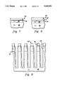
- FIG. 1a is a top plan view of a conventional MOSFET layout
- FIG. 1b is a cross-sectional elevational view of the MOSFET of FIG. 1a taken along lines 1b--1b';
- FIG. 2 is a simplified, partial perspective of a semiconductor memory structure with merged isolation and node trench (MINT) construction, showing the parasitic leakage path identified herein;
- MINT isolation and node trench
- FIG. 3a is a top plan view of the semiconductor memory structure of FIG. 2;
- FIG. 3b is a cross-sectional elevational view of the semiconductor memory structure of FIG. 3a taken along lines 3b--3b';
- FIG. 3c is a cross-sectional elevational view of the semiconductor memory structure of FIG. 3a taken along lines 3c--3c';
- FIG. 4 is a top plan view of a dynamic random access memory (DRAM) array with merged isolation trench and node trench construction, showing the parasitic leakage path identified herein;
- DRAM dynamic random access memory
- FIG. 5 is a cutaway perspective view of the dynamic random access memory array of FIG. 4 taken along lines 5--5';
- FIG. 6 is a cutaway perspective view of the dynamic random access memory array of FIG. 4 taken along lines 6--6';
- FIG. 7 is a cross-sectional elevational view of a semiconductor structure useful in describing fabrication processing in accordance with the present invention.
- FIG. 8 is a cross-sectional elevational view of the semiconductor structure of FIG. 7 subsequent to oxide mask formation
- FIG. 9 is a cross-sectional elevational view of the semiconductor structure of FIG. 8 subsequent to formation of deep substrate trenches and trench screen oxide;
- FIG. 10a is a top plan view of a charge storage trench in accordance with the present invention for a memory structure of MINT construction, showing disposition of an isolation implant layer (indicated by ⁇ x ⁇ s) at opposite ends of the charge storage trench; and
- FIG. 10b is a partial cross-sectional elevational view of the charge storage trench of FIG. 10a showing angled implantation of additional species into the field isolation region of the semiconductor structure to create the isolation implant layer.
- a parasitic leakage mechanism has been discovered by applicants occurring in memory arrays having merged isolation and node trench construction.
- the leakage mechanism is small, for example, on the order of 1 femtoamp to 1 picoamp per memory cell, but in a memory array is a significant hindrance to the goal of maintaining charge storage for a long time interval.
- the leakage path has been discovered to extend between an adjacent bit line contact diffusion and a storage node's drain or source diffusion proximate to the storage node trench and below the isolation trench.
- there is a dual gating affect which is sufficient to create an inversion layer in the field isolation region (i.e., channel stop region), notwithstanding that the field isolation region is doped to prevent such an inversion layer. This is partially due to the practical limitations on doping concentrations which may be employed in the field isolation region.
- the leakage path mechanism has been identified as passing in the field isolation region between the shallow isolation trench and the deep storage trench.
- the passing word line acts as an FET gate across the isolation oxide while the storage node operates as a gate across its own trench oxide.
- the strength of the dual gating is such as to create the parasitic inversion in the field isolation region of the memory cell adjacent to the storage node and below the isolation trench.
- this newly identified leakage mechanism is inhibited by the selective formation of an isolation implant layer on the deep trench sidewall in the vicinity of the isolation trench.
- the parasitic leakage mechanism is established when the memory cell diffusion adjacent to the storage node is at a low potential and the bit line contact diffusion of an adjacent bit line is at a high potential such that there is a source to drain bias.
- a leakage current passes when there is a low voltage in the cell's storage node and the passing word line happens to also be at a low voltage, for example, when reading or writing a cell in the array.
- this leakage current arises at the intersection of the deep storage node, the shallow isolation trench and the passing word line. If only one of the dual gates is active low then the parasitic leakage current is believed sufficiently low so as not to be a concern, at least not today. However, the present invention also addresses such a situation, which may become important in the future.
- FIGS. 2 & 3a-3c A simplified memory structure with MINT construction is partially depicted in FIGS. 2 & 3a-3c.
- This memory structure includes a deep trench capacitor 28 formed in a composite semiconductor substrate 25 comprising, for example, an n-well 29 disposed in a p+ substrate 30.
- n-well 29 functions as a field isolation region.
- a transistor is constructed having a source diffusion 31, a drain diffusion 32, and a gate electrode 34.
- Source diffusion 31 and drain diffusion 32 are separated from each other by a shallow isolation trench 33 and are separated from gate electrode 34 via a thin insulating layer disposed above the source diffusion and drain diffusion.
- the deep trench capacitor formed in composite substrate 25 includes a thin insulation layer 27 lining that is filled with, for example, polysilicon.
- Field isolation region 29 serves to separate the deep trench capacitor from adjacent deep trenches and from other structures in an array of such memory cells.
- a parasitic leakage path 40 has been discovered to arise in the memory structure of FIGS. 2 & 3a-3c when a low voltage, e.g., near ground potential, is applied to trench capacitor 28 and to the polysilicon word line 34 overpassing the isolation trench oxide 33, notwithstanding the presence of field isolation region 29.
- line 34 and capacitor 28 establish leakage path 40 by synergistically providing the parasitic FET turn-on voltage.
- the path of this inversion layer 40 extends from source diffusion 31 down the sidewall of isolation trench 33 adjacent to the storage trench 28, then continues along the bottom of the isolation trench, again adjacent to the storage trench, and finally proceeds up the isolation trench sidewall to terminate at drain diffusion 32.
- the dual gating affect has been discovered to substantially lower the threshold voltage of the parasitic thick oxide FET device such that inversion layer 40 can often occur during normal operation of the MINT memory device.
- the structure and process presented herein are designed to block this leakage path without impinging on device charge transfer characteristics.
- FIGS. 4-6 present in greater detail a memory array with merged isolation and node trench construction.
- the array contains multiple bit lines 52 and word lines 56.
- bit lines 52 may be fabricated of aluminum, while word lines 56 might comprise a polycide composite comprising polysilicon and tungsten silicide.
- the deep storage node or trench capacitor may have (for example) a depth of 10 microns from an upper surface of the substrate; and have an oxide-nitride-oxide (ONO) dielectric in the substrate region 30 and a thick oxide collar in the n-well region 29, both of which are referred to herein as trench dielectric 27.
- the balance of the storage node comprises, for example, polysilicon.
- An isolation trench 33 has a depth of approximately 0.5 microns and is filled with oxide. The function of trench 33 is to isolate and prevent crosstalk between adjacent bit lines 52 in the array.
- FIGS. 4-6 Methods for forming the structure presented in FIGS. 4-6 can be found in commonly assigned U.S. Pat. No. 4,801,988, entitled "Semiconductor Trench Capacitor Cell With Merged Isolation and Node Trench Construction," which is hereby incorporated herein by reference. Information necessary for practice of the present invention, however, is set forth below. Note that there is some overlap with the above discussion regarding the simplified memory cell example of FIGS. 2-3c.
- Each memory cell in the array is disposed within n-well 29 formed in silicon p+ substrate 30.
- a deep trench is created for storing charge corresponding to the memory contents of the cell. This trench is etched into substrate 30 through n-well 29. Again, the deep trench is lined with an ONO dielectric in the p+ substrate region 30 and a thick oxide collar in the n-well region 29, both of which are referred to herein as dielectric 27.
- p+ polysilicon fills the interior of the deep trench.
- a P-channel transfer device 19 has a source/drain region 50 connected to bit line 52 and another source/drain diffusion region 23 connected to the storage trench by a polysilicon surface strap 54.
- An interlevel oxide is deposited over the substrate material and planarized.
- a bit line contact 51 is etched into the interlevel oxide and the hole is filled with titanium tungsten (TiW) and planarized. Finally, aluminum is deposited and etched to form bit lines 52.
- leakage path 40 is shown to comprise an inversion layer extending from source/drain diffusion 50 about the sidewall of the storage trench (and beneath the isolation trench (not shown)) up to the drain/source diffusion 23.
- the threshold voltage of the parasitic thick oxide FET device is sufficiently lowered such that an inversion leakage path often occurs during operation of the memory cell, thereby affecting charge stored in the deep trench capacitor.
- the solution presented herein is to selectively implant dopant species into the sidewall of the storage trench in an area designed to eliminate the parasitic thick oxide FET leakage. More specifically, during normal fabrication, deep trenches are etched into the silicon substrate, followed by growth of a sacrificial oxide on the walls and bottoms of these trenches. Pursuant to the invention, a shallow angled implant is made at the end walls of the trenches through the sacrificial oxide into the silicon substrate. A typical implantation angle might be from 30°-50°, and the dopant is implanted to a depth, for example, of less that two microns from the substrate surface.
- any n-type material is employed, such as arsenic or phosphorous (i.e., in order that additional n-type doping is added to the n-well).
- p-type material is implanted into the p-well, for example, boron or indium. One embodiment for accomplishing this selective implant, is discussed below with reference to FIGS. 7-10b.
- an oxide 61 is thermally grown atop a composite substrate comprising p+ substrate 30 and a p- substrate region 57.
- This thermal oxide grown, for example, to a thickness of 15 nm, forms a pad oxide 61 and acts as a buffer between the silicon substrate and a nitride layer 62 formed thereon.
- Layer 62 might be formed to a thickness of 160 nm.
- an oxide deposition step has been employed to create a trench mask overlay 63 above nitride layer 62.
- Conventional patterning with photoresist deposition, and exposing and developing of the photoresist is used to create a desired trench pattern.
- FIG. 9 depicts a resultant structure after trench etching through oxide mask 63 (FIG. 8), which has subsequently been removed. Again, a typical trench depth today might be 10 ⁇ m through n-well 29 into substrate 30.
- a sacrificial oxide for example, 20 nanometers in thickness, is formed in the deep trench along the sidewalls and bottom wall. This sacrificial oxide also functions as a trench screen oxide 64.
- FIGS. 10a & 10b One embodiment of species implantation in accordance with the present invention is best shown in FIGS. 10a & 10b.
- additional dopant is angle implanted into opposite ends of the storage trenches so as to create isolation implant layers at opposite ends of the storage node below the associated isolation trenches.
- This dopant is only implanted in an upper portion of opposing ends of the storage trench(es), e.g., to a depth of 2 ⁇ m, and is of sufficient concentration to interfere with establishing of the inversion layer 40 discussed herein above, while not impinging upon the charge transfer characteristics of the polysilicon yet to be formed in the deep trench.
- An angle implant can be employed to selectively place the dopant as presented.
- an implant angled 50° tilt relative to the semiconductor wafer surface with a dose of 1.25 E12/cm 2 arsenic at 140 KeV can be used to create a thin N-type arsenic isolation layer 70 on the trench end walls. Opposite end walls are implanted by rotating the wafer 180° between implants.
- the longer sidewall portions of the storage trench are preferably not implanted to minimize impact on electrical characteristics of the transfer device.
- pad nitride 62 acts as an implant mask to prevent the top surface of the silicon from being implanted.
- the implant angle is chosen such that the implant will be self-aligned into the P-region (n-well) 29 and will not be implanted into the p+ substrate region 30.
- Implantation occurs through the trench oxide screen 64 which advantageously functions to filter impurities from reaching the silicon substrate.
- the P-region in the memory cell region can be counter-doped with a phosphorus implant to create the conventional n-well 29 for base control of thick oxide FET leakage and latch up.
- the present invention comprises in one aspect an improved memory structure with MINT construction and method of fabrication, having longer charge storage capacity.
- cell refreshing may occur at longer time periods, thereby reducing power consumption of an entire memory array.
- a reduced amount of thermal energy is generated due to the longer storage capacity.
- the structure and method presented herein allow the reduction in parasitic leakage to levels which will make production level fabrication of MINT DRAM arrays practical. Further, the approach is equally applicable to DRAMs, SRAMs, EPROMs, etc.
Abstract
Description
Claims (21)
Priority Applications (5)
| Application Number | Priority Date | Filing Date | Title |
|---|---|---|---|
| US08/285,480 US5448090A (en) | 1994-08-03 | 1994-08-03 | Structure for reducing parasitic leakage in a memory array with merged isolation and node trench construction |
| US08/409,790 US5498564A (en) | 1994-08-03 | 1995-03-24 | Structure and method for reducing parasitic leakage in a memory array with merged isolation and node trench construction |
| EP95480089A EP0696058A2 (en) | 1994-08-03 | 1995-07-13 | Structure and method for reducing parasitic leakage in a memory array with merged isolation and node trench construction |
| JP07195327A JP3140948B2 (en) | 1994-08-03 | 1995-07-31 | Semiconductor memory array |
| KR1019950023806A KR0147500B1 (en) | 1994-08-03 | 1995-08-02 | Structure and method for reducing parasitic leakage in a memory array with merged isolation and node trench construction |
Applications Claiming Priority (1)
| Application Number | Priority Date | Filing Date | Title |
|---|---|---|---|
| US08/285,480 US5448090A (en) | 1994-08-03 | 1994-08-03 | Structure for reducing parasitic leakage in a memory array with merged isolation and node trench construction |
Related Child Applications (1)
| Application Number | Title | Priority Date | Filing Date |
|---|---|---|---|
| US08/409,790 Division US5498564A (en) | 1994-08-03 | 1995-03-24 | Structure and method for reducing parasitic leakage in a memory array with merged isolation and node trench construction |
Publications (1)
| Publication Number | Publication Date |
|---|---|
| US5448090A true US5448090A (en) | 1995-09-05 |
Family
ID=23094420
Family Applications (2)
| Application Number | Title | Priority Date | Filing Date |
|---|---|---|---|
| US08/285,480 Expired - Lifetime US5448090A (en) | 1994-08-03 | 1994-08-03 | Structure for reducing parasitic leakage in a memory array with merged isolation and node trench construction |
| US08/409,790 Expired - Fee Related US5498564A (en) | 1994-08-03 | 1995-03-24 | Structure and method for reducing parasitic leakage in a memory array with merged isolation and node trench construction |
Family Applications After (1)
| Application Number | Title | Priority Date | Filing Date |
|---|---|---|---|
| US08/409,790 Expired - Fee Related US5498564A (en) | 1994-08-03 | 1995-03-24 | Structure and method for reducing parasitic leakage in a memory array with merged isolation and node trench construction |
Country Status (4)
| Country | Link |
|---|---|
| US (2) | US5448090A (en) |
| EP (1) | EP0696058A2 (en) |
| JP (1) | JP3140948B2 (en) |
| KR (1) | KR0147500B1 (en) |
Cited By (15)
| Publication number | Priority date | Publication date | Assignee | Title |
|---|---|---|---|---|
| WO1997034323A1 (en) * | 1996-03-12 | 1997-09-18 | Siemens Aktiengesellschaft | Memory cell arrangement with vertical mos transistors and the production process thereof |
| US5721448A (en) * | 1996-07-30 | 1998-02-24 | International Business Machines Corporation | Integrated circuit chip having isolation trenches composed of a dielectric layer with oxidation catalyst material |
| US5757059A (en) * | 1996-07-30 | 1998-05-26 | International Business Machines Corporation | Insulated gate field effect transistor |
| US5773336A (en) * | 1995-12-30 | 1998-06-30 | Samsung Electronics Co., Ltd. | Methods of forming semiconductor active regions having channel-stop isolation regions therein |
| US5824580A (en) * | 1996-07-30 | 1998-10-20 | International Business Machines Corporation | Method of manufacturing an insulated gate field effect transistor |
| WO1999044204A2 (en) * | 1998-02-25 | 1999-09-02 | Infineon Technologies Ag | Memory cell arrangement and method for producing the same |
| US6022781A (en) * | 1994-12-28 | 2000-02-08 | International Business Machines Corporation | Method for fabricating a MOSFET with raised STI isolation self-aligned to the gate stack |
| US6355954B1 (en) * | 1997-03-31 | 2002-03-12 | Siemens Aktiengesellscahft | Device with asymmetrical channel dopant profile |
| US6570254B1 (en) * | 1999-01-27 | 2003-05-27 | International Business Machines Corporation | Electrical mask identification of memory modules |
| DE10240893A1 (en) * | 2002-09-04 | 2004-03-18 | Infineon Technologies Ag | Production of memory cell, especially NROM memory cells, comprises implanting nitrogen into the walls of a trench before forming electrically insulating layers or producing covered spacers on the walls of the trench |
| US20050124102A1 (en) * | 2003-12-09 | 2005-06-09 | Daniel Wang | Substrate isolation in integrated circuits |
| US20060102945A1 (en) * | 2004-11-15 | 2006-05-18 | International Business Machines Corporation | Structure and method for accurate deep trench resistance measurement |
| US20100264480A1 (en) * | 2007-08-08 | 2010-10-21 | Spansion Llc | Use of a polymer spacer and si trench in a bitline junction of a flash memory cell to improve tpd characteristics |
| US9627500B2 (en) * | 2015-01-29 | 2017-04-18 | Samsung Electronics Co., Ltd. | Semiconductor device having work-function metal and method of forming the same |
| US11049932B2 (en) * | 2018-12-20 | 2021-06-29 | Globalfoundries U.S. Inc. | Semiconductor isolation structures comprising shallow trench and deep trench isolation |
Families Citing this family (22)
| Publication number | Priority date | Publication date | Assignee | Title |
|---|---|---|---|---|
| KR0123751B1 (en) * | 1993-10-07 | 1997-11-25 | 김광호 | Semiconductor device and the fabricating method thereof |
| JP2956635B2 (en) * | 1997-02-04 | 1999-10-04 | 日本電気株式会社 | Semiconductor device and manufacturing method thereof |
| KR100464383B1 (en) * | 1997-05-26 | 2005-02-28 | 삼성전자주식회사 | Semiconductor device using trench isolation |
| US6037231A (en) * | 1997-11-21 | 2000-03-14 | Winbond Electronics Corporation | Method for forming a MOS structure having sidewall source/drain and embedded gate |
| US6107153A (en) * | 1998-01-26 | 2000-08-22 | Texas Instruments -Acer Incorporated | Method of forming a trench capacitor for a DRAM cell |
| US6479368B1 (en) | 1998-03-02 | 2002-11-12 | Kabushiki Kaisha Toshiba | Method of manufacturing a semiconductor device having a shallow trench isolating region |
| US6312997B1 (en) * | 1998-08-12 | 2001-11-06 | Micron Technology, Inc. | Low voltage high performance semiconductor devices and methods |
| US6194229B1 (en) * | 1999-01-08 | 2001-02-27 | Micron Technology, Inc. | Method for improving the sidewall stoichiometry of thin film capacitors |
| US6316806B1 (en) * | 1999-03-31 | 2001-11-13 | Fairfield Semiconductor Corporation | Trench transistor with a self-aligned source |
| US6521493B1 (en) * | 2000-05-19 | 2003-02-18 | International Business Machines Corporation | Semiconductor device with STI sidewall implant |
| US6440793B1 (en) * | 2001-01-10 | 2002-08-27 | International Business Machines Corporation | Vertical MOSFET |
| US6894343B2 (en) * | 2001-05-18 | 2005-05-17 | Sandisk Corporation | Floating gate memory cells utilizing substrate trenches to scale down their size |
| US6936887B2 (en) * | 2001-05-18 | 2005-08-30 | Sandisk Corporation | Non-volatile memory cells utilizing substrate trenches |
| US6784505B2 (en) * | 2002-05-03 | 2004-08-31 | Fairchild Semiconductor Corporation | Low voltage high density trench-gated power device with uniformly doped channel and its edge termination technique |
| US6756303B1 (en) * | 2002-07-31 | 2004-06-29 | Advanced Micro Devices, Inc. | Diffusion barrier and method for its production |
| TWI235481B (en) * | 2002-12-17 | 2005-07-01 | Nanya Technology Corp | Memory device with vertical transistors and deep trench capacitors and fabricating method thereof |
| US6949445B2 (en) * | 2003-03-12 | 2005-09-27 | Micron Technology, Inc. | Method of forming angled implant for trench isolation |
| KR100554836B1 (en) * | 2003-06-30 | 2006-03-03 | 주식회사 하이닉스반도체 | Method of manufacturing flash memory device |
| KR100950749B1 (en) * | 2003-07-09 | 2010-04-05 | 매그나칩 반도체 유한회사 | Method for forming element isolation film of semiconductor device |
| JP4928947B2 (en) * | 2003-12-19 | 2012-05-09 | サード ディメンジョン (スリーディ) セミコンダクタ インコーポレイテッド | Manufacturing method of super junction device |
| US7294543B2 (en) * | 2006-03-22 | 2007-11-13 | International Business Machines Corporation | DRAM (Dynamic Random Access Memory) cells |
| US7727856B2 (en) * | 2006-12-24 | 2010-06-01 | Chartered Semiconductor Manufacturing, Ltd. | Selective STI stress relaxation through ion implantation |
Citations (12)
| Publication number | Priority date | Publication date | Assignee | Title |
|---|---|---|---|---|
| US3873371A (en) * | 1972-11-07 | 1975-03-25 | Hughes Aircraft Co | Small geometry charge coupled device and process for fabricating same |
| JPS5272585A (en) * | 1975-12-15 | 1977-06-17 | Toshiba Corp | Production of semiconductor device |
| US4801988A (en) * | 1986-10-31 | 1989-01-31 | International Business Machines Corporation | Semiconductor trench capacitor cell with merged isolation and node trench construction |
| US4918027A (en) * | 1985-03-05 | 1990-04-17 | Matsushita Electric Industrial Co., Ltd. | Method of fabricating semiconductor device |
| US4922313A (en) * | 1985-05-13 | 1990-05-01 | Hitachi, Ltd. | Process for manufacturing semiconductor memory device and product formed thereby |
| US4969022A (en) * | 1987-03-20 | 1990-11-06 | Nec Corporation | Dynamic random access memory device having a plurality of improved one-transistor type memory cells |
| US5021355A (en) * | 1989-05-22 | 1991-06-04 | International Business Machines Corporation | Method of fabricating cross-point lightly-doped drain-source trench transistor |
| US5041887A (en) * | 1989-05-15 | 1991-08-20 | Kabushiki Kaisha Toshiba | Semiconductor memory device |
| US5047359A (en) * | 1985-12-17 | 1991-09-10 | Mitsubishi Denki Kabushiki Kaisha | Method of implanting into the sidewall of a trench by rotating the wafer |
| US5112762A (en) * | 1990-12-05 | 1992-05-12 | Anderson Dirk N | High angle implant around top of trench to reduce gated diode leakage |
| US5240874A (en) * | 1992-10-20 | 1993-08-31 | Micron Semiconductor, Inc. | Semiconductor wafer processing method of forming channel stops and method of forming SRAM circuitry |
| US5248894A (en) * | 1989-10-03 | 1993-09-28 | Harris Corporation | Self-aligned channel stop for trench-isolated island |
Family Cites Families (2)
| Publication number | Priority date | Publication date | Assignee | Title |
|---|---|---|---|---|
| JPS5927543A (en) * | 1982-08-06 | 1984-02-14 | Mitsubishi Electric Corp | Manufacture of semiconductor device |
| JPH076440B2 (en) * | 1987-07-20 | 1995-01-30 | 株式会社日立製作所 | Internal combustion engine control method |
-
1994
- 1994-08-03 US US08/285,480 patent/US5448090A/en not_active Expired - Lifetime
-
1995
- 1995-03-24 US US08/409,790 patent/US5498564A/en not_active Expired - Fee Related
- 1995-07-13 EP EP95480089A patent/EP0696058A2/en not_active Withdrawn
- 1995-07-31 JP JP07195327A patent/JP3140948B2/en not_active Expired - Fee Related
- 1995-08-02 KR KR1019950023806A patent/KR0147500B1/en not_active IP Right Cessation
Patent Citations (12)
| Publication number | Priority date | Publication date | Assignee | Title |
|---|---|---|---|---|
| US3873371A (en) * | 1972-11-07 | 1975-03-25 | Hughes Aircraft Co | Small geometry charge coupled device and process for fabricating same |
| JPS5272585A (en) * | 1975-12-15 | 1977-06-17 | Toshiba Corp | Production of semiconductor device |
| US4918027A (en) * | 1985-03-05 | 1990-04-17 | Matsushita Electric Industrial Co., Ltd. | Method of fabricating semiconductor device |
| US4922313A (en) * | 1985-05-13 | 1990-05-01 | Hitachi, Ltd. | Process for manufacturing semiconductor memory device and product formed thereby |
| US5047359A (en) * | 1985-12-17 | 1991-09-10 | Mitsubishi Denki Kabushiki Kaisha | Method of implanting into the sidewall of a trench by rotating the wafer |
| US4801988A (en) * | 1986-10-31 | 1989-01-31 | International Business Machines Corporation | Semiconductor trench capacitor cell with merged isolation and node trench construction |
| US4969022A (en) * | 1987-03-20 | 1990-11-06 | Nec Corporation | Dynamic random access memory device having a plurality of improved one-transistor type memory cells |
| US5041887A (en) * | 1989-05-15 | 1991-08-20 | Kabushiki Kaisha Toshiba | Semiconductor memory device |
| US5021355A (en) * | 1989-05-22 | 1991-06-04 | International Business Machines Corporation | Method of fabricating cross-point lightly-doped drain-source trench transistor |
| US5248894A (en) * | 1989-10-03 | 1993-09-28 | Harris Corporation | Self-aligned channel stop for trench-isolated island |
| US5112762A (en) * | 1990-12-05 | 1992-05-12 | Anderson Dirk N | High angle implant around top of trench to reduce gated diode leakage |
| US5240874A (en) * | 1992-10-20 | 1993-08-31 | Micron Semiconductor, Inc. | Semiconductor wafer processing method of forming channel stops and method of forming SRAM circuitry |
Non-Patent Citations (2)
| Title |
|---|
| Soychak, F. J. et al., "Technique to Selectively Dope Semiconductor Trench Walls and Bottom," IBM Technical Disclosure Bulletin, vol. 30, No. 8, pp. 268-269, Jan. 1988. |
| Soychak, F. J. et al., Technique to Selectively Dope Semiconductor Trench Walls and Bottom, IBM Technical Disclosure Bulletin, vol. 30, No. 8, pp. 268 269, Jan. 1988. * |
Cited By (35)
| Publication number | Priority date | Publication date | Assignee | Title |
|---|---|---|---|---|
| US6022781A (en) * | 1994-12-28 | 2000-02-08 | International Business Machines Corporation | Method for fabricating a MOSFET with raised STI isolation self-aligned to the gate stack |
| US5773336A (en) * | 1995-12-30 | 1998-06-30 | Samsung Electronics Co., Ltd. | Methods of forming semiconductor active regions having channel-stop isolation regions therein |
| WO1997034323A1 (en) * | 1996-03-12 | 1997-09-18 | Siemens Aktiengesellschaft | Memory cell arrangement with vertical mos transistors and the production process thereof |
| US6180979B1 (en) | 1996-03-12 | 2001-01-30 | Siemens Aktiengesellschaft | Memory cell arrangement with vertical MOS transistors and the production process thereof |
| US5824580A (en) * | 1996-07-30 | 1998-10-20 | International Business Machines Corporation | Method of manufacturing an insulated gate field effect transistor |
| US5721448A (en) * | 1996-07-30 | 1998-02-24 | International Business Machines Corporation | Integrated circuit chip having isolation trenches composed of a dielectric layer with oxidation catalyst material |
| US5757059A (en) * | 1996-07-30 | 1998-05-26 | International Business Machines Corporation | Insulated gate field effect transistor |
| US6355954B1 (en) * | 1997-03-31 | 2002-03-12 | Siemens Aktiengesellscahft | Device with asymmetrical channel dopant profile |
| WO1999044204A2 (en) * | 1998-02-25 | 1999-09-02 | Infineon Technologies Ag | Memory cell arrangement and method for producing the same |
| WO1999044204A3 (en) * | 1998-02-25 | 1999-10-14 | Siemens Ag | Memory cell arrangement and method for producing the same |
| US6472696B1 (en) * | 1998-02-25 | 2002-10-29 | Infineon Technologies Ag | Memory cell configuration and corresponding production process |
| US6570254B1 (en) * | 1999-01-27 | 2003-05-27 | International Business Machines Corporation | Electrical mask identification of memory modules |
| DE10240893A1 (en) * | 2002-09-04 | 2004-03-18 | Infineon Technologies Ag | Production of memory cell, especially NROM memory cells, comprises implanting nitrogen into the walls of a trench before forming electrically insulating layers or producing covered spacers on the walls of the trench |
| US20050196923A1 (en) * | 2002-09-04 | 2005-09-08 | Joachim Deppe | SONOS memory cells and arrays and method of forming the same |
| US7323388B2 (en) | 2002-09-04 | 2008-01-29 | Infineon Technologies Ag | SONOS memory cells and arrays and method of forming the same |
| US20050124102A1 (en) * | 2003-12-09 | 2005-06-09 | Daniel Wang | Substrate isolation in integrated circuits |
| US20050266628A1 (en) * | 2003-12-09 | 2005-12-01 | Daniel Wang | Substrate isolation in integrated circuits |
| US7387942B2 (en) | 2003-12-09 | 2008-06-17 | Promos Technologies Inc. | Substrate isolation in integrated circuits |
| US7358149B2 (en) * | 2003-12-09 | 2008-04-15 | Promos Technologies, Inc. | Substrate isolation in integrated circuits |
| US20060102945A1 (en) * | 2004-11-15 | 2006-05-18 | International Business Machines Corporation | Structure and method for accurate deep trench resistance measurement |
| US7319259B2 (en) * | 2004-11-15 | 2008-01-15 | International Business Machines Corporation | Structure and method for accurate deep trench resistance measurement |
| US20070296011A1 (en) * | 2004-11-15 | 2007-12-27 | International Business Machines Corporation | Structure and method for accurate deep trench resistance measurement |
| US20070296012A1 (en) * | 2004-11-15 | 2007-12-27 | International Business Machines Corporation | Structure and method for accurate deep trench resistance measurement |
| US7388261B2 (en) | 2004-11-15 | 2008-06-17 | International Business Machines Corporation | Structure and method for accurate deep trench resistance measurement |
| US7408229B2 (en) | 2004-11-15 | 2008-08-05 | International Business Machines Corporation | Structure and method for accurate deep trench resistance measurement |
| CN100456469C (en) * | 2004-11-15 | 2009-01-28 | 国际商业机器公司 | Structure and method for accurate deep trench resistance measurement |
| US20100264480A1 (en) * | 2007-08-08 | 2010-10-21 | Spansion Llc | Use of a polymer spacer and si trench in a bitline junction of a flash memory cell to improve tpd characteristics |
| US7906807B2 (en) * | 2007-08-08 | 2011-03-15 | Spansion Llc | Use of a polymer spacer and Si trench in a bitline junction of a flash memory cell to improve TPD characteristics |
| US9627500B2 (en) * | 2015-01-29 | 2017-04-18 | Samsung Electronics Co., Ltd. | Semiconductor device having work-function metal and method of forming the same |
| US10388574B2 (en) * | 2015-01-29 | 2019-08-20 | Samsung Electronics Co., Ltd. | Semiconductor device having work-function metal and method of forming the same |
| US10734288B2 (en) | 2015-01-29 | 2020-08-04 | Samsung Electronics Co., Ltd. | Semiconductor device having work-function metal and method of forming the same |
| US11043430B2 (en) | 2015-01-29 | 2021-06-22 | Samsung Electronics Co., Ltd. | Semiconductor device having work-function metal and method of forming the same |
| US11462442B2 (en) | 2015-01-29 | 2022-10-04 | Samsung Electronics Co., Ltd. | Semiconductor device having work-function metal and method of forming the same |
| US11929289B2 (en) | 2015-01-29 | 2024-03-12 | Samsung Electronics Co., Ltd. | Semiconductor device having work-function metal and method of forming the same |
| US11049932B2 (en) * | 2018-12-20 | 2021-06-29 | Globalfoundries U.S. Inc. | Semiconductor isolation structures comprising shallow trench and deep trench isolation |
Also Published As
| Publication number | Publication date |
|---|---|
| JPH0864785A (en) | 1996-03-08 |
| US5498564A (en) | 1996-03-12 |
| EP0696058A2 (en) | 1996-02-07 |
| JP3140948B2 (en) | 2001-03-05 |
| KR0147500B1 (en) | 1998-08-01 |
Similar Documents
| Publication | Publication Date | Title |
|---|---|---|
| US5448090A (en) | Structure for reducing parasitic leakage in a memory array with merged isolation and node trench construction | |
| US6025224A (en) | Device with asymmetrical channel dopant profile | |
| US6686624B2 (en) | Vertical one-transistor floating-body DRAM cell in bulk CMOS process with electrically isolated charge storage region | |
| US7385259B2 (en) | Method of manufacturing a multilayered doped conductor for a contact in an integrated circuit device | |
| US6383860B2 (en) | Semiconductor device and method of manufacturing the same | |
| US5981332A (en) | Reduced parasitic leakage in semiconductor devices | |
| US5903026A (en) | Isolation structure for semiconductor devices | |
| US6913964B2 (en) | Method of fabricating a one transistor floating-body DRAM cell in bulk CMOS process with electrically isolated charge storage region | |
| US5641699A (en) | Method of manufacturing a semiconductor device having a dummy cell | |
| US7354822B2 (en) | Method of forming a MOSFET with dual work function materials | |
| US5442584A (en) | Semiconductor memory device and method for fabricating the same dynamic random access memory device construction | |
| US6605838B1 (en) | Process flow for thick isolation collar with reduced length | |
| US7105881B2 (en) | DRAMS constructions and DRAM devices | |
| US6930004B2 (en) | Self-aligned drain/channel junction in vertical pass transistor DRAM cell design for device scaling | |
| US5939743A (en) | Semiconductor IC device with transistors of different characteristics | |
| US5917247A (en) | Static type memory cell structure with parasitic capacitor | |
| US7078756B2 (en) | Collarless trench DRAM device | |
| US6724031B1 (en) | Method for preventing strap-to-strap punch through in vertical DRAMs | |
| JP2980086B2 (en) | Semiconductor device and manufacturing method thereof |
Legal Events
| Date | Code | Title | Description |
|---|---|---|---|
| AS | Assignment |
Owner name: INTERNATIONAL BUSINESS MACHINES CORPORATION, NEW Y Free format text: ASSIGNMENT OF ASSIGNORS INTEREST;ASSIGNORS:GEISSLER, STEPHEN F.;LLOYD, DAVID K.;PAGGI, MATTHEW;REEL/FRAME:007123/0252 Effective date: 19940803 |
|
| FEPP | Fee payment procedure |
Free format text: PAYOR NUMBER ASSIGNED (ORIGINAL EVENT CODE: ASPN); ENTITY STATUS OF PATENT OWNER: LARGE ENTITY |
|
| STCF | Information on status: patent grant |
Free format text: PATENTED CASE |
|
| FPAY | Fee payment |
Year of fee payment: 4 |
|
| FPAY | Fee payment |
Year of fee payment: 8 |
|
| FPAY | Fee payment |
Year of fee payment: 12 |
|
| AS | Assignment |
Owner name: GLOBALFOUNDRIES U.S. 2 LLC, NEW YORK Free format text: ASSIGNMENT OF ASSIGNORS INTEREST;ASSIGNOR:INTERNATIONAL BUSINESS MACHINES CORPORATION;REEL/FRAME:036550/0001 Effective date: 20150629 |
|
| AS | Assignment |
Owner name: GLOBALFOUNDRIES INC., CAYMAN ISLANDS Free format text: ASSIGNMENT OF ASSIGNORS INTEREST;ASSIGNORS:GLOBALFOUNDRIES U.S. 2 LLC;GLOBALFOUNDRIES U.S. INC.;REEL/FRAME:036779/0001 Effective date: 20150910 |