US5445995A - Method for manufacturing plastic-encapsulated semiconductor devices with exposed metal heat sink - Google Patents
Method for manufacturing plastic-encapsulated semiconductor devices with exposed metal heat sink Download PDFInfo
- Publication number
- US5445995A US5445995A US07/994,421 US99442192A US5445995A US 5445995 A US5445995 A US 5445995A US 99442192 A US99442192 A US 99442192A US 5445995 A US5445995 A US 5445995A
- Authority
- US
- United States
- Prior art keywords
- plate
- mold
- heat sink
- integrated circuit
- metal
- Prior art date
- Legal status (The legal status is an assumption and is not a legal conclusion. Google has not performed a legal analysis and makes no representation as to the accuracy of the status listed.)
- Expired - Lifetime
Links
Images
Classifications
-
- H—ELECTRICITY
- H01—ELECTRIC ELEMENTS
- H01L—SEMICONDUCTOR DEVICES NOT COVERED BY CLASS H10
- H01L21/00—Processes or apparatus adapted for the manufacture or treatment of semiconductor or solid state devices or of parts thereof
- H01L21/67—Apparatus specially adapted for handling semiconductor or electric solid state devices during manufacture or treatment thereof; Apparatus specially adapted for handling wafers during manufacture or treatment of semiconductor or electric solid state devices or components ; Apparatus not specifically provided for elsewhere
- H01L21/67005—Apparatus not specifically provided for elsewhere
- H01L21/67011—Apparatus for manufacture or treatment
- H01L21/67126—Apparatus for sealing, encapsulating, glassing, decapsulating or the like
-
- H—ELECTRICITY
- H01—ELECTRIC ELEMENTS
- H01L—SEMICONDUCTOR DEVICES NOT COVERED BY CLASS H10
- H01L21/00—Processes or apparatus adapted for the manufacture or treatment of semiconductor or solid state devices or of parts thereof
- H01L21/02—Manufacture or treatment of semiconductor devices or of parts thereof
- H01L21/04—Manufacture or treatment of semiconductor devices or of parts thereof the devices having at least one potential-jump barrier or surface barrier, e.g. PN junction, depletion layer or carrier concentration layer
- H01L21/50—Assembly of semiconductor devices using processes or apparatus not provided for in a single one of the subgroups H01L21/06 - H01L21/326, e.g. sealing of a cap to a base of a container
- H01L21/56—Encapsulations, e.g. encapsulation layers, coatings
- H01L21/565—Moulds
-
- H—ELECTRICITY
- H01—ELECTRIC ELEMENTS
- H01L—SEMICONDUCTOR DEVICES NOT COVERED BY CLASS H10
- H01L23/00—Details of semiconductor or other solid state devices
- H01L23/34—Arrangements for cooling, heating, ventilating or temperature compensation ; Temperature sensing arrangements
- H01L23/42—Fillings or auxiliary members in containers or encapsulations selected or arranged to facilitate heating or cooling
- H01L23/433—Auxiliary members in containers characterised by their shape, e.g. pistons
- H01L23/4334—Auxiliary members in encapsulations
-
- H—ELECTRICITY
- H05—ELECTRIC TECHNIQUES NOT OTHERWISE PROVIDED FOR
- H05K—PRINTED CIRCUITS; CASINGS OR CONSTRUCTIONAL DETAILS OF ELECTRIC APPARATUS; MANUFACTURE OF ASSEMBLAGES OF ELECTRICAL COMPONENTS
- H05K3/00—Apparatus or processes for manufacturing printed circuits
- H05K3/30—Assembling printed circuits with electric components, e.g. with resistor
- H05K3/32—Assembling printed circuits with electric components, e.g. with resistor electrically connecting electric components or wires to printed circuits
- H05K3/34—Assembling printed circuits with electric components, e.g. with resistor electrically connecting electric components or wires to printed circuits by soldering
- H05K3/341—Surface mounted components
-
- H—ELECTRICITY
- H01—ELECTRIC ELEMENTS
- H01L—SEMICONDUCTOR DEVICES NOT COVERED BY CLASS H10
- H01L2224/00—Indexing scheme for arrangements for connecting or disconnecting semiconductor or solid-state bodies and methods related thereto as covered by H01L24/00
- H01L2224/01—Means for bonding being attached to, or being formed on, the surface to be connected, e.g. chip-to-package, die-attach, "first-level" interconnects; Manufacturing methods related thereto
- H01L2224/26—Layer connectors, e.g. plate connectors, solder or adhesive layers; Manufacturing methods related thereto
- H01L2224/31—Structure, shape, material or disposition of the layer connectors after the connecting process
- H01L2224/32—Structure, shape, material or disposition of the layer connectors after the connecting process of an individual layer connector
- H01L2224/321—Disposition
- H01L2224/32151—Disposition the layer connector connecting between a semiconductor or solid-state body and an item not being a semiconductor or solid-state body, e.g. chip-to-substrate, chip-to-passive
- H01L2224/32221—Disposition the layer connector connecting between a semiconductor or solid-state body and an item not being a semiconductor or solid-state body, e.g. chip-to-substrate, chip-to-passive the body and the item being stacked
- H01L2224/32245—Disposition the layer connector connecting between a semiconductor or solid-state body and an item not being a semiconductor or solid-state body, e.g. chip-to-substrate, chip-to-passive the body and the item being stacked the item being metallic
-
- H—ELECTRICITY
- H01—ELECTRIC ELEMENTS
- H01L—SEMICONDUCTOR DEVICES NOT COVERED BY CLASS H10
- H01L2224/00—Indexing scheme for arrangements for connecting or disconnecting semiconductor or solid-state bodies and methods related thereto as covered by H01L24/00
- H01L2224/01—Means for bonding being attached to, or being formed on, the surface to be connected, e.g. chip-to-package, die-attach, "first-level" interconnects; Manufacturing methods related thereto
- H01L2224/42—Wire connectors; Manufacturing methods related thereto
- H01L2224/47—Structure, shape, material or disposition of the wire connectors after the connecting process
- H01L2224/48—Structure, shape, material or disposition of the wire connectors after the connecting process of an individual wire connector
- H01L2224/481—Disposition
- H01L2224/48151—Connecting between a semiconductor or solid-state body and an item not being a semiconductor or solid-state body, e.g. chip-to-substrate, chip-to-passive
- H01L2224/48221—Connecting between a semiconductor or solid-state body and an item not being a semiconductor or solid-state body, e.g. chip-to-substrate, chip-to-passive the body and the item being stacked
- H01L2224/48245—Connecting between a semiconductor or solid-state body and an item not being a semiconductor or solid-state body, e.g. chip-to-substrate, chip-to-passive the body and the item being stacked the item being metallic
- H01L2224/48247—Connecting between a semiconductor or solid-state body and an item not being a semiconductor or solid-state body, e.g. chip-to-substrate, chip-to-passive the body and the item being stacked the item being metallic connecting the wire to a bond pad of the item
-
- H—ELECTRICITY
- H01—ELECTRIC ELEMENTS
- H01L—SEMICONDUCTOR DEVICES NOT COVERED BY CLASS H10
- H01L2224/00—Indexing scheme for arrangements for connecting or disconnecting semiconductor or solid-state bodies and methods related thereto as covered by H01L24/00
- H01L2224/73—Means for bonding being of different types provided for in two or more of groups H01L2224/10, H01L2224/18, H01L2224/26, H01L2224/34, H01L2224/42, H01L2224/50, H01L2224/63, H01L2224/71
- H01L2224/732—Location after the connecting process
- H01L2224/73251—Location after the connecting process on different surfaces
- H01L2224/73265—Layer and wire connectors
-
- H—ELECTRICITY
- H01—ELECTRIC ELEMENTS
- H01L—SEMICONDUCTOR DEVICES NOT COVERED BY CLASS H10
- H01L24/00—Arrangements for connecting or disconnecting semiconductor or solid-state bodies; Methods or apparatus related thereto
- H01L24/73—Means for bonding being of different types provided for in two or more of groups H01L24/10, H01L24/18, H01L24/26, H01L24/34, H01L24/42, H01L24/50, H01L24/63, H01L24/71
-
- H—ELECTRICITY
- H01—ELECTRIC ELEMENTS
- H01L—SEMICONDUCTOR DEVICES NOT COVERED BY CLASS H10
- H01L2924/00—Indexing scheme for arrangements or methods for connecting or disconnecting semiconductor or solid-state bodies as covered by H01L24/00
- H01L2924/10—Details of semiconductor or other solid state devices to be connected
- H01L2924/11—Device type
- H01L2924/14—Integrated circuits
-
- H—ELECTRICITY
- H05—ELECTRIC TECHNIQUES NOT OTHERWISE PROVIDED FOR
- H05K—PRINTED CIRCUITS; CASINGS OR CONSTRUCTIONAL DETAILS OF ELECTRIC APPARATUS; MANUFACTURE OF ASSEMBLAGES OF ELECTRICAL COMPONENTS
- H05K2201/00—Indexing scheme relating to printed circuits covered by H05K1/00
- H05K2201/10—Details of components or other objects attached to or integrated in a printed circuit board
- H05K2201/10613—Details of electrical connections of non-printed components, e.g. special leads
- H05K2201/10621—Components characterised by their electrical contacts
- H05K2201/10689—Leaded Integrated Circuit [IC] package, e.g. dual-in-line [DIL]
-
- H—ELECTRICITY
- H05—ELECTRIC TECHNIQUES NOT OTHERWISE PROVIDED FOR
- H05K—PRINTED CIRCUITS; CASINGS OR CONSTRUCTIONAL DETAILS OF ELECTRIC APPARATUS; MANUFACTURE OF ASSEMBLAGES OF ELECTRICAL COMPONENTS
- H05K2201/00—Indexing scheme relating to printed circuits covered by H05K1/00
- H05K2201/10—Details of components or other objects attached to or integrated in a printed circuit board
- H05K2201/10613—Details of electrical connections of non-printed components, e.g. special leads
- H05K2201/10742—Details of leads
- H05K2201/10886—Other details
- H05K2201/10931—Exposed leads, i.e. encapsulation of component partly removed for exposing a part of lead, e.g. for soldering purposes
-
- H—ELECTRICITY
- H05—ELECTRIC TECHNIQUES NOT OTHERWISE PROVIDED FOR
- H05K—PRINTED CIRCUITS; CASINGS OR CONSTRUCTIONAL DETAILS OF ELECTRIC APPARATUS; MANUFACTURE OF ASSEMBLAGES OF ELECTRICAL COMPONENTS
- H05K2201/00—Indexing scheme relating to printed circuits covered by H05K1/00
- H05K2201/10—Details of components or other objects attached to or integrated in a printed circuit board
- H05K2201/10613—Details of electrical connections of non-printed components, e.g. special leads
- H05K2201/10954—Other details of electrical connections
- H05K2201/10969—Metallic case or integral heatsink of component electrically connected to a pad on PCB
-
- Y—GENERAL TAGGING OF NEW TECHNOLOGICAL DEVELOPMENTS; GENERAL TAGGING OF CROSS-SECTIONAL TECHNOLOGIES SPANNING OVER SEVERAL SECTIONS OF THE IPC; TECHNICAL SUBJECTS COVERED BY FORMER USPC CROSS-REFERENCE ART COLLECTIONS [XRACs] AND DIGESTS
- Y02—TECHNOLOGIES OR APPLICATIONS FOR MITIGATION OR ADAPTATION AGAINST CLIMATE CHANGE
- Y02P—CLIMATE CHANGE MITIGATION TECHNOLOGIES IN THE PRODUCTION OR PROCESSING OF GOODS
- Y02P70/00—Climate change mitigation technologies in the production process for final industrial or consumer products
- Y02P70/50—Manufacturing or production processes characterised by the final manufactured product
-
- Y—GENERAL TAGGING OF NEW TECHNOLOGICAL DEVELOPMENTS; GENERAL TAGGING OF CROSS-SECTIONAL TECHNOLOGIES SPANNING OVER SEVERAL SECTIONS OF THE IPC; TECHNICAL SUBJECTS COVERED BY FORMER USPC CROSS-REFERENCE ART COLLECTIONS [XRACs] AND DIGESTS
- Y10—TECHNICAL SUBJECTS COVERED BY FORMER USPC
- Y10T—TECHNICAL SUBJECTS COVERED BY FORMER US CLASSIFICATION
- Y10T29/00—Metal working
- Y10T29/49—Method of mechanical manufacture
- Y10T29/49002—Electrical device making
- Y10T29/49117—Conductor or circuit manufacturing
- Y10T29/49121—Beam lead frame or beam lead device
Definitions
- This invention relates to the manufacture of semiconductor electronic devices, and mote particularly, to a mold and a method for manufacturing a semiconductor device structure intended for surface mounting and being of a type which comprises a metal plate and a plastic (solidified resin) body joined to each other.
- a typical structure suited for the purpose basically comprises a solid resin body enclosing a chip which is connected, by thin wires soldered to metallized regions specially provided on its surface, to corresponding electric conductors or terminal leads led out of the polymer body.
- power integrated circuits that is devices designed to operate on high currents, and therefore, liable to become heated to a significant extent, such structures also comprise a small metal plate through which a chip mounted thereon can transfer the heat generated during its operation to the environment.
- the plate is blanked from sheet metal, e.g. copper; thereafter, a chip is secured on the metal plate either by soldering with a low-melt alloy such as a lead-tin alloy, or by cementing with a suitable adhesive such as an epoxy adhesive; a set of metal strips, intended to become the terminal leads for the device, are then blanked off thin sheet metal but still left joined to one another by interconnecting sections, and mounted to the plate in an electrically insulated manner therefrom; thin wires, usually of gold, are soldered, on the one side, to the metallized regions of the chip using a low-melt alloy, and on the other side, welded to the ends of the metal strips using a so-called "thermosonic" process wherein heat and ultrasound are applied simultaneously; thereafter, the assembly is placed into a specially provided mold, into which a material such as a thermosetting epoxy resin is then introduced in a liquefied state; on curing the resin, a structure is obtained which comprises
- the leads With devices intended for surface mounting, that is for attachment to a printed circuit board by welding the heat sink and the lead ends to specially arranged metal regions, all located on the same board surface, the leads are bent to have their free ends all lying in the plane which contains the exposed side of the heat sink.
- the soldering is performed by applying a low-melt solder layer onto the metal regions of the board and then arranging the circuit components on the board with their respective terminals, and in the instance of devices of the kind described above, with the exposed side of the heat sink, in contact with the metal regions, and by heating the board to melt the solder layers and thereby have the terminals and heat sinks soldered on cooling to their respective metal regions.
- soldered joint quality is then inspected for appearance and shape.
- this inspection cannot be carried out (or can be carried out only imperfectly) because the border line between the heat sink and the solder are concealed from view. Further, checking that the heat sink is correctly aligned to the corresponding printed circuit area also becomes more difficult due to that border line being hidden from view.
- Another machining step which becomes usually necessary to prepare such structures for soldering is the removal of thin polymer layers which form on the outward side of the heat sink due to seepage during the molding process.
- molds having shaped interiors to present elements for pushing the metal plate against the bottom of the hollow wherein the solidified resin body of the structure is to be formed.
- the present application provides a manufacturing method, for packaging integrated circuits, in which the back of the heat sink plate is left substantially free of solidified resin. Moreover, a clean metal surface is easily achieved at the edge of the heat sink plate. Note that this clean metal surface is adjacent to a relief in the solidified resin encapsulation body. Thus, the quality of the solder joint can easily be inspected at this location.
- this is achieved using a mold which includes two plates which delimit at least one hollow adapted to receive the plate and to contain resin for forming the device body. Two elements of the mold push the down, at opposite ends of the top surface of the plate, to hold the plate against the bottom of the hollow.
- the hollow has two side extensions which are delimited by the side surfaces of the plate edges, thereby solidified resin projections are formed thereon which separate readily after the molding process.
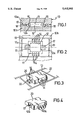
- FIG. 1 is a cross-sectional view through a portion of the mold according to the invention.
- FIG. 2 is a plan view of the lower plate of the mold shown in FIG. 1;
- FIG. 3 is a perspective view of a semiconductor device structure as it appears directly after molding
- FIG. 4 is a perspective view of a finished semiconductor device structure as obtained using the mold and method of this invention.
- a mold generally denoted by 10, comprises two superimposable plates or halves 10a and 10b.
- the two half-molds when superimposed on each other, will delimit on their interiors hollows which are connected to an inlet by suitable channels, not shown.
- a resin material such as a thermosetting epoxy resin, in a liquefied state can be injected into the hollows under pressure to fill them.
- FIG. 1 Shown in FIG. 1 is a mold portion having a hollow 11 formed of two compartments correspondingly provided in the two mold halves.
- a blank piece comprising a metal plate 12, a chip of a semiconductor material attached to the plate, and a framework 13 of leads 14 electrically connected to the chip is placed into the lower compartment.
- the drawing FIGS. 1 and 2 only show the metal plate 12 and the framework 13. It can be seen that the plate 12 is formed of a broad portion, rectangular in shape, and two wings 12a which extend from the small sides of the rectangle and are slightly sunk with respect to the top surface of the plate.
- the upper mold half 10a has two pusher elements 16 which, with the mold closed and the blank piece placed within the hollow, engage surface areas 17 of the plate with their free ends so as to hold it pressed against the hollow bottom.
- the lower compartment of the hollow 11 extends sideways into two recesses 18 which, with the plate 12 inserted into its socket in the lower mold half 10b, are covered by the thickness of the wings 12a, specifically by the side surfaces of their end edges, extend inside the lower mold half, and are covered at the top by a flat portion of the upper mold half 10a. They are also communicated to the resin inlet by channels, not shown.
- a structure like that shown in FIG. 3 is taken out of the mold. It consists of a solidified resin body 20 whence the metal strips 14 of the device terminal leads protrude (still held together by the framework 13). The body 20 encapsulates the plate 12 to leave free only its bottom surface (not shown in the drawing). This bottom surface was held in contact with the bottom of the hollow during the molding process.
- the structure also has two projections 22, formed by resin which flowed into the recesses 18.These projections joined to the remainder of the structure only along the edges of the wings 12a of the metal plate 12. According to the invention, these are then separated from the remainder of the structure using a suitable tool. This is not a precision operation: the projections are simply hit centrally with a punch to knock them off.
- the dimensions of a sample embodiment include: plastics body 20: 11 ⁇ 16 ⁇ 3.2 mm; heat sink plate (not including wings 12a): 7 ⁇ 13.5 ⁇ 1.2 mm; wings 12a: 1.2 ⁇ 2.8 ⁇ 1 mm thick.
- the mold and method of this invention provide a device which is readyfor surface mounting with no post-machining apart from the simple separation of the projections 22.
- the surface of the heat sink is free of any traces of resin from seepage due to the elements 16 being pressed against the plate 12, and the edges of the latter are (within the span of the wings) completely free of resin. Notice that the thickness of the wings 12a is reduced, conveniently, from that of the remainder of the plate 12 to both facilitate separation of the projections 22 and improve the mechanical anchoring of the resin body 20 on the plate 12.
- the pusher elements 16 could be constructed such that the surfaces 17 of the plate contacting them have shapes and dimensions other than those shown, and as a result, the wings 12a also have shapes and breadths other than those shown, it being possible, in the extreme, to extend them to span thefull width of the plate 12.
Abstract
A mold is disclosed for semiconductor devices intended for surface mounting, being of a type which comprises a metal plate and a body of solidified plastic resin. It consists of two plates which delimit at least one hollow adapted to receive the plate and to contain resin for forming the device body. Two elements of the mold push the plate from opposed sides against the bottom of the hollow. The hollow has two side extensions which are delimited by the side surfaces of the plate edges, thereby solidified projections are formed thereon which separate readily after the molding process. Thus, a structure is obtained wherein the plate has its bottom surface and two side edge portions fully exposed to allow optimum and controllable soldering to a printed circuit board.
Description
This invention relates to the manufacture of semiconductor electronic devices, and mote particularly, to a mold and a method for manufacturing a semiconductor device structure intended for surface mounting and being of a type which comprises a metal plate and a plastic (solidified resin) body joined to each other.
As is known, integrated circuits and other active electronic devices or components are built up on chips of a semiconductor material having a surface area on the order of a few square millimeters, and require for their connection to an external electric circuit special supporting, enclosing and electric interconnection structures. A typical structure suited for the purpose basically comprises a solid resin body enclosing a chip which is connected, by thin wires soldered to metallized regions specially provided on its surface, to corresponding electric conductors or terminal leads led out of the polymer body. With power integrated circuits, that is devices designed to operate on high currents, and therefore, liable to become heated to a significant extent, such structures also comprise a small metal plate through which a chip mounted thereon can transfer the heat generated during its operation to the environment.
In manufacturing the last-mentioned structures, the plate is blanked from sheet metal, e.g. copper; thereafter, a chip is secured on the metal plate either by soldering with a low-melt alloy such as a lead-tin alloy, or by cementing with a suitable adhesive such as an epoxy adhesive; a set of metal strips, intended to become the terminal leads for the device, are then blanked off thin sheet metal but still left joined to one another by interconnecting sections, and mounted to the plate in an electrically insulated manner therefrom; thin wires, usually of gold, are soldered, on the one side, to the metallized regions of the chip using a low-melt alloy, and on the other side, welded to the ends of the metal strips using a so-called "thermosonic" process wherein heat and ultrasound are applied simultaneously; thereafter, the assembly is placed into a specially provided mold, into which a material such as a thermosetting epoxy resin is then introduced in a liquefied state; on curing the resin, a structure is obtained which comprises a solidified resign body encapsulating the above-described elements excepting for one face of the metal plate and part of the metal strips, i.e. of the device terminal leads, and their interconnecting sections; the latter are then removed, along with any interconnecting sections present, as by blanking to yield the finished electronic product.
With devices intended for surface mounting, that is for attachment to a printed circuit board by welding the heat sink and the lead ends to specially arranged metal regions, all located on the same board surface, the leads are bent to have their free ends all lying in the plane which contains the exposed side of the heat sink. The soldering is performed by applying a low-melt solder layer onto the metal regions of the board and then arranging the circuit components on the board with their respective terminals, and in the instance of devices of the kind described above, with the exposed side of the heat sink, in contact with the metal regions, and by heating the board to melt the solder layers and thereby have the terminals and heat sinks soldered on cooling to their respective metal regions.
The soldered joint quality is then inspected for appearance and shape. With semiconductor devices which incorporate a heat sink, this inspection cannot be carried out (or can be carried out only imperfectly) because the border line between the heat sink and the solder are concealed from view. Further, checking that the heat sink is correctly aligned to the corresponding printed circuit area also becomes more difficult due to that border line being hidden from view.
To obviate such drawbacks, structures have been proposed wherein the metal plate of the heat sink has exposed edges on two opposed sides of the structure. To make such structures, however, a special, critical and troublesome, additional machining step is required to rid such opposed edges of the solidified resin that forms all around the plate during the molding process.
Another machining step which becomes usually necessary to prepare such structures for soldering is the removal of thin polymer layers which form on the outward side of the heat sink due to seepage during the molding process. To prevent such seepage, there are known molds having shaped interiors to present elements for pushing the metal plate against the bottom of the hollow wherein the solidified resin body of the structure is to be formed.
It is the object of this invention to provide a method for manufacturing packaged device structures without post-machining to remove solidified resin that has seeped onto the heat sink nor any other troublesome machining to remove solidified resin from the heat sink edges.
The present application provides a manufacturing method, for packaging integrated circuits, in which the back of the heat sink plate is left substantially free of solidified resin. Moreover, a clean metal surface is easily achieved at the edge of the heat sink plate. Note that this clean metal surface is adjacent to a relief in the solidified resin encapsulation body. Thus, the quality of the solder joint can easily be inspected at this location.
In the presently preferred embodiment, this is achieved using a mold which includes two plates which delimit at least one hollow adapted to receive the plate and to contain resin for forming the device body. Two elements of the mold push the down, at opposite ends of the top surface of the plate, to hold the plate against the bottom of the hollow. The hollow has two side extensions which are delimited by the side surfaces of the plate edges, thereby solidified resin projections are formed thereon which separate readily after the molding process. Thus, a structure is obtained wherein the plate has its bottom surface and two side edge portions fully exposed to allow optimum and controllable soldering to a printed circuit board.
The present invention will be described with reference to the accompanying drawings, which show important sample embodiments of the invention and which are incorporated in the specification hereof by reference, wherein:
FIG. 1 is a cross-sectional view through a portion of the mold according to the invention;
FIG. 2 is a plan view of the lower plate of the mold shown in FIG. 1;
FIG. 3 is a perspective view of a semiconductor device structure as it appears directly after molding; and
FIG. 4 is a perspective view of a finished semiconductor device structure as obtained using the mold and method of this invention.
The numerous innovative teachings of the present application will be described with particular reference to the presently preferred embodiment.However, it should be understood that this class of embodiments provides only a few examples of the many advantageous uses of the innovative teachings herein. In general, statements made in the specification of the present application do not necessarily delimit any of the various claimed inventions. Moreover, some statements may apply to some inventive featuresbut not to others.
With particular reference to FIGS. 1 and 2, a mold, generally denoted by 10, comprises two superimposable plates or halves 10a and 10b. The two half-molds, when superimposed on each other, will delimit on their interiors hollows which are connected to an inlet by suitable channels, not shown. Through these channels, a resin material, such as a thermosetting epoxy resin, in a liquefied state can be injected into the hollows under pressure to fill them.
Shown in FIG. 1 is a mold portion having a hollow 11 formed of two compartments correspondingly provided in the two mold halves. A blank piece comprising a metal plate 12, a chip of a semiconductor material attached to the plate, and a framework 13 of leads 14 electrically connected to the chip is placed into the lower compartment. In the interest of simplicity, the drawing FIGS. 1 and 2 only show the metal plate 12 and the framework 13. It can be seen that the plate 12 is formed of a broad portion, rectangular in shape, and two wings 12a which extend from the small sides of the rectangle and are slightly sunk with respect to the top surface of the plate.
The upper mold half 10a has two pusher elements 16 which, with the mold closed and the blank piece placed within the hollow, engage surface areas 17 of the plate with their free ends so as to hold it pressed against the hollow bottom.
The lower compartment of the hollow 11 extends sideways into two recesses 18 which, with the plate 12 inserted into its socket in the lower mold half 10b, are covered by the thickness of the wings 12a, specifically by the side surfaces of their end edges, extend inside the lower mold half, and are covered at the top by a flat portion of the upper mold half 10a. They are also communicated to the resin inlet by channels, not shown.
As the resin is injected into the mold in a liquefied state, it fills the hollow completely, including its side extensions 18. After curing, a structure like that shown in FIG. 3 is taken out of the mold. It consists of a solidified resin body 20 whence the metal strips 14 of the device terminal leads protrude (still held together by the framework 13). The body 20 encapsulates the plate 12 to leave free only its bottom surface (not shown in the drawing). This bottom surface was held in contact with the bottom of the hollow during the molding process. The structure also has two projections 22, formed by resin which flowed into the recesses 18.These projections joined to the remainder of the structure only along the edges of the wings 12a of the metal plate 12. According to the invention, these are then separated from the remainder of the structure using a suitable tool. This is not a precision operation: the projections are simply hit centrally with a punch to knock them off.
The dimensions of a sample embodiment include: plastics body 20: 11×16×3.2 mm; heat sink plate (not including wings 12a): 7×13.5×1.2 mm; wings 12a: 1.2×2.8×1 mm thick.
Thereafter, the sections of framework 13, which had been holding the leads together, are shorn off. Finally, the leads are bent over as shown in FIG.4 so that their end portions will lie in the bottom plane of the structure.The packaged device is now ready to be soldered to a surface of a printed circuit board.
Thus, the mold and method of this invention provide a device which is readyfor surface mounting with no post-machining apart from the simple separation of the projections 22. The surface of the heat sink is free of any traces of resin from seepage due to the elements 16 being pressed against the plate 12, and the edges of the latter are (within the span of the wings) completely free of resin. Notice that the thickness of the wings 12a is reduced, conveniently, from that of the remainder of the plate 12 to both facilitate separation of the projections 22 and improve the mechanical anchoring of the resin body 20 on the plate 12.
Further Modifications and Variations
It will be recognized by those skilled in the art that the innovative concepts disclosed in the present application can be applied in a wide variety of contexts. Moreover, the preferred implementation can be modified in a tremendous variety of ways. Accordingly, it should be understood that the modifications and variations suggested below and aboveare merely illustrative. These examples may help to show some of the scope of the inventive concepts, but these examples do not nearly exhaust the full scope of variations in the disclosed novel concepts.
While a single embodiment of the invention has been described and illustrated, it is understood that many variations and modifications are possible within the same overall inventive concept. AS an example, the pusher elements 16 could be constructed such that the surfaces 17 of the plate contacting them have shapes and dimensions other than those shown, and as a result, the wings 12a also have shapes and breadths other than those shown, it being possible, in the extreme, to extend them to span thefull width of the plate 12.
As will be recognized by those skilled in the art, the innovative concepts described in the present application can be modified and varied over a tremendous range of applications, and accordingly the scope of patented subject matter is not limited by any of the specific exemplary teachings given.
Claims (20)
1. A method for manufacturing packaged integrated circuit devices, comprising the steps of:
(a.) providing a heat sink plate;
(b.) affixing an integrated circuit to a first surface of said heat sink plate;
(c.) bonding said integrated circuit to multiple leads of a lead frame;
(d.) placing said heat sink plate, said integrated circuit, and portions of said leads within a mold, and closing said mold;
(i.) wherein said mold includes multiple pushing elements which press against known locations of said first surface of said plate at opposite ends thereof when said mold is closed;
(ii.) wherein said mold further includes cavities adjacent to said known locations at opposite ends of said plate;
(e.) injecting resin into said mold, and thereby forming a body encapsulating said integrated circuit, and also thereby forming projections adhering to edges of said plate adjacent to said known locations; and
(f.) trimming said projections from the edges of said plate, to leave clean metal surfaces exposed.
2. The method of claim 1, further comprising the additional step, after said step (e.), of trimming off outer portions of said lead frame, to leave multiple ones of said leads electrically separate.
3. The method of claim 1, wherein, during said step of emplacing said lead frame, said lead frame is mechanically attached to said plate.
4. The method of claim 1, wherein multiple linked ones of said lead frames are simultaneously emplaced onto multiple ones of said molds.
5. The method of claim 1, wherein multiple linked ones of said heat sink plates are simultaneously emplaced onto multiple ones of said molds.
6. The method of claim 1, further comprising the additional step of curing said resin to form a durable solid material.
7. A method for manufacturing packaged integrated circuit devices, comprising the steps of:
(a.) providing a metal heat sink plate;
(b.) soldering a semiconductor integrated circuit to a first surface of said metal heat sink plate;
(c.) electrically connecting said integrated circuit to multiple leads of a lead frame;
(d.) emplacing said metal heat sink plate, said integrated circuit, and portions of said leads within a mold, and closing said mold;
(i.) wherein said mold includes multiple pushing elements which press against multiple known locations of said first surface of said metal heat sink plate when said mold is closed;
(ii.) wherein said mold further includes cavities adjacent to the edge of said metal heat sink plate, in proximity to said known locations;
(e.) injecting resin into said mold, and thereby forming a body encapsulating said integrated circuit, and also thereby forming projections adhering to edges of said metal heat sink plate adjacent to said known locations; and
(f.) trimming said projections from the edges of said metal heat sink plate, to leave clean metal surfaces exposed.
8. The method of claim 7, further comprising the additional step, after said step (e.), of trimming off outer portions of said lead frame, to leave multiple ones of said leads electrically separate.
9. The method of claim 7, wherein, during said step of emplacing said lead frame, said lead frame is mechanically attached to said plate.
10. The method of claim 7, wherein multiple linked ones of said lead frames are simultaneously emplaced onto multiple ones of said molds.
11. The method of claim 7, wherein multiple linked ones of said heat sink plates are simultaneously emplaced onto multiple ones of said molds.
12. The method of claim 7, further comprising the additional step of curing said resin to form a durable solid material.
13. A method for manufacturing packaged integrated circuit devices, comprising the steps of:
(a.) providing a metal heat sink plate;
(b.) affixing a first surface of a semiconductor integrated circuit to a first surface of said metal heat sink plate;
(c.) placing a lead frame in proximity to and surrounding said integrated circuit, and forming wire connections from multiple contact pads on a first surface of integrated circuit to multiple leads of said lead frame;
(d.) emplacing said metal heat sink plate, said integrated circuit, and portions of said leads in a mold, and closing said mold;
(i.) wherein said mold includes one or more pushing elements which press against multiple known locations of said first surface of said metal heat sink plate;
(ii.) wherein said mold further includes one or more cavities laterally adjacent to the edge of said metal heat sink plate, each in proximity to a respective one of said known locations;
(e.) injecting resin into said mold, and thereby forming a body encapsulating said integrated circuit, and also thereby forming projections adhering to edges of said metal heat sink plate adjacent to said known locations; and
(f.) trimming said projections from the edges of said metal heat sink plate, to leave clean metal surfaces exposed.
14. The method of claim 13, further comprising the additional step, after said step (e.), of trimming off outer portions of said lead frame, to leave multiple ones of said leads electrically separate.
15. The method of claim 13, wherein, during said step of emplacing said lead frame, said lead frame is mechanically attached to said plate.
16. The method of claim 13, wherein multiple linked ones of said lead frames are simultaneously emplaced onto multiple ones of said molds.
17. The method of claim 13, wherein multiple linked ones of said heat sink plates are simultaneously emplaced onto multiple ones of said molds.
18. The method of claim 13, further comprising the additional step of curing said resin to form a durable solid material.
19. A method for manufacturing a semiconductor electronic device structure comprising a metal plate having first and second flat surfaces and an electronic device mounted on said second surface and a solidified resin body which encapsulates the plate while leaving said first flat surface exposed, comprising the steps of:
introducing said metal plate into a hollow of a mold which includes two superimposable plates jointly delimiting said hollow, and
wherein said hollow is adapted to receive said metal plate with said first flat surface held in contact with a bottom wall of said hollow and to contain a sufficient amount of resin to form said body, and
wherein said mold includes means to push said metal plate against said bottom wall while engaging one or more surface areas thereof delimited by said second flat surface,
wherein one or more portions of said hollow define extension(s) which, with the mold closed and the plate inserted into said hollow, are delimited by the lateral surface of said plate side and the inner walls of said mold;
injecting resin, in a liquefied state, into said hollow;
curing the resin; and
taking out of the mold a device consisting of said metal plate and the solidified resin body resulting from the preceding steps; and
removing the portion(s) of polymer formed in said extension(s) of said hollow while separating them from their respective side surfaces of said plate.
20. A method according to claim 19, characterized in that the blank Piece is obtained from a substantially quadrilateral-shaped metal plate having two wings which extend from two opposed sides, the end sides of such wings defining said side surfaces of the plate.
Applications Claiming Priority (2)
| Application Number | Priority Date | Filing Date | Title |
|---|---|---|---|
| ITMI91A3440 | 1991-12-20 | ||
| ITMI913440A IT1252575B (en) | 1991-12-20 | 1991-12-20 | MOLD AND PROCESS FOR THE MANUFACTURE OF SEMICONDUCTOR PLASTIC DEVICES, WITH VISIBLE METALLIC DISSIPATOR FOR WELDING CONTROL |
Publications (1)
| Publication Number | Publication Date |
|---|---|
| US5445995A true US5445995A (en) | 1995-08-29 |
Family
ID=11361402
Family Applications (1)
| Application Number | Title | Priority Date | Filing Date |
|---|---|---|---|
| US07/994,421 Expired - Lifetime US5445995A (en) | 1991-12-20 | 1992-12-21 | Method for manufacturing plastic-encapsulated semiconductor devices with exposed metal heat sink |
Country Status (5)
| Country | Link |
|---|---|
| US (1) | US5445995A (en) |
| EP (1) | EP0548496B1 (en) |
| JP (1) | JP3217876B2 (en) |
| DE (1) | DE69216377T2 (en) |
| IT (1) | IT1252575B (en) |
Cited By (6)
| Publication number | Priority date | Publication date | Assignee | Title |
|---|---|---|---|---|
| EP0845801A1 (en) * | 1996-11-27 | 1998-06-03 | STMicroelectronics S.r.l. | Process for manufacturing a plastic package for electronic devices having an heat dissipator |
| US5852324A (en) * | 1996-01-25 | 1998-12-22 | Sgs-Thomson Microelectronics S.R.L. | Plastic body surface-mounting semiconductor power device having dimensional characteristics optimized for use of standard shipping and testing modes |
| US5939775A (en) * | 1996-11-05 | 1999-08-17 | Gcb Technologies, Llc | Leadframe structure and process for packaging intergrated circuits |
| US6046501A (en) * | 1996-10-02 | 2000-04-04 | Matsushita Electric Industrial Co., Ltd. | RF-driven semiconductor device |
| US6175150B1 (en) * | 1997-04-17 | 2001-01-16 | Nec Corporation | Plastic-encapsulated semiconductor device and fabrication method thereof |
| US20050231925A1 (en) * | 2004-04-14 | 2005-10-20 | Denso Corporation | Semiconductor device and method for manufacturing the same |
Families Citing this family (5)
| Publication number | Priority date | Publication date | Assignee | Title |
|---|---|---|---|---|
| IT1252575B (en) * | 1991-12-20 | 1995-06-19 | Sgs Thomson Microelectronics | MOLD AND PROCESS FOR THE MANUFACTURE OF SEMICONDUCTOR PLASTIC DEVICES, WITH VISIBLE METALLIC DISSIPATOR FOR WELDING CONTROL |
| DE19624478A1 (en) * | 1996-02-08 | 1998-01-02 | Bayerische Motoren Werke Ag | Method of manufacturing an electronic control device |
| DE19621766A1 (en) * | 1996-05-30 | 1997-12-04 | Siemens Ag | Semiconductor arrangement with plastic housing and heat spreader |
| WO2002020236A2 (en) * | 2000-09-08 | 2002-03-14 | Asm Technology Singapore Pte Ltd. | A mold |
| US20040113240A1 (en) | 2002-10-11 | 2004-06-17 | Wolfgang Hauser | An electronic component with a leadframe |
Citations (14)
| Publication number | Priority date | Publication date | Assignee | Title |
|---|---|---|---|---|
| DE2900114A1 (en) * | 1978-08-07 | 1980-02-14 | Dai Ichi Seiko Co Ltd | Encapsulating semiconductor devices with plastic - where device has heat sealing plate in a recess which is either sealed or has grooves to allow easy removal of hardened plastic (NL 11.2.80) |
| US4216577A (en) * | 1975-12-31 | 1980-08-12 | Compagnie Internationale Pour L'informatique Cii-Honeywell Bull (Societe Anonyme) | Portable standardized card adapted to provide access to a system for processing electrical signals and a method of manufacturing such a card |
| JPS6188535A (en) * | 1984-10-08 | 1986-05-06 | Nec Corp | Manufacture of semiconductor device |
| JPS62128721A (en) * | 1985-11-29 | 1987-06-11 | Rohm Co Ltd | Molding of resin |
| US4688152A (en) * | 1986-08-11 | 1987-08-18 | National Semiconductor Corporation | Molded pin grid array package GPT |
| US4822550A (en) * | 1986-04-17 | 1989-04-18 | Citizen Watch Co., Ltd. | Method of molding a protective cover on a pin grid array |
| US4887149A (en) * | 1986-07-17 | 1989-12-12 | Sgs Microelectronica S.P.A. | Semiconductor device mounted in a highly flexible, segmented package, provided with heat sink |
| JPH02184040A (en) * | 1989-01-11 | 1990-07-18 | Nec Corp | Manufacture of semiconductor device |
| US4951124A (en) * | 1986-10-24 | 1990-08-21 | Kabushiki Kaisha Toshiba | Semiconductor device |
| US4963975A (en) * | 1987-09-26 | 1990-10-16 | Kabushiki Kaisha Toshiba | Semiconductor device |
| US5091341A (en) * | 1989-05-22 | 1992-02-25 | Kabushiki Kaisha Toshiba | Method of sealing semiconductor device with resin by pressing a lead frame to a heat sink using an upper mold pressure member |
| US5157478A (en) * | 1989-04-19 | 1992-10-20 | Mitsubishi Denki Kabushiki Kaisha | Tape automated bonding packaged semiconductor device incorporating a heat sink |
| EP0548496A1 (en) * | 1991-12-20 | 1993-06-30 | STMicroelectronics S.r.l. | A mold and a method for manufacturing semiconductor devices of plastics incorporating an exposed heat sink of metal for inspecting the soldered joint |
| US5291178A (en) * | 1991-04-10 | 1994-03-01 | Caddock Electronics, Inc. | Film-type resistor assembly with full encapsulation except at the bottom surface |
-
1991
- 1991-12-20 IT ITMI913440A patent/IT1252575B/en active IP Right Grant
-
1992
- 1992-10-22 EP EP92118078A patent/EP0548496B1/en not_active Expired - Lifetime
- 1992-10-22 DE DE69216377T patent/DE69216377T2/en not_active Expired - Fee Related
- 1992-11-06 JP JP29671592A patent/JP3217876B2/en not_active Expired - Lifetime
- 1992-12-21 US US07/994,421 patent/US5445995A/en not_active Expired - Lifetime
Patent Citations (15)
| Publication number | Priority date | Publication date | Assignee | Title |
|---|---|---|---|---|
| US4216577A (en) * | 1975-12-31 | 1980-08-12 | Compagnie Internationale Pour L'informatique Cii-Honeywell Bull (Societe Anonyme) | Portable standardized card adapted to provide access to a system for processing electrical signals and a method of manufacturing such a card |
| DE2900114A1 (en) * | 1978-08-07 | 1980-02-14 | Dai Ichi Seiko Co Ltd | Encapsulating semiconductor devices with plastic - where device has heat sealing plate in a recess which is either sealed or has grooves to allow easy removal of hardened plastic (NL 11.2.80) |
| JPS6188535A (en) * | 1984-10-08 | 1986-05-06 | Nec Corp | Manufacture of semiconductor device |
| JPS62128721A (en) * | 1985-11-29 | 1987-06-11 | Rohm Co Ltd | Molding of resin |
| US4822550A (en) * | 1986-04-17 | 1989-04-18 | Citizen Watch Co., Ltd. | Method of molding a protective cover on a pin grid array |
| US4887149A (en) * | 1986-07-17 | 1989-12-12 | Sgs Microelectronica S.P.A. | Semiconductor device mounted in a highly flexible, segmented package, provided with heat sink |
| US4688152A (en) * | 1986-08-11 | 1987-08-18 | National Semiconductor Corporation | Molded pin grid array package GPT |
| US4951124A (en) * | 1986-10-24 | 1990-08-21 | Kabushiki Kaisha Toshiba | Semiconductor device |
| US4963975A (en) * | 1987-09-26 | 1990-10-16 | Kabushiki Kaisha Toshiba | Semiconductor device |
| JPH02184040A (en) * | 1989-01-11 | 1990-07-18 | Nec Corp | Manufacture of semiconductor device |
| US5157478A (en) * | 1989-04-19 | 1992-10-20 | Mitsubishi Denki Kabushiki Kaisha | Tape automated bonding packaged semiconductor device incorporating a heat sink |
| US5091341A (en) * | 1989-05-22 | 1992-02-25 | Kabushiki Kaisha Toshiba | Method of sealing semiconductor device with resin by pressing a lead frame to a heat sink using an upper mold pressure member |
| US5291178A (en) * | 1991-04-10 | 1994-03-01 | Caddock Electronics, Inc. | Film-type resistor assembly with full encapsulation except at the bottom surface |
| EP0548496A1 (en) * | 1991-12-20 | 1993-06-30 | STMicroelectronics S.r.l. | A mold and a method for manufacturing semiconductor devices of plastics incorporating an exposed heat sink of metal for inspecting the soldered joint |
| JPH05326589A (en) * | 1991-12-20 | 1993-12-10 | Sgs Thomson Microelettronica Spa | Mold for fabricating semiconductor electronic element structure and manufacture of semiconductor electronic element structure using above described mold |
Non-Patent Citations (2)
| Title |
|---|
| Patent Abstracts of Japan, vol. 015, No. 098 (E 1042) 8 Mar. 1991. * |
| Patent Abstracts of Japan, vol. 015, No. 098 (E-1042) 8 Mar. 1991. |
Cited By (10)
| Publication number | Priority date | Publication date | Assignee | Title |
|---|---|---|---|---|
| US5852324A (en) * | 1996-01-25 | 1998-12-22 | Sgs-Thomson Microelectronics S.R.L. | Plastic body surface-mounting semiconductor power device having dimensional characteristics optimized for use of standard shipping and testing modes |
| US6046501A (en) * | 1996-10-02 | 2000-04-04 | Matsushita Electric Industrial Co., Ltd. | RF-driven semiconductor device |
| US5939775A (en) * | 1996-11-05 | 1999-08-17 | Gcb Technologies, Llc | Leadframe structure and process for packaging intergrated circuits |
| EP0845801A1 (en) * | 1996-11-27 | 1998-06-03 | STMicroelectronics S.r.l. | Process for manufacturing a plastic package for electronic devices having an heat dissipator |
| US5953593A (en) * | 1996-11-27 | 1999-09-14 | Stmicroelectronics S.R.L. | Method and mold for manufacturing a plastic package for an electronic device having a heat sink |
| US6175150B1 (en) * | 1997-04-17 | 2001-01-16 | Nec Corporation | Plastic-encapsulated semiconductor device and fabrication method thereof |
| US20050231925A1 (en) * | 2004-04-14 | 2005-10-20 | Denso Corporation | Semiconductor device and method for manufacturing the same |
| US7843700B2 (en) | 2004-04-14 | 2010-11-30 | Denso Corporation | Semiconductor device |
| US20110044009A1 (en) * | 2004-04-14 | 2011-02-24 | Denso Corporation | Semiconductor device |
| US8179688B2 (en) | 2004-04-14 | 2012-05-15 | Denso Corporation | Semiconductor device |
Also Published As
| Publication number | Publication date |
|---|---|
| DE69216377T2 (en) | 1997-04-24 |
| DE69216377D1 (en) | 1997-02-13 |
| EP0548496A1 (en) | 1993-06-30 |
| ITMI913440A0 (en) | 1991-12-20 |
| EP0548496B1 (en) | 1997-01-02 |
| JPH05326589A (en) | 1993-12-10 |
| JP3217876B2 (en) | 2001-10-15 |
| IT1252575B (en) | 1995-06-19 |
| ITMI913440A1 (en) | 1993-06-20 |
Similar Documents
| Publication | Publication Date | Title |
|---|---|---|
| US3930114A (en) | Integrated circuit package utilizing novel heat sink structure | |
| US4079511A (en) | Method for packaging hermetically sealed integrated circuit chips on lead frames | |
| US5808359A (en) | Semiconductor device having a heat sink with bumpers for protecting outer leads | |
| US5072283A (en) | Pre-formed chip carrier cavity package | |
| KR100190981B1 (en) | Method of manufacturing one side resin sealing type semiconductor devices | |
| US5652461A (en) | Semiconductor device with a convex heat sink | |
| US6989121B2 (en) | Method for encasing plastic array packages | |
| US5262927A (en) | Partially-molded, PCB chip carrier package | |
| US7011251B1 (en) | Die down multi-media card and method of making same | |
| JPH08306853A (en) | Semiconductor device, manufacture thereof and manufacture of lead frame | |
| JPS60227457A (en) | Integrated circuit package | |
| JPH02122557A (en) | Pin lattice array integrated circuit package | |
| US5370517A (en) | Apparatus for assembling and resin-encapsulating a heat sink-mounted semiconductor power device | |
| US5445995A (en) | Method for manufacturing plastic-encapsulated semiconductor devices with exposed metal heat sink | |
| KR19980054919A (en) | Printed circuit board for ball grid array (BGA) semiconductor package with through hole for degating and molding method of ball grid array semiconductor package using same | |
| US4084312A (en) | Electrically isolated heat sink lead frame for plastic encapsulated semiconductor assemblies | |
| US6541856B2 (en) | Thermally enhanced high density semiconductor package | |
| JP2005191146A (en) | Method of manufacturing hybrid integrated circuit device | |
| US6858474B1 (en) | Wire bond package and packaging method | |
| KR20050065328A (en) | Hybrid integrated circuits device and their fabricating method thereof | |
| JPH0936155A (en) | Manufacture of semiconductor device | |
| JPH0870082A (en) | Semiconductor integrated circuit device and its manufacture, and lead frame | |
| EP1028464A1 (en) | Semiconductor device with improved interconnections between the chip and the terminals, and process for its manufacture | |
| JP3813680B2 (en) | Manufacturing method of semiconductor device | |
| KR200328473Y1 (en) | BGA Semiconductor Package |
Legal Events
| Date | Code | Title | Description |
|---|---|---|---|
| AS | Assignment |
Owner name: SGS-THOMSON MICROELECTRONICS, S.R.L., ITALY Free format text: ASSIGNMENT OF ASSIGNORS INTEREST.;ASSIGNORS:CASATI, PAOLD;MAGNI, PIERANGELO;REEL/FRAME:006483/0983 Effective date: 19930216 |
|
| STCF | Information on status: patent grant |
Free format text: PATENTED CASE |
|
| FPAY | Fee payment |
Year of fee payment: 4 |
|
| FPAY | Fee payment |
Year of fee payment: 8 |
|
| FEPP | Fee payment procedure |
Free format text: PAYOR NUMBER ASSIGNED (ORIGINAL EVENT CODE: ASPN); ENTITY STATUS OF PATENT OWNER: LARGE ENTITY |
|
| FPAY | Fee payment |
Year of fee payment: 12 |