US5432128A - Reliability enhancement of aluminum interconnects by reacting aluminum leads with a strengthening gas - Google Patents
Reliability enhancement of aluminum interconnects by reacting aluminum leads with a strengthening gas Download PDFInfo
- Publication number
- US5432128A US5432128A US08/250,062 US25006294A US5432128A US 5432128 A US5432128 A US 5432128A US 25006294 A US25006294 A US 25006294A US 5432128 A US5432128 A US 5432128A
- Authority
- US
- United States
- Prior art keywords
- aluminum
- leads
- strengthened
- aluminum leads
- layer
- Prior art date
- Legal status (The legal status is an assumption and is not a legal conclusion. Google has not performed a legal analysis and makes no representation as to the accuracy of the status listed.)
- Expired - Lifetime
Links
Images


Classifications
-
- H—ELECTRICITY
- H01—ELECTRIC ELEMENTS
- H01L—SEMICONDUCTOR DEVICES NOT COVERED BY CLASS H10
- H01L21/00—Processes or apparatus adapted for the manufacture or treatment of semiconductor or solid state devices or of parts thereof
- H01L21/70—Manufacture or treatment of devices consisting of a plurality of solid state components formed in or on a common substrate or of parts thereof; Manufacture of integrated circuit devices or of parts thereof
- H01L21/71—Manufacture of specific parts of devices defined in group H01L21/70
- H01L21/768—Applying interconnections to be used for carrying current between separate components within a device comprising conductors and dielectrics
- H01L21/76838—Applying interconnections to be used for carrying current between separate components within a device comprising conductors and dielectrics characterised by the formation and the after-treatment of the conductors
Definitions
- This invention relates generally to the fabrication of semiconductor devices, and more specifically to semiconductors with submicron spacing between aluminum leads and low-dielectric constant materials.
- Semiconductors are widely used in integrated circuits for electronic applications, including radios and televisions. Such integrated circuits typically use multiple transistors fabricated in single crystal silicon. Many integrated circuits now contain multiple levels of metallization for interconnections. Semi-conductor devices are being scaled in the horizontal dimension to reduce wafer cost by obtaining more chips per wafer or by increasing circuit complexity, getting more transistors per chip.
- metal leads are not necessarily being scaled in the vertical dimension. The reason for this is that as metal leads are scaled in the horizontal direction, the current density of the leads increases. If the metal leads were also scaled in the vertical dimension, the current density would exceed reliability limits. With horizontal scaling, these tall metal leads are being packed closer and closer together, causing capacitive coupling between the leads to become the primary limitation to circuit speed.
- Low-dielectric constant materials are being investigated for use with closely-spaced metal leads, including organic SOG (spin-on glass), polyimides, amorphous teflon, aerogels, air gaps, or vacuum gaps. These materials typically do not have the mechanical strength of traditionally-used SiO 2 .
- a wafer may be exposed to wet processing and chemical-mechanical polishing (CMP), which impose high mechanical stress and KOH-based slurry during etching. The end result of these processing steps on a wafer without proper structural support can be device failures and decreased yields.
- CMP chemical-mechanical polishing
- Aluminum is commonly used for metallization layers in ULSI semiconductors.
- the combination of weak aluminum conductors surrounded by low-dielectric constant materials (having low structural strength) has herein been discovered to be a problem.
- the present invention solves this hereto unrecognized problem. While the low-dielectric constant materials cannot easily be strengthened, surprisingly, the aluminum leads can relatively easily be strengthened, using gaseous processing.
- the invention encompasses using a strengthening gas to react with aluminum leads to form a strengthened shell, which enhances the reliability of metallic interconnects on a semiconductor device having submicron spacing between aluminum leads and a low-dielectric constant material.
- the invention may involve depositing an aluminum layer on a substrate, etching the aluminum layer in a predetermined pattern to form aluminum leads, exposing the aluminum leads to a strengthening gas to form a strengthened shell on the aluminum leads, and depositing a dielectric layer of a material having a dielectric constant less than 3 over the strengthened shell and the substrate.
- the strengthening gas may contain nitrogen, oxygen, or both.
- the exposing step may also comprise a rapid thermal anneal.
- An advantage of the invention is to mechanically strengthen the aluminum leads of a semiconductor wafer.
- it is an intrinsic operation, rather than extrinsic; the basic material required is already present on the wafer and is merely altered.
- FIGS. 1a to FIG. 1c are cross-sectional views of a semiconductor wafer, showing a preferred embodiment of the present invention.
- FIGS. 2a to 2c are cross-sectional views of a semiconductor wafer, showing another embodiment of the present invention.
- FIGS. 3a to 3f are cross-sectional views of a semiconductor wafer, showing the present invention and typical subsequent processing steps.
- FIGS. 4a to 4b are cross-sectional views of a semiconductor wafer, showing an alternate embodiment of the present invention.
- FIG. 1 is a cross-sectional view of a semiconductor wafer on which the present invention has been performed.
- FIG. 1a shows semiconductor wafer 10 with a substrate 12 which may, for example, contain transistors, diodes, and other semiconductor elements (not shown) as are well known in the art.
- the substrate 12 may also contain other metal interconnect layers.
- An aluminum interconnect layer has been deposited over substrate 12.
- the aluminum interconnect layer has been etched in a predetermined pattern to form etch lines, or aluminum leads 16. Some of the aluminum leads 16 are in close proximity to each other, e.g. less than one micrometer apart.
- the aluminum leads in ULSI technology are typically 0.1 to 0.8 micrometers apart, 0.1 to 0.8 micrometers in width, and have a height of 3 to 4 times the width (giving an aspect ratio of 3:1 to 4:1). It has been found that the tall, thin aluminum leads in ULSI technology are mechanically weak.
- FIG. 1b shows the wafer 10 after a strengthened shell 18 has been formed over aluminum leads 16.
- Strengthened shell 18 is thin and is preferably formed by exposing the aluminum leads 16 to a nitrogen-containing strengthening gas in order to react with the aluminum leads and form a strengthened shell. In the preferred embodiment, rapid thermal annealing is employed using NH 3 as the strengthening gas.
- the resultant strengthened shell 18 can be comprised of, for example, AlN, and is typically 40 to 50 ⁇ thick; approximately twice the thickness of a native oxide, which is generally 20 to 30 ⁇ .
- the aluminum leads 16 may be strengthened by exposure to an oxygen-containing gas, such as N 2 O, O 2 , or O 3 to form a strengthened shell 18 of Al 2 O 3 .
- dielectric layer 20 may then be deposited over strengthened shell 18 and substrate 12.
- the dielectric layer 20 of this invention is preferably comprised of a low-dielectric constant material, e.g. a dielectric material having a dielectric constant less than that of SiO 2 .
- the dielectric material shown in FIG. 1c is a viscous material that has left air gaps 22 adjacent the strengthening aluminum leads, whereby the air gaps provide a low dielectric medium between the closely-spaced aluminum leads 16.
- FIG. 2 is a cross-sectional view of a semiconductor wafer showing an alternate embodiment of the present invention.
- FIG. 2a shows semiconductor wafer 10 with a substrate 12.
- Insulating layer 14 has been deposited over the substrate 12 and preferably comprises SiO 2 .
- Insulating layer 14 could also comprise PETEOS (plasma-enhanced tetraethosiloxane), BPSG (boron phosphate silicate glass) or other dielectric materials.
- An aluminum interconnect layer has been deposited over insulating layer 14 and has been etched in a predetermined pattern to form aluminum leads 16.
- FIG. 2b shows the wafer 10 after a strengthened shell 18 has been formed over aluminum leads 16 by exposing the wafer to a strengthening gas.
- the strengthening gas may also react with the exposed portions of insulating layer 14 to form a strengthened insulating layer 19.
- the strengthened insulating layer 19 is thin, typically 40 to 50 ⁇ .
- dielectric layer 20 is deposited on strengthened shell 18 and strengthened insulating layer 19, as shown in FIG. 2c.
- the dielectric layer 20 shown in FIG. 2c is a low-dielectric constant material (rather than forming air gaps when applied; however, the material used for the first embodiment could also be used, leaving air gaps between closely-spaced aluminum leads and adjacent to aluminum leads).
- FIG. 3a shows the aluminum leads 16 with strengthened shell 18, formed as described for FIGS. 1 and 2.
- FIG. 3b shows the wafer after the dielectric layer 20 has been deposited. The dielectric layer 20 of the wafer 10 is then planarized typically by CMP as shown in FIG. 3c.
- the strengthened shell 18 strengthens the aluminum leads 16, so that the aluminum leads 16 can withstand the rigorous planarization step, and in addition, the strengthened shell 18 may be used as an etch stop.
- a CVD oxide layer 24 may be grown, and can be comprised, for example, of SiO 2 , as shown in FIG. 3d.
- a thick oxide layer 26 is deposited (FIG. 3e) and is preferably made of spin-on glass.
- the wafer may be patterned and etched to remove the thick oxide layer 26, the thin oxide layer 24, and the strengthened shell 18 in predetermined locations. These predetermined locations may create vias, such as via 27 shown in FIG. 3f, that is a hole to the first aluminum layer containing aluminum leads 16.
- a second aluminum layer 28 is deposited which fills via 27 to contact the aluminum leads 16 of the first aluminum layer.
- the present invention can be used on semiconductors using a variety of low-dielectric constant materials.
- low-dielectric constant materials such as pure polymers (e.g. parylene, teflon, polyimide) or organic spin-on glass (OSOG, e.g. silsequioxane and siloxane glass).
- pure polymers e.g. parylene, teflon, polyimide
- OSOG organic spin-on glass
- silsequioxane and siloxane glass organic spin-on glass
- U.S. Pat. No. 4,987,101 issued to Kaanta et al on Jan. 22, 1991 which describes a method for fabricating gas (air) dielectrics
- U.S. Pat. No. 5,103,288 issued to Sakamoto on Apr. 7, 1992 which describes a multilayered wiring structure which decreases capacitance by using a porous dielectric.
- the gas used to form the strengthened shell 18 may contain oxygen, nitrogen, or both.
- Table 2 shows some possible gases that can be used to form the strengthened shell 18 and the strengthened insulating layer 19. Other techniques may be used to form the strengthening shell, which must result in good conformality of the strengthened layers. The steps shown in FIG. 2 could also be applied to the substrate as shown in FIG. 1.
- FIG. 4 shows another possible embodiment of the invention.
- the aluminum leads 14 may have a native oxide 30 resident, from exposure to ambient oxygen (FIG. 4a). Exposure to NH 3 gas results in the formation of strengthened shell 18 beneath native oxide layer 30, as shown in FIG. 4b.
- the native oxide 30 may comprise AlO, which is in an unstable chemical state, since there am unpaired molecules (the stable chemical configuration is Al 2 O 3 ). Exposure to NH 3 may result in some bonding of N to the Al atoms in the native oxide 30, changing the composition of the native oxide 30 to AlON.
- the result of the invention is the mechanical strengthening of the aluminum leads 16.
- the novel method of applying a strengthened shell over aluminum leads to enhance reliability of the leads is beneficial to semiconductors having low-dielectric constant materials. Without first strengthening the aluminum leads with a strengthened shell, the aluminum leads can lack the mechanical strength required to yield a sufficient amount of functional devices per wafer. Low dielectric constant materials have been found to have low structural strength.
- One advantage of the present invention is to mechanically strengthen the aluminum leads of a semiconductor wafer.
- the mechanical properties of the strengthened shell are better than that of unstrengthened aluminum.
- AlN and Al 2 O 3 have melting temperatures above 2000° C., which is much higher than the melting of 660° C. for Al.
- the thermal conductivity of polycrystalline AlN, Al 2 O 3 and Si 3 N 4 used to form the strengthening layer is in the order of 30 W/mK at room temperature, which is one order of magnitude higher than SiO 2 .
- the thermal conductivity of AlN single crystal is as high as 260 W/mK.
- Si 3 N 4 formed by CVD has been used as a passivation layer in microelectronics applications because of its chemical stability, and diffusion barrier properties; and in addition, it has high mechanical strength. Therefore, mechanical benefits of forming the strengthened shell with the above chemistries are evident.
- Another advantage of the present invention is that it is an intrinsic operation, rather than extrinsic.
- the method involves exposing the wafer to a gas, rather than depositing a substance on the wafer.
- the basic material required is already present on the wafer; it is merely altered.
- the benefits of an intrinsic process include a cleaner operation than a deposition process, no additional material or layers added to the wafer, and ease of incorporating the process into a cluster tool.
- a cluster tool provides in situ transfer capability, which eliminates exposing the wafer to oxygen between steps.
Abstract
This invention encompasses using a strengthened shell to enhance reliability of aluminum leads of a semiconductor device. The invention includes depositing an aluminum layer on a substrate 12, etching the aluminum layer in a predetermined pattern to form aluminum leads 16, exposing the aluminum leads 16 to a strengthening gas to react and form a strengthened shell 18 on the aluminum leads 16, and depositing a dielectric layer 20 over the strengthened shell 18 and the substrate 12. The strengthening gas may contain nitrogen, oxygen, or both. The exposing step may also comprise a rapid thermal anneal, and the dielectric layer 20 is preferably comprised of a material having a dielectric constant of less than 3. An advantage of the invention is to mechanically strengthen the aluminum leads of a semiconductor wafer. In addition, it is an intrinsic operation, rather than extrinsic; the basic material required is already present on the wafer, it is merely altered.
Description
U.S. Patent Application, TI case T19068, entitled Method of Forming a Low Dielectric Constant Insulation in VLSI Applications, fried on Apr. 28, 1994 by Cho; and U.S. Patent Application, TI case T19109, entitled Suppression of Interlead Leakage When Using Air Gap Dielectric, fried concurrently with this application by Tigelaar et al.
This invention relates generally to the fabrication of semiconductor devices, and more specifically to semiconductors with submicron spacing between aluminum leads and low-dielectric constant materials.
Semiconductors are widely used in integrated circuits for electronic applications, including radios and televisions. Such integrated circuits typically use multiple transistors fabricated in single crystal silicon. Many integrated circuits now contain multiple levels of metallization for interconnections. Semi-conductor devices are being scaled in the horizontal dimension to reduce wafer cost by obtaining more chips per wafer or by increasing circuit complexity, getting more transistors per chip.
Although semiconductor devices are being scaled in the horizontal dimension to submicron (less than 1 micrometer) levels, metal leads are not necessarily being scaled in the vertical dimension. The reason for this is that as metal leads are scaled in the horizontal direction, the current density of the leads increases. If the metal leads were also scaled in the vertical dimension, the current density would exceed reliability limits. With horizontal scaling, these tall metal leads are being packed closer and closer together, causing capacitive coupling between the leads to become the primary limitation to circuit speed.
Low-dielectric constant materials are being investigated for use with closely-spaced metal leads, including organic SOG (spin-on glass), polyimides, amorphous teflon, aerogels, air gaps, or vacuum gaps. These materials typically do not have the mechanical strength of traditionally-used SiO2. During the fabrication of a device structure, a wafer may be exposed to wet processing and chemical-mechanical polishing (CMP), which impose high mechanical stress and KOH-based slurry during etching. The end result of these processing steps on a wafer without proper structural support can be device failures and decreased yields.
Aluminum is commonly used for metallization layers in ULSI semiconductors. The combination of weak aluminum conductors surrounded by low-dielectric constant materials (having low structural strength) has herein been discovered to be a problem.
The present invention solves this hereto unrecognized problem. While the low-dielectric constant materials cannot easily be strengthened, surprisingly, the aluminum leads can relatively easily be strengthened, using gaseous processing. The invention encompasses using a strengthening gas to react with aluminum leads to form a strengthened shell, which enhances the reliability of metallic interconnects on a semiconductor device having submicron spacing between aluminum leads and a low-dielectric constant material.
The invention may involve depositing an aluminum layer on a substrate, etching the aluminum layer in a predetermined pattern to form aluminum leads, exposing the aluminum leads to a strengthening gas to form a strengthened shell on the aluminum leads, and depositing a dielectric layer of a material having a dielectric constant less than 3 over the strengthened shell and the substrate. The strengthening gas may contain nitrogen, oxygen, or both. The exposing step may also comprise a rapid thermal anneal.
An advantage of the invention is to mechanically strengthen the aluminum leads of a semiconductor wafer. In addition, it is an intrinsic operation, rather than extrinsic; the basic material required is already present on the wafer and is merely altered.
In the drawings, which form an integral part of the specification and are to be read in conjunction therewith, and in which like numerals and symbols are employed to designate similar components in various views unless otherwise indicated:
FIGS. 1a to FIG. 1c are cross-sectional views of a semiconductor wafer, showing a preferred embodiment of the present invention.
FIGS. 2a to 2c are cross-sectional views of a semiconductor wafer, showing another embodiment of the present invention.
FIGS. 3a to 3f are cross-sectional views of a semiconductor wafer, showing the present invention and typical subsequent processing steps.
FIGS. 4a to 4b are cross-sectional views of a semiconductor wafer, showing an alternate embodiment of the present invention.
The making and use of the presently preferred embodiments are discussed below in detail. However, it should be appreciated that the present invention provides many applicable inventive concepts which can be embodied in a wide variety of specific contexts. The specific embodiments discussed are merely illustrative of specific ways to make and use the invention, and do not delimit the scope of the invention.
The following is a description of several preferred embodiments and alternative embodiments, including manufacturing methods. Corresponding numerals and symbols in the different figures refer to corresponding parts unless otherwise indicated. Table 1 below provides an overview of the elements of the embodiments and the drawings.
                                  TABLE 1
__________________________________________________________________________
     Preferred or
Drawing
     Specific
            Generic Other Alternate Examples or
Element
     Examples
            Term    Descriptions
__________________________________________________________________________
10          Semiconductor
            wafer
12   Silicon
            Substrate
                    Silicon dioxide;
                    Oxide layer;
                    May be other metal interconnect layers or
                    semiconductor elements, (e.g. transistors,
                    diodes);
                    Compound semiconductors (e.g. GaAs,
                    InP, Si/Ge, SiC).
14   SiO.sub.2
            Insulating layer
                    TEOS, PETEOS, BPSG (boron phosphate,
                    silicate glass), other dielectric materials;
                    oxide layer.
16   Aluminum
            Aluminum
                    Alloys of Al, Cu, Mo, W, Ti;
            leads   Titanium trilayer (TiN/AlCu/TiN);
                    AlCu alloy with Ti or TiN underlayers;
                    Metal interconnect layer.
18   AlN    Strengthened
                    Al.sub.2 O.sub.3 ; AlON; a metal strengthened with
            shell   oxygen, nitrogen, or both (e.g. N.sub.2 O, O.sub.3,
                    NH.sub.3)
19   Si.sub.3 N.sub.4
            Strengthened
                    Strengthened substrate; strengthened
            insulating layer
                    oxide; an insulator strengthened with
                    oxygen, nitrogen, or both.
20   SiO.sub.2
            Dielectric layer
                    Spin-on Glass (SOG), doped SOG,
                    polyimides, amorphous teflon, aerogels;
                    other low-dielectric constant materials
                    with a dielectric constant less than ins of
                    SiO.sub.2 ;
                    a dielectric material that leaves gas (e.g.
                    air gaps) or vacuum gaps adjacent
                    aluminum leads when applied.
22          Air gap Vacuum gap, other gas.
24   CVD oxide
            Thin oxide
                    TEOS, SiO.sub.2, PETEOS, BPSG (boron
            layer   phosphate silicate glass), other dielectric
                    materials; oxide layer.
26   SOG    Thick oxide
            layer
27          Via
28   Al     Second  Titanium trilayer (TiN/AlCu/TiN);
            aluminum layer
                    Alloys of Al, Cu, Mo, W, Ti;
                    Polysilicon, silicides, nitrides, carbides;
                    AlCu alloy with Ti or TiN underlayers;
                    Metal interconnect layer.
30   AlO    Native Oxide
                    Other native oxide depending on type of
                    metal used for aluminum leads 16.
__________________________________________________________________________
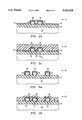
FIG. 1 is a cross-sectional view of a semiconductor wafer on which the present invention has been performed. FIG. 1a shows semiconductor wafer 10 with a substrate 12 which may, for example, contain transistors, diodes, and other semiconductor elements (not shown) as are well known in the art. The substrate 12 may also contain other metal interconnect layers. An aluminum interconnect layer has been deposited over substrate 12. The aluminum interconnect layer has been etched in a predetermined pattern to form etch lines, or aluminum leads 16. Some of the aluminum leads 16 are in close proximity to each other, e.g. less than one micrometer apart. The aluminum leads in ULSI technology (Ultra Large Scale Integration) are typically 0.1 to 0.8 micrometers apart, 0.1 to 0.8 micrometers in width, and have a height of 3 to 4 times the width (giving an aspect ratio of 3:1 to 4:1). It has been found that the tall, thin aluminum leads in ULSI technology are mechanically weak.
FIG. 1b shows the wafer 10 after a strengthened shell 18 has been formed over aluminum leads 16. Strengthened shell 18 is thin and is preferably formed by exposing the aluminum leads 16 to a nitrogen-containing strengthening gas in order to react with the aluminum leads and form a strengthened shell. In the preferred embodiment, rapid thermal annealing is employed using NH3 as the strengthening gas. The resultant strengthened shell 18 can be comprised of, for example, AlN, and is typically 40 to 50 Å thick; approximately twice the thickness of a native oxide, which is generally 20 to 30 Å. Alternately, the aluminum leads 16 may be strengthened by exposure to an oxygen-containing gas, such as N2 O, O2, or O3 to form a strengthened shell 18 of Al2 O3.
As shown in FIG. 1c, dielectric layer 20 may then be deposited over strengthened shell 18 and substrate 12. The dielectric layer 20 of this invention is preferably comprised of a low-dielectric constant material, e.g. a dielectric material having a dielectric constant less than that of SiO2. The dielectric material shown in FIG. 1c is a viscous material that has left air gaps 22 adjacent the strengthening aluminum leads, whereby the air gaps provide a low dielectric medium between the closely-spaced aluminum leads 16.
FIG. 2 is a cross-sectional view of a semiconductor wafer showing an alternate embodiment of the present invention. FIG. 2a shows semiconductor wafer 10 with a substrate 12. Insulating layer 14 has been deposited over the substrate 12 and preferably comprises SiO2. Insulating layer 14 could also comprise PETEOS (plasma-enhanced tetraethosiloxane), BPSG (boron phosphate silicate glass) or other dielectric materials. An aluminum interconnect layer has been deposited over insulating layer 14 and has been etched in a predetermined pattern to form aluminum leads 16.
FIG. 2b shows the wafer 10 after a strengthened shell 18 has been formed over aluminum leads 16 by exposing the wafer to a strengthening gas. The strengthening gas may also react with the exposed portions of insulating layer 14 to form a strengthened insulating layer 19. Like the strengthened shell, the strengthened insulating layer 19 is thin, typically 40 to 50 Å.
Next, dielectric layer 20 is deposited on strengthened shell 18 and strengthened insulating layer 19, as shown in FIG. 2c. The dielectric layer 20 shown in FIG. 2c is a low-dielectric constant material (rather than forming air gaps when applied; however, the material used for the first embodiment could also be used, leaving air gaps between closely-spaced aluminum leads and adjacent to aluminum leads).
In both embodiments shown in FIGS. 1 and 2, subsequent processing steps may then performed as shown in FIG. 3. FIG. 3a shows the aluminum leads 16 with strengthened shell 18, formed as described for FIGS. 1 and 2. FIG. 3b shows the wafer after the dielectric layer 20 has been deposited. The dielectric layer 20 of the wafer 10 is then planarized typically by CMP as shown in FIG. 3c. The strengthened shell 18 strengthens the aluminum leads 16, so that the aluminum leads 16 can withstand the rigorous planarization step, and in addition, the strengthened shell 18 may be used as an etch stop.
Next, a CVD oxide layer 24 may be grown, and can be comprised, for example, of SiO2, as shown in FIG. 3d. Then, a thick oxide layer 26 is deposited (FIG. 3e) and is preferably made of spin-on glass. The wafer may be patterned and etched to remove the thick oxide layer 26, the thin oxide layer 24, and the strengthened shell 18 in predetermined locations. These predetermined locations may create vias, such as via 27 shown in FIG. 3f, that is a hole to the first aluminum layer containing aluminum leads 16. Then a second aluminum layer 28 is deposited which fills via 27 to contact the aluminum leads 16 of the first aluminum layer.
There am many alternatives involved in using the present invention. The present invention can be used on semiconductors using a variety of low-dielectric constant materials. To reduce capacitive coupling for closely-spaced leads, low-dielectric constant materials are being investigated, such as pure polymers (e.g. parylene, teflon, polyimide) or organic spin-on glass (OSOG, e.g. silsequioxane and siloxane glass). Refer to U.S. Pat. No. 4,987,101 issued to Kaanta et al on Jan. 22, 1991 which describes a method for fabricating gas (air) dielectrics; and U.S. Pat. No. 5,103,288 issued to Sakamoto on Apr. 7, 1992 which describes a multilayered wiring structure which decreases capacitance by using a porous dielectric.
The gas used to form the strengthened shell 18 may contain oxygen, nitrogen, or both. Table 2 shows some possible gases that can be used to form the strengthened shell 18 and the strengthened insulating layer 19. Other techniques may be used to form the strengthening shell, which must result in good conformality of the strengthened layers. The steps shown in FIG. 2 could also be applied to the substrate as shown in FIG. 1.
              TABLE 2
______________________________________
Strengthening Strengthened Material
Gas           Layer        Strengthened
______________________________________
NH.sub.3      AlN          Al
N.sub.2 O     Al.sub.2 O.sub.3
                           Al
O.sub.2       Al.sub.2 O.sub.3
                           Al
NH.sub.3      Si.sub.3 N.sub.4
                           SiO.sub.2
O.sub.3       Al.sub.2 O.sub.3
                           Al
______________________________________
FIG. 4 shows another possible embodiment of the invention. The aluminum leads 14 may have a native oxide 30 resident, from exposure to ambient oxygen (FIG. 4a). Exposure to NH3 gas results in the formation of strengthened shell 18 beneath native oxide layer 30, as shown in FIG. 4b. The native oxide 30 may comprise AlO, which is in an unstable chemical state, since there am unpaired molecules (the stable chemical configuration is Al2 O3). Exposure to NH3 may result in some bonding of N to the Al atoms in the native oxide 30, changing the composition of the native oxide 30 to AlON. The result of the invention is the mechanical strengthening of the aluminum leads 16.
The novel method of applying a strengthened shell over aluminum leads to enhance reliability of the leads is beneficial to semiconductors having low-dielectric constant materials. Without first strengthening the aluminum leads with a strengthened shell, the aluminum leads can lack the mechanical strength required to yield a sufficient amount of functional devices per wafer. Low dielectric constant materials have been found to have low structural strength. One advantage of the present invention is to mechanically strengthen the aluminum leads of a semiconductor wafer.
The mechanical properties of the strengthened shell are better than that of unstrengthened aluminum. AlN and Al2 O3 have melting temperatures above 2000° C., which is much higher than the melting of 660° C. for Al. The thermal conductivity of polycrystalline AlN, Al2 O3 and Si3 N4 used to form the strengthening layer is in the order of 30 W/mK at room temperature, which is one order of magnitude higher than SiO2. The thermal conductivity of AlN single crystal is as high as 260 W/mK. The Young's modulus of AlN and Al2 O3 are both approximately 50×106 psi, which is five times the Young's modulus of Al (stress=Young's modulus×strain). Si3 N4 formed by CVD has been used as a passivation layer in microelectronics applications because of its chemical stability, and diffusion barrier properties; and in addition, it has high mechanical strength. Therefore, mechanical benefits of forming the strengthened shell with the above chemistries are evident.
Another advantage of the present invention is that it is an intrinsic operation, rather than extrinsic. The method involves exposing the wafer to a gas, rather than depositing a substance on the wafer. The basic material required is already present on the wafer; it is merely altered. The benefits of an intrinsic process include a cleaner operation than a deposition process, no additional material or layers added to the wafer, and ease of incorporating the process into a cluster tool. A cluster tool provides in situ transfer capability, which eliminates exposing the wafer to oxygen between steps.
While the invention has been described with reference to illustrative embodiments, this description is not intended to be construed in a limiting sense. Various modifications and combinations of the illustrative embodiments, as well as other embodiments of the invention, will be apparent to persons skilled in the art upon reference to the description. It is therefore intended that the appended claims encompass any such modifications or embodiments.
Claims (14)
1. A method for enhancing reliability of aluminum leads of a semiconductor device having a substrate, comprising the steps of:
depositing an aluminum layer on said substrate;
etching said aluminum layer in predetermined pattern to form aluminum leads;
exposing said aluminum leads to a strengthening gas to react with said aluminum leads and form a strengthened shell on said aluminum leads; and
depositing a dielectric layer over said strengthened shell and said substrate, said dielectric layer providing a dielectric constant of less than 3 in a region between at least two of said aluminum leads, whereby the lack of strength of the dielectric material is compensated by stronger aluminum leads.
2. The method of claim 1 wherein said gas contains nitrogen.
3. The method of claim 1 wherein said gas contains oxygen.
4. The method of claim 1 wherein said exposing said aluminum layer step also comprises a rapid thermal anneal.
5. The method of claim 1 wherein said strengthened shell comprises nitrogen and is 10-100 Å thick.
6. The method of claim 1 Wherein said strengthened shell comprises oxygen and is 40-100 Å thick.
7. The method of claim 1 wherein said aluminum leads have an aspect ratio greater than 1.
8. A method for enhancing reliability of aluminum leads of a semiconductor device having a substrate, comprising the steps of:
depositing an insulating layer on said substrate;
depositing an aluminum layer on said insulating layer;
etching said aluminum layer in a predetermined pattern to form aluminum leads, wherein portions of said insulating layer are exposed;
exposing said aluminum leads and said exposed portions of said insulating layer to a strengthening gas in order to react and form a strengthened shell on said aluminum leads and a strengthened insulating layer on said exposed portions of said insulating layer; and
depositing a dielectric layer over said strengthened shell and said strengthened insulating layer, said dielectric layer providing a dielectric constant of less than 3 in a region between at least two of said aluminum leads, whereby the lack of strength of the dielectric material is compensated by stronger aluminum leads.
9. The method of claim 8 wherein said gas contains nitrogen.
10. The method of claim 8 wherein said gas contains oxygen.
11. The method of claim 8 wherein said exposing step also comprises a rapid thermal anneal.
12. The method of claim 8 wherein said strengthened shell and said strengthened insulating layer comprise nitrogen and are 10-100 Å thick.
13. The method of claim 8 wherein said strengthened shell and said strengthened insulating layer comprise oxygen and are 40-100 Å thick.
14. The method of claim 8 wherein said aluminum leads have an aspect ratio greater than 1.
Priority Applications (1)
| Application Number | Priority Date | Filing Date | Title |
|---|---|---|---|
| US08/250,062 US5432128A (en) | 1994-05-27 | 1994-05-27 | Reliability enhancement of aluminum interconnects by reacting aluminum leads with a strengthening gas |
Applications Claiming Priority (1)
| Application Number | Priority Date | Filing Date | Title |
|---|---|---|---|
| US08/250,062 US5432128A (en) | 1994-05-27 | 1994-05-27 | Reliability enhancement of aluminum interconnects by reacting aluminum leads with a strengthening gas |
Publications (1)
| Publication Number | Publication Date |
|---|---|
| US5432128A true US5432128A (en) | 1995-07-11 |
Family
ID=22946164
Family Applications (1)
| Application Number | Title | Priority Date | Filing Date |
|---|---|---|---|
| US08/250,062 Expired - Lifetime US5432128A (en) | 1994-05-27 | 1994-05-27 | Reliability enhancement of aluminum interconnects by reacting aluminum leads with a strengthening gas |
Country Status (1)
| Country | Link |
|---|---|
| US (1) | US5432128A (en) |
Cited By (19)
| Publication number | Priority date | Publication date | Assignee | Title |
|---|---|---|---|---|
| US5498571A (en) * | 1993-04-13 | 1996-03-12 | Kabushiki Kaisha Toshiba | Method of manufacturing a semiconductor device having reliable multi-layered wiring |
| US5665644A (en) * | 1995-11-03 | 1997-09-09 | Micron Technology, Inc. | Semiconductor processing method of forming electrically conductive interconnect lines and integrated circuitry |
| US5691573A (en) * | 1995-06-07 | 1997-11-25 | Advanced Micro Devices, Inc. | Composite insulation with a dielectric constant of less than 3 in a narrow space separating conductive lines |
| US5744865A (en) * | 1996-10-22 | 1998-04-28 | Texas Instruments Incorporated | Highly thermally conductive interconnect structure for intergrated circuits |
| US5776832A (en) * | 1996-07-17 | 1998-07-07 | Taiwan Semiconductor Manufacturing Company Ltd. | Anti-corrosion etch process for etching metal interconnections extending over and within contact openings |
| US5789819A (en) * | 1994-05-20 | 1998-08-04 | Texas Instruments Incorporated | Low dielectric constant material for electronics applications |
| US5858871A (en) * | 1994-05-27 | 1999-01-12 | Texas Instruments Incorporated | Porous insulator for line-to-line capacitance reduction |
| US5877557A (en) * | 1996-04-01 | 1999-03-02 | Raytheon Company | Low temperature aluminum nitride |
| US5976979A (en) * | 1997-06-10 | 1999-11-02 | Industrial Technology Research Institute | Sequential oxygen plasma treatment and chemical mechanical polish (CMP) planarizing method for forming planarized low dielectric constant dielectric layer |
| US6091150A (en) * | 1996-09-03 | 2000-07-18 | Micron Technology, Inc. | Integrated circuitry comprising electrically insulative material over interconnect line tops, sidewalls and bottoms |
| US6153937A (en) * | 1996-07-16 | 2000-11-28 | Kabushiki Kaisha Toshiba | Semiconductor device and method of the same |
| US6218295B1 (en) * | 1996-05-08 | 2001-04-17 | Micron Technology, Inc. | Semiconductor structure with a titanium aluminum nitride layer and method for fabricating the same |
| US6297538B1 (en) | 1998-03-23 | 2001-10-02 | The University Of Delaware | Metal-insulator-semiconductor field effect transistor having an oxidized aluminum nitride gate insulator formed on a gallium nitride or silicon substrate |
| US6362527B1 (en) * | 1996-11-21 | 2002-03-26 | Advanced Micro Devices, Inc. | Borderless vias on bottom metal |
| US6566757B1 (en) * | 1998-11-30 | 2003-05-20 | Intel Corporation | Stabilization of low dielectric constant film with in situ capping layer |
| US6577007B1 (en) * | 1996-02-01 | 2003-06-10 | Advanced Micro Devices, Inc. | Manufacturing process for borderless vias with respect to underlying metal |
| US6777320B1 (en) * | 1998-11-13 | 2004-08-17 | Intel Corporation | In-plane on-chip decoupling capacitors and method for making same |
| US20050106860A1 (en) * | 2003-11-17 | 2005-05-19 | Ming-Hsiu Lee | [method of fabricating a contact] |
| US6933230B2 (en) * | 1998-12-31 | 2005-08-23 | Intel Corporation | Method for making interconnects and diffusion barriers in integrated circuits |
Citations (4)
| Publication number | Priority date | Publication date | Assignee | Title |
|---|---|---|---|---|
| US3887994A (en) * | 1973-06-29 | 1975-06-10 | Ibm | Method of manufacturing a semiconductor device |
| US4920077A (en) * | 1987-10-09 | 1990-04-24 | Sgs-Thomson Microelectronics S.R.L. | Method of manufacturing monolythic integrated circuits |
| US4987101A (en) * | 1988-12-16 | 1991-01-22 | International Business Machines Corporation | Method for providing improved insulation in VLSI and ULSI circuits |
| US5103288A (en) * | 1988-03-15 | 1992-04-07 | Nec Corporation | Semiconductor device having multilayered wiring structure with a small parasitic capacitance |
-
1994
- 1994-05-27 US US08/250,062 patent/US5432128A/en not_active Expired - Lifetime
Patent Citations (4)
| Publication number | Priority date | Publication date | Assignee | Title |
|---|---|---|---|---|
| US3887994A (en) * | 1973-06-29 | 1975-06-10 | Ibm | Method of manufacturing a semiconductor device |
| US4920077A (en) * | 1987-10-09 | 1990-04-24 | Sgs-Thomson Microelectronics S.R.L. | Method of manufacturing monolythic integrated circuits |
| US5103288A (en) * | 1988-03-15 | 1992-04-07 | Nec Corporation | Semiconductor device having multilayered wiring structure with a small parasitic capacitance |
| US4987101A (en) * | 1988-12-16 | 1991-01-22 | International Business Machines Corporation | Method for providing improved insulation in VLSI and ULSI circuits |
Non-Patent Citations (14)
| Title |
|---|
| "Standard Method of Test For Young's Modulus At Room Temperatures", ASTM E111-61, op-cit., pp. 1-6. |
| James F. Shackelford and William Alexander, "The CRC Materials Science And Engineering Handbook", p. 336 and 338, (CRC Press, 1992). |
| James F. Shackelford and William Alexander, The CRC Materials Science And Engineering Handbook , p. 336 and 338, (CRC Press, 1992). * |
| Jochen Fricke and Andreas Emmerling, "Aerogels", May 28, 1992, J. Am. Seram. Soc. 75(8)pp. 2027-2036. |
| Jochen Fricke and Andreas Emmerling, Aerogels , May 28, 1992, J. Am. Seram. Soc. 75(8)pp. 2027 2036. * |
| Standard Method of Test For Young s Modulus At Room Temperatures , ASTM E111 61, op cit., pp. 1 6. * |
| T. Osaka, T. Asada, E. Nakajima, and I. Koiwa, "Chemical Etching Properties of Highly Thermal Conductive AIN Ceramic For Electroless Ni-P Metallization", J. Electrochem. Soc.: Solid State Science an Technol., 135, 2578-2581 (1988). |
| T. Osaka, T. Asada, E. Nakajima, and I. Koiwa, Chemical Etching Properties of Highly Thermal Conductive AIN Ceramic For Electroless Ni P Metallization , J. Electrochem. Soc.: Solid State Science an Technol., 135, 2578 2581 (1988). * |
| W. D. Kingery, H. K. Bowen, and D. R. Uhlmann, "Introduction to Ceramics", 2nd Ed., p. 777 (John Wiley & Sons, New York, 1976). |
| W. D. Kingery, H. K. Bowen, and D. R. Uhlmann, Introduction to Ceramics , 2nd Ed., p. 777 (John Wiley & Sons, New York, 1976). * |
| Wolf & Tauber "Silicon Process for the VLSI Era" vol. 1 Lattice Press pp. 57-58. |
| Wolf & Tauber Silicon Process for the VLSI Era vol. 1 Lattice Press pp. 57 58. * |
| Yasuhiro Kurokawa, Hiroyuki Hamaguchi, Yuzo Shimada, Kazuaki Utsumi and Hideo Takamizawa, "Highly Thermal Conductive Aluminum Nitride Substrates", ISHM '87 Proceedings, pp. 654-661. |
| Yasuhiro Kurokawa, Hiroyuki Hamaguchi, Yuzo Shimada, Kazuaki Utsumi and Hideo Takamizawa, Highly Thermal Conductive Aluminum Nitride Substrates , ISHM 87 Proceedings, pp. 654 661. * |
Cited By (30)
| Publication number | Priority date | Publication date | Assignee | Title |
|---|---|---|---|---|
| US5498571A (en) * | 1993-04-13 | 1996-03-12 | Kabushiki Kaisha Toshiba | Method of manufacturing a semiconductor device having reliable multi-layered wiring |
| US5759912A (en) * | 1993-04-13 | 1998-06-02 | Kabushiki Kaisha Toshiba | Method of manufacturing a semiconductor device having multi-layered wiring without hillocks at the insulating layers |
| US5789819A (en) * | 1994-05-20 | 1998-08-04 | Texas Instruments Incorporated | Low dielectric constant material for electronics applications |
| US5858871A (en) * | 1994-05-27 | 1999-01-12 | Texas Instruments Incorporated | Porous insulator for line-to-line capacitance reduction |
| US5691573A (en) * | 1995-06-07 | 1997-11-25 | Advanced Micro Devices, Inc. | Composite insulation with a dielectric constant of less than 3 in a narrow space separating conductive lines |
| US6048802A (en) * | 1995-06-07 | 2000-04-11 | Advanced Micro Devices, Inc. | Selective nonconformal deposition for forming low dielectric insulation between certain conductive lines |
| US5910684A (en) * | 1995-11-03 | 1999-06-08 | Micron Technology, Inc. | Integrated circuitry |
| US6432813B1 (en) * | 1995-11-03 | 2002-08-13 | Micron Technology, Inc. | Semiconductor processing method of forming insulative material over conductive lines |
| US6066553A (en) * | 1995-11-03 | 2000-05-23 | Micron Technology, Inc. | Semiconductor processing method of forming electrically conductive interconnect lines and integrated circuitry |
| US5665644A (en) * | 1995-11-03 | 1997-09-09 | Micron Technology, Inc. | Semiconductor processing method of forming electrically conductive interconnect lines and integrated circuitry |
| US6577007B1 (en) * | 1996-02-01 | 2003-06-10 | Advanced Micro Devices, Inc. | Manufacturing process for borderless vias with respect to underlying metal |
| US5877557A (en) * | 1996-04-01 | 1999-03-02 | Raytheon Company | Low temperature aluminum nitride |
| US6552431B2 (en) | 1996-05-08 | 2003-04-22 | Micron Technology, Inc. | Semiconductor structure with a titanium aluminum nitride layer and method for fabricating same |
| US6218295B1 (en) * | 1996-05-08 | 2001-04-17 | Micron Technology, Inc. | Semiconductor structure with a titanium aluminum nitride layer and method for fabricating the same |
| US6239492B1 (en) | 1996-05-08 | 2001-05-29 | Micron Technology, Inc. | Semiconductor structure with a titanium aluminum nitride layer and method for fabricating same |
| US6153937A (en) * | 1996-07-16 | 2000-11-28 | Kabushiki Kaisha Toshiba | Semiconductor device and method of the same |
| US5776832A (en) * | 1996-07-17 | 1998-07-07 | Taiwan Semiconductor Manufacturing Company Ltd. | Anti-corrosion etch process for etching metal interconnections extending over and within contact openings |
| US6091150A (en) * | 1996-09-03 | 2000-07-18 | Micron Technology, Inc. | Integrated circuitry comprising electrically insulative material over interconnect line tops, sidewalls and bottoms |
| US5744865A (en) * | 1996-10-22 | 1998-04-28 | Texas Instruments Incorporated | Highly thermally conductive interconnect structure for intergrated circuits |
| US6362527B1 (en) * | 1996-11-21 | 2002-03-26 | Advanced Micro Devices, Inc. | Borderless vias on bottom metal |
| US5976979A (en) * | 1997-06-10 | 1999-11-02 | Industrial Technology Research Institute | Sequential oxygen plasma treatment and chemical mechanical polish (CMP) planarizing method for forming planarized low dielectric constant dielectric layer |
| US6297538B1 (en) | 1998-03-23 | 2001-10-02 | The University Of Delaware | Metal-insulator-semiconductor field effect transistor having an oxidized aluminum nitride gate insulator formed on a gallium nitride or silicon substrate |
| US6593194B2 (en) | 1998-03-23 | 2003-07-15 | University Of Delaware | Metal-insulator-semiconductor field effect transistor having an oxidized aluminum nitride gate insulator formed on a gallium nitride or silicon substrate, and method of making the same |
| US6777320B1 (en) * | 1998-11-13 | 2004-08-17 | Intel Corporation | In-plane on-chip decoupling capacitors and method for making same |
| US20040245606A1 (en) * | 1998-11-13 | 2004-12-09 | Chien Chiang | In-plane on-chip decoupling capacitors and method for making same |
| US6949831B2 (en) | 1998-11-13 | 2005-09-27 | Intel Corporation | In-plane on-chip decoupling capacitors and method for making same |
| US6566757B1 (en) * | 1998-11-30 | 2003-05-20 | Intel Corporation | Stabilization of low dielectric constant film with in situ capping layer |
| US6933230B2 (en) * | 1998-12-31 | 2005-08-23 | Intel Corporation | Method for making interconnects and diffusion barriers in integrated circuits |
| US20050106860A1 (en) * | 2003-11-17 | 2005-05-19 | Ming-Hsiu Lee | [method of fabricating a contact] |
| US6964879B2 (en) * | 2003-11-17 | 2005-11-15 | Macronix International Co., Ltd. | Method of fabricating a contact |
Similar Documents
| Publication | Publication Date | Title |
|---|---|---|
| US5432128A (en) | Reliability enhancement of aluminum interconnects by reacting aluminum leads with a strengthening gas | |
| US5519250A (en) | Reliability of metal leads in high speed LSI semiconductors using both dummy leads and thermoconductive layers | |
| US5675187A (en) | Reliability of metal leads in high speed LSI semiconductors using dummy vias | |
| US5461003A (en) | Multilevel interconnect structure with air gaps formed between metal leads | |
| US5751056A (en) | Reliable metal leads in high speed LSI semiconductors using dummy leads | |
| US7119441B2 (en) | Semiconductor interconnect structure | |
| US7091611B2 (en) | Multilevel copper interconnects with low-k dielectrics and air gaps | |
| US6057226A (en) | Air gap based low dielectric constant interconnect structure and method of making same | |
| US5565384A (en) | Self-aligned via using low permittivity dielectric | |
| US5786624A (en) | Dual masking for selective gap fill of submicron interconnects | |
| US5510293A (en) | Method of making reliable metal leads in high speed LSI semiconductors using thermoconductive layers | |
| US6445072B1 (en) | Deliberate void in innerlayer dielectric gapfill to reduce dielectric constant | |
| US5814558A (en) | Interconnect capacitance between metal leads | |
| JP3696055B2 (en) | Manufacturing method of semiconductor device | |
| US8957519B2 (en) | Structure and metallization process for advanced technology nodes | |
| US20060207965A1 (en) | Method to form both high and low-k materials over the same dielectric region, and their application in mixed mode circuits | |
| US6166411A (en) | Heat removal from SOI devices by using metal substrates | |
| US7410896B2 (en) | Semiconductor device having low-k dielectric film in pad region and method for manufacture thereof | |
| US6376359B1 (en) | Method of manufacturing metallic interconnect | |
| JPH0794441A (en) | Semiconductor device and its manufacture | |
| GB2371146A (en) | Dual damascene interconnect between conducting layers of integrated circuit | |
| KR19990065101A (en) | Method of forming interlayer insulating film of semiconductor device | |
| JPH0621242A (en) | Semiconductor device and manufacture thereof | |
| JPH08274168A (en) | Manufacture of semiconductor device |
Legal Events
| Date | Code | Title | Description |
|---|---|---|---|
| AS | Assignment |
Owner name: TEXAS INSTRUMENTS INCORPORATED, TEXAS Free format text: ASSIGNMENT OF ASSIGNORS INTEREST;ASSIGNOR:TSU, ROBERT;REEL/FRAME:007021/0022 Effective date: 19940526 |
|
| STCF | Information on status: patent grant |
Free format text: PATENTED CASE |
|
| FPAY | Fee payment |
Year of fee payment: 4 |
|
| FPAY | Fee payment |
Year of fee payment: 8 |
|
| FPAY | Fee payment |
Year of fee payment: 12 |