US5430632A - Self-oscillating DC to DC converter - Google Patents
Self-oscillating DC to DC converter Download PDFInfo
- Publication number
- US5430632A US5430632A US08/255,991 US25599194A US5430632A US 5430632 A US5430632 A US 5430632A US 25599194 A US25599194 A US 25599194A US 5430632 A US5430632 A US 5430632A
- Authority
- US
- United States
- Prior art keywords
- windings
- electrode
- pair
- transistor means
- source
- Prior art date
- Legal status (The legal status is an assumption and is not a legal conclusion. Google has not performed a legal analysis and makes no representation as to the accuracy of the status listed.)
- Expired - Lifetime
Links
Images


Classifications
-
- H—ELECTRICITY
- H02—GENERATION; CONVERSION OR DISTRIBUTION OF ELECTRIC POWER
- H02M—APPARATUS FOR CONVERSION BETWEEN AC AND AC, BETWEEN AC AND DC, OR BETWEEN DC AND DC, AND FOR USE WITH MAINS OR SIMILAR POWER SUPPLY SYSTEMS; CONVERSION OF DC OR AC INPUT POWER INTO SURGE OUTPUT POWER; CONTROL OR REGULATION THEREOF
- H02M3/00—Conversion of dc power input into dc power output
- H02M3/22—Conversion of dc power input into dc power output with intermediate conversion into ac
- H02M3/24—Conversion of dc power input into dc power output with intermediate conversion into ac by static converters
- H02M3/28—Conversion of dc power input into dc power output with intermediate conversion into ac by static converters using discharge tubes with control electrode or semiconductor devices with control electrode to produce the intermediate ac
- H02M3/325—Conversion of dc power input into dc power output with intermediate conversion into ac by static converters using discharge tubes with control electrode or semiconductor devices with control electrode to produce the intermediate ac using devices of a triode or a transistor type requiring continuous application of a control signal
- H02M3/335—Conversion of dc power input into dc power output with intermediate conversion into ac by static converters using discharge tubes with control electrode or semiconductor devices with control electrode to produce the intermediate ac using devices of a triode or a transistor type requiring continuous application of a control signal using semiconductor devices only
- H02M3/338—Conversion of dc power input into dc power output with intermediate conversion into ac by static converters using discharge tubes with control electrode or semiconductor devices with control electrode to produce the intermediate ac using devices of a triode or a transistor type requiring continuous application of a control signal using semiconductor devices only in a self-oscillating arrangement
- H02M3/3382—Conversion of dc power input into dc power output with intermediate conversion into ac by static converters using discharge tubes with control electrode or semiconductor devices with control electrode to produce the intermediate ac using devices of a triode or a transistor type requiring continuous application of a control signal using semiconductor devices only in a self-oscillating arrangement in a push-pull circuit arrangement
-
- Y—GENERAL TAGGING OF NEW TECHNOLOGICAL DEVELOPMENTS; GENERAL TAGGING OF CROSS-SECTIONAL TECHNOLOGIES SPANNING OVER SEVERAL SECTIONS OF THE IPC; TECHNICAL SUBJECTS COVERED BY FORMER USPC CROSS-REFERENCE ART COLLECTIONS [XRACs] AND DIGESTS
- Y02—TECHNOLOGIES OR APPLICATIONS FOR MITIGATION OR ADAPTATION AGAINST CLIMATE CHANGE
- Y02B—CLIMATE CHANGE MITIGATION TECHNOLOGIES RELATED TO BUILDINGS, e.g. HOUSING, HOUSE APPLIANCES OR RELATED END-USER APPLICATIONS
- Y02B70/00—Technologies for an efficient end-user side electric power management and consumption
- Y02B70/10—Technologies improving the efficiency by using switched-mode power supplies [SMPS], i.e. efficient power electronics conversion e.g. power factor correction or reduction of losses in power supplies or efficient standby modes
Definitions
- This invention relates in general to DC to DC converters, and more particularly to DC to DC converters which employ a half-bridge configuration and which operate in a self-oscillating mode.
- Direct current to direct current (DC to DC) converters which employ a half-bridge configuration and which operate in a self-oscillating mode, are commonly realized by converter topologies which are referred to in the art as resonant pole converters. These converters have zero voltage switching and are classified into three categories: linear resonant pole, non-linear resonant pole, and double non-linear resonant pole.
- Resonant pole converters are characterized by simple circuit designs which integrate some of the circuit parasitics into the required functionality. However, operation of such converters at higher frequencies becomes extremely difficult to achieve without sacrificing efficiency and without producing high levels of electromagnetic interference.
- the frequency of operation for prior art converters is limited to approximately 200 kHz.
- the double non-linear resonant pole converter has been developed which has lowered switching losses, reduced parasitic oscillations, etc., as disclosed in the "Study of a Generic Topology for a Double Non-Linear Resonant Pole Converter" by J. R. DeV Amsterdam. J. D. Van Wyk, J. A. Ferreira, IEEE Power Electronics Specialist Conference, 1992, pages 633-638.
- a non-linear capacitor is utilized as a regenerative snubber in the aforesaid topology.
- the inventor has recognized the desirability of a conversion topology which operates at a very high frequency (ie. into the MHz range), which integrates the major device and component parasitics thereby simplifying the circuit design, and which provides a simple means of regulation of the output voltage regardless of line and load variations.
- the existing topologies do not offer solutions to these problems.
- the present invention provides a new topology for DC to DC conversion in which a very high degree of integration of all major parasitics, both inductive and capacitive, is achieved.
- a direct current to direct current (DC to DC) self-oscillating converter which uses a pair of switching transistors connected in a half bridge configuration to respective drive signal windings of an isolated gate drive transformer in such a way that all intrinsic capacitances of the transistors are fully incorporated into the functionality of the converter.
- the transistors are connected, in turn, to the primary winding of an output isolation transformer.
- a start-up circuit is provided to initiate the oscillation of the half bridge.
- the gate-to-source intrinsic capacitance of the transistors serves to provide the necessary tank capacitance, while the drain-to-source intrinsic capacitance of the transistors, in combination with the inductance of the load, functions as a regenerative snubber, and the intrinsic gate-to-drain capacitance of the transistors serves to provide the necessary feedback for the converter.
- variable inductance (L M ) of the isolated gate drive transformer serves as the frequency controlling inductance of a frequency determining circuit for the converter. Regulation of the converter is achieved by passing a small direct current through the control windings of the isolated gate drive transformer which causes a change in its inductance and in turn, the frequency of oscillation.
- a zener diode can be used as a simple means to implement the control function. Accordingly, the circuit of the present invention can operate without any external capacitor, greatly reducing parasitic oscillatory tendencies, and at the same time providing a convenient means for regulation.
- the magnetic feedback eliminates the need for use of an optocoupler.
- the change in frequency of the converter is utilized to vary the output power via resonant means where an equivalent resonant tank inductor is provided by the leakage inductance (L L ) of the output isolation transformer and an equivalent resonant capacitor is provided by the capacitance presented by the output rectification circuitry.
- L L leakage inductance
- the ability to utilize a high leakage transformer for the output isolation transformer facilitates and simplifies adherence to legislated safety standards.
- This increased integration of parasitic elements of the converter provides a significant increase in the power density over prior art resonant converters, while keeping parasitic oscillations to a minimum, and thus lowering EMI.
- Regulated multiple outputs can be obtained by tight coupling of the output windings to the secondary winding that carries the highest power.
- the number of cross-regulated outputs is limited only by the construction of the transformer.
- the output isolation transformer provides effective decoupling of the common mode noise, and is characterized by reduced primary to secondary capacitance.
- the DC to DC self-oscillating converter of the present invention can be used in a full bridge configuration by the addition of two windings to the isolated gate drive transformer, thereby extending the power handling limitations of the circuit to the kW range.
- topology of the present invention is AC to DC conversion, wherein a simple diode bridge may be added to convert the AC current to the required DC for input to the DC to DC converter of the preferred embodiment.
- This arrangement results in power factors approaching unity, thereby facilitating use of the converter as a pre-regulator with power factor correction.
- topology of the present invention is generation of high power, high frequency sinusoidal waves.
- the RF energy generated in this manner can be used to drive an antenna for radio-transmission or for use with an ultrasonic transducer for industrial or medical purposes.
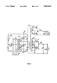
- FIG. 1 is a detailed circuit diagram of a MOSFET half-bridge, self oscillating, cross regulated resonant converter in accordance with the preferred embodiment
- FIG. 2 is an equivalent circuit of the preferred embodiment illustrated in FIG. 1;
- FIGS. 3a, 3b and 3c show the waveforms of the drain-to-source voltage, gate-to-source voltage and current flowing through the drain-to-gate intrinsic capacitances, respectively, of a MOSFET switch of the circuit shown in FIGS. 1 and 2;
- FIG. 4 is a detailed circuit diagram of an alternative embodiment of the invention wherein the converter is utilized for AC to DC conversion;
- FIG. 5 is a detailed schematic diagram of a full-bridge, self oscillating, resonant converter in accordance with a further alternative embodiment of the invention.
- FIG. 1 is a schematic diagram of a self-oscillating, cross-regulated resonant converter in accordance with the preferred embodiment comprising two MOSFET transistors 10 and 11 connected to an isolated gate drive transformer 42 consisting of control windings 5 and 6 and drive signal windings 7 and 8.
- the gate of MOSFET transistor 10 is connected to the dotted end of drive signal winding 7 and the drain is connected to the positive DC input lead 9.
- the gate of MOSFET transistor 11 is connected to the undotted end of drive signal winding 8 and the source is connected to the negative DC input lead 12 and also to the dotted end of drive signal winding 8.
- the undotted end of gate drive inductor 7 is connected to the midpoint of the source-to-drain connection between MOSFET transistors 10 and 11.
- control winding 5 is connected to the dotted end of control winding 6.
- the undotted end of control winding 5 and the undotted end of control winding 6 of the isolated gate drive transformer 42 are connected to a controller 24.
- a decoupling capacitor 13 is fed by the positive DC input lead 9 and in turn is connected to decoupling capacitor 14 which is fed by the negative DC input lead 12.
- MOSFET transistors for rectification 20 and 21 are connected to secondary windings 17 and 18, and also to the rectification control windings 16 and 19 of the output isolation transformer.
- the gate of MOSFET transistor 20 is connected to the dotted end rectification of control winding 16 and the source is connected to the undotted end of rectification control winding 16 which, in turn, is connected to the dotted end of secondary winding 17.
- the undotted end of winding 17 is connected to the dotted end of secondary winding 18 which, in turn, is connected to the undotted end of rectification control winding 19 and also to the source of MOSFET transistor 21.
- the gate of MOSFET transistor 21 is connected to the dotted end rectification of control winding 19.
- the start-up circuit of the converter comprises a start-up resistor 1 connected to a start-up capacitor 2 and also to a voltage sensitive trigger diode 3 which is connected to the gate of MOSFET transistor 11.
- One end of an output filter inductor 22 is connected to the midpoint of the drain-to-drain connection between MOSFETs 20 and 21, and the other end is connected to an output filter capacitor 23 and the positive end of load 28.
- the other end of filter capacitor 23 is connected to the junction point of secondary windings 17 and 18 and also to the negative end of load 28.
- An auxiliary output of the converter comprises second output windings 29 and 30 where the dotted end of output winding 29 is connected to a first output rectifier 31.
- the undotted end of output winding 29 is connected to the dotted end of output winding 30.
- the undotted end of winding 30 is connected to a second output rectifier 32.
- a second output filter inductor 33 is connected to the midpoint of the connection between rectifiers 31 and 32, and also to a second output filter capacitor 34 which is connected in parallel to a load 35.
- the other end of output filter capacitor 34 is connected to the junction point of output windings 29 and 30.
- FIG. 2 is a schematic diagram of an equivalent circuit of the preferred embodiment where two ideal MOSFETs 50 and 51 are connected to drive signal windings 7 and 8, respectively, which, for the purpose of the equivalent circuit of FIG. 2, form an equivalent gate tank inductance.
- the gate of MOSFET 50 is connected to the dotted end of drive signal winding 7 and the source is connected to the undotted end of drive signal winding 7.
- An equivalent gate-to-source capacitance 47 is connected in parallel to drive signal winding 7 and in series with an equivalent gate-to-drain capacitance 46 which is, in turn, connected to the drain of MOSFET 50.
- An equivalent drain-to-source capacitance 52 is connected in parallel to MOSFET 50.
- MOSFET 51 is connected to the undotted end of drive signal winding 8 and the source is connected to the dotted end of drive signal winding 8.
- An equivalent gate-to-source capacitance 49 is connected in parallel to drive signal winding 8 and in series with an equivalent gate-to-drain capacitance 48 which is in turn connected to the drain of MOSFET 51.
- An equivalent drain-to-source capacitance 53 is connected in parallel to MOSFET 51.
- One end of an equivalent resonant tank inductor 54 is connected to the midpoint of the source-to-drain connection between MOSFETs 50 and 51 while the other end is connected to an equivalent resonant capacitor 55 which is connected in parallel to a load resistance 56.
- the equivalent resonant capacitor 55 is derived from the intrinsic gate-to-source capacitance of the rectification MOSFETs 20 and 21.
- the parallel combination of resistor 56 and capacitor 55 is connected to the midpoint of the negative to positive connection of voltage sources 57 and 58.
- the positive terminal of voltage source 57 is connected to the drain of MOSFET 50 and the negative terminal of voltage source 58 is connected to the source of MOSFET 51.
- MOSFET transistors 10 and 11 are both in an "off" state.
- start-up capacitor 2 begins to charge through resistor 1 until the threshold voltage of voltage sensitive trigger diode 3 is reached.
- the stored energy in capacitor 2 is dumped into the gate resonant tank consisting of the drive signal windings 7 and 8, and gate-to-source capacitances 47 and 49 of the MOSFET transistors as shown in FIG. 2. This results in a rising gate drive signal supported by the capacitive feedback until, in any given cycle, an equilibrium is established between the feedback energy and the energy lost in the resonant tank.
- a sinusoidal gate drive signal appears across the gate to source electrodes of MOSFET 11 while drive transformer 42 inverts the same signal across the gate to source electrodes of MOSFET 10.
- the gate voltage of MOSFET transistor 11 falls below the "on" level (V G in FIG. 3b )
- the current stored in the equivalent resonant tank inductor 54 begins to charge the drain-to-source equivalent capacitances 53 and 52 of transistors 11 and 10, resulting in the trapezoidal voltage waveform shown in FIG. 3a.
- the rising and falling edges of the waveform in FIG. 3a represents the aforementioned charging process.
- a current pulse (as shown in FIG.
- This equation expresses the fact that the absorbed energy (E abs ) per cycle in the resonant tank has to be equal to the energy packages delivered to the resonant tank in each cycle in order to achieve constant amplitude.
- the incremental voltage change can be expressed as: ##EQU2##
- Equation (2) Substituting Equations (1) and (3) into Equation (2) results in: ##EQU3##
- the control of the converter's frequency is achieved by varying the inductance of the drive transformer 42.
- One straightforward manner of constructing a drive transformer with variable inductance is to use two cores, each having a control winding installed on it, wherein the control windings are connected in series (ie. windings 5 and 6 in FIGS. 1 and 2).
- the drive signal windings 7 and 8 which perform the inverting of the gate drive signal are installed so as to share the two magnetic cores since it is desirable to minimize the leakage inductance in order to avoid parasitic oscillations.
- the current flowing through the control windings 5 and 6 reduces the inductance of the drive transformer which in turn increases the resonant frequency (F r ) of the gate tank circuit: ##EQU4## where
- FIG. 4 shows a schematic diagram of an alternative to the preferred embodiment which is in the form of an AC to DC regulated converter with high power factor.
- Rectifiers 36, 37, 38, and 39 are utilized to convert an AC current at terminals 40 and 4, to a direct current which powers the circuit at the equivalent points to the positive and negative DC inputs 9 and 12, respectively, shown in FIG. 1.
- Peak rectifier 25 and peak holding capacitor 26 form a peak detector circuit.
- the peak ripple voltage is sensed by zener diode 27, thereby providing a simple means to achieve control of the frequency by the control current flowing through zener diode 27 and control windings 5 and 6.
- FIG. 5 is a schematic diagram of a further alternative embodiment for achieving higher power levels than are attainable by the embodiments discussed above.
- a full-bridge configuration is provided by the addition of MOSFET transistors 44 and 45 and additional drive signal windings 59 and 60.
- the gate of MOSFET transistor 44 is connected to the undotted end of drive signal winding 59, and the drain is connected to the junction of start-up resistor 1 and the positive DC input lead 9.
- the gate of MOSFET transistor 45 is connected to the dotted end of drive signal winding 60, and the source is connected to the undotted end of drive signal winding 60.
- the midpoint of the drain-to-source connection between MOSFET transistors 44 and 45 is connected to the primary winding 15 of the output isolation transformer 43.
- a self oscillating power converter comprising a minimum number of components which perform multiple functions.
- the isolation transformer not only provides isolation while converting the output voltage to a desired value, it also provides integration of the resonant inductor and gives multiple output capabilities.
- Thermal protection can be achieved by using a magnetic core with a low curie temperature for construction of the isolated gate drive transformer.
Abstract
Description
E.sub.abs =1/2C.sub.m (ΔV).sup.2 (2)
C.sub.r =C.sub.49 +C.sub.47 (6)
Claims (14)
Priority Applications (1)
| Application Number | Priority Date | Filing Date | Title |
|---|---|---|---|
| PCT/CA1995/000195 WO1995033300A1 (en) | 1994-05-26 | 1995-04-10 | Self-oscillating dc to dc converter |
Applications Claiming Priority (2)
| Application Number | Priority Date | Filing Date | Title |
|---|---|---|---|
| CA002124370A CA2124370C (en) | 1994-05-26 | 1994-05-26 | Self oscillating dc to dc converter |
| CA2124370 | 1994-05-26 |
Publications (1)
| Publication Number | Publication Date |
|---|---|
| US5430632A true US5430632A (en) | 1995-07-04 |
Family
ID=4153675
Family Applications (1)
| Application Number | Title | Priority Date | Filing Date |
|---|---|---|---|
| US08/255,991 Expired - Lifetime US5430632A (en) | 1994-05-26 | 1994-06-08 | Self-oscillating DC to DC converter |
Country Status (6)
| Country | Link |
|---|---|
| US (1) | US5430632A (en) |
| EP (1) | EP0761036B1 (en) |
| AU (1) | AU2210295A (en) |
| CA (1) | CA2124370C (en) |
| DE (1) | DE69504501T2 (en) |
| WO (1) | WO1995033300A1 (en) |
Cited By (34)
| Publication number | Priority date | Publication date | Assignee | Title |
|---|---|---|---|---|
| US5539630A (en) * | 1993-11-15 | 1996-07-23 | California Institute Of Technology | Soft-switching converter DC-to-DC isolated with voltage bidirectional switches on the secondary side of an isolation transformer |
| US5541827A (en) * | 1995-05-17 | 1996-07-30 | Doble Engineering Company | Reducing switching losses in a phase-modulated switch-mode amplifier |
| US5880939A (en) * | 1996-09-06 | 1999-03-09 | Sinfor | Stabilized power supply circuit including hyperresonant chopping and synchronous rectification |
| US6108219A (en) * | 1999-01-06 | 2000-08-22 | Indigo Manufacturing Inc. | DC power converter circuit |
| US6259615B1 (en) | 1999-07-22 | 2001-07-10 | O2 Micro International Limited | High-efficiency adaptive DC/AC converter |
| US6466467B2 (en) * | 2000-12-22 | 2002-10-15 | Patricio Lagos Lehuede | Inverter or converter by current injection, provided with a circuit whose generating frequency for the alternating voltage is adjusted by the load's resonant frequency, cycle to cycle, without lags |
| US20020180403A1 (en) * | 2001-05-24 | 2002-12-05 | Brown Fred A. | Efficient stator |
| US6501234B2 (en) | 2001-01-09 | 2002-12-31 | 02 Micro International Limited | Sequential burst mode activation circuit |
| US6531831B2 (en) | 2000-05-12 | 2003-03-11 | O2Micro International Limited | Integrated circuit for lamp heating and dimming control |
| US6560127B2 (en) * | 2000-05-04 | 2003-05-06 | Texas Instruments Incorporated | Power conversion circuit having improved zero voltage switching |
| US6570344B2 (en) | 2001-05-07 | 2003-05-27 | O2Micro International Limited | Lamp grounding and leakage current detection system |
| US20030123263A1 (en) * | 2001-12-27 | 2003-07-03 | Caterpillar Inc. | Controller area network using transformers |
| US20030227452A1 (en) * | 2002-06-07 | 2003-12-11 | Alexandru Hartular | Adaptive LCD power supply circuit |
| US6710554B2 (en) * | 2002-02-27 | 2004-03-23 | Wireless Methods Ltd. | Dimmer arrangement for gas discharge lamp with inductive ballast |
| US6756769B2 (en) | 2002-06-20 | 2004-06-29 | O2Micro International Limited | Enabling circuit for avoiding negative voltage transients |
| WO2004062075A2 (en) | 2002-12-31 | 2004-07-22 | Apogee Technology, Inc. | Adaptive resonant switching power system |
| US20040178781A1 (en) * | 2003-01-22 | 2004-09-16 | Yung-Lin Lin | Controller and driving method for power circuits, electrical circuit for supplying energy and display device having the electrical circuit |
| US20040189095A1 (en) * | 2003-03-25 | 2004-09-30 | Yung-Lin Lin | Integrated power supply for an LCD panel |
| US6804129B2 (en) | 1999-07-22 | 2004-10-12 | 02 Micro International Limited | High-efficiency adaptive DC/AC converter |
| US20040207339A1 (en) * | 2003-04-15 | 2004-10-21 | Yung-Lin Lin | Power supply for an LCD panel |
| US6856519B2 (en) | 2002-05-06 | 2005-02-15 | O2Micro International Limited | Inverter controller |
| US6897698B1 (en) | 2003-05-30 | 2005-05-24 | O2Micro International Limited | Phase shifting and PWM driving circuits and methods |
| US20050174818A1 (en) * | 2004-02-11 | 2005-08-11 | Yung-Lin Lin | Liquid crystal display system with lamp feedback |
| US6949912B2 (en) | 2002-06-20 | 2005-09-27 | 02Micro International Limited | Enabling circuit for avoiding negative voltage transients |
| US20060077700A1 (en) * | 2002-04-24 | 2006-04-13 | O2 International Limited | High-efficiency adaptive DC/AC converter |
| WO2009029334A2 (en) * | 2007-08-27 | 2009-03-05 | General Electric Company | Thermal foldback for linear fluorescent lamp ballasts |
| US8023290B2 (en) | 1997-01-24 | 2011-09-20 | Synqor, Inc. | High efficiency power converter |
| EP2438670A1 (en) * | 2009-06-05 | 2012-04-11 | General Electric Company | Led power source and dc-dc converter |
| US8634209B2 (en) * | 2012-05-31 | 2014-01-21 | Kabushiki Kaisha Toyota Jidoshokki | Current-fed full-bridge DC-DC converter |
| WO2014067915A2 (en) | 2012-11-02 | 2014-05-08 | Danmarks Tekniske Universitet | Self-oscillating resonant power converter |
| WO2018083310A1 (en) | 2016-11-07 | 2018-05-11 | Npc Tech Aps | Start-up circuit for resonant power converter assembly |
| US10199950B1 (en) | 2013-07-02 | 2019-02-05 | Vlt, Inc. | Power distribution architecture with series-connected bus converter |
| CN112467990A (en) * | 2020-11-12 | 2021-03-09 | 东南大学 | Direct-current power spring topology based on three-active-bridge converter and control method |
| US11152847B2 (en) * | 2016-12-02 | 2021-10-19 | RompowerTechnology Holdings, LLC | Energy injection in a resonant circuit with initial conditions |
Citations (9)
| Publication number | Priority date | Publication date | Assignee | Title |
|---|---|---|---|---|
| US4605999A (en) * | 1985-03-11 | 1986-08-12 | At&T Bell Laboratories | Self-oscillating high frequency power converter |
| US4646217A (en) * | 1984-10-18 | 1987-02-24 | Honeywell Information Systems Italia | Multiple outputs switching power supply |
| US4736283A (en) * | 1985-09-13 | 1988-04-05 | Sony Corporation | Regulated voltage converter which has substantially fewer parts than prior art devices |
| US4814962A (en) * | 1988-05-27 | 1989-03-21 | American Telephone And Telegraph Company, At&T Bell Laboratories | Zero voltage switching half bridge resonant converter |
| US4884186A (en) * | 1987-12-10 | 1989-11-28 | Boschert Incorporated | Power supply with reduced switching losses |
| US5073849A (en) * | 1988-12-20 | 1991-12-17 | Power-One, Inc. | Resonant DC to DC converter switching at zero current |
| US5268830A (en) * | 1992-04-20 | 1993-12-07 | At&T Bell Laboratories | Drive circuit for power switches of a zero-voltage switching power converter |
| US5291383A (en) * | 1992-09-02 | 1994-03-01 | Exide Electronics Corporation | Simplified UPS system |
| US5303137A (en) * | 1991-12-04 | 1994-04-12 | Dawn Technologies, Ltd. | Multiresonant self-oscillating converter circuit |
Family Cites Families (2)
| Publication number | Priority date | Publication date | Assignee | Title |
|---|---|---|---|---|
| DE3686889T2 (en) * | 1986-06-02 | 1993-04-22 | American Telephone & Telegraph | SELF-SWINGING HIGH-FREQUENCY TRANSFORMER. |
| DE4129430A1 (en) * | 1991-09-04 | 1993-03-11 | Patent Treuhand Ges Fuer Elektrische Gluehlampen Mbh | CIRCUIT ARRANGEMENT FOR OPERATING A LAMP |
-
1994
- 1994-05-26 CA CA002124370A patent/CA2124370C/en not_active Expired - Fee Related
- 1994-06-08 US US08/255,991 patent/US5430632A/en not_active Expired - Lifetime
-
1995
- 1995-04-10 EP EP95915081A patent/EP0761036B1/en not_active Expired - Lifetime
- 1995-04-10 AU AU22102/95A patent/AU2210295A/en not_active Abandoned
- 1995-04-10 WO PCT/CA1995/000195 patent/WO1995033300A1/en active IP Right Grant
- 1995-04-10 DE DE69504501T patent/DE69504501T2/en not_active Expired - Fee Related
Patent Citations (9)
| Publication number | Priority date | Publication date | Assignee | Title |
|---|---|---|---|---|
| US4646217A (en) * | 1984-10-18 | 1987-02-24 | Honeywell Information Systems Italia | Multiple outputs switching power supply |
| US4605999A (en) * | 1985-03-11 | 1986-08-12 | At&T Bell Laboratories | Self-oscillating high frequency power converter |
| US4736283A (en) * | 1985-09-13 | 1988-04-05 | Sony Corporation | Regulated voltage converter which has substantially fewer parts than prior art devices |
| US4884186A (en) * | 1987-12-10 | 1989-11-28 | Boschert Incorporated | Power supply with reduced switching losses |
| US4814962A (en) * | 1988-05-27 | 1989-03-21 | American Telephone And Telegraph Company, At&T Bell Laboratories | Zero voltage switching half bridge resonant converter |
| US5073849A (en) * | 1988-12-20 | 1991-12-17 | Power-One, Inc. | Resonant DC to DC converter switching at zero current |
| US5303137A (en) * | 1991-12-04 | 1994-04-12 | Dawn Technologies, Ltd. | Multiresonant self-oscillating converter circuit |
| US5268830A (en) * | 1992-04-20 | 1993-12-07 | At&T Bell Laboratories | Drive circuit for power switches of a zero-voltage switching power converter |
| US5291383A (en) * | 1992-09-02 | 1994-03-01 | Exide Electronics Corporation | Simplified UPS system |
Non-Patent Citations (7)
| Title |
|---|
| A Half Bridge, Self Oscillating, Multi Resonant Converter Circuit, William A. Peterson et al, 1993 IEEE, pp. 77 84. * |
| A Half Bridge, Self-Oscillating, Multi--Resonant Converter Circuit, William A. Peterson et al, 1993 IEEE, pp. 77-84. |
| A Parallel Resonant Converter for Use on Commercial Aircraft, Greg Stock, HFPC Apr. 1994 Proceedings pp. 357, 358 and 362. * |
| High Frequency Resonant Transistor Dc DC Converters Robert L. Steigerwald IEEE, vol. IE 31, No. 2 May 1984 pp. 181 191. * |
| High-Frequency Resonant Transistor Dc--DC Converters Robert L. Steigerwald IEEE, vol. IE-31, No. 2 May 1984 pp. 181-191. |
| Study of a Generic Topology for a Double Nonlinear Resonant Pole Converter, J. R. de Villers et al 1992 IEEE pp. 633 640. * |
| Study of a Generic Topology for a Double Nonlinear Resonant Pole Converter, J. R. de Villers et al 1992 IEEE pp. 633-640. |
Cited By (73)
| Publication number | Priority date | Publication date | Assignee | Title |
|---|---|---|---|---|
| US5539630A (en) * | 1993-11-15 | 1996-07-23 | California Institute Of Technology | Soft-switching converter DC-to-DC isolated with voltage bidirectional switches on the secondary side of an isolation transformer |
| US5541827A (en) * | 1995-05-17 | 1996-07-30 | Doble Engineering Company | Reducing switching losses in a phase-modulated switch-mode amplifier |
| US5880939A (en) * | 1996-09-06 | 1999-03-09 | Sinfor | Stabilized power supply circuit including hyperresonant chopping and synchronous rectification |
| US9143042B2 (en) | 1997-01-24 | 2015-09-22 | Synqor, Inc. | High efficiency power converter |
| US8493751B2 (en) | 1997-01-24 | 2013-07-23 | Synqor, Inc. | High efficiency power converter |
| US8023290B2 (en) | 1997-01-24 | 2011-09-20 | Synqor, Inc. | High efficiency power converter |
| US6108219A (en) * | 1999-01-06 | 2000-08-22 | Indigo Manufacturing Inc. | DC power converter circuit |
| US20020180380A1 (en) * | 1999-07-22 | 2002-12-05 | Yung-Lin Lin | High-efficiency adaptive DC/AC converter |
| US7417382B2 (en) | 1999-07-22 | 2008-08-26 | O2Micro International Limited | High-efficiency adaptive DC/AC converter |
| US20080246413A1 (en) * | 1999-07-22 | 2008-10-09 | O2Micro, Inc. | Dc/ac cold cathode fluorescent lamp inverter |
| US7515445B2 (en) | 1999-07-22 | 2009-04-07 | 02Micro International Limited | High-efficiency adaptive DC/AC converter |
| US20050030776A1 (en) * | 1999-07-22 | 2005-02-10 | Yung-Lin Lin | High-efficiency adaptive DC/AC converter |
| US7881084B2 (en) | 1999-07-22 | 2011-02-01 | O2Micro International Limited | DC/AC cold cathode fluorescent lamp inverter |
| US6804129B2 (en) | 1999-07-22 | 2004-10-12 | 02 Micro International Limited | High-efficiency adaptive DC/AC converter |
| US6396722B2 (en) | 1999-07-22 | 2002-05-28 | Micro International Limited | High-efficiency adaptive DC/AC converter |
| US6259615B1 (en) | 1999-07-22 | 2001-07-10 | O2 Micro International Limited | High-efficiency adaptive DC/AC converter |
| US6560127B2 (en) * | 2000-05-04 | 2003-05-06 | Texas Instruments Incorporated | Power conversion circuit having improved zero voltage switching |
| US6531831B2 (en) | 2000-05-12 | 2003-03-11 | O2Micro International Limited | Integrated circuit for lamp heating and dimming control |
| US6466467B2 (en) * | 2000-12-22 | 2002-10-15 | Patricio Lagos Lehuede | Inverter or converter by current injection, provided with a circuit whose generating frequency for the alternating voltage is adjusted by the load's resonant frequency, cycle to cycle, without lags |
| US6501234B2 (en) | 2001-01-09 | 2002-12-31 | 02 Micro International Limited | Sequential burst mode activation circuit |
| US20090218954A1 (en) * | 2001-01-09 | 2009-09-03 | O2Micro International | Sequential burst mode actlvation circuit |
| US20040183469A1 (en) * | 2001-01-09 | 2004-09-23 | Yung-Lin Lin | Sequential burnst mode activation circuit |
| US7477024B2 (en) | 2001-01-09 | 2009-01-13 | O2Micro International Limited | Sequential burst mode activation circuit |
| US6707264B2 (en) | 2001-01-09 | 2004-03-16 | 2Micro International Limited | Sequential burst mode activation circuit |
| US7847491B2 (en) | 2001-01-09 | 2010-12-07 | O2Micro International Limited | Sequential burst mode activation circuit |
| US6570344B2 (en) | 2001-05-07 | 2003-05-27 | O2Micro International Limited | Lamp grounding and leakage current detection system |
| US20020180403A1 (en) * | 2001-05-24 | 2002-12-05 | Brown Fred A. | Efficient stator |
| US20030123263A1 (en) * | 2001-12-27 | 2003-07-03 | Caterpillar Inc. | Controller area network using transformers |
| US7065152B2 (en) | 2001-12-27 | 2006-06-20 | Caterpillar Inc. | Controller area network using transformers |
| US6710554B2 (en) * | 2002-02-27 | 2004-03-23 | Wireless Methods Ltd. | Dimmer arrangement for gas discharge lamp with inductive ballast |
| US20060077700A1 (en) * | 2002-04-24 | 2006-04-13 | O2 International Limited | High-efficiency adaptive DC/AC converter |
| US7515446B2 (en) | 2002-04-24 | 2009-04-07 | O2Micro International Limited | High-efficiency adaptive DC/AC converter |
| US6856519B2 (en) | 2002-05-06 | 2005-02-15 | O2Micro International Limited | Inverter controller |
| US20030227452A1 (en) * | 2002-06-07 | 2003-12-11 | Alexandru Hartular | Adaptive LCD power supply circuit |
| US6873322B2 (en) | 2002-06-07 | 2005-03-29 | 02Micro International Limited | Adaptive LCD power supply circuit |
| US6949912B2 (en) | 2002-06-20 | 2005-09-27 | 02Micro International Limited | Enabling circuit for avoiding negative voltage transients |
| US6906497B2 (en) | 2002-06-20 | 2005-06-14 | O2Micro International Limited | Enabling circuit for avoiding negative voltage transients |
| US7112943B2 (en) | 2002-06-20 | 2006-09-26 | O2Micro International Limited | Enabling circuit for avoiding negative voltage transients |
| US6756769B2 (en) | 2002-06-20 | 2004-06-29 | O2Micro International Limited | Enabling circuit for avoiding negative voltage transients |
| WO2004062075A2 (en) | 2002-12-31 | 2004-07-22 | Apogee Technology, Inc. | Adaptive resonant switching power system |
| WO2004062075A3 (en) * | 2002-12-31 | 2004-09-02 | Apogee Technology Inc | Adaptive resonant switching power system |
| US7200017B2 (en) | 2003-01-22 | 2007-04-03 | O2Micro International Limited | Controller and driving method for supplying energy to display device circuitry |
| US20040178781A1 (en) * | 2003-01-22 | 2004-09-16 | Yung-Lin Lin | Controller and driving method for power circuits, electrical circuit for supplying energy and display device having the electrical circuit |
| US20040189095A1 (en) * | 2003-03-25 | 2004-09-30 | Yung-Lin Lin | Integrated power supply for an LCD panel |
| US7057611B2 (en) | 2003-03-25 | 2006-06-06 | 02Micro International Limited | Integrated power supply for an LCD panel |
| US6936975B2 (en) | 2003-04-15 | 2005-08-30 | 02Micro International Limited | Power supply for an LCD panel |
| US20040263092A1 (en) * | 2003-04-15 | 2004-12-30 | Da Liu | Driving circuit for multiple cold cathode fluorescent lamps |
| US20060202635A1 (en) * | 2003-04-15 | 2006-09-14 | O2Micro Inc | Driving circuit for multiple cold cathode fluorescent lamps backlight applications |
| US20090039796A1 (en) * | 2003-04-15 | 2009-02-12 | Yung-Lin Lin | Power supply for an lcd display |
| US8179053B2 (en) | 2003-04-15 | 2012-05-15 | O2Micro International Limited | Power supply for an LCD display |
| US7075245B2 (en) | 2003-04-15 | 2006-07-11 | 02 Micro, Inc | Driving circuit for multiple cold cathode fluorescent lamps backlight applications |
| US7550928B2 (en) | 2003-04-15 | 2009-06-23 | O2Micro International Limited | Driving circuit for multiple cold cathode fluorescent lamps backlight applications |
| US20040207339A1 (en) * | 2003-04-15 | 2004-10-21 | Yung-Lin Lin | Power supply for an LCD panel |
| US6897698B1 (en) | 2003-05-30 | 2005-05-24 | O2Micro International Limited | Phase shifting and PWM driving circuits and methods |
| US7394209B2 (en) | 2004-02-11 | 2008-07-01 | 02 Micro International Limited | Liquid crystal display system with lamp feedback |
| US20050174818A1 (en) * | 2004-02-11 | 2005-08-11 | Yung-Lin Lin | Liquid crystal display system with lamp feedback |
| WO2009029334A3 (en) * | 2007-08-27 | 2009-05-14 | Gen Electric | Thermal foldback for linear fluorescent lamp ballasts |
| US7817453B2 (en) * | 2007-08-27 | 2010-10-19 | General Electric Company | Thermal foldback for linear fluorescent lamp ballasts |
| US20090058302A1 (en) * | 2007-08-27 | 2009-03-05 | General Electric Company | Thermal foldback for linear fluorescent lamp ballasts |
| WO2009029334A2 (en) * | 2007-08-27 | 2009-03-05 | General Electric Company | Thermal foldback for linear fluorescent lamp ballasts |
| EP2438670A1 (en) * | 2009-06-05 | 2012-04-11 | General Electric Company | Led power source and dc-dc converter |
| US8634209B2 (en) * | 2012-05-31 | 2014-01-21 | Kabushiki Kaisha Toyota Jidoshokki | Current-fed full-bridge DC-DC converter |
| EP3675342A1 (en) | 2012-11-02 | 2020-07-01 | Danmarks Tekniske Universitet | Self-oscillating resonant power converter |
| US10027237B2 (en) | 2012-11-02 | 2018-07-17 | Danmarks Tekniske Universitet | Self-oscillating resonant power converter |
| WO2014067915A2 (en) | 2012-11-02 | 2014-05-08 | Danmarks Tekniske Universitet | Self-oscillating resonant power converter |
| US11705820B2 (en) | 2013-07-02 | 2023-07-18 | Vicor Corporation | Power distribution architecture with series-connected bus converter |
| US10199950B1 (en) | 2013-07-02 | 2019-02-05 | Vlt, Inc. | Power distribution architecture with series-connected bus converter |
| US10594223B1 (en) | 2013-07-02 | 2020-03-17 | Vlt, Inc. | Power distribution architecture with series-connected bus converter |
| US11075583B1 (en) | 2013-07-02 | 2021-07-27 | Vicor Corporation | Power distribution architecture with series-connected bus converter |
| WO2018083310A1 (en) | 2016-11-07 | 2018-05-11 | Npc Tech Aps | Start-up circuit for resonant power converter assembly |
| US11152847B2 (en) * | 2016-12-02 | 2021-10-19 | RompowerTechnology Holdings, LLC | Energy injection in a resonant circuit with initial conditions |
| CN112467990A (en) * | 2020-11-12 | 2021-03-09 | 东南大学 | Direct-current power spring topology based on three-active-bridge converter and control method |
| CN112467990B (en) * | 2020-11-12 | 2022-05-31 | 东南大学 | Direct-current power spring topology based on three-active-bridge converter and control method |
Also Published As
| Publication number | Publication date |
|---|---|
| DE69504501D1 (en) | 1998-10-08 |
| CA2124370A1 (en) | 1995-11-27 |
| EP0761036A1 (en) | 1997-03-12 |
| EP0761036B1 (en) | 1998-09-02 |
| CA2124370C (en) | 1998-09-29 |
| WO1995033300A1 (en) | 1995-12-07 |
| AU2210295A (en) | 1995-12-21 |
| DE69504501T2 (en) | 1999-04-08 |
Similar Documents
| Publication | Publication Date | Title |
|---|---|---|
| US5430632A (en) | Self-oscillating DC to DC converter | |
| US6366476B1 (en) | Switching power supply apparatus with active clamp circuit | |
| US4785387A (en) | Resonant converters with secondary-side resonance | |
| US4814962A (en) | Zero voltage switching half bridge resonant converter | |
| EP0175811B1 (en) | Full load to no-load control for a voltage fed resonant inverter | |
| US4823249A (en) | High-frequency resonant power converter | |
| US5510974A (en) | High frequency push-pull converter with input power factor correction | |
| US6639811B2 (en) | Switching power supply unit | |
| US6366480B2 (en) | Switching power supply apparatus | |
| JP2011526478A (en) | Resonant power converter | |
| JPH04364362A (en) | Power supply circuit | |
| US6081438A (en) | Parallel-loaded series resonant converter having a piezo-electric crystal as self-oscillating element | |
| JPH08130871A (en) | Dc-dc converter | |
| JPH06327247A (en) | High-power-factor power supply device | |
| JP3664012B2 (en) | Switching power supply | |
| JP4879556B2 (en) | High voltage charger | |
| JPH0759346A (en) | Switching power supply circuit | |
| JP3082873B2 (en) | AC / DC converter | |
| JP3194550B2 (en) | AC / DC converter | |
| Jovanovic et al. | Zero-voltage-switched multiresonant converter for high-power, pulse-load applications | |
| JPH05236749A (en) | Ac/dc converter | |
| JP2001008453A (en) | Switching power supply device | |
| JPH01114366A (en) | Dc-dc converter | |
| JP3004759B2 (en) | DC-DC converter | |
| Bai et al. | A Converter of High Voltage Capacitor Charging Power Supply Using Piezoelectric Transformer |
Legal Events
| Date | Code | Title | Description |
|---|---|---|---|
| AS | Assignment |
Owner name: MI INSTRUMENTATION INC., CANADA Free format text: ASSIGNMENT OF ASSIGNORS INTEREST;ASSIGNOR:MESZLENYI, IVAN;REEL/FRAME:007042/0103 Effective date: 19940601 |
|
| AS | Assignment |
Owner name: POWERPAQ TECHNOLOGIES, INC., CANADA Free format text: CHANGE OF NAME;ASSIGNOR:MI INSTRUMENTATION INC.;REEL/FRAME:007429/0438 Effective date: 19940810 |
|
| STCF | Information on status: patent grant |
Free format text: PATENTED CASE |
|
| CC | Certificate of correction | ||
| FPAY | Fee payment |
Year of fee payment: 4 |
|
| AS | Assignment |
Owner name: T.K. POWER INCORPORATED, CALIFORNIA Free format text: ASSIGNMENT OF ASSIGNORS INTEREST;ASSIGNOR:POWERPAQ TECHNOLOGIES INC.;REEL/FRAME:011400/0682 Effective date: 20001130 |
|
| REFU | Refund |
Free format text: REFUND - PAYMENT OF MAINTENANCE FEE, 8TH YR, SMALL ENTITY (ORIGINAL EVENT CODE: R2552); ENTITY STATUS OF PATENT OWNER: SMALL ENTITY |
|
| REMI | Maintenance fee reminder mailed | ||
| FPAY | Fee payment |
Year of fee payment: 8 |
|
| SULP | Surcharge for late payment |
Year of fee payment: 7 |
|
| FPAY | Fee payment |
Year of fee payment: 12 |