US5408267A - Method and apparatus for gamma correction by mapping, transforming and demapping - Google Patents
Method and apparatus for gamma correction by mapping, transforming and demapping Download PDFInfo
- Publication number
- US5408267A US5408267A US08/222,181 US22218194A US5408267A US 5408267 A US5408267 A US 5408267A US 22218194 A US22218194 A US 22218194A US 5408267 A US5408267 A US 5408267A
- Authority
- US
- United States
- Prior art keywords
- input
- value
- physical signals
- input value
- mapped
- Prior art date
- Legal status (The legal status is an assumption and is not a legal conclusion. Google has not performed a legal analysis and makes no representation as to the accuracy of the status listed.)
- Expired - Lifetime
Links
Images


Classifications
-
- H—ELECTRICITY
- H04—ELECTRIC COMMUNICATION TECHNIQUE
- H04N—PICTORIAL COMMUNICATION, e.g. TELEVISION
- H04N5/00—Details of television systems
- H04N5/14—Picture signal circuitry for video frequency region
- H04N5/20—Circuitry for controlling amplitude response
- H04N5/202—Gamma control
Definitions
- the invention relates to circuits for evaluating certain types of functions, such as a power function, and more particularly, to a gamma correction mechanism for a video display which greatly reduces the chip area required for implementation.
- red, green and blue values are derived from a received encoded signal, and applied to a television display tube to regulate the video driving voltage E v at each point or pixel along the scan of the electron beam across the display.
- the electron beam strikes a phosphor which then fluoresces to produce a light output at that point which depends on the video driving voltage applied to the electron beam at that point in time.
- the relationship of light output to video driving voltage is not linear, but rather is proportional to the video driving voltage raised to a power ⁇ . That is, the light output L is given by
- ⁇ is usually between about 2.2-2.8.
- the red, green and blue signals are typically pre-corrected at the transmission source prior to modulation and transmission to the television receiver.
- This process is known as gamma correction.
- the gamma correction function is complementary to the phosphor gamma distortion function. That is, the gamma corrected version of a color signal is proportional to the color signal raised to the power of 1/ ⁇ . This function may be approximated in many cases.
- Gamma correction is described in Benson and Whitaker, "Television Engineering Handbook", revised edition (McGraw-Hill: 1992), pp. 2.28, 4.18-4.20, and 19.7-19.8, incorporated herein by reference.
- values representing desired red, green and blue light output are referred to by the lower case letters r, g and b, respectively.
- r, g and b values representing desired red, green and blue light output are referred to by the lower case letters r, g and b, respectively.
- rgb value values representing desired red, green and blue light output
- All three values are required to define a color at a given pixel position on a phosphored surface, and when such a set of all three values is discussed, they may be referred to herein as an rgb triple.
- a ⁇ subscript is added to each of the above designations, as in r.sub. ⁇ , g.sub. ⁇ , b.sub. ⁇ , r.sub. ⁇ g.sub. ⁇ b.sub. ⁇ value, and r.sub. ⁇ g.sub. ⁇ b.sub. ⁇ triple.
- the gamma-corrected version of an input value x is sometimes referred to herein simply as y.
- the invention concerns manipulation of physical signals representing rgb values, not merely manipulation of the abstract rgb values themselves, although the reasons for manipulating the physical signals in the manner herein described derive from the mathematical manipulations of the numeric values that the physical signals represent.
- the signals are sometimes referred to herein by a capitalized version of the designation of the underlying quantity, as in R, G, B, X, RGB value, RGB triple, R.sub. ⁇ , G.sub. ⁇ , B.sub. ⁇ , Y, R.sub. ⁇ G.sub. ⁇ B.sub. ⁇ value and R.sub. ⁇ G.sub. ⁇ B.sub. ⁇ triple.
- the physical signals representing a value may be carried on several conductors (for example, if the value is represented in binary), and thus the physical signals representing such a value may comprise a group of physical signals.
- the physical signals may be, for example, electrical signals having a voltage which, when above a predefined threshold represent a logic 1, and which, when below a predefined threshold represent a logic 0.
- gamma correction was performed either digitally or in analog.
- Analog methods often used a non-linear component such as a diode in a circuit which approximates the 1/ ⁇ power function.
- Another analog method involves amplifying the color signal by an amplifier having a piecewise linear approximation of the gamma correction function in its feedback network. Both of these methods are imprecise, and because they are analog, they do not lend themselves to direct use in digitally generated or processed image sources.
- Digital methods for implementing a gamma correction function have usually involved passing a color value (R, G or B) through a ROM look-up table to generate respective corrected values R.sub. ⁇ , G.sub. ⁇ or B.sub. ⁇ .
- the uncorrected RGB signal is applied to the address lines of the ROM and the corrected R.sub. ⁇ G.sub. ⁇ B.sub. ⁇ signal is read from the ROM data output lines.
- Such a ROM must usually be able to handle eight bits of address input and provide at least eight bits of gamma-corrected output, for a total size of at least 2048 cells.
- gamma correction can, at low pixel rates, be multiplexed for the three color components through the same ROM, a 2048 cell ROM still occupies an inordinately large physical area on any integrated circuit chip which is used for processing source video signals to be applied to a phosphor display. Additionally, ROM structures, especially of specifically 2048 bit cells, are often not available or are extremely inefficient to implement in many commercially available gate array technologies. Since the primary application of CRT-based equipment is for price sensitive consumer products, it is desirable to reduce the cost of the gamma correction process as greatly as possible while still retaining the required accuracy to avoid unwanted display artifacts.
- the invention takes advantage of this characteristic of the gamma correction curve by first dividing the total transfer function input value range into a plurality of segments. The source or input RGB data is then mapped into an associated x-position in a "standard” segment, and gamma correction is performed on the mapped value as if it was initially in that standard segment. The resulting corrected value is then de-mapped back into the original input value segment.
- An advantage of this procedure is that only the portion of the gamma correction curve which is within the "standard” segment need be processable by the circuitry.
- the self-similarity in a power function is ratiometric. That is, for any two segments which have a similar shape, the ratio of the lengths of the two segments in the x dimension is the same as the ratio of their lower (or upper) boundaries in the x dimension.
- the segments into which the input value range is divided may occupy ratiometrically increasing portions of the input value range. For example, the high-order half of the input value range may be designated as one segment, the immediately lower-order quarter of the input value range may be designated as another segment, the immediately lower-order eighth of the input value range designated another segment, and so on down to a segment which occupies one 2 -p' th of the input value range (for some positive integer p).
- Ratiometric segmentation is also sometimes referred to herein as logarithmic segmentation or geometric segmentation.
- the segment corresponding to a given input value is easily determined by reference to the bit position of the highest order logic 1 of the input value.
- Mapping an input value from one segment to the standard segment then involves simply multiplying the input data by 2 n , where n is the number of bits (positive, or negative or zero) between the bit position of the highest order logic 1 in the input value, and the bit position of the highest order logic 1 for data within the standard segment. Multiplying by 2 n can be accomplished merely by a left shift of n bits.
- a shift in one direction of n bits is synonymous with a shift in the opposite direction of -n bits.
- the standard segment is chosen as the highest order segment, such that all shifting is to the left (i.e., toward a more significant bit position). This avoids the loss of precision in low-order bits which typically accompanies shifts to the right.
- the terms "left” and "right” define bit positions logically rather than physically. That is, if a first bit position is referred to herein as being to the "left" of a second bit position, then it has a higher order than the second bit position. A conductor on a chip carrying the first bit positions of course need not be physically to the left of a conductor carrying the second bit position.
- the conversion to a gamma corrected value advantageously takes advantage of the excellent approximation which the high order segment of the gamma correction function y(x) bears to a piecewise linear function:
- y' is the approximated gamma corrected value
- C is a constant offset given by the true gamma correction function y(x s0 ),
- x s0 is the lower boundary rgb value in the standard segment
- x s1 is the upper boundary rgb value in the standard segment
- x' is the amount by which the mapped version of the rgb input value exceeds the lower boundary rgb value in the standard segment and is given by:
- n is the number of bits (positive or zero) between the bit position of the highest order logic 1 in the input value X, and the bit position of the highest order logic 1 for input values within the standard segment.
- F(x') is derived either from combinational logic or from a modest sized ROM having both fewer address lines and fewer output lines than a ROM used for conventional gamma correction.
- Such a piecewise linear approximation may contain two errors, one from an inexact value of m (which may be advantageously chosen as an inexact value in order to further reduce hardware circuitry), and another from the deviation of the actual gamma correction function y(x) from the straight line approximation. Both errors are advantageously removed with a single properly defined F(x').
- the term "approximation" includes exactness, exactness being merely a degenerate case of an approximation.
- de-mapping the gamma corrected value from the standard segment back to the original input value segment involves merely a multiplication of that value by a scale factor which depends only on the input value segment.
- the scale factor K is given by
- x s0 and x s1 are the lower and upper input value boundaries, respectively, of the standard segment
- x i0 and x i1 are the lower and upper input value boundaries, respectively of the input value segment
- y(x) is the gamma correction function output for an input value of x.
- the signals R.sub. ⁇ , G.sub. ⁇ and B.sub. ⁇ resulting from the above gamma correction method are either immediately used or ultimately used to control an electron beam incident on a phosphored surface, the light from which is intended to be transmitted to the eyes of a human being and appreciated by that human being for its color and luminance either alone or in the context of an overall image created by a large number of gamma-corrected RGB input values.
- the data signals that are produced in accordance with the invention ultimately manifest themselves as significant parts of a physically real entity--the displayed image.
- the input transformation process (“mapping") reduces the compliance range requirements of the transfer function apparatus by permitting the transfer function apparatus to support only those input stimuli which are within the reduced input compliance range (the "standard segment”).
- the output inverse transformation (“demapping") compensates for the input transformation process.
- implementations of the sin(O) function typically store only the values within one-quarter of the input value range, e.g. [0, ⁇ /2].
- the input compliance range is divided into four equal segments, and input transform associated with the segment of an input value ⁇ maps the input value into the reduced input compliance range [0, ⁇ /2].
- An output transform also associated with the input segment maps the ROM output back to the input segment.
- the input processing is consistent and simple, though parameter q will vary according to the input signal sub-range.
- y is the final output
- y' is the transfer function processed x'
- q' is a segment-dependent constant which removes the effect of the input transformation.
- the input transformation process results in each point from each segment having a corresponding, though not necessarily unique, value within the reduced input compliance range of the transfer function apparatus.
- finite state systems such as DSP systems with finite data path bits per word
- Such a situation requires an approximation within the input transformation process with multiple input values producing identical stimulus values. This would be the case, for instance, if log segmentation was utilized and the transfer function apparatus had fewer input states than the largest input sub-range segment. It is therefore desirable, in order to avoid any loss of signal quality, for all sub-range input segments to have as many or fewer states than the transfer function apparatus input can process.
- the type of apparatus used for performing video gamma correction is capable of many other useful applications.
- ⁇ although some values are more economical to implement than others
- inventive technique to perform RMS calculations as well.
- RMS conversion is useful in many applications such as where energy levels or non-linear averaging is of concern.
- ⁇ The value of ⁇ to be used in any particular gamma correction system is often largely an arbitrary choice, since different viewers can subjectively prefer different values for different types of images.
- the true gamma-corrected output of apparatus as described above can be combined with the uncorrected input value according to a linear combination. That is, linear combination circuitry can be added after true gamma correction apparatus to produce an overall output y given by
- W 1 , W 2 and W 3 are selected by a user of the integrated circuit chip.
- W is selectable by a user of the integrated circuit chip.
- the weighted average degenerates into a pure selection between the true gamma-corrected output and the uncorrected input.
- the overall output y as a function of x will not exactly match any true power law function if W is selected to be between 0 and 1, the approximation is close enough given the subjectively wide tolerance of the gamma correction factor in most systems.
- the choices made available for W are limited to non-positive integer powers of 2.
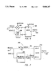
- FIG. 1 is a simplified block diagram of apparatus which incorporates the invention
- FIG. 2 is a plot of a desired gamma correction transfer function
- FIG. 3 is a block diagram of part of the gamma correction unit of FIG. 1;
- FIG. 4 is a block diagram of the mapping circuitry of FIG. 3;
- FIGS. 5, 6 and 7 are block diagrams of various implementations of the conversion circuitry of FIG. 3;
- FIG. 8 is a block diagram of the de-mapping circuitry of FIG. 3;
- FIG. 9 is a block diagram of another embodiment of the invention.
- FIGS. 10 and 11 are plots useful for explaining FIG. 9.
- the embodiments described herein illustrate how the invention can be used to implement one example of such a transfer function, specifically a gamma correction function.
- the gamma correction function is ratiometrically self-similar since, if the input value range is divided into logarithmically increasing sized segments, any segment of the curve can be made precisely congruent with any other segment of the curve if the two segments are separately bounded by rectangles having their lower left and upper right corners located on the curve, and the smaller rectangle and curve portion expanded independently in the x and y dimensions to the same respective size as the larger rectangle.
- FIG. 1 is a simplified block diagram of a color television system which incorporates the invention, showing components beginning with a source 102 of image data and ending with a human observer 104.
- Image data is provided to gamma correction circuitry 106 in the form of three digital streams carrying R, G and B signals.
- a single RGB triple is provided for each pixel to be displayed on a picture tube 108, the RGB triples being provided in a predetermined sequence corresponding to the horizontal and vertical scans of an electron beam (not shown) in the picture tube 108 against a phosphor backing 110.
- the gamma correction unit 106 performs gamma correction in the manner hereinafter described, separately on each value in each RGB triple.
- the gamma-corrected signals R.sub. ⁇ , G.sub. ⁇ and B.sub. ⁇ are coupled to a video encoder 112 which modulates the color information onto a color subcarrier, adds audio and synch information, and RF modulates the resulting signal for transmission via a sending antenna 114 to a receiving antenna 116.
- the composite signal may be transmitted via cable, the RF modulation being optionally omitted.
- the signal from antenna 116 is provided in a receiver to a video decoder 118 which receives the gamma-corrected triples R.sub. ⁇ G.sub. ⁇ B.sub. ⁇ for each pixel of incoming information. These values are converted to analog voltage signals and applied to control the beam energy of the electron beam in picture tube 108 at appropriate positions along the beam's scan of the phosphor 110.
- the light output L from the phosphor is not linearly related to the analog voltage applied to the beam, but rather, as previously described, follows a power function of L ⁇ E v .sup. ⁇ .
- the picture tube's conversion from gamma-corrected RGB values back to linear RGB values is shown symbolically in FIG. 1 as 120.
- FIG. 2 is a plot of the gamma correction transfer function used in the gamma correction unit 106 (FIG. 1).
- the gamma correction transfer function is identical for each of the three colors, red, green and blue, and the circuitry within the gamma correction unit 106 may in fact be multiplexed such that all three conversions are performed by a single circuit.
- the input value range spans 0.0-1.0.
- the portion 204 of the input value range is conceptually divided into ratiometrically increasing size segments. Specifically, except for the segment 210, the portion of the input value range occupied by each segment is twice the portion occupied by the next lower order segment. That is, segment 210 occupies one-sixteenth of the range; segment 212 occupies one-eighth of the range; segment 214 occupies one-quarter of the range; and segment 216 occupies one-half of the range. Stated another way, if the segments are numbered from the high-order segment 216 down toward the lowest order segment 210 for which the power curve 204 is used, then the portion of the input value range occupied by each segment is given by 2 -n . Stated yet another way, the segments can be numbered from the high-order segment 216 toward the low-order segment 210 by the negative log 2 of the proportion of the input value range which each segment occupies.
- FIG. 3 is an overall block diagram of an embodiment of circuitry used to implement the gamma correction for one of the color values R, G or B.
- the color values are represented in binary as eight physical signals arriving on the 8-bit X bus 302.
- the logic levels provided on the eight lines of the bus are considered a binary representation of a value between 0 and 255 inclusive, divided by 256.
- the gamma-corrected output values R.sub. ⁇ , G.sub. ⁇ or B.sub. ⁇ produced as outputs of the circuitry of FIG. 3 are represented on a Y bus 304 in binary as electrical signals carried on nine lines.
- the circuitry of FIG. 3 converts input physical signals to output physical signals according to the gamma correction techniques described herein.
- phrases such as "mapping a value” are to be read merely as a shorthand way of defining the physical steps of receiving signals representing the value, performing a manipulation on the signals which corresponds to the mapping function, and generating physical output signals representing the mapped result. Similar phrases calling for other mathematical manipulations are to be interpreted similarly.
- the present invention deals with physical entities such as physical signals that represent various numeric values, and signal processing hardware that inputs, processes and outputs such physical signals, as well as image data signals which ultimately cause a physical light image to be rendered on a display and observed by a viewer.
- the circuitry includes three primary functional units which correspond to the three primary steps of the gamma correction procedure.
- the RGB data input is provided first to mapping circuitry 306, which maps the input value represented on the X bus 302 to a mapped value which is within a standard segment of the input value range.
- the standard segment is advantageously chosen as the high-order segment 216.
- the mapped value is represented on a 7-bit DN bus 312, a high-order eighth bit of logic 1 being assumed as a matter of the definition of interactions between priority encoder 316 and mapping circuitry 306.
- the high-order eighth bit of logic 1 can be assumed since all of the mapped values are within the standard segment, and all of the x values within the standard segment have a high-order bit of logic 1.
- the mapped value on the DN bus 312 is provided to conversion circuitry 308, which converts the mapped value according to the gamma correction transfer function within the standard segment 216, as if the mapped value was an original input value.
- Conversion circuitry 308 produces a converted value represented on a 9-bit DS bus 314. The additional bit of precision is desirable because of the relative flatness of the gamma correction transfer function within the standard segment 216. If only 8 bits were produced by conversion circuitry 308, then the relative flatness of the transfer function would cause multiple instances of a given converted value in response to differing mapped values.
- the converted value represented on DS bus 314 is provided to de-mapping circuitry 310, which maps the converted value back to the original input value segment.
- the output of de-mapping circuitry 310 represents the R.sub. ⁇ , G.sub. ⁇ or B.sub. ⁇ gamma-corrected data output, and is represented in binary on the nine bits of the Y bus 304.
- the apparatus of FIG. 3 also includes a priority encoder 316 which determines which input value segment includes each input value on the X bus 302.
- the function of the priority encoder 316 may be considered as being part of either the mapping circuitry 306 or the de-mapping circuitry 310, or both, since its output is used by both.
- the priority encoder 316 receives as input the high-order four bits X(7:4) of the X bus 302, and drives a 5-bit N output bus 318.
- mapping circuitry 306 All five bits of the N bus 318 are provided to demapping circuitry 310. Since the output of mapping circuitry 306 is eventually ignored if the input value was in the special treatment segment 208, only bits N(3:0) are provided to mapping circuitry 306.
- FIG. 4 is a block diagram of mapping circuitry 306, showing its implementation as a mere barrel shifter 402. As previously described, since the segmentation of the input value range has been chosen in a geometric or log 2 fashion, mapping an input value into the standard segment 216 (FIG. 2) involves merely multiplying the input value by 2 n , where n is the number of bits between X(7) and the highest order bit of X(7:0) which contains a logic 1.
- the low-order seven bits of the X bus 302 are provided to the shifter 402 with the high-order bit, X(7), ignored.
- N(3:0) is also provided to the shifter 402.
- the shifter 402 itself is made up of a plurality of data selectors in a conventional manner, which select one of four differently shifted versions of X(6:0) onto the DN(6:0) output bus 312 in response to the four respective signals on N(3:0).
- the conversion circuitry 308 may be implemented as a ROM having seven address inputs and nine data outputs for a total of 1152 cells. This is shown in FIG. 5, in which the DN(6:0) bus-312 is provided to the address inputs of a memory 502, the Q outputs of which drive the DS(8:0) bus 314. This is only half the size of a conventional gamma correction ROM supporting equivalent input and output precision. Note that if it is desired to support more than one gamma correction transfer curve in gamma correction unit 106 (FIG. 1), such as by supporting user-selectable values of ⁇ , then the memory 502 can be made a random access memory. New conversion values for the standard segment 216 can then be downloaded to the memory 502 if the user selects a different value of ⁇ .
- ⁇ is not selectable, however, and in accordance with another aspect of the invention, the conversion is performed algorithmically rather than by look-up.
- the portion of the gamma correction transfer function which is within the standard segment 216 is linearly approximated by the equation
- the value on DN bus.312 has already been reduced by 0.5 due to the earlier stripping of the high-order logic 1.
- the seven remaining bits of the DN bus are provided to the multiplicand input of a multiplication circuit 602, and the multiplier input is connected to receive a fixed binary 137 (which is interpreted as 137/256 ⁇ 0.536).
- the output of multiplication circuitry 602 is provided to an A input of an adder 604, the B input of which is connected to receive a binary 187 (which is interpreted as 187/256 ⁇ 0.73).
- a small correction ROM 606 is provided which receives the seven bits of the DN bus 312 as an address input, and provides a 3-bit output to a C input of adder 308.
- the Q output of adder 604 drives the DS(8:0) bus 314.
- the ROM 606 is only three bits wide since it has been determined that only three bits of low-order correction information are necessary to correct for the deviation of the straight line approximation from the actual gamma correction curve within the standard segment 216. Furthermore, it has been determined that three low-order bits of correction information are still sufficient even if the value of m provided to multiplication circuitry 602 is reduced to 136/256, a value which permits multiplication circuitry 602 to be implemented extremely sparsely.
- multiplication of a mapped value by 136 is equivalent to multiplication by 128 plus multiplication by 8, which can be implemented merely by adding a seven-bit-left-shifted version of the multiplicand to a three-bit-left-shifted version of the multiplicand.
- FIG. 6 reduces the chip area to be occupied by the conversion circuitry 308 (FIG. 3) significantly below even that of the half-size ROM 502 in FIG. 5.
- FIG. 7 shows a particularly advantageous implementation for conversion circuitry 308.
- the multiplication circuitry 602 becomes merely a division by two which can be implemented with no hardware at all. That is, the 7-bit DN bus 312 is coupled to the A input of adder 604, but with each wire moved to the next less significant bit of the A input port.
- the low-order bit DN(0) is preferably not discarded, but rather maintained in the adder 604 to provide an additional bit of precision on the DS bus 314 output.
- the embodiment of FIG. 7 incorporates the b term into FIG. 7's equivalent of correction ROM 606, thereby widening the ROM to eight bits. But the embodiment also reduces the resolution of the correction ROM by a factor of four, leaving only 32 words of eight bits each.
- two 0 bits are concatenated as high-order bits to the DN(6:0) bus 312 to provide a 9-bit DA(8:0) bus 702 which is provided to the A input port of a 9-bit, 2-input adder 704.
- the concatenation of two high-order 0 bits corresponds to a right-shift of the mapped value on the DN bus by one bit, without discarding the low-order bit, and the increase in precision from seven to nine bits of precision.
- Bits 6:2 of the DN bus 312 are also provided to a non-linearity corrector 706, which provides an 8-bit output Q(7:0).
- Non-linearity corrector 706 is analogous to the correction ROM 606 (FIG. 6), but is preferably implemented using combinational logic since the values stored therein are such as to render such an implementation significantly smaller than the equivalent ROM.
- Table II sets forth the truth table of nonlinearity corrector 706; the primary advantage to a combinational implementation derives from the fact that all the output values in Q(6) are identical to those in both Q(5) and Q(4), and merely complementary to those in Q(7).
- Q(7:0) is concatenated with a high-order logic 1 to provide a DB(8:0) value to the 9-bit B input port of the adder 704.
- the adder 704 is conventional, though some simplifications may be possible since the high-order bits of the A and B input values are known and fixed.
- the implementation of FIG. 7 for conversion circuitry 308 is extremely compact.
- the de-mapping circuitry 310 (FIG. 3) performs a mapping of the converted value on the DS bus 314 back to the segment from which the mapped input value derived.
- de-mapping involves simply a multiplication of the converted value by a scale factor which depends only on the input value segment. Additionally, if the input segment is the special treatment segment 208, then the converted value on the DS bus 314 is ignored and the input value on the X bus 302 is merely multiplied by 4.6.
- the multiplication by the scale factors is implemented using a sparse multiplier involving only a few data selectors and a 3-input adder.
- the scale factor is unity. If the input value was within the input segment 14, then the scale factor is given by the ratio of the height of the rectangle bounding segment 214 to the height of the rectangle bounding standard segment 216. That is, the scale factor for input values which were within input value segment 214 is:
- Table III sets forth these scale factors for the various input value segments 210, 212, 214 and 216, together with their preferred sparse implementation in de-mapping circuitry 310.
- the sparse implementation of the special treatment input segment 208 is also shown and made a part of the sparse multiplier. As shown in FIG. 3, only the low-order four bits of the input value on the X bus 302 are provided to the de-mapping circuitry 310, since they are used only if the input value was within the special treatment input segment 208 and since all higher order bits of X must be zero in order for the input value to be within the special treatment input segment 208.
- FIG. 8 is a block diagram of the sparse multiplier which forms demapping circuitry 310. It comprises three data selectors 802, 804 and 806, each of which have two input ports and a control port. The first input port of each of the data selectors 802,804 and 806 receives DS and the second input port receives X. Each data selector can select differently shifted (and in one case complemented) versions of its input port values to its output.
- data selector 802 has four control inputs C(3:0).
- C3 is connected to receive the NL line from N-bus 318
- C2 is connected to receive the N3 line from N-bus 318.
- C1 is connected to the output of an OR gate 808, the two inputs of which are connected to receive N1 and N2, respectively.
- the C0 input of data selector 802 is connected to receive the N0 line from N-bus 318.
- data selector 802 passes DS(8:0) to its output port shifted right by 0 bits, i.e. unchanged.
- the output port of data selector 802 is 10 bits wide, and drives a bus designated S1(8:0, Z).
- Bits (8:0) of the S1 bus carry the same binary weight as respectively numbered bits on the DS bus 314 and (to the extent they exist) on X-bus 302.
- the bit line S1Z has a binary weight equal to half of the weight of bit line S10, and is provided to retain one additional bit of precision that would otherwise be lost as a result of right-shifts of a value on one of the input ports.
- data selector 802 sets S1Z to 0.
- mapping S1 2 -1 DS.
- Data selector 804 has a three-bit control port C(2:0).
- the C2 input is connected to receive NL, and the C1 input is connected to receive N2.
- the C0 input is connected to the output of an OR gate 810, the two inputs of which are connected to receive N1 and N3.
- the output port SA of data selector 804 drives a 10-bit wide SA bus, the lines of which are numbered SA (8:0, Z) . Values on the SA bus are interpreted in the same manner as those on the S1 bus.
- SA transformation
- Data selector 806 has a 4-bit control port C(3:0), which are connected to receive NL, N3, N2 and N1, respectively.
- the output port SB(4:0, Z) is only six bits wide, since the higher-order bits are always zero for all the shifted data selection options which data selector 806 can perform.
- the first input port of data selector 806 receives only DS(8:3), since the lower-order bits DS(2:0) are always shifted out and lost.
- X0 is not provided to data selector 806.
- SA(8:0, Z) are connected to respective A(8:0, Z) lines of an A input port of an adder 812.
- SB(4:0, Z) are similarly connected to respective B (4:0, Z) lines of a B input port of adder 812.
- B(8:5) of the B input port of adder 812 are connected to receive a logic zero.
- the carry input Ci of adder 812 is connected to receive N1 which comes in at the same binary weight as the Z bits.
- Adder 812 has a 9-bit output port SS(8:0) plus carry. Both the carry output and SS0 are ignored.
- the bits SS(8:0) have the same weight as respectively numbered bits on the SA bus and, to the extent they exist, on the SB bus.
- SAZ and SBZ are not used to form an SSZ output bit, but they are used to generate a carry signal for higher-order bits generated in the adder 812.
- the carry input Ci of adder 812 completes the two's complement negation begun in data selector 806 if N1 is active.
- the S1(8:0, Z) output lines from data selector 802 are connected to respective A(8:0, Z) lines of an A input port of another adder 814.
- the B7 and B8 inputs of adder 814 are connected to receive a logic zero, and the carry input Ci of adder 814 is connected to receive a logic one.
- the input value segment as represented on the N-bus 318 is used to select specific transformations in data selectors 802, 804 and 806, to produce values on buses S1, SA and SB.
- the values on buses SA and SB are added together by adder 812 and, if N1 is asserted, incremented by one. Since the input segment indicated by N1 is the only segment for which the demapping function requires a subtraction, N1 correctly indicates when adder 812 should increment its result by one to effect two's complement negation.
- the output of adder 812 is provided on SS bus, which is effectively divided by four as it is renamed S2.
- Adder 814 adds the value on the S1 bus and the value on the S2 bus, rounds to nine bits of precision, and provides the output of demapping circuitry 310 on Y-bus 304.
- Table IV sets forth the values on each of the buses in FIG. 8 for each of the possible values of N, thereby illustrating how the output values are arrived at on the Y-bus 304. It can be seen that the functions shown in Table IV for Y-bus 304 are the same as those listed in Table III.
- aspects of the invention can be implemented in software as well as hardware.
- the program includes a routine CalcGamma, which takes the input value (normalized to lie in the range [0.255]) as a parameter and returns the corresponding gamma corrected value (normalized to lie in the range [0.256]).
- the routine also prints intermediate results produced by the calculations, for the purposes of illustration. It will be understood that the printing of intermediate results can be omitted in a practical embodiment.
- the routine itself basically tracks the hardware embodiment described above.
- the CalcGamma routine can be modified in a manner apparent to a person of ordinary skill to omit outputting of intermediate results, and then compiled for execution on a microprocessor which would replace gamma correction unit 106 in the system of FIG. 1.
- Table V below is the output of the above computer program. The titles of the columns have been changed to more clearly indicate what they represent, and the output has been re-formatted as table. As can be seen, the calculation error is extremely small, especially for the portion 204 of the gamma correction curve (FIG. 2) which is not linearly approximated. This Table also serves to illustrate the accuracy of the hardware embodiment described with respect to FIGS. 3, 4, 5, 7 and 8.
- FIG. 9 is a block diagram illustrating another embodiment of the invention.
- the uncorrected input value X is provided to a true gamma corrector circuit 902, such as that illustrated in FIG. 3.
- the output Y of the true gamma corrector circuit 902 is provided to one input of a weighted averager 904, the other input of which receives the input value X.
- a weight signal W is also provided to the weighted averager 904, which produces an overall output signal Y given by
- W can be provided, for example, by leads on an integrated circuit package which the user can tie to fixed signal levels, or can be provided by a register which other circuitry can program with a desired value.
- curve 1004 represents the uncorrected input value X
- curve 1012 represents the weighted average function
- FIG. 11 is a computer-generated plot illustrating the same results as FIG. 10, except that the true gamma correctors 902 approximate the low-order 1/16 of the input compliance range with straight lines (see portion 206 in the plot of FIG. 2).
- curve 1104 represents the uncorrected input value X
- curve 1112 represents the weighted average function
- apparatus can also be designed in which choices are made available for W which are outside the range of [0,1], to thereby further extend the flexibility of the device.
- Apparatus can be designed also in which the function implemented by the 3-step circuitry does not exactly match any power law function, an exact (or more nearly exact) match being achieved only when an intermediate value is selected for W.
Abstract
Description
L∝E.sub.v.sup.γ.
y'=C+mx',
m=[y(x.sub.s1)-y(x.sub.s0)] / (x.sub.s1 -x.sub.s0),
x'=2.sup.n x-x.sub.s0, and
y'=C+mx'+F(x'),
K=[y(x.sub.i1)-y(x.sub.i0)]/[y(x.sub.s1)-y(x.sub.s0)]
y=W.sub.1 y+W.sub.2 x+W.sub.3,
TABLE I ______________________________________ PRIORITYENCODER X N Segment 7 6 5 4 3 2 1 0 3 2 1 0 L Identified ______________________________________ 1d d d d d d d 0 0 0 1 0 216 0 1d d d d d d 0 0 1 0 0 214 0 0 1d d d d d 0 1 0 0 0 212 0 0 0 1d d d d 1 0 0 0 0 210 0 0 0 0d d d d 0 0 0 0 1 208 ______________________________________
y=mx'+b,
m=[y(1.0)-y(0.5)]/(1.0-0.5)=0.536≈137/256, and
b=y(0.5)=0.73≈187/256.
              TABLE II
______________________________________
NON-LINEARITY CORRECTOR
DN(6:2)             Q(7:0)
______________________________________
0   0     0      0   0        0   1   1   1   0   1
                          1   1
                          0   0     0 0 1  0 1 1 1 1 0 0 0
                          0   0     0 1 0  0 1 1 1 1 0 0 1
                          0   0     0 1 1  0 1 1 1 1 0 1 0
                          0   0     1 0 0  0 1 1 1 1 0 1 1
                          0   0     1 0 1  0 1 1 1 1 1 0 0
                          0   0     1 1 0  0 1 1 1 1 1 0 1
                          0   0     1 1 1  0 1 1 1 1 1 1 0
                          0   1     0 0 0  0 1 1 1 1 1 1 0
                          0   1     0 0 1  0 1 1 1 1 1 1 1
                          0   1     0 1 0  1 0 0 0 0 0 0 0
                          0   1     0 1 1  1 0 0 0 0 0 0 0
                          0   1     1 0 0  1 0 0 0 0 0 0 1
                          0   1     1 0 1  1 0 0 0 0 0 0 1
                          0   1     1 1 0  1 0 0 0 0 0 0 1
                          0   1     1 1 1  1 0 0 0 0 0 1 0
                          1   0     0 0 0  1 0 0 0 0 0 1 0
                          1   0     0 0 1  1 0 0 0 0 0 1 0
                          1   0     0 1 0  1 0 0 0 0 0 1 0
                          1   0     0 1 1  1 0 0 0 0 0 1 0
                          1   0     1 0 0  1 0 0 0 0 0 1 0
                          1   0     1 0 1  1 0 0 0 0 0 1 0
                          1   0     1 1 0  1 0 0 0 0 0 1 0
                          1   0     1 1 1  1 0 0 0 0 0 1 0
                          1   1     0 0 0  1 0 0 0 0 0 1 0
                          1   1     0 0 1  1 0 0 0 0 0 1 0
                          1   1     0 1 0  1 0 0 0 0 0 1 0
                          1   1     0 1 1  1 0 0 0 0 0 1 0
                          1   1     1 0 0  1 0 0 0 0 0 0 1
                          1   1     1 0 1  1 0 0 0 0 0 0 1
                          1   1     1 1 0  1 0 0 0 0 0 0 1
                          1   1     1 1 1  1 0 0 0 0 0 0 0
______________________________________
[y(0.5)-y(0.25)]/[y(1.0)-y(0.5)]=0.732≈376/512.
[y(0.25)-y(0.125)]/[y(1.0)-y(0.5)]=0.536≈274/512.
[y(0.125)-y(0.0625)]/[y(1.0)-y(0.5)]=0.392≈200/512.
TABLE III ______________________________________ DE-MAPPING CIRCUITRY Input Seg- Scale ment N(3:0,L) Factor Sparse Implementation ______________________________________ 216 00010 512/512 Y =DS 214 00100 376/512 Y = (2.sup.8 DS + 2.sup.7 DS - 2.sup.3 DS)/512 212 01000 274/512 Y = (2.sup.8 DS + 2.sup.4 DS + 2.sup.1 DS)/512 210 10000 200/512 Y = (2.sup.7 DS + 2.sup.6 DS + 2.sup.3 DS)/512 208 00001 N/A Y = (2.sup.2 X + 2.sup.-1 X + 2.sup.-3 X) ______________________________________
                                  TABLE IV
__________________________________________________________________________
N   S1   SA   SB         SS = SA + SB + 2.sup.-10 N1
                                         S2 = 2.sup.-2 SS
                                                  Y = S1 + S2
__________________________________________________________________________
                                                  (rounded)
N0  DS   0    0          0               0        DS
                         (DS - 2.sup.-4 DS - 2.sup.-10 + 2.sup.-10)
                                                  (2.sup.-1 + 2.sup.-2 -
                                                  2.sup.-6)DS
N1  2.sup.-1 DS
         DS   (-2.sup.-4 DS - 2.sup.-10) (2.sup.-2 - 2.sup.-6)DS
                         = (1 - 2.sup.-4)DS       = 0.734375DS
                                                  (2.sup.-1 + 2.sup.-5 +
                                                  2.sup.-8)DS
N2  2.sup.-1 DS
         2.sup.-3 DS
              2.sup.-6 DS
                         (2.sup.-3 + 2.sup.-6)DS
                                         (2.sup.-5 + 2.sup.-8)DS
                                                  = 0.535156DS
                                                  (2.sup.-2 + 2.sup.-3 +
                                                  2.sup.-6)DS
N3  2.sup.-3 DS
         DS   2.sup.-4 DS
                         (1 + 2.sup.-4)DS
                                         (2.sup.-2 + 2.sup.-6)DS
                                                  = 0.390625DS
                                                  (2.sup.2 + 2.sup.-1 +
                                                  2.sup.-3)X
NL  S.sup.2 X
         2.sup.1 X
              2.sup.-1 X (2.sup.1 + 2.sup.-1)X
                                         (2.sup.-1 + 2.sup.-3)X
                                                  = 4.625X
__________________________________________________________________________
__________________________________________________________________________
/* a C language routine to calculate a gamma corrected dat
*/lue
/* passed parameter is input data, return value is gamma corrected
*/ta
/* By David Main, 181 Oak Knoll Dr. Boulder Creek, CA., May 17,
*/93
/* Copyright © 1993 The 3DO Company - All rights
*/served
/* ***********************************************************************
************* */
/* Defines, Declarations, Includes, and Function Prototypes
*/
#include <stdio.h>
#include <stdlib.h>
#include <conio.h>
#include <math.h>
#define uchar unsigned char
/* abreviate reserved word syntax */
#define uint unsigned int
/* abreviate reserved word syntax */
#define Gamma 2.2
/* define the gamma value being corrected for */
float GamCor
;/* gamma correction factor */
float Kgamma
;/* true gamma correction calculation factor */
uint Data ;/* data variable */
uchar CalcGamma(uchar Input.sub.-- Value)
;/* gamma correction function */
/* ***********************************************************************
************* */
/* ***
START OF PROGRAM EXECUTION *** */
int main() {
printf(" nGamma Corrector Method Demonstration Program
nBy David Main for The 3DO Company. Boulder Creek, CA. May 18, 1993.
nAll rights reserved. n n") ;
GamCor = 1/Gamma
;/* calculate the reciprocal correction factor */
Kgamma = 256.0 * pow(256,-GamCor)
;/* true gamma correct value factor */
/* data format header line # 1 */
printf("
nInput t Shift tMapped tLinear tSub- tNon- tStd tOutput tTrue tCalc") ;
/* data format header line # 2 */
printf("
nData t Bits tData tTerm tSeg tLinear tSeg tData tValue tError") ;
for (Data = 0 ; Data < 256 ; Data + + )
CalcGamma(Data) ;
printf(" nEnd of Demonstration n") ;
return(0) ;
/* ***********************************************************************
************* */
/* Receive source data value. Return with gamma corrected value. Data is
in */
/* the range of 0×00 through 0×FF (0 through 255). The
function performed */
/* is: */
/* Return.sub.-- value = Input.sub.-- Value GamCor
*/
/* */
/* where " GamCor" is the gamma correction factor.
*/
uchar CalcGamma(uchar Input.sub.-- Value) {
uchar Mapped.sub.-- Value
;/* declare input value mapped to standard segment */
uchar n
;/* binary power factor to map input data into standard segment */
uint Linear
;/* linear approximation term in standard segment */
uint Non.sub.-- Linear
;/* non-linear approximation term in standard segment */
uint Sub.sub.-- Segment
;/* non-linear approximation sub-segment */
uint Standard.sub.-- Seg
;/* standard segment calculated value */
uint Output.sub.-- Value
;/* gamma corrected output value */
uint Real.sub.-- Value
;/* theoretical true gamma corrected value */
/* ***
MAP THE INPUT DATA INTO THE STANDARD SEGMENT
*** */
Mapped.sub.-- Value = Input.sub.-- Value
;/* keep input data. Operate on a copy of it */
printf(" n%u",Input.sub.-- Value)
;/* report source data to console */
if (Mapped.sub.-- Value & 0×F0)
/* do mapping if input 4 MSB's are not all 0 */
for ( n = 0 ; (Mapped.sub.-- Value & 0×80) = = 0 ; n
/* loop to find "n" */
Mapped.sub.-- Value = Mapped.sub.-- Value < < 1
;/* shift up one bit */
else
n = 4 ;/* flag linear function approximation segment */
Mapped.sub.-- Value = Mapped.sub.-- Value & 0×7F
;/* be gone, a-priori MSB always 1 */
printf(" t%u",n)
;/* report mapping shift count to console */
printf(" t%u",Mapped.sub.-- Value)
;/* report mapped data value to console */
/* **
CALCULATE THE LINEAR AND NON-LINEAR APPROXIMATION TERMS
** */
Linear = Mapped.sub.-- Value < < 0
;/* normalize from 8 to 10 bits & divide by 2 */
printf(" t%d",Linear)
;/* report linear approximation term to console */
/* The non-linear approximation is performed by dividing the curve
in the standard segment into 32 equal sub-segments, each of
which is given a non-linear correction value by table lookup. The
approximation sub-segment is conveniently determined by
shifting the Mapped.sub.-- Value right by two bits.
*/
Sub.sub.-- Segment = Mapped.sub.-- Value > > 2
;/* approximation sub segment */
printf(" t%d",Sub.sub.-- Segment)
;/* report sub-segment to console */
switch (Sub.sub.-- Segment) {
case (0) : Non.sub.-- Linear = 375 ; break ;
case (1) : Non.sub.-- Linear = 376 ; break ;
case (2) : Non.sub.-- Linear = 377 ; break ;
case (3) : Non.sub.-- Linear = 378 ; break ;
case (4) : Non.sub.-- Linear = 379 ; break ;
case (5) : Non.sub.-- Linear = 380 ; break ;
case (6) : Non.sub.-- Linear = 381 ; break ;
case (7) : Non.sub.-- Linear = 382 ; break ;
case (8) : Non.sub.-- Linear = 382 ; break ;
case (9) : Non.sub. -- Linear = 383 ; break ;
case (10) : Non.sub.-- Linear = 384 ; break ;
case (11) : Non.sub.-- Linear = 384 ; break ;
case (12) : Non.sub.-- Linear = 385 ; break ;
case (13) : Non.sub.-- Linear = 385 ; break ;
case (14) : Non.sub.-- Linear = 385 ; break ;
case (15) : Non.sub.-- Linear = 386 ; break ;
case (16) : Non.sub.-- Linear = 386 ; break ;
case (17) : Non.sub.-- Linear = 386 ; break ;
case (18) : Non.sub.-- Linear = 386 ; break ;
case (19) : Non.sub.-- Linear = 386 ; break ;
case (20) : Non.sub.-- Linear = 386 ; break ;
case (21) : Non.sub.-- Linear = 386 ; break ;
case (22) : Non.sub.-- Linear = 386 ; break ;
case (23) : Non.sub.-- Linear = 386 ; break ;
case (24) : Non.sub.-- Linear = 386 ; break ;
case (25) : Non.sub.-- Linear = 386 ; break ;
case (26) : Non.sub.-- Linear = 386 ; break ;
case (27) : Non.sub.-- Linear = 386 ; break ;
case (28) : Non.sub.-- Linear = 385 ; break ;
case (29) : Non.sub.-- Linear = 385 ; break ;
case (30) : Non.sub.-- Linear = 385 ; break ;
case (31) : Non.sub.-- Linear = 384 ; break ;
}
printf(" t%u",Non.sub.-- Linear)
;/* report non-linear term to console */
/* ***
SUM THE LINEAR AND NON-LINEAR APPROXIMATION TERMS
*** */
Standard.sub.-- Seg = Linear + Non.sub.-- Linear
;/* sum linear and non-linear term */
printf(" t%u",Standard.sub.-- Seg)
;/* report standard segment value to console */
/* ***
DE-MAP THE STANDARD SEGMENT VALUE *** */
switch (n) {
case 0 : Output.sub.-- Value
/* input was native to standard segment */
= Standard.sub.-- Seg
;/* Kdemap = 1.0 */
break ;
case 1 : Output.sub.-- Value
/* input was native to standard segment - 1 */
= (Standard.sub.-- Seg > > 1)
+ (Standard.sub.-- Seg > > 2)
- (Standard.sub.-- Seg > > 6)
;/* Kdemap = 0.734375 */
break ;
case 2 : Output.sub.-- Value
/* input was native to standard segment - 2 */
= (Standard.sub.-- Seg > > 1)
+ (Standard.sub.-- Seg > > 5)
+ (Standard.sub.-- Seg > > 8)
;/* Kdemap = 0.535156 */
break ;
case 3 : Output.sub.-- Value
/* input was native to standard segment - 3 */
= (Standard.sub.-- Seg > > 2)
+ (Standard.sub.-- Seg > > 3)
+ (Standard.sub.-- Seg > > 6)
;/* Kdemap = 0.390625 */
break ;
case 4: Output.sub.-- Value
/* input was less than 16 */
= (Input.sub.-- Value < < 3)
+ (Input.sub.-- Value > > 0)
+ (Input.sub.-- Value > > 2)
;/* Kdemap = 4.625 */
break ;
}
Output.sub.-- Value = (Output.sub.-- Value + 1)/2
;/* round off, normalize to 8 bits */
printf(" t%u",Output.sub.-- Value)
;/* report gamma corrected data to console */
Real.sub.-- Value = ((Kgamma * pow(Input.sub.-- Value,GamCor))
;/* true value */
printf(" t%d", Real.sub.-- Value)
;/* report true value to console */
printf(" t%d", Output.sub.-- Value - Real.sub.-- Value)
;/* report calc err to console */
return(Output.sub.-- Value) ;
}
/* end of demonstration program listing */
__________________________________________________________________________
                                  TABLE V
__________________________________________________________________________
                 Standard Segment Conversion
                                     De-  Accuracy
Mapping               Aprxn
                           Non- Total
                                     map  comparison
Input
     Shift bits
           Mapped
                 Linear
                      sub- linear
                                cnvt'd
                                     Output
                                          True Calc
value
     (N)   value term seg  term value
                                     value
                                          value
                                               error
__________________________________________________________________________
0    4     0     0    0    375  375  0    0    0
1    4     1     1    0    375  376  5    21   -16
2    4     2     2    0    375  377  9    28   -19
3    4     3     3    0    375  378  14   34   -20
4    4     4     4    1    376  380  19   39   -20
5    4     5     5    1    376  381  23   43   -20
6    4     6     6    1    376  382  28   46   -18
7    4     7     7    1    376  383  32   50   -18
8    4     8     8    2    377  385  37   53   -16
9    4     9     9    2    377  386  42   56   -14
10   4     10    10   2    377  387  46   59   -13
11   4     11    11   2    377  388  51   61   -10
12   4     12    12   3    378  390  56   64   -8
13   4     13    13   3    378  391  60   66   -6
14   4     14    14   3    378  392  65   68   -3
15   4     15    15   3    378  393  69   70   -1
16   3     0     0    0    375  375  72   73   -1
17   3     8     8    2    377  385  75   75   0
18   3     16    16   4    379  395  77   77   0
19   3     24    24   6    381  405  79   78   1
20   3     32    32   8    382  414  80   80   0
21   3     40    40   10   384  424  83   82   1
22   3     48    48   12   385  433  84   84   0
23   3     56    56   14   385  441  86   86   0
24   3     64    64   16   386  450  88   87   1
25   3     72    72   18   386  458  89   89   0
26   3     80    80   20   386  466  91   91   0
27   3     88    88   22   386  474  92   92   0
28   3     96    96   24   386  482  94   94   0
29   3     104   104  26   386  490  95   95   0
30   3     112   112  28   385  497  97   97   0
31   3     120   120  30   385  505  98   98   0
32   2     0     0    0    375  375  100  99   1
33   2     4     4    1    376  380  101  101  0
34   2     8     8    2    377  385  103  102  1
35   2     12    12   3    378  390  104  104  0
36   2     16    16   4    379  395  105  105  0
37   2     20    20   5    380  400  107  106  1
38   2     24    24   6    381  405  108  108  0
39   2     28    28   7    382  410  109  109  0
40   2     32    32   8    382  414  110  110  0
41   2     36    36   9    383  419  112  111  1
42   2     40    40   10   384  424  113  113  0
43   2     44    44   11   384  428  114  114  0
44   2     48    48   12   385  433  115  115  0
45   2     52    52   13   385  437  116  116  0
46   2     56    56   14   385  441  117  117  0
47   2     60    60   15   386  446  119  118  1
48   2     64    64   16   386  450  120  120  0
49   2     68    68   17   386  454  121  121  0
50   2     72    72   18   386  458  122  122  0
51   2     76    76   19   386  462  123  123  0
52   2     80    80   20   386  466  124  124  0
53   2     84    84   21   386  470  125  125  0
54   2     88    88   22   386  474  126  126  0
55   2     92    92   23   386  478  127  127  0
56   2     96    96   24   386  482  129  128  1
57   2     100   100  25   386  486  130  129  1
58   2     104   104  26   386  490  131  130  1
59   2     108   108  27   386  494  132  131  1
60   2     112   112  28   385  497  132  132  0
61   2     116   116  29   385  501  133  133  0
62   2     120   120  30   385  505  134  134  0
63   2     124   124  31   384  508  135  135  0
64   1     0     0    0    375  375  138  136  2
65   1     2     2    0    375  377  139  137  2
66   1     4     4    1    376  380  140  138  2
67   1     6     6    1    376  382  141  139  2
68   1     8     8    2    377  385  141  140  1
69   1     10    10   2    377  387  142  141  1
70   1     12    12   3    378  390  143  142  1
71   1     14    14   3    378  392  144  143  1
72   1     16    16   4    379  395  145  144  1
73   1     18    18   4    379  397  146  145  1
74   1     20    20   5    380  400  147  146  1
75   1     22    22   5    380  402  148  147  1
76   1     24    24   6    381  405  149  147  2
77   1     26    26   6    381  407  149  148  1
78   1     28    28   7    382  410  151  149  2
79   1     30    30   7    382  412  152  150  2
80   1     32    32   8    382  414  152  151  1
81   1     34    34   8    382  416  153  152  1
82   1     36    36   9    383  419  154  153  1
83   1     38    38   9    383  421  155  153  2
84   1     40    40   10   384  424  156  154  2
85   1     42    42   10   384  426  157  155  2
86   1     44    44   11   384  428  158  156  2
87   1     46    46   11   384  430  158  157  1
88   1     48    48   12   385  433  159  158  1
89   1     50    50   12   385  435  160  158  2
90   1     52    52   13   385  437  161  159  2
91   1     54    54   13   385  439  161  160  1
92   1     56    56   14   385  441  162  161  1
93   1     58    58   14   385  443  163  162  1
94   1     60    60   15   386  446  164  162  2
95   1     62    62   15   386  448  165  163  2
96   1     64    64   16   386  450  165  164  1
97   1     66    66   16   386  452  166  165  1
98   1     68    68   17   386  454  167  165  2
99   1     70    70   17   386  456  168  166  2
100  1     72    72   18   386  458  168  167  1
101  1     74    74   18   386  460  169  168  1
102  1     76    76   19   386  462  170  168  2
103  1     78    78   19   386  464  171  169  2
104  1     80    80   20   386  466  171  170  1
105  1     82    82   20   386  468  172  171  1
106  1     84    84   21   386  470  173  171  2
107  1     86    86   21   386  472  174  172  2
108  1     88    88   22   386  474  174  173  1
109  1     90    90   22   386  476  175  174  1
110  1     92    92   23   386  478  176  174  2
111  1     94    94   23   386  480  177  175  2
112  1     96    96   24   386  482  177  176  1
113  1     98    98   24   386  484  178  177  1
114  1     100   100  25   386  486  179  177  2
115  1     102   102  25   386  488  180  178  2
116  1     104   104  26   386  490  180  179  1
117  1     106   106  26   386  492  181  179  2
118  1     108   108  27   386  494  182  180  2
119  1     110   110  27   386  496  183  181  2
120  1     112   112  28   385  497  183  181  2
121  1     114   114  28   385  499  183  182  1
122  1     116   116  29   385  501  184  183  1
123  1     118   118  29   385  503  185  183  2
124  1     120   120  30   385  505  186  184  2
125  1     122   122  30   385  507  186  185  1
126  1     124   124  31   384  508  187  185  2
127  1     126   126  31   384  510  188  186  2
128  0     0     0    0    375  375  188  187  1
129  0     1     1    0    375  376  188  187  1
130  0     2     2    0    375  377  189  188  1
131  0     3     3    0    375  378  189  189  0
132  0     4     4    1    376  380  190  189  1
133  0     5     5    1    376  381  191  190  1
134  0     6     6    1    376  382  191  191  0
135  0     7     7    1    376  383  192  191  1
136  0     8     8    2    377  385  193  192  1
137  0     9     9    2    377  386  193  193  0
138  0     10    10   2    377  387  194  193  1
139  0     11    11   2    377  388  194  194  0
140  0     12    12   3    378  390  195  195  0
141  0     13    13   3    378  391  196  195  1
142  0     14    14   3    378  392  196  196  0
143  0     15    15   3    378  393  197  196  1
144  0     16    16   4    379  395  198  197  1
145  0     17    17   4    379  396  198  198  0
146  0     18    18   4    379  397  199  198  1
147  0     19    19   4    379  398  199  199  0
148  0     20    20   5    380  400  200  200  0
149  0     21    21   5    380  401  201  200  1
150  0     22    22   5    380  402  201  201  0
151  0     23    23   5    380  403  202  201  1
152  0     24    24   6    381  405  203  202  1
153  0     25    25   6    381  406  203  203  0
154  0     26    26   6    381  407  204  203  1
155  0     27    27   6    381  408  204  204  0
156  0     28    28   7    382  410  205  204  1
157  0     29    29   7    382  411  206  205  1
158  0     30    30   7    382  412  206  206  0
159  0     31    31   7    382  413  207  206  1
160  0     32    32   8    382  414  207  207  0
161  0     33    33   8    382  415  208  207  1
162  0     34    34   8    382  416  208  208  0
163  0     35    35   8    382  417  209  209  0
164  0     36    36   9    383  419  210  209  1
165  0     37    37   9    383  420  210  210  0
166  0     38    38   9    383  421  211  210  1
167  0     39    39   9    383  422  211  211  0
168  0     40    40   10   384  424  212  211  1
169  0     41    41   10   384  425  213  212  1
170  0     42    42   10   384  426  213  213  0
171  0     43    43   10   384  427  214  213  1
172  0     44    44   11   384  428  214  214  0
173  0     45    45   11   384  429  215  214  1
174  0     46    46   11   384  430  215  215  0
175  0     47    47   11   384  431  216  215  1
176  0     48    48   12   385  433  217  216  1
177  0     49    49   12   385  434  217  216  1
178  0     50    50   12   385  435  218  217  1
179  0     51    51   12   385  436  218  218  0
180  0     52    52   13   385  437  219  218  1
181  0     53    53   13   385  438  219  219  0
182  0     54    54   13   385  439  220  219  1
183  0     55    55   13   385  440  220  220  0
184  0     56    56   14   385  441  221  220  1
185  0     57    57   14   385  442  221  221  0
186  0     58    58   14   385  443  222  221  1
187  0     59    59   14   385  444  222  222  0
188  0     60    60   15   386  446  223  222  1
189  0     61    61   15   386  447  224  223  1
190  0     62    62   15   386  448  224  224  0
191  0     63    63   15   386  449  225  224  1
192  0     64    64   16   386  450  225  225  0
193  0     65    65   16   386  451  226  225  1
194  0     66    66   16   386  452  226  226  0
195  0     67    67   16   386  453  227  226  1
196  0     68    68   17   386  454  227  227  0
197  0     69    69   17   386  455  228  227  1
198  0     70    70   17   386  456  228  228  0
199  0     71    71   17   386  457  229  228  1
200  0     72    72   18   386  458  229  229  0
201  0     73    73   18   386  459  230  229  1
202  0     74    74   18   386  460  230  230  0
203  0     75    75   18   386  461  231  230  1
204  0     76    76   19   386  462  231  231  0
205  0     77    77   19   386  463  232  231  1
206  0     78    78   19   386  464  232  232  0
207  0     79    79   19   386  465  233  232  1
208  0     80    80   20   386  466  233  233  0
209  0     81    81   20   386  467  234  233  1
210  0     82    82   20   386  468  234  234  0
211  0     83    83   20   386  469  235  234  1
212  0     84    84   21   386  470  235  235  0
213  0     85    85   21   386  471  236  235  1
214  0     86    86   21   386  472  236  236  0
215  0     87    87   21   386  473  237  236  1
216  0     88    88   22   386  474  237  237  0
217  0     89    89   22   386  475  238  237  1
218  0     90    90   22   386  476  238  238  0
219  0     91    91   22   386  477  239  238  1
220  0     92    92   23   386  478  239  239  0
221  0     93    93   23   386  479  240  239  1
222  0     94    94   23   386  480  240  240  0
223  0     95    95   23   386  481  241  240  1
224  0     96    96   24   386  482  241  241  0
225  0     97    97   24   386  483  242  241  1
226  0     98    98   24   386  484  242  242  0
227  0     99    99   24   386  485  243  242  1
228  0     100   100  25   386  486  243  243  0
229  0     101   101  25   386  487  244  243  1
230  0     102   102  25   386  488  244  244  0
231  0     103   103  25   386  489  245  244  1
232  0     104   104  26   386  490  245  245  0
233  0     105   105  26   386  491  246  245  1
234  0     106   106  26   386  492  246  246  0
235  0     107   107  26   386  493  247  246  1
236  0     108   108  27   386  494  247  247  0
237  0     109   109  27   386  495  248  247  1
238  0     110   110  27   386  496  248  248  0
239  0     111   111  27   386  497  249  248  1
240  0     112   112  28   385  497  249  249  0
241  0     113   113  28   385  498  249  249  0
242  0     114   114  28   385  499  250  250  0
243  0     115   115  28   385  500  250  250  0
244  0     116   116  29   385  501  251  250  1
245  0     117   117  29   385  502  251  251  0
246  0     118   118  29   385  503  252  251  1
247  0     119   119  29   385  504  252  252  0
248  0     120   120  30   385  505  253  252  1
249  0     121   121  30   385  506  253  253  0
250  0     122   122  30   385  507  254  253  1
251  0     123   123  30   385  508  254  254  0
252  0     124   124  31   384  508  254  254  0
253  0     125   125  31   384  509  255  255  0
254  0     126   126  31   384  510  255  255  0
255  0     127   127  31   384  511  256  256  0
__________________________________________________________________________
Y=WY+(1-W)X.
Y=(X.sup.1/2.2 +X)/2.
Y=(X.sup.1/2.8 +X)/2.
Y=(X.sup.1/2.8 +X)/2.
Claims (57)
Priority Applications (3)
| Application Number | Priority Date | Filing Date | Title |
|---|---|---|---|
| US08/222,181 US5408267A (en) | 1993-07-06 | 1994-03-31 | Method and apparatus for gamma correction by mapping, transforming and demapping |
| PCT/US1994/007325 WO1995002299A1 (en) | 1993-07-06 | 1994-06-29 | Gamma correction for video encoder |
| AU73570/94A AU7357094A (en) | 1993-07-06 | 1994-06-29 | Gamma correction for video encoder |
Applications Claiming Priority (2)
| Application Number | Priority Date | Filing Date | Title |
|---|---|---|---|
| US8749093A | 1993-07-06 | 1993-07-06 | |
| US08/222,181 US5408267A (en) | 1993-07-06 | 1994-03-31 | Method and apparatus for gamma correction by mapping, transforming and demapping |
Related Parent Applications (1)
| Application Number | Title | Priority Date | Filing Date |
|---|---|---|---|
| US8749093A Continuation-In-Part | 1993-07-06 | 1993-07-06 |
Publications (1)
| Publication Number | Publication Date |
|---|---|
| US5408267A true US5408267A (en) | 1995-04-18 |
Family
ID=26777029
Family Applications (1)
| Application Number | Title | Priority Date | Filing Date |
|---|---|---|---|
| US08/222,181 Expired - Lifetime US5408267A (en) | 1993-07-06 | 1994-03-31 | Method and apparatus for gamma correction by mapping, transforming and demapping |
Country Status (3)
| Country | Link |
|---|---|
| US (1) | US5408267A (en) |
| AU (1) | AU7357094A (en) |
| WO (1) | WO1995002299A1 (en) |
Cited By (55)
| Publication number | Priority date | Publication date | Assignee | Title |
|---|---|---|---|---|
| US5537071A (en) * | 1993-11-23 | 1996-07-16 | U.S. Philips Corporation | Method and circuit for dividing an input signal into amplitude segment signals and for non-linearly processing the amplitude segment signals on the basis of the value of each amplitude segment signal |
| US5706058A (en) * | 1995-09-05 | 1998-01-06 | Sanyo Electric Co., Ltd. | Gamma correction circuit for correcting video data obtained by photoelectric transfer and having a non-linear characteristic |
| US5764216A (en) * | 1993-06-30 | 1998-06-09 | Fujitsu Limited | Gamma correction circuit, a liquid crystal driver, a method of displaying image, and a liquid crystal display |
| WO1999011070A1 (en) * | 1997-08-29 | 1999-03-04 | Logitech Inc. | Video capture and compression system and method for composite video |
| US5933199A (en) * | 1995-09-15 | 1999-08-03 | Lg Electronics Inc. | Gamma correction circuit using analog multiplier |
| US6026423A (en) * | 1996-03-29 | 2000-02-15 | Siemens Energy & Automation, Inc. | Fractional precision integer square root processor and method for use with electronic circuit breaker systems |
| US6137542A (en) * | 1998-12-21 | 2000-10-24 | Phillips Electronics North America Corporation | Digital correction of linear approximation of gamma |
| US6166781A (en) * | 1996-10-04 | 2000-12-26 | Samsung Electronics Co., Ltd. | Non-linear characteristic correction apparatus and method therefor |
| US6278496B1 (en) * | 1997-10-09 | 2001-08-21 | Sanyo Electric Co., Ltd. | Digital correction circuit and image data processing apparatus equipped with a digital correction circuit |
| US6587584B1 (en) * | 1999-06-28 | 2003-07-01 | Hyundai Electronics Industries Co., Ltd. | Apparatus for gamma correcting image data |
| US6633343B2 (en) * | 2000-03-14 | 2003-10-14 | Matsushita Electric Industrial Co., Ltd. | Dynamic gamma correction apparatus |
| US6707955B1 (en) * | 1999-06-30 | 2004-03-16 | Canon Kabushiki Kaisha | Image sensing device, image processing apparatus and method, and memory medium |
| US6791576B1 (en) | 2000-02-23 | 2004-09-14 | Neomagic Corp. | Gamma correction using double mapping with ratiometrically-related segments of two different ratios |
| US6795091B2 (en) | 2001-02-28 | 2004-09-21 | Samsung Electronics Co., Ltd. | Display apparatus and method for gamma correcting a video signal therein |
| US20040213457A1 (en) * | 2003-04-10 | 2004-10-28 | Seiko Epson Corporation | Image processor, image processing method, and recording medium on which image processing program is recorded |
| US20040252240A1 (en) * | 2003-04-02 | 2004-12-16 | Kabushiki Kaisha Toshiba | Nonlinear process circuit used for image processing |
| US20040268201A1 (en) * | 2003-06-30 | 2004-12-30 | Towfique Haider | Video correction system and method using logarithmic conversion |
| US20040267854A1 (en) * | 2003-06-26 | 2004-12-30 | Towfique Haider | Logarithmic and inverse logarithmic conversion system and method |
| US6917382B1 (en) * | 1999-07-27 | 2005-07-12 | Canon Kabushiki Kaisha | Signal processing apparatus and method thereof |
| US20060244849A1 (en) * | 2005-04-13 | 2006-11-02 | Sunplus Technology Co., Ltd. | Gamma correction method and system |
| US7154562B1 (en) * | 2003-10-14 | 2006-12-26 | Cirrus Logic, Inc. | Methods and circuits for implementing programmable gamma correction |
| US20070041661A1 (en) * | 2005-08-18 | 2007-02-22 | Hung Szepo B | Systems, methods, and apparatus for table construction and use in image processing |
| US20070104384A1 (en) * | 2005-11-08 | 2007-05-10 | Rodney Shaw | Apparatus and Methods for Enhancing Digital Images |
| US20070229712A1 (en) * | 2006-03-31 | 2007-10-04 | Sharp Kabushiki Kaisha | Digital gamma correction circuit and digital gamma correction method |
| CN100397448C (en) * | 2001-04-29 | 2008-06-25 | 中华映管股份有限公司 | Sectional grey scale compensating method of image input to planar plasma display |
| CN100411424C (en) * | 2005-04-18 | 2008-08-13 | 凌阳科技股份有限公司 | Gama correcting method and system |
| US20090027504A1 (en) * | 2007-07-25 | 2009-01-29 | Suk Hwan Lim | System and method for calibrating a camera |
| US20090027523A1 (en) * | 2007-07-25 | 2009-01-29 | Nelson Liang An Chang | System and method for determining a gamma curve of a display device |
| WO2010012083A1 (en) * | 2008-07-29 | 2010-02-04 | Ignis Innovation Inc. Et Al | Method and system for driving light emitting display |
| US20110012884A1 (en) * | 2005-06-08 | 2011-01-20 | Ignis Innovation Inc. | Method and system for driving a light emitting device display |
| US8994617B2 (en) | 2010-03-17 | 2015-03-31 | Ignis Innovation Inc. | Lifetime uniformity parameter extraction methods |
| US9030506B2 (en) | 2009-11-12 | 2015-05-12 | Ignis Innovation Inc. | Stable fast programming scheme for displays |
| US9058775B2 (en) | 2006-01-09 | 2015-06-16 | Ignis Innovation Inc. | Method and system for driving an active matrix display circuit |
| US9093028B2 (en) | 2009-12-06 | 2015-07-28 | Ignis Innovation Inc. | System and methods for power conservation for AMOLED pixel drivers |
| US9153172B2 (en) | 2004-12-07 | 2015-10-06 | Ignis Innovation Inc. | Method and system for programming and driving active matrix light emitting device pixel having a controllable supply voltage |
| US9269322B2 (en) | 2006-01-09 | 2016-02-23 | Ignis Innovation Inc. | Method and system for driving an active matrix display circuit |
| US9351368B2 (en) | 2013-03-08 | 2016-05-24 | Ignis Innovation Inc. | Pixel circuits for AMOLED displays |
| US9370075B2 (en) | 2008-12-09 | 2016-06-14 | Ignis Innovation Inc. | System and method for fast compensation programming of pixels in a display |
| US9489891B2 (en) | 2006-01-09 | 2016-11-08 | Ignis Innovation Inc. | Method and system for driving an active matrix display circuit |
| US9697771B2 (en) | 2013-03-08 | 2017-07-04 | Ignis Innovation Inc. | Pixel circuits for AMOLED displays |
| US9721505B2 (en) | 2013-03-08 | 2017-08-01 | Ignis Innovation Inc. | Pixel circuits for AMOLED displays |
| US9867257B2 (en) | 2008-04-18 | 2018-01-09 | Ignis Innovation Inc. | System and driving method for light emitting device display |
| US9881587B2 (en) | 2011-05-28 | 2018-01-30 | Ignis Innovation Inc. | Systems and methods for operating pixels in a display to mitigate image flicker |
| US9886899B2 (en) | 2011-05-17 | 2018-02-06 | Ignis Innovation Inc. | Pixel Circuits for AMOLED displays |
| US9978310B2 (en) | 2012-12-11 | 2018-05-22 | Ignis Innovation Inc. | Pixel circuits for amoled displays |
| US9997106B2 (en) | 2012-12-11 | 2018-06-12 | Ignis Innovation Inc. | Pixel circuits for AMOLED displays |
| US10102808B2 (en) | 2015-10-14 | 2018-10-16 | Ignis Innovation Inc. | Systems and methods of multiple color driving |
| US10134325B2 (en) | 2014-12-08 | 2018-11-20 | Ignis Innovation Inc. | Integrated display system |
| US10152915B2 (en) | 2015-04-01 | 2018-12-11 | Ignis Innovation Inc. | Systems and methods of display brightness adjustment |
| US10242619B2 (en) | 2013-03-08 | 2019-03-26 | Ignis Innovation Inc. | Pixel circuits for amoled displays |
| US10373554B2 (en) | 2015-07-24 | 2019-08-06 | Ignis Innovation Inc. | Pixels and reference circuits and timing techniques |
| US10410579B2 (en) | 2015-07-24 | 2019-09-10 | Ignis Innovation Inc. | Systems and methods of hybrid calibration of bias current |
| US10424245B2 (en) | 2012-05-11 | 2019-09-24 | Ignis Innovation Inc. | Pixel circuits including feedback capacitors and reset capacitors, and display systems therefore |
| US10657895B2 (en) | 2015-07-24 | 2020-05-19 | Ignis Innovation Inc. | Pixels and reference circuits and timing techniques |
| US11122245B2 (en) * | 2017-11-17 | 2021-09-14 | Samsung Electronics Co., Ltd. | Display apparatus, method for controlling the same and image providing apparatus |
Families Citing this family (1)
| Publication number | Priority date | Publication date | Assignee | Title |
|---|---|---|---|---|
| US7038721B2 (en) | 2002-02-15 | 2006-05-02 | Koninklijke Philips Electronics N.V. | Gamma correction circuit |
Citations (1)
| Publication number | Priority date | Publication date | Assignee | Title |
|---|---|---|---|---|
| JPH0230873A (en) * | 1988-07-21 | 1990-02-01 | Aisin Seiki Co Ltd | Door locker |
Family Cites Families (1)
| Publication number | Priority date | Publication date | Assignee | Title |
|---|---|---|---|---|
| JP2754672B2 (en) * | 1989-03-03 | 1998-05-20 | ソニー株式会社 | Gamma correction circuit |
-
1994
- 1994-03-31 US US08/222,181 patent/US5408267A/en not_active Expired - Lifetime
- 1994-06-29 WO PCT/US1994/007325 patent/WO1995002299A1/en active Application Filing
- 1994-06-29 AU AU73570/94A patent/AU7357094A/en not_active Abandoned
Patent Citations (1)
| Publication number | Priority date | Publication date | Assignee | Title |
|---|---|---|---|---|
| JPH0230873A (en) * | 1988-07-21 | 1990-02-01 | Aisin Seiki Co Ltd | Door locker |
Non-Patent Citations (2)
| Title |
|---|
| Benson, K. Blair, editor in chief, "Television Engineering Handbook", McGraw-Hill (1992, 1986), pp. 2.28, 4.18-4,20, 19.7-19.8. *1. |
| Benson, K. Blair, editor in chief, Television Engineering Handbook , McGraw Hill (1992, 1986), pp. 2.28, 4.18 4,20, 19.7 19.8. *1. * |
Cited By (97)
| Publication number | Priority date | Publication date | Assignee | Title |
|---|---|---|---|---|
| US5764216A (en) * | 1993-06-30 | 1998-06-09 | Fujitsu Limited | Gamma correction circuit, a liquid crystal driver, a method of displaying image, and a liquid crystal display |
| US5537071A (en) * | 1993-11-23 | 1996-07-16 | U.S. Philips Corporation | Method and circuit for dividing an input signal into amplitude segment signals and for non-linearly processing the amplitude segment signals on the basis of the value of each amplitude segment signal |
| US5706058A (en) * | 1995-09-05 | 1998-01-06 | Sanyo Electric Co., Ltd. | Gamma correction circuit for correcting video data obtained by photoelectric transfer and having a non-linear characteristic |
| US5933199A (en) * | 1995-09-15 | 1999-08-03 | Lg Electronics Inc. | Gamma correction circuit using analog multiplier |
| US6026423A (en) * | 1996-03-29 | 2000-02-15 | Siemens Energy & Automation, Inc. | Fractional precision integer square root processor and method for use with electronic circuit breaker systems |
| US6166781A (en) * | 1996-10-04 | 2000-12-26 | Samsung Electronics Co., Ltd. | Non-linear characteristic correction apparatus and method therefor |
| WO1999011070A1 (en) * | 1997-08-29 | 1999-03-04 | Logitech Inc. | Video capture and compression system and method for composite video |
| US6043845A (en) * | 1997-08-29 | 2000-03-28 | Logitech | Video capture and compression system and method for composite video |
| GB2346286A (en) * | 1997-08-29 | 2000-08-02 | Logitech Inc | Video capture and compression system and method for composite video |
| GB2346286B (en) * | 1997-08-29 | 2001-11-28 | Logitech Inc | Video capture and compression system and method for composite video |
| US6278496B1 (en) * | 1997-10-09 | 2001-08-21 | Sanyo Electric Co., Ltd. | Digital correction circuit and image data processing apparatus equipped with a digital correction circuit |
| US6137542A (en) * | 1998-12-21 | 2000-10-24 | Phillips Electronics North America Corporation | Digital correction of linear approximation of gamma |
| US6587584B1 (en) * | 1999-06-28 | 2003-07-01 | Hyundai Electronics Industries Co., Ltd. | Apparatus for gamma correcting image data |
| US7471808B2 (en) | 1999-06-30 | 2008-12-30 | Canon Kabushiki Kaisha | Image sensing device, image processing apparatus and method, and memory medium |
| US6707955B1 (en) * | 1999-06-30 | 2004-03-16 | Canon Kabushiki Kaisha | Image sensing device, image processing apparatus and method, and memory medium |
| US20040156563A1 (en) * | 1999-06-30 | 2004-08-12 | Yasuhiko Shiomi | Image sensing device, image processing apparatus and method, and memory medium |
| US20060001745A1 (en) * | 1999-06-30 | 2006-01-05 | Yasuhiko Shiomi | Image sensing device, image processing apparatus and method, and memory medium |
| US6963674B2 (en) | 1999-06-30 | 2005-11-08 | Canon Kabushiki Kaisha | Image sensing device, image processing apparatus and method, and memory medium |
| US6917382B1 (en) * | 1999-07-27 | 2005-07-12 | Canon Kabushiki Kaisha | Signal processing apparatus and method thereof |
| US6791576B1 (en) | 2000-02-23 | 2004-09-14 | Neomagic Corp. | Gamma correction using double mapping with ratiometrically-related segments of two different ratios |
| USRE41631E1 (en) | 2000-02-23 | 2010-09-07 | Tao Lin | Multi-stage function mapping for a range of input values |
| US6633343B2 (en) * | 2000-03-14 | 2003-10-14 | Matsushita Electric Industrial Co., Ltd. | Dynamic gamma correction apparatus |
| US6795091B2 (en) | 2001-02-28 | 2004-09-21 | Samsung Electronics Co., Ltd. | Display apparatus and method for gamma correcting a video signal therein |
| CN100397448C (en) * | 2001-04-29 | 2008-06-25 | 中华映管股份有限公司 | Sectional grey scale compensating method of image input to planar plasma display |
| US20040252240A1 (en) * | 2003-04-02 | 2004-12-16 | Kabushiki Kaisha Toshiba | Nonlinear process circuit used for image processing |
| US7382416B2 (en) * | 2003-04-02 | 2008-06-03 | Kabushiki Kaisha Toshiba | Nonlinear process circuit used for image processing |
| US20040213457A1 (en) * | 2003-04-10 | 2004-10-28 | Seiko Epson Corporation | Image processor, image processing method, and recording medium on which image processing program is recorded |
| US7508543B2 (en) * | 2003-04-10 | 2009-03-24 | Seiko Epson Corporation | Image processor, image processing method, and recording medium on which image processing program is recorded |
| US20040267854A1 (en) * | 2003-06-26 | 2004-12-30 | Towfique Haider | Logarithmic and inverse logarithmic conversion system and method |
| US7042523B2 (en) | 2003-06-30 | 2006-05-09 | Texas Instruments Incorporated | Video correction system and method using logarithmic conversion |
| US20040268201A1 (en) * | 2003-06-30 | 2004-12-30 | Towfique Haider | Video correction system and method using logarithmic conversion |
| US7154562B1 (en) * | 2003-10-14 | 2006-12-26 | Cirrus Logic, Inc. | Methods and circuits for implementing programmable gamma correction |
| US9741292B2 (en) | 2004-12-07 | 2017-08-22 | Ignis Innovation Inc. | Method and system for programming and driving active matrix light emitting device pixel having a controllable supply voltage |
| US9153172B2 (en) | 2004-12-07 | 2015-10-06 | Ignis Innovation Inc. | Method and system for programming and driving active matrix light emitting device pixel having a controllable supply voltage |
| US20060244849A1 (en) * | 2005-04-13 | 2006-11-02 | Sunplus Technology Co., Ltd. | Gamma correction method and system |
| US7440015B2 (en) | 2005-04-13 | 2008-10-21 | Sunplus Technology Co., Ltd. | Gamma correction method and system |
| CN100411424C (en) * | 2005-04-18 | 2008-08-13 | 凌阳科技股份有限公司 | Gama correcting method and system |
| US20110012884A1 (en) * | 2005-06-08 | 2011-01-20 | Ignis Innovation Inc. | Method and system for driving a light emitting device display |
| US8860636B2 (en) | 2005-06-08 | 2014-10-14 | Ignis Innovation Inc. | Method and system for driving a light emitting device display |
| US10388221B2 (en) | 2005-06-08 | 2019-08-20 | Ignis Innovation Inc. | Method and system for driving a light emitting device display |
| US9805653B2 (en) | 2005-06-08 | 2017-10-31 | Ignis Innovation Inc. | Method and system for driving a light emitting device display |
| US9330598B2 (en) | 2005-06-08 | 2016-05-03 | Ignis Innovation Inc. | Method and system for driving a light emitting device display |
| US20070041661A1 (en) * | 2005-08-18 | 2007-02-22 | Hung Szepo B | Systems, methods, and apparatus for table construction and use in image processing |
| US7702169B2 (en) * | 2005-08-18 | 2010-04-20 | Qualcomm Incorporated | Systems, methods, and apparatus for table construction and use in image processing |
| US20070104384A1 (en) * | 2005-11-08 | 2007-05-10 | Rodney Shaw | Apparatus and Methods for Enhancing Digital Images |
| US8064716B2 (en) * | 2005-11-08 | 2011-11-22 | Soundstarts, Inc. | Apparatus and methods for enhancing digital images |
| US9269322B2 (en) | 2006-01-09 | 2016-02-23 | Ignis Innovation Inc. | Method and system for driving an active matrix display circuit |
| US10262587B2 (en) | 2006-01-09 | 2019-04-16 | Ignis Innovation Inc. | Method and system for driving an active matrix display circuit |
| US10229647B2 (en) | 2006-01-09 | 2019-03-12 | Ignis Innovation Inc. | Method and system for driving an active matrix display circuit |
| US9058775B2 (en) | 2006-01-09 | 2015-06-16 | Ignis Innovation Inc. | Method and system for driving an active matrix display circuit |
| US9489891B2 (en) | 2006-01-09 | 2016-11-08 | Ignis Innovation Inc. | Method and system for driving an active matrix display circuit |
| US8077261B2 (en) * | 2006-03-31 | 2011-12-13 | Sharp Kabushiki Kaisha | Digital gamma correction circuit and digital gamma correction method |
| US20070229712A1 (en) * | 2006-03-31 | 2007-10-04 | Sharp Kabushiki Kaisha | Digital gamma correction circuit and digital gamma correction method |
| US7986356B2 (en) | 2007-07-25 | 2011-07-26 | Hewlett-Packard Development Company, L.P. | System and method for determining a gamma curve of a display device |
| US20090027523A1 (en) * | 2007-07-25 | 2009-01-29 | Nelson Liang An Chang | System and method for determining a gamma curve of a display device |
| US20090027504A1 (en) * | 2007-07-25 | 2009-01-29 | Suk Hwan Lim | System and method for calibrating a camera |
| US9867257B2 (en) | 2008-04-18 | 2018-01-09 | Ignis Innovation Inc. | System and driving method for light emitting device display |
| US9877371B2 (en) | 2008-04-18 | 2018-01-23 | Ignis Innovations Inc. | System and driving method for light emitting device display |
| US10555398B2 (en) | 2008-04-18 | 2020-02-04 | Ignis Innovation Inc. | System and driving method for light emitting device display |
| US8471875B2 (en) | 2008-07-29 | 2013-06-25 | Ignis Innovation Inc. | Method and system for driving light emitting display |
| USRE49389E1 (en) | 2008-07-29 | 2023-01-24 | Ignis Innovation Inc. | Method and system for driving light emitting display |
| WO2010012083A1 (en) * | 2008-07-29 | 2010-02-04 | Ignis Innovation Inc. Et Al | Method and system for driving light emitting display |
| US20100039453A1 (en) * | 2008-07-29 | 2010-02-18 | Ignis Innovation Inc. | Method and system for driving light emitting display |
| USRE46561E1 (en) | 2008-07-29 | 2017-09-26 | Ignis Innovation Inc. | Method and system for driving light emitting display |
| US9370075B2 (en) | 2008-12-09 | 2016-06-14 | Ignis Innovation Inc. | System and method for fast compensation programming of pixels in a display |
| US11030949B2 (en) | 2008-12-09 | 2021-06-08 | Ignis Innovation Inc. | Systems and method for fast compensation programming of pixels in a display |
| US9824632B2 (en) | 2008-12-09 | 2017-11-21 | Ignis Innovation Inc. | Systems and method for fast compensation programming of pixels in a display |
| US10134335B2 (en) | 2008-12-09 | 2018-11-20 | Ignis Innovation Inc. | Systems and method for fast compensation programming of pixels in a display |
| US9030506B2 (en) | 2009-11-12 | 2015-05-12 | Ignis Innovation Inc. | Stable fast programming scheme for displays |
| US9262965B2 (en) | 2009-12-06 | 2016-02-16 | Ignis Innovation Inc. | System and methods for power conservation for AMOLED pixel drivers |
| US9093028B2 (en) | 2009-12-06 | 2015-07-28 | Ignis Innovation Inc. | System and methods for power conservation for AMOLED pixel drivers |
| US8994617B2 (en) | 2010-03-17 | 2015-03-31 | Ignis Innovation Inc. | Lifetime uniformity parameter extraction methods |
| US10515585B2 (en) | 2011-05-17 | 2019-12-24 | Ignis Innovation Inc. | Pixel circuits for AMOLED displays |
| US9886899B2 (en) | 2011-05-17 | 2018-02-06 | Ignis Innovation Inc. | Pixel Circuits for AMOLED displays |
| US10290284B2 (en) | 2011-05-28 | 2019-05-14 | Ignis Innovation Inc. | Systems and methods for operating pixels in a display to mitigate image flicker |
| US9881587B2 (en) | 2011-05-28 | 2018-01-30 | Ignis Innovation Inc. | Systems and methods for operating pixels in a display to mitigate image flicker |
| US10424245B2 (en) | 2012-05-11 | 2019-09-24 | Ignis Innovation Inc. | Pixel circuits including feedback capacitors and reset capacitors, and display systems therefore |
| US9978310B2 (en) | 2012-12-11 | 2018-05-22 | Ignis Innovation Inc. | Pixel circuits for amoled displays |
| US9997106B2 (en) | 2012-12-11 | 2018-06-12 | Ignis Innovation Inc. | Pixel circuits for AMOLED displays |
| US11030955B2 (en) | 2012-12-11 | 2021-06-08 | Ignis Innovation Inc. | Pixel circuits for AMOLED displays |
| US10242619B2 (en) | 2013-03-08 | 2019-03-26 | Ignis Innovation Inc. | Pixel circuits for amoled displays |
| US10593263B2 (en) | 2013-03-08 | 2020-03-17 | Ignis Innovation Inc. | Pixel circuits for AMOLED displays |
| US9659527B2 (en) | 2013-03-08 | 2017-05-23 | Ignis Innovation Inc. | Pixel circuits for AMOLED displays |
| US9351368B2 (en) | 2013-03-08 | 2016-05-24 | Ignis Innovation Inc. | Pixel circuits for AMOLED displays |
| US9721505B2 (en) | 2013-03-08 | 2017-08-01 | Ignis Innovation Inc. | Pixel circuits for AMOLED displays |
| US9922596B2 (en) | 2013-03-08 | 2018-03-20 | Ignis Innovation Inc. | Pixel circuits for AMOLED displays |
| US10013915B2 (en) | 2013-03-08 | 2018-07-03 | Ignis Innovation Inc. | Pixel circuits for AMOLED displays |
| US9697771B2 (en) | 2013-03-08 | 2017-07-04 | Ignis Innovation Inc. | Pixel circuits for AMOLED displays |
| US10134325B2 (en) | 2014-12-08 | 2018-11-20 | Ignis Innovation Inc. | Integrated display system |
| US10726761B2 (en) | 2014-12-08 | 2020-07-28 | Ignis Innovation Inc. | Integrated display system |
| US10152915B2 (en) | 2015-04-01 | 2018-12-11 | Ignis Innovation Inc. | Systems and methods of display brightness adjustment |
| US10657895B2 (en) | 2015-07-24 | 2020-05-19 | Ignis Innovation Inc. | Pixels and reference circuits and timing techniques |
| US10410579B2 (en) | 2015-07-24 | 2019-09-10 | Ignis Innovation Inc. | Systems and methods of hybrid calibration of bias current |
| US10373554B2 (en) | 2015-07-24 | 2019-08-06 | Ignis Innovation Inc. | Pixels and reference circuits and timing techniques |
| US10446086B2 (en) | 2015-10-14 | 2019-10-15 | Ignis Innovation Inc. | Systems and methods of multiple color driving |
| US10102808B2 (en) | 2015-10-14 | 2018-10-16 | Ignis Innovation Inc. | Systems and methods of multiple color driving |
| US11122245B2 (en) * | 2017-11-17 | 2021-09-14 | Samsung Electronics Co., Ltd. | Display apparatus, method for controlling the same and image providing apparatus |
Also Published As
| Publication number | Publication date |
|---|---|
| WO1995002299A1 (en) | 1995-01-19 |
| AU7357094A (en) | 1995-02-06 |
Similar Documents
| Publication | Publication Date | Title |
|---|---|---|
| US5408267A (en) | Method and apparatus for gamma correction by mapping, transforming and demapping | |
| US5377041A (en) | Method and apparatus employing mean preserving spatial modulation for transforming a digital color image signal | |
| US6040876A (en) | Low intensity contouring and color shift reduction using dither | |
| US5649083A (en) | System and method for dithering and quantizing image data to optimize visual quality of a color recovered image | |
| US5377025A (en) | Optimal color quantization for addressing multi-dimensional color calibration look-up-table | |
| US5170152A (en) | Luminance balanced encoder | |
| US6052491A (en) | Non-monotonic contour diffusion and algorithm | |
| US5528741A (en) | Method and apparatus for converting floating-point pixel values to byte pixel values by table lookup | |
| US6980219B2 (en) | Hue angle calculation system and methods | |
| US7663678B2 (en) | Gamma correction, image processing method and program, gamma correction circuit, image processing apparatus, and display apparatus | |
| US5742405A (en) | Method and system for forming multi-level halftone images from an input digital image | |
| US7177469B2 (en) | Color conversion device and color conversion method | |
| US6774953B2 (en) | Method and apparatus for color warping | |
| US7236181B2 (en) | Apparatus for color conversion and method thereof | |
| KR20010041170A (en) | Digital correction of linear approximation of gamma | |
| EP1575264B1 (en) | Image processing apparatus and image processing method | |
| US6791576B1 (en) | Gamma correction using double mapping with ratiometrically-related segments of two different ratios | |
| US6020921A (en) | Simple gamma correction circuit for multimedia | |
| KR0137038B1 (en) | Method and circuit concerning the resolution of digital signals | |
| JPS61295721A (en) | Digital-analog conversion circuit | |
| JPH05508281A (en) | Second-order quantization of digital image signals for minimum visual distortion | |
| US5481293A (en) | Image processing device for correcting an error in a multilevel image signal and for printing the image | |
| KR950009679B1 (en) | Method for correcting blockwise transmitted discrete values | |
| JPH0771301B2 (en) | Color video signal conversion method | |
| US5831687A (en) | Color video signal processing method and apparatus for converting digital color difference component signals into digital RGB component signals by a digital conversion |
Legal Events
| Date | Code | Title | Description |
|---|---|---|---|
| STCF | Information on status: patent grant |
Free format text: PATENTED CASE |
|
| FEPP | Fee payment procedure |
Free format text: PAYOR NUMBER ASSIGNED (ORIGINAL EVENT CODE: ASPN); ENTITY STATUS OF PATENT OWNER: LARGE ENTITY |
|
| AS | Assignment |
Owner name: MATSUSHITA ELECTRIC INDUSTRIAL CO., LTD., JAPAN Free format text: LICENSE AGREEMENT;ASSIGNOR:3DO COMPANY, THE;REEL/FRAME:008246/0456 Effective date: 19951207 |
|
| AS | Assignment |
Owner name: SAMSUNG ELECTRONICS CO., LTD., KOREA, REPUBLIC OF Free format text: ASSIGNMENT OF ASSIGNORS INTEREST;ASSIGNOR:3DO COMPANY;REEL/FRAME:008613/0809 Effective date: 19970623 |
|
| AS | Assignment |
Owner name: CAGENT TECHNOLOGIES, INC., CALIFORNIA Free format text: ASSIGNMENT OF ASSIGNORS INTEREST;ASSIGNOR:SAMSUNG ELECTRONICS CO., LTD.;REEL/FRAME:008621/0735 Effective date: 19970623 |
|
| FPAY | Fee payment |
Year of fee payment: 4 |
|
| FEPP | Fee payment procedure |
Free format text: PAYER NUMBER DE-ASSIGNED (ORIGINAL EVENT CODE: RMPN); ENTITY STATUS OF PATENT OWNER: LARGE ENTITY Free format text: PAYOR NUMBER ASSIGNED (ORIGINAL EVENT CODE: ASPN); ENTITY STATUS OF PATENT OWNER: LARGE ENTITY |
|
| FEPP | Fee payment procedure |
Free format text: PAYER NUMBER DE-ASSIGNED (ORIGINAL EVENT CODE: RMPN); ENTITY STATUS OF PATENT OWNER: LARGE ENTITY Free format text: PAYOR NUMBER ASSIGNED (ORIGINAL EVENT CODE: ASPN); ENTITY STATUS OF PATENT OWNER: LARGE ENTITY |
|
| FPAY | Fee payment |
Year of fee payment: 8 |
|
| AS | Assignment |
Owner name: SAMSUNG ELECTRONICS CO., LTD., KOREA, REPUBLIC OF Free format text: ASSIGNMENT OF ASSIGNORS INTEREST;ASSIGNOR:CAGENT TECHNOLOGIES, INC.;REEL/FRAME:013475/0454 Effective date: 20021101 |
|
| FPAY | Fee payment |
Year of fee payment: 12 |