BACKGROUND OF THE INVENTION
1. Field of the Invention
The present invention is directed to a method for selectively etching a semiconductor wafer. More particularly, the present invention is directed to a method for making electrode tips for tunnel current sensing devices in silicon.
2. Background of the Art
The Kenny et al article entitled "Electron Tunnel Sensor Technology", presented at the first national conference and exhibition of NASA's technology for transfer in November of 1990, describes a micromachined servo accelerometer that utilizes a tunnel current sensor. The accelerometer is micromachined from silicon and includes a cantilever spring with an integral electrode tip.
The electrode tips are formed directly from the silicon substrate. An oxide-coated surface is first patterned by photolithography to leave only a 60 um×60 um square of oxide for each tip. When etched in EDP, the edges of the oxide are undercut. When the undercutting is complete, the square of oxide is carried away leaving a pyramid-shape silicon tip. The active surface of the tips are prepared by evaporation of a 3000 Angstrom Au film through a shadow mask. A gold film is deposited over the tip to form a tunnel current electrode.
One deficiency associated with the foregoing method is that the wafer must be removed from the etchant after the masking material becomes detached. This deficiency becomes particularly noticeable when multiple electrode tips are created on a single wafer or on multiple wafers. The tips are very susceptible to the etchant and the first tips to be completed may be partially etched away before etching of the remaining electrode tips.
SUMMARY OF THE INVENTION
The present invention provides a method for selectively etching an area of a semiconductor wafer. After the area has been selectively etched, further etching of the area is automatically inhibited even though other areas of the semiconductor wafer remain subject to etching by the etchant.
Generally described, the method of the invention is accomplished by providing first and second conductive paths respectively to first and second regions of the area of the semiconductor wafer that is to be selectively etched. The first conductive path is connected to a first voltage potential which is at a potential which allows etching by an etchant that is to be used. The second conductive path includes a resistor through which a second voltage potential is supplied. The second voltage potential is at a potential which inhibits etching of the semiconductor wafer by the etchant, The etchant undercuts the first region of the semiconductor wafer and eventually disconnects the area of the semiconductor wafer from the first conductive path. With the area disconnected from the first conductive path, the effect of the resistor becomes negligible and the potential of the area approaches the potential of the second voltage potential. Since the area is then at the second voltage potential, further etching of the area is inhibited.
In a particular embodiment of the invention, the method is used to create multiple electrode tips for tunnel current devices on a silicon wafer. The silicon wafer has a doped substrate which is provided with an oppositely doped epitaxial layer. The epitaxial layer is etched to create an island for each tip that is to be made. An insulating layer is applied to the silicon wafer; however, at least two regions of each island are left exposed. Thus, each island is left with first and second uninsulated regions. A first conductive path is provided to the respective first region of each island and a second conductive path is provided to the respective second region of each island. The second conductive path includes a resistor respectively associated with each island. The first conductive path is connected to a first voltage potential which is at a potential which allows the etchant to freely etch each of the electrode tips. The second conductive path is connected to a second voltage potential which is at a potential which inhibits etching of the wafer by the etchant. The second voltage potential is supplied to the island through the respective resistor so that the island remains at the first potential so long as the island is electrically connected to the first conductive path. The silicon wafer is subject to the etchant which respectively undercuts each of the first regions to form the electrode tips. As each respective tip successfully becomes fully formed, a space is created between the first conductive path and the respective tip thereby disconnecting the tip from the first voltage potential. This causes the potential of the island to approach the potential of the second voltage potential and inhibits further etching of the island and electrode tip.
BRIEF DESCRIPTION OF THE DRAWINGS
The objects and features of the present invention may be further understood by reference to the following detailed description of the preferred embodiments taken in conjunction with the accompanying drawings of which:
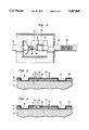
FIG. 1 is a perspective view of a semiconductor wafer that has been prepared to construct an electrode tip in accordance with the method of the present invention.
FIG. 2 is a closer view of the island of FIG. 1 on which the electrode tip is to be formed.
FIG. 3 is a cross sectional view of the island of FIG. 1.
FIG. 4 is a view of the island of FIG. 3 after etching of the electrode tip.
DETAILED DESCRIPTION OF THE PREFERRED EMBODIMENT
The method of the invention is best described with respect to the semiconductor wafer 10 shown in FIGS. 1 through 4. The semiconductor wafer 10 includes a p-doped silicon substrate 15 which serves as a base and has its surfaces normal to the <100> crystal face. An n-doped epitaxial layer 20 is grown on the surface of the p-doped substrate 15. The epitaxial layer 20 in the preferred embodiment is approximately 20 micrometers thick.
Using standard photolithographic techniques, the epitaxial layer 20 is etched through to the substrate 15 to form an island 25. Although only one island is shown, an island is formed for each electrode tip that is to be fabricated on the semiconductor wafer 10. Each island of epitaxy 25 is isolated by an isolation region 30 which has been etched through to the substrate 15.
The epitaxial layer 20 is also etched through to the substrate 15 to form a substrate connection region 35. Other areas of the epitaxial layer 20 may also be structured by the etching. These structured portions of the epitaxial layer may provide a bonding site where the wafer 10 is joined with, for example, a cover plate having a corresponding tunnel sensor electrode.
A patterned insulating layer 40 is applied over the exposed surfaces of the semiconductor wafer 10. The insulating layer 40 may be formed as a layer of silicon nitride, silicon oxide, or both. The insulating layer is masked using photolithography techniques and etched leaving exposed first and second regions 45, 50 on the island 25. First and second regions 45, 50 are thus not covered by the insulating layer 40. Additionally, the substrate connection region 35 is not covered by the insulating layer.
Metallization is applied to the semiconductor wafer 10 after the patterned insulating layer 40 has been etched to form the first and second exposed regions 45 and 50. The metallization is patterned to form at least two conductive paths. The conductive paths are preferably made from gold and are structured using standard pattern forming techniques.
The first conductive path includes a first bus bar 55 which is common to all of the islands. The first bus bar 55 is connected to a first bus supply pad 60. A metal branch strip 65 extends from the first bus bar 55 to each island 25. A substantially square metallization pad 70 is connected to two oppositely extending metal support strips 75, 80. One metal support strip 75 connects the metallization pad 70 to the branch strip 65. The other metal support strip 80 connects the metallization pad 70 to an anchor pad 85. The metallization pad 70 is in electrical contact with the epitaxial layer 20 in the first exposed region 45 of the island 25.
The second conductive path includes a second bus bar 90 which is also common to all of the islands. The second bus bar is connected to a second bus supply pad 95. A second metal branch strip 100 extends from the second bus bar 90 to each island 25 through a resistor 105. A second metallization pad 110 is connected to the branch strip 100 and is placed in electrical contact with the epitaxial layer 20 in the second exposed region 50 of the island 25. The second metallization pad 110 is preferably formed to cover substantially all of the second exposed region 50 thereby limiting any undercutting of the epitaxial layer 20 beneath the region 50 when the wafer 10 is exposed to the etchant.
A metal substrate connection 115 is applied to the substrate 15 in the substrate connection region 35. This allows application of a voltage potential to the substrate 15.
Certain electrochemical etchants, such as KOH, have etch rates which are dependent on the electrical potential of the semiconductor. For example, and without limitation, a positive electrical potential applied to silicon in the presence of a KOH etchant results in a decrease in the etching rate by a factor of several hundred. This etchant property is advantageously utilized in the method of the present invention.
The semiconductor wafer 10 is subject to a KOH etchant or the like. While subject to the etchant, the first conductive path and the substrate connection pad are held at a first voltage potential. In the embodiment described herein, the first potential is the same potential as the KOH etchant. The bus bar 90 of the second conductive path is connected to a second voltage potential at which the etch rate of the etchant is inhibited. This second voltage potential is thus supplied to the island 25 through the resistor 105. In the embodiment described herein, the second potential is positive with respect to the KOH etchant.
The island 25 is initially held at the first potential because it is connected to the first conductive path by the substantially square metallization pad 70. Since the first region 45 connected to the metallization pad 70 is not protected while it is at the first voltage potential, the first region 45 is undercut until it forms an electrode tip 120 as shown in FIG. 4. The etchant continues to undercut the first region 45 until the electrode tip is no longer in contact with the metallization pad 70.
Once the electrode tip 120 is no longer in contact with the metallization pad 70, the island 25 is effectively disconnected from the first conductive path and the first voltage potential. Since the island 25 is then effectively connected only to the second conductive path at the second metallization pad 110, the effect of the resistor becomes negligible and the potential of the island 25 approaches the second voltage potential. This inhibits further etching of the electrode tip 120 or that particular island while allowing the remaining electrode tips on the other islands to be completed. Thus, the wafer 10 need not be removed from the etchant as each electrode tip is successively completed. Rather, the potential of each island will automatically approach the second voltage potential as the respective electrode tip is completed and will thus be protected.
In the embodiment described herein, the n-doped island, after completion of etching, is at a positive potential with respect to the p-doped substrate, so that the junction between the island and the substrate forms a back-biased diode.
While several embodiments of the invention have been described hereinabove, those of ordinary skill in the art will recognize that the embodiments may be modified and altered without departing from the central spirit and scope of the invention. Thus, the preferred embodiments described hereinabove are to be considered in all respects as illustrative and not restrictive, the scope of the invention being indicated by the appended claims rather than by the foregoing description. Therefore, it is the intention of the inventor to embrace herein all changes which come within the meaning and range of equivalency of the claims.