US5406283A - Multi-bit oversampled DAC with dynamic element matching - Google Patents
Multi-bit oversampled DAC with dynamic element matching Download PDFInfo
- Publication number
- US5406283A US5406283A US08/055,713 US5571393A US5406283A US 5406283 A US5406283 A US 5406283A US 5571393 A US5571393 A US 5571393A US 5406283 A US5406283 A US 5406283A
- Authority
- US
- United States
- Prior art keywords
- output
- digital
- converter
- input
- signal
- Prior art date
- Legal status (The legal status is an assumption and is not a legal conclusion. Google has not performed a legal analysis and makes no representation as to the accuracy of the status listed.)
- Expired - Fee Related
Links
- 230000004044 response Effects 0.000 claims abstract description 9
- 238000012935 Averaging Methods 0.000 claims description 44
- 239000003990 capacitor Substances 0.000 claims description 23
- 238000006243 chemical reaction Methods 0.000 description 18
- 238000000034 method Methods 0.000 description 16
- 238000012546 transfer Methods 0.000 description 12
- 238000013459 approach Methods 0.000 description 10
- 230000000875 corresponding effect Effects 0.000 description 10
- 238000010586 diagram Methods 0.000 description 6
- 230000009471 action Effects 0.000 description 5
- 238000012937 correction Methods 0.000 description 5
- 230000000737 periodic effect Effects 0.000 description 5
- 230000001419 dependent effect Effects 0.000 description 4
- 235000009508 confectionery Nutrition 0.000 description 3
- 230000000694 effects Effects 0.000 description 3
- 230000006870 function Effects 0.000 description 3
- 238000001228 spectrum Methods 0.000 description 3
- 230000006399 behavior Effects 0.000 description 2
- 230000006872 improvement Effects 0.000 description 2
- 238000002347 injection Methods 0.000 description 2
- 239000007924 injection Substances 0.000 description 2
- 230000007246 mechanism Effects 0.000 description 2
- 238000013139 quantization Methods 0.000 description 2
- 238000005070 sampling Methods 0.000 description 2
- 238000004088 simulation Methods 0.000 description 2
- 230000001629 suppression Effects 0.000 description 2
- 230000009897 systematic effect Effects 0.000 description 2
- 238000009966 trimming Methods 0.000 description 2
- 101150108015 STR6 gene Proteins 0.000 description 1
- 101100386054 Saccharomyces cerevisiae (strain ATCC 204508 / S288c) CYS3 gene Proteins 0.000 description 1
- 230000002596 correlated effect Effects 0.000 description 1
- 238000005516 engineering process Methods 0.000 description 1
- 238000003384 imaging method Methods 0.000 description 1
- 238000004519 manufacturing process Methods 0.000 description 1
- 239000011159 matrix material Substances 0.000 description 1
- 239000002184 metal Substances 0.000 description 1
- 238000005192 partition Methods 0.000 description 1
- 230000002265 prevention Effects 0.000 description 1
- 230000000135 prohibitive effect Effects 0.000 description 1
- 238000007493 shaping process Methods 0.000 description 1
- 101150035983 str1 gene Proteins 0.000 description 1
- 238000012360 testing method Methods 0.000 description 1
Images


Classifications
-
- H—ELECTRICITY
- H03—ELECTRONIC CIRCUITRY
- H03M—CODING; DECODING; CODE CONVERSION IN GENERAL
- H03M1/00—Analogue/digital conversion; Digital/analogue conversion
- H03M1/06—Continuously compensating for, or preventing, undesired influence of physical parameters
- H03M1/0617—Continuously compensating for, or preventing, undesired influence of physical parameters characterised by the use of methods or means not specific to a particular type of detrimental influence
- H03M1/0634—Continuously compensating for, or preventing, undesired influence of physical parameters characterised by the use of methods or means not specific to a particular type of detrimental influence by averaging out the errors, e.g. using sliding scale
- H03M1/0656—Continuously compensating for, or preventing, undesired influence of physical parameters characterised by the use of methods or means not specific to a particular type of detrimental influence by averaging out the errors, e.g. using sliding scale in the time domain, e.g. using intended jitter as a dither signal
- H03M1/066—Continuously compensating for, or preventing, undesired influence of physical parameters characterised by the use of methods or means not specific to a particular type of detrimental influence by averaging out the errors, e.g. using sliding scale in the time domain, e.g. using intended jitter as a dither signal by continuously permuting the elements used, i.e. dynamic element matching
- H03M1/0665—Continuously compensating for, or preventing, undesired influence of physical parameters characterised by the use of methods or means not specific to a particular type of detrimental influence by averaging out the errors, e.g. using sliding scale in the time domain, e.g. using intended jitter as a dither signal by continuously permuting the elements used, i.e. dynamic element matching using data dependent selection of the elements, e.g. data weighted averaging
-
- H—ELECTRICITY
- H03—ELECTRONIC CIRCUITRY
- H03M—CODING; DECODING; CODE CONVERSION IN GENERAL
- H03M1/00—Analogue/digital conversion; Digital/analogue conversion
- H03M1/66—Digital/analogue converters
- H03M1/74—Simultaneous conversion
- H03M1/80—Simultaneous conversion using weighted impedances
- H03M1/802—Simultaneous conversion using weighted impedances using capacitors, e.g. neuron-mos transistors, charge coupled devices
- H03M1/804—Simultaneous conversion using weighted impedances using capacitors, e.g. neuron-mos transistors, charge coupled devices with charge redistribution
- H03M1/806—Simultaneous conversion using weighted impedances using capacitors, e.g. neuron-mos transistors, charge coupled devices with charge redistribution with equally weighted capacitors which are switched by unary decoded digital signals
-
- H—ELECTRICITY
- H03—ELECTRONIC CIRCUITRY
- H03M—CODING; DECODING; CODE CONVERSION IN GENERAL
- H03M3/00—Conversion of analogue values to or from differential modulation
- H03M3/30—Delta-sigma modulation
- H03M3/458—Analogue/digital converters using delta-sigma modulation as an intermediate step
- H03M3/464—Details of the digital/analogue conversion in the feedback path
-
- H—ELECTRICITY
- H03—ELECTRONIC CIRCUITRY
- H03M—CODING; DECODING; CODE CONVERSION IN GENERAL
- H03M3/00—Conversion of analogue values to or from differential modulation
- H03M3/30—Delta-sigma modulation
- H03M3/50—Digital/analogue converters using delta-sigma modulation as an intermediate step
- H03M3/502—Details of the final digital/analogue conversion following the digital delta-sigma modulation
Definitions
- the present invention relates in general to oversampling converters, and more particularly to a multi-bit (D/A) digital-to-analogue converter with dynamic element matching.
- D/A multi-bit
- Oversampling methods are known in the art of A/D and D/A conversion for overcoming problems associated with the use of analogue low-pass filters in conventional pulse code modulation. More particularly, in conventional systems, low-pass filters must be used to limit aliasing noise in A/D conversion and to smooth the output analogue signal in D/A conversion.
- VLSI does not lend itself well to the fabrication of high-precision analogue circuits.
- a novel class of dynamic element matching techniques is applied to multi-bit Sigma-Delta converters for translating the harmonic distortion components of the non-ideal feedback D/A converter to high frequency components which can then be filtered out by use of a decimation filter.
- a novel feedback D/A converter is provided for use within a Sigma-Delta A/D converter in which individual level averaging is provided for converting distortion components caused by element mismatch in the feedback D/A converter to high frequency noise lying outside of the passband.
- This noise which is due to element mismatch, has a similar frequency behaviour as quantization noise. Consequently, the accuracy requirements on the feedback D/A converter of the present invention are reduced without increasing the baseband noise appreciably.
- pipelining and periodic capacitor averaging techniques are used for translating the harmonic distortion components of the non-ideal D/A converter in an oversampled Sigma-Delta D/A converter to frequency components in the vicinity of f s/ 2, where f s is the sampling frequency. These frequency components can then be filtered out utilizing an analog lowpass anti-imaging filter.
- the tones generated utilizing pipelining with capacitor averaging are significantly further from the passband.
- FIG. 1 is a simplified block diagram of a multi-bit Sigma-Delta A/D converter according to the prior art
- FIG. 2a shows for the A/D converter of FIG. 1, the transfer characteristics of a two bit, three level ideal feedback D/A converter (i), and the transfer characteristics where there is a mismatch between unit elements in the feedback D/A converter (ii) and (iii);
- FIG. 2b shows the output V f (n) of the feedback D/A converter of FIG. 1 with V in (n) equal 0.25 for (i) an ideal D/A converter, (ii) a non-ideal D/A converter, (iii) a D/A converter with clocked averaging, and (iv) a D/A converter with individual averaging;
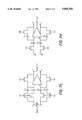
- FIG. 3 is a block diagram of an internal D/A converter incorporating individual level averaging
- FIG. 4 is a schematic representation of a three-bit clocked flipping scheme for the D/A converter of FIG. 3;
- FIG. 5 appears out of routine order following FIG. 3, and shows a block diagram of a second order three-bit D/A converter applying individual level averaging according to the present invention
- FIG. 6 is a schematic diagram of a switched capacitor array for implementing the three-bit D/A converter of FIGS. 3 and 5;
- FIG. 7(a) to (d) show a switching scheme and circuit for implementing a multiply-by-two circuit with capacitor averaging according to an alternative embodiment of the invention.
- FIG. 1 shows a typical, simplified block diagram of a multi-bit Sigma-Delta A/D converter according to the prior art, comprising a summer 1 for receiving an input analog signal V in (n).
- An output of summer 1 is connected to the input of a loop filter 3 having a transfer function H(z).
- An output of loop filter 3 is connected to the input of an N-bit A/D converter 5.
- the output signal V out (n) from A/D converter 5 is fed back via N-bit D/A converter 7 to the negative input of summer 1.
- the D/A converter 7 will have three levels corresponding to: “0”, “1.1/2.3” and “1” (i.e. transfer characteristic ⁇ 1) as shown in FIG. 2a (ii). If unit element flipping is done at a clock frequency f clk , then at every clock cycle, the transfer characteristic ⁇ 2 of D/A converter 7 will be shown in FIG. 2a(iii), whose levels are “0", "1.2/2.3” and "1". If for example a dc input V in (n) of "0.25" is applied to V in (n) of the first order ⁇ - ⁇ modulator of FIG.
- V f (n) For the normal non-ideal feedback D/A converter 7, the feedback signal V f (n) will no longer be periodic.
- the initial value of the integrator in the first order coder i.e. loop filter 3
- the ⁇ - ⁇ coder output is "00", “01", “00", “01” for the first four cycles. Therefore V f (n) will consist of "0”, “1.1/2.3”, “0", "1.1/2.3” as shown in FIG. 2b(ii). It is seen that even though the feedback signal V f (n) is interpolating between the input signal of "0.25", the average value of V f (n) is less than "0.25" and a conversion error is created. This conversion error is fed back to the input of the ⁇ - ⁇ coder, and stored in the integrator.
- the conventional clocked averaging approach endeavors to correct this conversion error by averaging the E DAC (Error of the internal D/A converter 7).
- E DAC Error of the internal D/A converter 7
- the averaging mechanism provided by the feedback loop of the ⁇ - ⁇ converter can interact with the averaging mechanism provided by the clocked averaging approach.
- V out (2) "01" and the curve ⁇ 2 of FIG. 2a(iii) is activated, giving V f (2) a value of "1.1/2.3".
- V out (3) is "00" , resulting in a V f (3) of "0”.
- V f (n) differs from 0.25, and like the case discussed above in which there is no unit element flipping, a conversion error is introduced.
- the conversion error stored in the integrator is negative. Again, when the absolute value of this conversion error is larger than 1 LSB of the forward A/D converter 5, an extra "00" will be generated.
- cancellation at any D/A level depends on the relative timing between the interpolating waveform V f (n) at the feedback node and the flipping waveform for selecting between the two unit elements characterized by transfer functions ⁇ 1 and ⁇ 2.
- the interpolating waveform V f (n) is a pulse density modulated representation of the instantaneous value of the input. Therefore, given an input sine wave at a particular frequency, the interpolating waveform can interact with the flipping operation in such a way that a different amount of cancellation is achieved for different D/A levels.
- the low frequency portion of the resulting signal which is obtained by time averaging the output of D/A converter 7, will then be distorted from the original sine wave. Furthermore the resulting distortion, which is dependent on the amount of cancellation, is related to the flipping frequency. This distortion can generate tones that are functions of the input frequency and flipping frequency, as discussed in B. Leung, "Architectures for Multi-bit Oversampled DAC Employing Dynamic Element Matching Techniques," 1991 IEEE International Symposium on Circuits and Systems, pp. 1657-1660 (May, 1991).
- the individual level averaging system cycles through all unit elements used to represent an individual digital code.
- V out (n) for the first four cycles is again assumed to be "00", “01", “00", “01”
- the D/A converter 7 output V f (n) is shown in FIG. 2b(iv).
- V out (1) "00"
- the curve ⁇ 1 is selected, and V f (1) will be "0".
- the fact that the ⁇ 1 curve has been used for the code "00" is now returned in memory, as discussed in greater detail below with reference to FIG. 3.
- V out (2) "01" and the curve ⁇ 1 is selected, which means that V f (2) will be "1.1/2.3". Again the fact that the ⁇ 1 curve has been used for the code "01" is stored in memory.
- the averaging activity applied to the D/A converter 7 does not interfere with the averaging activity provided by the negative feedback action of the ⁇ - ⁇ coder. This in turn ensures that cancellation of the error E DAC can be achieved regardless of the interpolation waveform.
- a D/A converter for implementing the individual level averaging approach of the present invention.
- a digital input signal L is applied to a thermometer-type encoder 9 and to a memory implemented by pointers and update circuits 11, which can be implemented as a set of registers.
- the enboder 9 sets high the number of output lines M thereof equal to the digital code L.
- the decoded signal M and an M-bit pointer signal from circuits 11 are applied to MxM switch 13 which in response selects predetermined ones of M unit elements 15.
- the outputs of unit elements 15 are applied to an output analog summer 17.
- a memory is introduced for each transfer curve of the D/A converter at each level.
- the input code is 01 and a different memory location corresponding to the level 01 provides the pointer for selecting the appropriate D/A converter transfer curve.
- the D/A converter output will be 1.1/2.3, which is different from the clocked averaging case when the curve ⁇ 2 is selected and a value of 1.2/2.3 is generated.
- the memory corresponding to the level 01 is now updated and points to the curve ⁇ 2 .
- the input code is 00. Since at T clk the memory corresponding to 00 was updated, the curve ⁇ 2 is selected this time and a 0 is generated. Finally, at 4T clk the input code is 01.
- the unit elements 15 are flipped with respect to one another for reducing distortion in the output signal for a sinusoidal input.
- An example of the proposed flipping scheme for the A/D converter of FIG. 3 having three bits (i.e. eight unit elements 15) is shown in FIG. 4.
- In 0 . . . In 7 represent eight unit elements of the D/A converter that have a slight mismatch among them.
- Out 0 . . . Out 7 is a linear array of unit elements which generate the final analog value corresponding to a given input digital code.
- the clocked flipping algorithm works by flipping the transfer characteristics of the D/A converter as follows: First of all, the top n/2 elements are swapped with the bottom n/2 elements at a rate of f clk .
- n/4 elements are swapped with the next n/4 elements at the rate of f clk /2.
- the bottom two partitions of n/4 elements are swapped among themselves.
- adjacent pairs of elements are swapped at the rate of f clk /4 .
- the flipping algorithm is implemented in the present invention by the D/A converter shown in FIG. 3, and the frequency spectrum of the output indicates that the harmonic distortions have been modulated to frequencies around multiples of f clk /8, instead of to white noise.
- a comparison to the random averaging case indicates that this approach can increase the SNR performance by 15 dB for a 0.1% systematic linear gradient mismatch between the elements in the 3-bit D/A converter.
- the cancellation cycle for a D/A converter with N elements is dependent on the digital input.
- a 2-bit D/A converter which as four elements with values: 1.1, 1.2, 1.3, 1.4.
- For an input code of 01 four D/A output signals 1.1/5, 1.2/5, 1.3/5, 1.4/5 have to be generated to ensure that the average analog output is exactly 1/4, which means that the cancellation cycle is 4.
- FIG. 5 shows the topology of a three-bit second-order multi-loop ⁇ - ⁇ D/A converter.
- the digital input i.e. PCM code
- the digital input is subtracted in summer 18 by the three-bit fed-back code, and the difference is applied to a digital integrator 19.
- the output of the first integrator 19 is subtracted from the three-bit fed-back code in a further summer 21, and the summer 21 output is applied to a second integrator 23.
- the output of the second integrator 23 is truncated with the digital quantizer 25 to obtain the three-bit output code.
- the three-bit pulse-density modulated code from the quantizer 25 is fed into a three-bit internal D/A converter of the form depicted in FIG. 3.
- a second order MASH D/A converter with a 3-bit internal D/A converter can also be implemented.
- a fully differential switched capacitor array may be used to implement the three-bit internal D/A converter of the present invention.
- the simplified circuit diagram of the D/A converter according to the preferred embodiment is shown in FIG. 6.
- the MSB b 2 is used to select the reference voltages, V r+ and V r- for the differential structure, while the bits S 0 , S 1 , S 2 and S 3 are encoded according to the truth table in Table 2 (i.e. via the pointers and update circuits 11 of FIG. 3).
- the eight unit elements are implemented differentially with four unit elements 29-35 connected to the inverting input of a differential amplifier 36 and unit elements 37-43 connected to the noninverting input of differential amplifier 36.
- the unit elements and the+and--outputs of differential amplifier 36 are clocked via non-overlapping clocks cl 2 and cl 1 .
- the lower voltage rail is enabled for applying Vr- and Vr+ to the left and right capacitor charging gates, respectively, for the top row of unit elements 29-35, and Vr+ and Vr- are applied to the left and right charging gates, respectively, of the lower row of unit elements 37-43.
- a predetermined pair 29,37 or 31,39 or 35,43 will be selected for applying differential charge to the amplifier 36.
- all elements used to represent an individual digital code are exercised sequentially so that error due to element mismatch has a high frequency spectrum, instead of a white spectrum as, as exhibited by conventional random averaging.
- the three-bit ⁇ - ⁇ DAC has been implemented with a 1.2 ⁇ m CMOB double-poly/double-metal technology, using both single-ended and differential designs. Test results were obtained with the single-ended version. The chip was tested at a clock rate of 200 KHz with an 800 Hz input signal. When different dynamio element matching techniques were applied, considerable harmonic distortion suppression was obtained. For the individual level averaging technique, a 24 dB improvement of harmonic distortion suppression was achieved.
- the SNRs (signal-to-noise ratios) of both multi-loop and MASH structures for conventional random averaging and individual level averaging techniques with an equivalent capacitor mismatch of 1% are shown in Table 3.
- An internal D/A for implementing pipelined capacitor averaging can be realized using switched capacitor implementation so that the overall linearity is limited by non-ideal effects of the subblocks from each stage, as discussed in F. Wang, G. Temes, S. Law, "A Quasi-Passive CMOS Pipeline D/A Converter," IEEE Journal of Solid-State Circuits, pp. 1752-1755 (December, 1989). These non idealities stem from errors due to non-ideal opamps, switches and capacitors. Unlike a pipelined A/D converter, a pipelined D/A converter, does not need a sample and hold circuit and there is no S/H error.
- the D/A subconverter error due to capacitor mismatch can be eliminated if only 1 bit is resolved per stage.
- N-bit D/A converter this means the number of stages equals N and the multiply circuits become multiply-by-two circuits.
- N for the internal D/A converter is small, typically on the order of three to four. Consequently the increase in hardware is not prohibitive for this application.
- the offset error is eliminated if a 1-bit D/A converter is used with fully differential architecture, the offset error is eliminated.
- the differential charge injection can be eliminated by employing a correlated double sampling technique, as discussed in B. Song, M. Tompsett, et al., "A 12-bit 1-Msample/s Capacitor Error-Averaging Pipelined A/D Converter," IEEE Journal of Solid-State Circuits, pp. 1324-1333 (December, 1988).
- the proposed scheme modulates the harmonic distortion components to f s /2-f harmonic . It should be noted that if this technique is applied to a Nyquist rate pipelined D/A converter, the modulated harmonic distortion components will fall into the passband and generate undesirable tones.
- the averaging action increases the baseband noise because the high frequency quantization noise is being modulated into the passband.
- For a multiply-by-two circuit only 2 unit capacitors are involved. Consequently only two elements need to be averaged and the harmonic distortion components will always be modulated to frequencies around f/2, as opposed to frequencies around f s /M, as in the conventional clocked averaging approach. From simulations the proposed invention enjoys a 10 db improvement over the random averaging approach in dynamic range for a third order oversampled D/A converter with a 3-bit pipelined internal D/A converter having a 0.1% random mismatch.
Abstract
A Sigma-Delta converter, has a receiver for receiving an input digital signal; a digital loop filter and quantizer having an input and an output; a summer having a first input connected to the receiver, a second input connected to the output of the digital loop filter and quantizer, and an output connected to the input of the digital loop filter and quantizer for subtracting from the input digital signal an output digital signal from the digital loop filter and quantizer, and in response generating a difference signal for application to the input of the digital loop filter and quantizer; and a digital-to-analog converter having a plurality of unit elements with minor mismatching therebetween, for receiving and converting to analog the output digital signal from the digital loop filter and quantizer, and in response generating an output analog signal, wherein the digital-to-analog converter has a selector for cyclically selecting successive different permutations of the unit elements for converting each value of the output digital signal thereby cancelling the mismatching between unit elements.
Description
The present invention relates in general to oversampling converters, and more particularly to a multi-bit (D/A) digital-to-analogue converter with dynamic element matching.
Oversampling methods are known in the art of A/D and D/A conversion for overcoming problems associated with the use of analogue low-pass filters in conventional pulse code modulation. More particularly, in conventional systems, low-pass filters must be used to limit aliasing noise in A/D conversion and to smooth the output analogue signal in D/A conversion. However, VLSI does not lend itself well to the fabrication of high-precision analogue circuits.
Recent advances in oversampling techniques are discussed in a paper entitled Oversampling Methods for A/D and D/A Conversion by James C. Candy and Gabor C. Temes. Candy and Temes discuss a number of embodiments of Sigma-Delta modulators for oversampling conversion. One problem discussed by Candy and Temes is the provision of a feedback D/A converter in multi-bit Sigma-Delta converters. Specifically, the conversion error in the feedback D/A converter must be very small (i.e. less than half the least significant bit of the final output digital word). This is because any D/A conversion error which is added to the D/A output signal is directly subtracted from the input signal to the Sigma-Delta converter so as to appear in the digital output of the converter. Candy and Temes discuss a number of strategies for overcoming the problem of D/A error in Delta-Sigma modulators, such as trimming of D/A converter elements, randomization of errors introduced by mismatching of components, and digital correction of the D/A conversion error.
However, the prior art approach of trimming components has been found to be extremely expensive, and the use of digital error correction results in a requirement for extra correction hardware, as described in R. H. Walden, Catultepe, G. C. Temes, "Architectures for high-order multibit Σ-Δ modulators," Proceedings of the 1990 IEEE International Symposium On Circuits and Systems, pp. 895-898 (May, 1990). The use of random averaging is known to result in a reduced signal-to-noise ratio (SNR) because all the harmonic distortions have been translated into white noise that falls partly inside the passband, as described in R. Carley, "A Noise-Shaping Coder Topology for 15+ Bit Converters," IEEE Journal of Solid-State Circuits, pp. 267-273 (April, 1989). Straightforward application of clocked averaging results in tones falling inside the passband, as well as an increase in passband noise, as discussed in greater detail below and as discussed in Yashui Sakina, P. Gray, "Multi-bit Σ-Δ analog to digital converters with nonlinearity correction using dynamic barrel shifting," Master Thesis, pp. 24-32 (June 1990) & B. Leung, "Architectures for Multi-bit Oversampling A/D Converter Employing Dynamic Element Matching Techniques," 1991 IEEE International Symposium on Circuits and Systems, pp. 1657-1660 (May, 1991).
According to the present invention, a novel class of dynamic element matching techniques is applied to multi-bit Sigma-Delta converters for translating the harmonic distortion components of the non-ideal feedback D/A converter to high frequency components which can then be filtered out by use of a decimation filter.
More particularly, a novel feedback D/A converter is provided for use within a Sigma-Delta A/D converter in which individual level averaging is provided for converting distortion components caused by element mismatch in the feedback D/A converter to high frequency noise lying outside of the passband. This noise, which is due to element mismatch, has a similar frequency behaviour as quantization noise. Consequently, the accuracy requirements on the feedback D/A converter of the present invention are reduced without increasing the baseband noise appreciably.
According to a second dynamic element matching technique of the present invention, pipelining and periodic capacitor averaging techniques are used for translating the harmonic distortion components of the non-ideal D/A converter in an oversampled Sigma-Delta D/A converter to frequency components in the vicinity of f s/ 2, where fs is the sampling frequency. These frequency components can then be filtered out utilizing an analog lowpass anti-imaging filter. Compared to conventional clocked averaging schemes as discussed below, the tones generated utilizing pipelining with capacitor averaging are significantly further from the passband.
A detailed description of prior art conventional clocked averaging systems and the system of the present invention are provided herein below with reference to the following drawings, in which:
FIG. 1 is a simplified block diagram of a multi-bit Sigma-Delta A/D converter according to the prior art;
FIG. 2a shows for the A/D converter of FIG. 1, the transfer characteristics of a two bit, three level ideal feedback D/A converter (i), and the transfer characteristics where there is a mismatch between unit elements in the feedback D/A converter (ii) and (iii);
FIG. 2b shows the output Vf (n) of the feedback D/A converter of FIG. 1 with Vin (n) equal 0.25 for (i) an ideal D/A converter, (ii) a non-ideal D/A converter, (iii) a D/A converter with clocked averaging, and (iv) a D/A converter with individual averaging;
FIG. 3 is a block diagram of an internal D/A converter incorporating individual level averaging;
FIG. 4 is a schematic representation of a three-bit clocked flipping scheme for the D/A converter of FIG. 3;
FIG. 5 appears out of routine order following FIG. 3, and shows a block diagram of a second order three-bit D/A converter applying individual level averaging according to the present invention;
FIG. 6 is a schematic diagram of a switched capacitor array for implementing the three-bit D/A converter of FIGS. 3 and 5; and
FIG. 7(a) to (d) show a switching scheme and circuit for implementing a multiply-by-two circuit with capacitor averaging according to an alternative embodiment of the invention.
One of the main considerations for incorporating a multi-bit over a single-bit quantizer inside the feedback loop of a Sigma-Delta converter is the prevention of overloading and thus the provision of stability. This allows the use of higher order coders which can provide a much higher SNR for the same oversampling ratio. In addition, each extra bit in the quantizer provides a 6dB increase in the SNR.
FIG. 1 shows a typical, simplified block diagram of a multi-bit Sigma-Delta A/D converter according to the prior art, comprising a summer 1 for receiving an input analog signal Vin (n). An output of summer 1 is connected to the input of a loop filter 3 having a transfer function H(z). An output of loop filter 3 is connected to the input of an N-bit A/D converter 5. The output signal Vout (n) from A/D converter 5 is fed back via N-bit D/A converter 7 to the negative input of summer 1.
As an example, in the first order Sigma-Delta converter of FIG. 1 the D/A converter 7 may be considered as having two unit elements, for generating three analog output levels Vf (n)="0", "1/2" and "1" as shown in FIG. 2a(i).
If there is a mismatch between the two elements such that their values are "1.1" and "1.2", the D/A converter 7 will have three levels corresponding to: "0", "1.1/2.3" and "1" (i.e. transfer characteristic φ1) as shown in FIG. 2a (ii). If unit element flipping is done at a clock frequency fclk, then at every clock cycle, the transfer characteristic φ2 of D/A converter 7 will be shown in FIG. 2a(iii), whose levels are "0", "1.2/2.3" and "1". If for example a dc input Vin (n) of "0.25" is applied to Vin (n) of the first order Σ-Δ modulator of FIG. 1 with an ideal feedback D/A converter 7, the output Vout (n) will consist of a periodic digital sequence "00", "01", "00", "01" . . . etc, resulting in a periodic D/A output sequence Vf (n)="0", "1/2", "0", "1/2" as shown in FIG. 2b(i). This sequence will produce an average of "0.25", which is identical to the input.
For the normal non-ideal feedback D/A converter 7, the feedback signal Vf (n) will no longer be periodic. To analyze the behavior of the circuit consider the first four cycles. If the initial value of the integrator in the first order coder (i.e. loop filter 3) is assumed to be zero, then the Σ-Δ coder output is "00", "01", "00", "01" for the first four cycles. Therefore Vf (n) will consist of "0", "1.1/2.3", "0", "1.1/2.3" as shown in FIG. 2b(ii). It is seen that even though the feedback signal Vf (n) is interpolating between the input signal of "0.25", the average value of Vf (n) is less than "0.25" and a conversion error is created. This conversion error is fed back to the input of the Σ-Δ coder, and stored in the integrator.
In the situation considered above, a positive conversion error will be stored in the integrator and when the absolute value of the accumulated error is larger than 1 LSB of the forward A/D converter 5 an extra "0.1" will be generated. As a matter of fact, since the average value of the feedback signal Vf (n) is forced to be the same as the input Vin (n) value due to the negative feedback action of D/A converter 7, the value "1.1/2.3" will be generated more than 50% of the time to compensate for the error. This results in the output code changing from a periodic sequence of "00", "01", "00", "01" to one consisting of an extra "01" at predetermined intervals.
The conventional clocked averaging approach endeavors to correct this conversion error by averaging the EDAC (Error of the internal D/A converter 7). However, it has been found that the averaging mechanism provided by the feedback loop of the Σ-Δ converter can interact with the averaging mechanism provided by the clocked averaging approach. The feedback sequence Vf (n) for the clocked averaging algorithm is shown in FIG. 2b(iii). Again if it is assumed that Vout (n), and hence the input to D/A converter 7, is "00", "01", "00", "01" for the first four cycles, then Vout (1)="00" and the φ1 curve of FIG. 2a(ii) is activated. Therefore Vf (1)="0". Next, Vout (2)="01" and the curve φ2 of FIG. 2a(iii) is activated, giving Vf (2) a value of "1.1/2.3". At n=3 the curve 6, φ3 is activated. However due to the interpolating nature of the Σ-Δ modulator, the modulator output Vout (n) does not stay constant. Instead, Vout (3) is "00" , resulting in a Vf (3) of "0". Finally, at n=4 the curve φ2 is activated again. Again Vout (n) has been changed and Vout (4)="01", resulting in a D/A output Vf (4) of "1.2/2.3". It will be noted that this is identical to Vf (2) and therefore no cancellation has been achieved. Consequently the average value of Vf (n) differs from 0.25, and like the case discussed above in which there is no unit element flipping, a conversion error is introduced. However, in the present case, the conversion error stored in the integrator is negative. Again, when the absolute value of this conversion error is larger than 1 LSB of the forward A/D converter 5, an extra "00" will be generated.
It can be seen that cancellation at any D/A level depends on the relative timing between the interpolating waveform Vf (n) at the feedback node and the flipping waveform for selecting between the two unit elements characterized by transfer functions φ1 and φ2. In the case when the input is a sine wave instead of a dc signal, the interpolating waveform Vf (n) is a pulse density modulated representation of the instantaneous value of the input. Therefore, given an input sine wave at a particular frequency, the interpolating waveform can interact with the flipping operation in such a way that a different amount of cancellation is achieved for different D/A levels. The low frequency portion of the resulting signal, which is obtained by time averaging the output of D/A converter 7, will then be distorted from the original sine wave. Furthermore the resulting distortion, which is dependent on the amount of cancellation, is related to the flipping frequency. This distortion can generate tones that are functions of the input frequency and flipping frequency, as discussed in B. Leung, "Architectures for Multi-bit Oversampled DAC Employing Dynamic Element Matching Techniques," 1991 IEEE International Symposium on Circuits and Systems, pp. 1657-1660 (May, 1991).
To ensure that the averaging action occurs regardless of the nature of the interpolating waveform, the individual level averaging system according to the present invention cycles through all unit elements used to represent an individual digital code. With reference to the first order modulator of FIG. 1, where Vout (n) for the first four cycles is again assumed to be "00", "01", "00", "01", the D/A converter 7 output Vf (n) is shown in FIG. 2b(iv). At n=1, Vout (1)="00" and the curve φ1 is selected, and Vf (1) will be "0". The fact that the φ1 curve has been used for the code "00" is now returned in memory, as discussed in greater detail below with reference to FIG. 3. At n=2, Vout (2)="01" and the curve φ1 is selected, which means that Vf (2) will be "1.1/2.3". Again the fact that the φ1 curve has been used for the code "01" is stored in memory. At n=3, Vout (3)="00". Since at n=1 the curve φ1 has been used, this time the φ2 curve is selected. With Vout (3)="00" and aφ2 curve, Vf (3)="0". Finally at n=4, Vout (4) is "01". Again, since at n=2 the curve φ1 has been used, so this time the φ2 curve is selected and Vf (4)="1.2/2.3". Therefore, both the values "1.1/2.3" and "1.2/2.3" have been utilized to represent the digital code "01", giving an average value of "1/2". Consequently, the average value of Vf (n) is "0.25". This is identical to the input value and no conversion error is generated.
The output sequences Vf (n) for the different cases are now summarized in Table I.
                                  TABLE I
__________________________________________________________________________
DAC output V.sub.ρ (n) For Different Averaging Algorithms
V.sub.in = 0.25, First Order Σ-Δ Coder, 2 Unit Elements
                                Avg
Case          n = 1
                  n = 2
                       n = 3
                           n = 4
                                Value
                                    Error
__________________________________________________________________________
Ideal         0   0.5  0   0.5  0.25
                                    0
No Averaging  0
                   ##STR1##
                       0
                            ##STR2##
                                0.239
                                    -- 0.01 1
Clocked Averaging
              0
                   ##STR3##
                       0
                            ##STR4##
                                0.261
                                    0.01 1
Individual Level Averaging
              0
                   ##STR5##
                       0
                            ##STR6##
                                0.25
                                    0
__________________________________________________________________________
Thus, according to the present invention, the averaging activity applied to the D/A converter 7 does not interfere with the averaging activity provided by the negative feedback action of the Σ-Δ coder. This in turn ensures that cancellation of the error EDAC can be achieved regardless of the interpolation waveform.
According to the embodiment of FIG. 3, a D/A converter is provided for implementing the individual level averaging approach of the present invention. A digital input signal L is applied to a thermometer-type encoder 9 and to a memory implemented by pointers and update circuits 11, which can be implemented as a set of registers. The enboder 9 sets high the number of output lines M thereof equal to the digital code L. The decoded signal M and an M-bit pointer signal from circuits 11 are applied to MxM switch 13 which in response selects predetermined ones of M unit elements 15. The outputs of unit elements 15 are applied to an output analog summer 17. Thus, according to the D/A converter of FIG. 3, a memory is introduced for each transfer curve of the D/A converter at each level. This will ensure that all transfer curves corresponding to each digital code are exercised in the representation of that particular digital code. If this approach is applied to the first order coder example outlined above, the output of the first four cycles will again be 00, 01, 00, 01. At Tclk, the input code is 00 and the memory corresponding to the level 00 will provide the pointer that selects the appropriate D/A converter transfer curve. The algorithm begins with the curve φ1 (FIG. 2a(ii)) which means that the D/A converter output will be 0. The memory 11 corresponding to input code 00 is then updated and points to curve φ2. At 2Tclk, the input code is 01 and a different memory location corresponding to the level 01 provides the pointer for selecting the appropriate D/A converter transfer curve. Again starting off with curve φ1 the D/A converter output will be 1.1/2.3, which is different from the clocked averaging case when the curve φ2 is selected and a value of 1.2/2.3 is generated. The memory corresponding to the level 01 is now updated and points to the curve φ2. At 3Tclk, the input code is 00. Since at Tclk the memory corresponding to 00 was updated, the curve φ2 is selected this time and a 0 is generated. Finally, at 4Tclk the input code is 01. Again, since at 2Tclk the memory 11 was updated, the curve φ2 is selected. Hence the D/A converter has an output value of 1.2/2.3. Therefore both the values 1.1/2.3 and 1.2/2.3 have been utilized to represent the logic high portion of digital code L.
Thus, for a given code, the memory 11 selects a pointer to the switch matrix 13 which in turn provides the next set of unit elements 15. The pointer is then updated. Finally, the M=2n elements are activated and summed to form the analogue output.
As discussed above, the unit elements 15 are flipped with respect to one another for reducing distortion in the output signal for a sinusoidal input. An example of the proposed flipping scheme for the A/D converter of FIG. 3 having three bits (i.e. eight unit elements 15) is shown in FIG. 4. Here In0 . . . In7 represent eight unit elements of the D/A converter that have a slight mismatch among them. Out0 . . . Out7 is a linear array of unit elements which generate the final analog value corresponding to a given input digital code. The clocked flipping algorithm works by flipping the transfer characteristics of the D/A converter as follows: First of all, the top n/2 elements are swapped with the bottom n/2 elements at a rate of fclk. Secondly, the top n/4 elements are swapped with the next n/4 elements at the rate of fclk /2. At the same time the bottom two partitions of n/4 elements are swapped among themselves. Finally, adjacent pairs of elements are swapped at the rate of fclk /4 .
The flipping algorithm is implemented in the present invention by the D/A converter shown in FIG. 3, and the frequency spectrum of the output indicates that the harmonic distortions have been modulated to frequencies around multiples of fclk /8, instead of to white noise. A comparison to the random averaging case indicates that this approach can increase the SNR performance by 15 dB for a 0.1% systematic linear gradient mismatch between the elements in the 3-bit D/A converter.
For the above approach residual noise is still generated in the baseband due to incomplete cancellation. In order to get complete cancellation for a given digital input of D/A converter 7 (FIG. 3), a complete set of analog outputs corresponding to the digital input has to be selected. In the 2-bit case considered above, for the digital code 01, the set has two elements: 1.1/2.3 and 1.2/2.3. The number of elements in this set is referred to as the "cancellation cycle". As shown in Table 1, if the input Vin is 0.25 the output of D/A converter 7 is 0, 1.1/2.3, 0, 1.2/2.3 for the first four cycles. If Vin changes its value at, for example, cycle four, then D/A converter 7 has not exercised all of the analog outputs corresponding to the digital code 01 and errors will be generated. Consequently, to reduce the error due to imperfect the cancellation the cycle shoud be kept small. However, the cancellation cycle for a D/A converter with N elements is dependent on the digital input. As an example, consider a 2-bit D/A converter which as four elements with values: 1.1, 1.2, 1.3, 1.4. For an input code of 01, four D/A output signals 1.1/5, 1.2/5, 1.3/5, 1.4/5 have to be generated to ensure that the average analog output is exactly 1/4, which means that the cancellation cycle is 4. On the other hand, with an input code of 10, there are again four possible D/A output signals. 1.1+1.2/5, 1.2+1.3/5, 1.3+1.4/5, 1.4+1.1/5. In this case, only a sequence of two D/A outputs needs to be selected, namely 1.1+1.2/5 and 1.3+1.4/5 or 1.2+1.3/5 and 1.4+1.1/5, to ensure that the average analog output is 1/2. Therefore, the cancellation cycle in this case is only two. Since the cancellation cycle is input dependent, the algorithm which performs the D/A output selections for a given digital code should do so with the minimum cancellation cycle. Compared to the case when a fixed cancellation cycle is applied for all the input codes, this input dependent selection scheme results in a smaller "average" cancellation cycle. Simulations have confirmed that this technique can improve the signal to noise ratio of a third order Σ-Δ converter by up to 7 dB with an oversampling ratio of 32 and a 3-bit internal, having a systematic linear gradient mismatch of 0.1%.
FIG. 5 shows the topology of a three-bit second-order multi-loop Σ-Δ D/A converter. The digital input, (i.e. PCM code) is subtracted in summer 18 by the three-bit fed-back code, and the difference is applied to a digital integrator 19. The output of the first integrator 19 is subtracted from the three-bit fed-back code in a further summer 21, and the summer 21 output is applied to a second integrator 23. The output of the second integrator 23 is truncated with the digital quantizer 25 to obtain the three-bit output code. The three-bit pulse-density modulated code from the quantizer 25 is fed into a three-bit internal D/A converter of the form depicted in FIG. 3. A second order MASH D/A converter with a 3-bit internal D/A converter can also be implemented.
A fully differential switched capacitor array may be used to implement the three-bit internal D/A converter of the present invention. The simplified circuit diagram of the D/A converter according to the preferred embodiment is shown in FIG. 6. The thermometer code 5; is generated from the two LSB's, b1 and b0 of L=b2, b1, b0. The MSB b2 is used to select the reference voltages, Vr+ and Vr- for the differential structure, while the bits S0, S1, S2 and S3 are encoded according to the truth table in Table 2 (i.e. via the pointers and update circuits 11 of FIG. 3).
              TABLE 2
______________________________________
Occurence  b.sub.1
                 b.sub.0   s.sub.0
                               s.sub.1
                                      s.sub.2
                                          s.sub.3
______________________________________
Always     0     0         0   0      0   0
1st        0     1         1   0      0   0
2nd        0     1         0   1      0   0
3rd        0     1         0   0      1   0
4th        0     1         0   0      0   1
1st        1     0         1   1      0   0
2nd        1     0         0   1      1   0
3rd        1     0         0   0      1   1
4th        1     0         1   0      0   1
1st        1     1         1   1      1   0
2nd        1     1         0   1      1   1
3rd        1     1         1   0      1   1
4th        1     1         1   1      0   1
______________________________________
The details of operation of the circuit shown in FIG. 6 would be well known to a person skilled in the art. Basically, the eight unit elements are implemented differentially with four unit elements 29-35 connected to the inverting input of a differential amplifier 36 and unit elements 37-43 connected to the noninverting input of differential amplifier 36. The unit elements and the+and--outputs of differential amplifier 36 are clocked via non-overlapping clocks cl2 and cl1. Thus, in the case of a three-bit digital code L=001, then b1 =0and b0 =1. According to the truth table illustrated in Table 2, one of the decoded gate control signals s0, s1, s2 and s3 will be at a logic high level. Since b2 =0, then the lower voltage rail is enabled for applying Vr- and Vr+ to the left and right capacitor charging gates, respectively, for the top row of unit elements 29-35, and Vr+ and Vr- are applied to the left and right charging gates, respectively, of the lower row of unit elements 37-43. Depending on the occurrence of the code b,b0 =01, b0, a predetermined pair 29,37 or 31,39 or 35,43 will be selected for applying differential charge to the amplifier 36. For example, if each unit element is considered to have a value of 1, then for the first occurrence of b,b0 =01 unit elements 29 and 37 will be charged to 1 and -1, respectively, while unit elements 31-35 are charged to -1 and unit elements 39-43 are charged to 1.
If the next digital input code is L=010, then a predetermined two pairs of the upper and lower unit elements will be charged to -1 and the remaining two pairs of elements will be charged to 1, depending on the occurrence of b1, b0 =1.0.
If on the next clock cycle, the digital input code returns to L=001, then, since this is the second occurrence of b,b0 =01, then s1 =1 , while s0, s2 and s3 are all 0 resulting in unit elements 31 and 39 charging to 1 and -1, respectively, while unit elements 29, 33 and 35 each charge to -1 and unit elements 37, 41 and 43 each charge to 1. In this way, by permuting the D/A converter unit elements on a per level basis, all elements used to represent an individual digital code are exercised sequentially so that error due to element mismatch has a high frequency spectrum, instead of a white spectrum as, as exhibited by conventional random averaging.
The three-bit Σ-Δ DAC has been implemented with a 1.2 μm CMOB double-poly/double-metal technology, using both single-ended and differential designs. Test results were obtained with the single-ended version. The chip was tested at a clock rate of 200 KHz with an 800 Hz input signal. When different dynamio element matching techniques were applied, considerable harmonic distortion suppression was obtained. For the individual level averaging technique, a 24 dB improvement of harmonic distortion suppression was achieved. The SNRs (signal-to-noise ratios) of both multi-loop and MASH structures for conventional random averaging and individual level averaging techniques with an equivalent capacitor mismatch of 1% are shown in Table 3.
              TABLE 3
______________________________________
Comparison of SNR for Different Architectures
       Random Averaging
                    Indiv. Level Averaging
______________________________________
Multi-Loop
         53dB           59dB
MASH     51dB           61dB
______________________________________
An internal D/A for implementing pipelined capacitor averaging can be realized using switched capacitor implementation so that the overall linearity is limited by non-ideal effects of the subblocks from each stage, as discussed in F. Wang, G. Temes, S. Law, "A Quasi-Passive CMOS Pipeline D/A Converter," IEEE Journal of Solid-State Circuits, pp. 1752-1755 (December, 1989). These non idealities stem from errors due to non-ideal opamps, switches and capacitors. Unlike a pipelined A/D converter, a pipelined D/A converter, does not need a sample and hold circuit and there is no S/H error. Because there is no A/D converter in a pipelined D/A converter extra circuitry for digital error correction is not needed, as discussed in Y. Lin, B. Kim, P. Gray, "A 13-b 2.5 MHz Self-Calibrated Pipelined A/D Converter in 3-um CMOS," IEEE Journal of Solid-State Circuits, pp. 628-636 (April 1991). The overall linearity is limited by the following errors of the individual stages:
1) D/A subconverter error related to capacitor mismatch.
2) Summing error related to finite opamp gain, charge feedthrough, injection, opamp offset.
3) Multiplying error related to finite opamp gain, capacitor mismatch.
The D/A subconverter error due to capacitor mismatch can be eliminated if only 1 bit is resolved per stage. For an N-bit D/A converter this means the number of stages equals N and the multiply circuits become multiply-by-two circuits. For an oversampled D/A converter even though the overall resolution is high, the resolution N for the internal D/A converter is small, typically on the order of three to four. Consequently the increase in hardware is not prohibitive for this application. Furthermore, if a 1-bit D/A converter is used with fully differential architecture, the offset error is eliminated.
All charge circuits based on opamps transfer charges between capacitors rather imperfectly because of finite amplifier gain. Finite opamp gain errors can be compensated for using circuit techniques like calibration, but the simplest way is to maintain a high DC gain, as discussed in K. Bult, G. Geelen, "A Fast-Settling CMOS Op AMP with 90 dB DC Gain and 116 MHz Unity-Gain Frequency," Digest if Technical Papers, International Solid-State Circuits Conference 1990, pp. 108-109 (February 1990). The opamp offset error is automatically cancelled because the signal is sampled on the input capacitors by connecting the opamp in a unity-gain configuration. The differential charge injection can be eliminated by employing a correlated double sampling technique, as discussed in B. Song, M. Tompsett, et al., "A 12-bit 1-Msample/s Capacitor Error-Averaging Pipelined A/D Converter," IEEE Journal of Solid-State Circuits, pp. 1324-1333 (December, 1988).
Considering the third error source which results from capacitor mismatch, in the past a technique has been applied to Nyquist rate pipelined converters that involves using an extra clock phase to average the error due to capacitor mismatch. For a D/A converter this scheme will result in extra delay and reduce the conversion speed. The present invention attempts to eliminate this delay by exploiting the fact that the digital input of the internal D/A converter for an oversampled D/A converter stays relatively constant during adjacent clock cycles. Consequently, instead of using an extra clock phase the present approach distributes the averaging action over two adjacent clock cycles as shown in FIGS. 7(a) to (d). The capacitors in FIG. 7 are assumed to have mismatches as follows: ##EQU1## where α1, α2 <<1.
The circuit of FIG. 7 forms a multiply-by-2 circuit with capacitor averaging such that in the firstclock phase (FIG. 7 (a)) φ1 (n), bN (n)Vref /2N is sampled, and Vout (n) is reset to 0. For φ2 (n+1), (FIG. 7(b)) from charge conversation Vout (n+1/2)×(2+α1 +α2)bN (n)Vref /2N. In the second clock phase (FIG. 7(c)) φ1 (n+1), bN (n+1) Vref /2N is sampled and Vout (n+1) reset to 0. For φ2 (n+1), (FIG. 7(d)), from charge conversion Vout (n+3/2)=(2-α1 -α2)bN (n+1)Vref /2N.
From the frequency domain point of view the proposed scheme modulates the harmonic distortion components to fs /2-fharmonic. It should be noted that if this technique is applied to a Nyquist rate pipelined D/A converter, the modulated harmonic distortion components will fall into the passband and generate undesirable tones. For the oversampled D/A converter, in addition to the modulation of harmonic distortion components the averaging action increases the baseband noise because the high frequency quantization noise is being modulated into the passband. For a multiply-by-two circuit only 2 unit capacitors are involved. Consequently only two elements need to be averaged and the harmonic distortion components will always be modulated to frequencies around f/2, as opposed to frequencies around fs /M, as in the conventional clocked averaging approach. From simulations the proposed invention enjoys a 10 db improvement over the random averaging approach in dynamic range for a third order oversampled D/A converter with a 3-bit pipelined internal D/A converter having a 0.1% random mismatch.
Other embodiments and variations of the invention are possible within the sphere and scope of the description herein.
Claims (4)
1. A Sigma-Delta converter, comprising:
a) means for receiving an input digital signal;
b) at least one digital loop filter and quantizer having an input and an output;
c) at least one subtractor having a first input connected to said means for receiving, a second input connected to said output of said at least one digital loop filter and quantizer, and an output connected to said input of said at least one digital loop filter and quantizer for subtracting from said input digital signal an output digital signal from said at least one digital loop filter and quantizer, and in response generating a difference signal for application to said input of said at least one digital loop filter and quantizer; and
d) a digital-to-analog converter having a plurality of unit elements with minor mismatching therebetween, for receiving and converting to analog said output digital signal from said at least one digital loop filter and quantizer, and in response generating an output analog signal, wherein said digital-to-analog converter comprises means for cyclically selecting successive different permutations of said unit elements for converting each value of said output digital signal thereby canceling said mismatching between unit elements.
2. The Sigma-Delta converter of claim 1, wherein said means for cyclically selecting further comprises:
e) means for receiving and encoding each said value of said output digital signal and in response generating an encoded digital signal;
f) means for receiving said output digital signal and in response generating and updating a pointer signal for each value of said output digital signal;
g) a crosspoint switch for receiving said pointer signal and in response transmitting said encoded digital signal to a predetermined one or more of said unit elements according to said successive different permutations; and
h) an analog summer for summing respective signals output from said unit elements and in response generating said analog output signal.
3. The Sigma-Delta converter of claim 2, wherein said plurality of unit elements further comprise a switched capacitor array and said analog summer further comprises a differential amplifier having inverting and non-inverting inputs connected to respective portions of said array.
4. The Sigma-Delta converter of claim 1, wherein said digital-to-analog converter comprises one or more series connected multiply-by-two circuits each incorporating capacitor averaging means.
Applications Claiming Priority (2)
| Application Number | Priority Date | Filing Date | Title |
|---|---|---|---|
| GB9209498 | 1992-05-01 | ||
| GB929209498A GB9209498D0 (en) | 1992-05-01 | 1992-05-01 | Multi-bit dac with dynamic element matching |
Publications (1)
| Publication Number | Publication Date |
|---|---|
| US5406283A true US5406283A (en) | 1995-04-11 |
Family
ID=10714895
Family Applications (1)
| Application Number | Title | Priority Date | Filing Date |
|---|---|---|---|
| US08/055,713 Expired - Fee Related US5406283A (en) | 1992-05-01 | 1993-04-29 | Multi-bit oversampled DAC with dynamic element matching |
Country Status (3)
| Country | Link |
|---|---|
| US (1) | US5406283A (en) |
| CA (1) | CA2095156A1 (en) |
| GB (1) | GB9209498D0 (en) |
Cited By (74)
| Publication number | Priority date | Publication date | Assignee | Title |
|---|---|---|---|---|
| US5608401A (en) * | 1994-12-28 | 1997-03-04 | Lucent Technologies Inc. | Three-level digital-to-analog converter for low-power consumption |
| US5760726A (en) * | 1996-08-23 | 1998-06-02 | Motorola, Inc. | Digital-to-analog converter with dynamic matching and bit splitting |
| WO1998048515A1 (en) * | 1997-04-18 | 1998-10-29 | Steensgaard Madsen Jesper | Oversampled digital-to-analog converter based on nonlinear separation and linear recombination |
| EP0927868A2 (en) * | 1997-12-22 | 1999-07-07 | Philips Patentverwaltung GmbH | Sensor device with measurement error recognition |
| US5936562A (en) * | 1997-06-06 | 1999-08-10 | Analog Devices, Inc. | High-speed sigma-delta ADCs |
| US5977899A (en) * | 1997-09-25 | 1999-11-02 | Analog Devices, Inc. | Digital-to-analog converter using noise-shaped segmentation |
| US5982313A (en) * | 1997-06-06 | 1999-11-09 | Analog Devices, Inc. | High speed sigma-delta analog-to-digital converter system |
| US5986595A (en) * | 1996-02-28 | 1999-11-16 | University College Cork | Reduction of mismatch errors for multibit oversampled data converters |
| US5995031A (en) * | 1997-07-09 | 1999-11-30 | Mitsubishi Denki Kabushiki Kaisha | D/A and A/D converters |
| WO2000039932A2 (en) * | 1998-12-14 | 2000-07-06 | Steensgaard Madsen Jesper | Serial d/a converter |
| US6107947A (en) * | 1996-11-05 | 2000-08-22 | University College Cork | Parallel sigma delta modulator |
| US6198417B1 (en) | 1998-01-29 | 2001-03-06 | Massachusetts Institute Of Technology | Pipelined oversampling A/D converter |
| US6232897B1 (en) * | 1999-07-12 | 2001-05-15 | National Instruments Corporation | System and method for calibrating an analog to digital converter through stimulation of current generators |
| US6289070B1 (en) | 1997-04-22 | 2001-09-11 | Silicon Laboratories, Inc. | Digital isolation system with ADC offset calibration including coarse offset |
| WO2001067614A1 (en) * | 2000-02-22 | 2001-09-13 | The Regents Of The University Of California | Digital cancellation of d/a converter noise in pipelined a/d converters |
| US6297755B2 (en) | 1997-04-22 | 2001-10-02 | Silicon Laboratories, Inc. | Analog isolation system with digital communication across a capacitive barrier |
| SG83798A1 (en) * | 1999-06-07 | 2001-10-16 | Nippon Precision Circuits | Delta sigma d/a converter |
| US6323796B1 (en) | 1997-04-22 | 2001-11-27 | Silicon Laboratories, Inc. | Digital isolation system with ADC offset calibration |
| US6330330B2 (en) | 1997-04-22 | 2001-12-11 | Silicon Laboratories, Inc. | External resistor and method to minimize power dissipation in DC holding circuitry for a communication system |
| US6348884B1 (en) * | 1999-01-06 | 2002-02-19 | Jesper Steensgaard-Madsen | Idle-tone-free mismatch-shaping encoders |
| US6359983B1 (en) | 1997-04-22 | 2002-03-19 | Silicon Laboratories, Inc. | Digital isolation system with data scrambling |
| WO2002027944A2 (en) * | 2000-09-29 | 2002-04-04 | Teradyne, Inc. | Digital to analog converter employing sigma-delta loop and feedback dac model |
| US6380874B1 (en) * | 1999-07-12 | 2002-04-30 | National Instruments Corporation | System and method for self-calibrating a multi-bit delta-sigma analog to digital converter using dynamic element matching |
| US6385235B1 (en) | 1997-04-22 | 2002-05-07 | Silicon Laboratories, Inc. | Direct digital access arrangement circuitry and method for connecting to phone lines |
| US6389061B1 (en) | 1997-04-22 | 2002-05-14 | Silicon Laboratories Inc. | Isolation system with digital communication across a capacitive barrier |
| US6389134B1 (en) * | 1997-04-22 | 2002-05-14 | Silicon Laboratories, Inc. | Call progress monitor circuitry and method for a communication system |
| US6408034B1 (en) | 1997-04-22 | 2002-06-18 | Silicon Laboratories, Inc. | Framed delta sigma data with unlikely delta sigma data patterns |
| US6426715B1 (en) * | 1999-10-27 | 2002-07-30 | Koninklijke Philips Electronics N.V. | Digital to analog converter |
| US6426714B1 (en) * | 2001-06-26 | 2002-07-30 | Nokia Corporation | Multi-level quantizer with current mode DEM switch matrices and separate DEM decision logic for a multibit sigma delta modulator |
| US6430229B1 (en) | 1997-04-22 | 2002-08-06 | Silicon Laboratories Inc. | Capacitive isolation system with digital communication and power transfer |
| US6442271B1 (en) | 1997-04-22 | 2002-08-27 | Silicon Laboratories, Inc. | Digital isolation system with low power mode |
| US6442213B1 (en) | 1997-04-22 | 2002-08-27 | Silicon Laboratories Inc. | Digital isolation system with hybrid circuit in ADC calibration loop |
| US6441759B1 (en) | 2000-08-30 | 2002-08-27 | Hrl Laboratories, Llc | Multi-bit ΔΣ modulator having linear output |
| US6445324B1 (en) * | 2000-10-06 | 2002-09-03 | Stmicroelectronics S.R.L. | Method for dynamic matching of the elements of an integrated multibit digital-to-analog converter with balanced output for audio applications |
| US6456712B1 (en) | 1997-04-22 | 2002-09-24 | Silicon Laboratories Inc. | Separation of ring detection functions across isolation barrier for minimum power |
| US6473011B1 (en) | 1999-08-19 | 2002-10-29 | Jesper Steensgaard-Madsen | Serial D/A converter compensating for capacitor mismatch errors |
| US6473019B1 (en) | 2001-06-21 | 2002-10-29 | Nokia Corporation | Low capacitance, low kickback noise input stage of a multi-level quantizer with dithering and multi-threshold generation for a multi-bit sigma-delta modulator |
| US6473017B1 (en) * | 2000-03-13 | 2002-10-29 | Research Foundation Of The City University Of New York | One-bit second order sigma-delta modulator including a polynomial vector quantizer |
| US6480602B1 (en) | 1997-04-22 | 2002-11-12 | Silicon Laboratories, Inc. | Ring-detect interface circuitry and method for a communication system |
| US6498825B1 (en) | 1997-04-22 | 2002-12-24 | Silicon Laboratories Inc. | Digital access arrangement circuitry and method for connecting to phone lines having a DC holding circuit with programmable current limiting |
| US6504864B1 (en) | 1997-04-22 | 2003-01-07 | Silicon Laboratories Inc. | Digital access arrangement circuitry and method for connecting to phone lines having a second order DC holding circuit |
| WO2003003583A2 (en) * | 2001-06-27 | 2003-01-09 | Nokia Corporation | Method and apparatus for suppressing tones induced by cyclic dynamic element matching (dem) algorithms |
| US6516024B1 (en) | 1997-04-22 | 2003-02-04 | Silicon Laboratories Inc. | Digital access arrangement circuitry and method for connecting to phone lines having a DC holding circuit with low distortion and current limiting |
| US6518905B2 (en) | 2000-12-21 | 2003-02-11 | Wright State University | Parallel time interleaved delta sigma modulator |
| US6522277B2 (en) | 2001-02-05 | 2003-02-18 | Asahi Kasei Microsystems, Inc. | Circuit, system and method for performing dynamic element matching using bi-directional rotation within a data converter |
| US6531973B2 (en) | 2000-09-11 | 2003-03-11 | Broadcom Corporation | Sigma-delta digital-to-analog converter |
| US6556161B2 (en) * | 2000-04-04 | 2003-04-29 | Koninklijke Philips Electronics N.V. | Digital to analog converter employing dynamic element matching |
| US6577257B2 (en) | 2000-09-11 | 2003-06-10 | Broadcom Corporation | Methods and systems for digital dither |
| US6577261B2 (en) | 2000-09-11 | 2003-06-10 | Broadcom Corporation | Method and apparatus for mismatched shaping of an oversampled converter |
| US6587560B1 (en) * | 1997-04-22 | 2003-07-01 | Silicon Laboratories Inc. | Low voltage circuits powered by the phone line |
| US20030137439A1 (en) * | 2002-01-24 | 2003-07-24 | Broadcom Corporation | Shuffler apparatus and related dynamic element matching technique for linearization of unit-element digital-to-analog converters |
| US6614377B1 (en) | 2002-02-08 | 2003-09-02 | Analog Devices, Inc. | Data-directed scrambler for noise-shaping mixed-signal converters with an arbitrary number of quantization levels |
| US20030218214A1 (en) * | 2002-05-22 | 2003-11-27 | Ryuta Tsuchiya | MIS semiconductor device and manufacturing method thereof |
| US6661362B2 (en) | 2000-09-11 | 2003-12-09 | Broadcom Corporation | Methods and systems for high speed quantizers |
| US20050036604A1 (en) * | 1997-04-22 | 2005-02-17 | Silicon Laboratories Inc. | Direct digital access arrangement circuitry and method for connecting DSL circuitry to phone lines |
| US20050110664A1 (en) * | 2003-11-26 | 2005-05-26 | Feng Chen | Suppressing digital-to-analog converter (DAC) error |
| US6919832B2 (en) | 2000-09-11 | 2005-07-19 | Broadcom Corporation | Methods and systems for high speed quantizers |
| US20060158360A1 (en) * | 2003-06-18 | 2006-07-20 | Koninklijke Philips Electronics N.V. | Digital to analog converter |
| US20070040720A1 (en) * | 2005-08-20 | 2007-02-22 | Samsung Electronics Co., Ltd. | Method of matching dynamic elements and multi-bit data converter |
| US20070057824A1 (en) * | 2005-08-23 | 2007-03-15 | Fujitsu Limited | Semiconductor integrated circuit having switch circuit of digital signal |
| US20070126615A1 (en) * | 2005-12-06 | 2007-06-07 | Yi Gyeong Kim | Multi-bit sigma-delta modulator and digital-to-analog converter with one digital-to-analog capacitor |
| US20080079615A1 (en) * | 2006-08-30 | 2008-04-03 | Sang-Ho Kim | Multi-Bit Data Converter Using Data Weight Averaging |
| US20080139126A1 (en) * | 2006-12-08 | 2008-06-12 | Sung-Jun Lee | Method for measuring variable bandwidth wireless channel and transmitter and receiver therefor |
| US20090140897A1 (en) * | 2007-11-30 | 2009-06-04 | John Healy | Gain matching method and system for single bit gain ranging analog-to-digital converter |
| US20090224953A1 (en) * | 2008-03-07 | 2009-09-10 | Qualcomm Incorporated | Apparatus and method for dynamic circuit element selection in a digital-to-analog converter |
| US20100103013A1 (en) * | 2008-10-23 | 2010-04-29 | Microchip Technology Incorporated | Method and Apparatus for Dithering in Multi-Bit Sigma-Delta Digital-to-Analog Converters |
| US20110012767A1 (en) * | 2009-07-16 | 2011-01-20 | Microchip Technology Incorporated | 2-Phase Gain Calibration And Scaling Scheme For Switched Capacitor Sigma-Delta Modulator |
| US20110163901A1 (en) * | 2009-07-16 | 2011-07-07 | Microchip Technology Incorporated | 2-phase gain calibration and scaling scheme for switched capacitor sigma-delta modulator using a chopper voltage reference |
| WO2014085161A1 (en) * | 2012-11-30 | 2014-06-05 | Analog Devices, Inc. | Enhanced second order noise shaped segmentation and dynamic element matching technique |
| US9337874B1 (en) * | 2014-12-18 | 2016-05-10 | Intel IP Corporation | High-speed digital signal processing systems |
| US9705521B1 (en) * | 2016-07-27 | 2017-07-11 | Silicon Laboratories Inc. | Noise shaping signed digital-to-analog converter |
| US10128859B1 (en) * | 2018-02-20 | 2018-11-13 | Analog Devices Global Unlimited Company | Correlated double sampling analog-to-digital converter |
| US10715160B1 (en) | 2019-09-13 | 2020-07-14 | Analog Devices International Unlimited Company | Low noise analog-to-digital converter |
| CN114050828A (en) * | 2022-01-07 | 2022-02-15 | 武汉杰开科技有限公司 | Digital-to-analog converter, mismatch calibration method of digital-to-analog converter and chip |
Families Citing this family (3)
| Publication number | Priority date | Publication date | Assignee | Title |
|---|---|---|---|---|
| EP0704978B1 (en) * | 1994-09-30 | 2003-06-18 | Kabushiki Kaisha Toshiba | Selection device for selecting electric cells and apparatus using the same |
| US6740387B1 (en) | 1998-06-09 | 2004-05-25 | 2752-3273 Quebec Inc. | Synthetic turf game surface |
| US6602113B2 (en) | 1999-12-08 | 2003-08-05 | 2752-3273 Quebec Inc. | Method for forming synthetic turf game surfaces |
Citations (5)
| Publication number | Priority date | Publication date | Assignee | Title |
|---|---|---|---|---|
| US4404544A (en) * | 1981-04-09 | 1983-09-13 | Bell Telephone Laboratories, Incorporated | μ-Law/A-law PCM CODEC |
| US4988900A (en) * | 1988-12-28 | 1991-01-29 | Sgs-Thomson Microelectronics S.A. | Analog signal waveform generator |
| US5072219A (en) * | 1989-02-07 | 1991-12-10 | Texas Instruments Incorporated | Digital-analog conversion system including a digital modulator having several quantification levels, associated with a digital-analog converter |
| US5225835A (en) * | 1991-03-29 | 1993-07-06 | Kabushiki Kaisha Toshiba | Sigma delta type digital/analog converter system |
| US5252973A (en) * | 1991-07-03 | 1993-10-12 | Sony Corporation | Apparatus for digital-to-analogue conversion |
-
1992
- 1992-05-01 GB GB929209498A patent/GB9209498D0/en active Pending
-
1993
- 1993-04-29 US US08/055,713 patent/US5406283A/en not_active Expired - Fee Related
- 1993-04-29 CA CA002095156A patent/CA2095156A1/en not_active Abandoned
Patent Citations (5)
| Publication number | Priority date | Publication date | Assignee | Title |
|---|---|---|---|---|
| US4404544A (en) * | 1981-04-09 | 1983-09-13 | Bell Telephone Laboratories, Incorporated | μ-Law/A-law PCM CODEC |
| US4988900A (en) * | 1988-12-28 | 1991-01-29 | Sgs-Thomson Microelectronics S.A. | Analog signal waveform generator |
| US5072219A (en) * | 1989-02-07 | 1991-12-10 | Texas Instruments Incorporated | Digital-analog conversion system including a digital modulator having several quantification levels, associated with a digital-analog converter |
| US5225835A (en) * | 1991-03-29 | 1993-07-06 | Kabushiki Kaisha Toshiba | Sigma delta type digital/analog converter system |
| US5252973A (en) * | 1991-07-03 | 1993-10-12 | Sony Corporation | Apparatus for digital-to-analogue conversion |
Non-Patent Citations (26)
| Title |
|---|
| B. Leung, "Architectures for Multi-Bit Oversampled A/D Converter Employing Dynamic Element Matching Techniques," 1991 IEEE International Symposium on Circuits and Systems, pp. 1657-1660 (May 1991). |
| B. Leung, "Pipelined Multi-bit Oversampled Digital to Analog Converters with Capacitor Averaging," Analog Integrated Circuits and Signal Processing, An International Journal, pp. 139-156 (vol. 2, No. 2, Apr., 1992). |
| B. Leung, Architectures for Multi Bit Oversampled A/D Converter Employing Dynamic Element Matching Techniques, 1991 IEEE International Symposium on Circuits and Systems, pp. 1657 1660 (May 1991). * |
| B. Leung, Pipelined Multi bit Oversampled Digital to Analog Converters with Capacitor Averaging, Analog Integrated Circuits and Signal Processing, An International Journal, pp. 139 156 (vol. 2, No. 2, Apr., 1992). * |
| B. Song, M. Tompsett, K. Lakshmikumar, "A 12-bit 1-Msample/s Capacitor Error-Averaging Pipelined A/D Converter," IEEE Journal of Solid-State Circuits, vol. 23, No. 6, pp. 1324-1333 (Dec., 1988). |
| B. Song, M. Tompsett, K. Lakshmikumar, A 12 bit 1 Msample/s Capacitor Error Averaging Pipelined A/D Converter, IEEE Journal of Solid State Circuits, vol. 23, No. 6, pp. 1324 1333 (Dec., 1988). * |
| F. Chen, B. Leung, "A Multi-Bit Σ-.increment. DAC with Dynamic Element Matching Techniques," Proceedings of IEEE Custom Integrated Circuit Conference, pp. 16.2.1-16.2.4 (May, 1992). |
| F. Chen, B. Leung, A Multi Bit DAC with Dynamic Element Matching Techniques, Proceedings of IEEE Custom Integrated Circuit Conference, pp. 16.2.1 16.2.4 (May, 1992). * |
| F. Wang, G. Temes, S. Law, "A Quasi-Passive CMOS Pipeline D/A Converter," IEEE Journal of Solid-State Circuits, vol. 24, No. 6, pp. 1752-1755 (Dec., 1989). |
| F. Wang, G. Temes, S. Law, A Quasi Passive CMOS Pipeline D/A Converter, IEEE Journal of Solid State Circuits, vol. 24, No. 6, pp. 1752 1755 (Dec., 1989). * |
| J. Fattaruso, Sami Kiriaki, Greg Warwar, Michiel de Wit, "Self-Calibration Techniques for a Second-Order Multi-bit Sigma-Delta Modulator," Digest of the 1993 IEEE International Solid-State Circuits Conference, pp. 228-229 (Feb., 1993). |
| J. Fattaruso, Sami Kiriaki, Greg Warwar, Michiel de Wit, Self Calibration Techniques for a Second Order Multi bit Sigma Delta Modulator, Digest of the 1993 IEEE International Solid State Circuits Conference, pp. 228 229 (Feb., 1993). * |
| K. Bult, G. Geelen, "A Fast-Settling CMOS Op AMP with 90dB DC Gain and 116 MHz Unity-Gain Frequency," Digest of Technical Papers, IEEE International Solid-State Circuits Conference 1990, pp. 108-109 (Feb., 1990). |
| K. Bult, G. Geelen, A Fast Settling CMOS Op AMP with 90dB DC Gain and 116 MHz Unity Gain Frequency, Digest of Technical Papers, IEEE International Solid State Circuits Conference 1990, pp. 108 109 (Feb., 1990). * |
| L. Richard Carley, "A Noise-Shaping Coder Topology For 15+ Bit Converters," IEEE Journal of Solid-State Circuits, vol. 24, No. 2, pp. 267-273 (Apr., 1989). |
| L. Richard Carley, "An Oversampling Analog-to-Digital Converter Topology for High Resolution Signal Acquisition Systems, " IEEE Transactions on Circuits and Systems, vol. CAS-34, No. 1, pp. 83-90 (Jan., 1987). |
| L. Richard Carley, A Noise Shaping Coder Topology For 15 Bit Converters, IEEE Journal of Solid State Circuits, vol. 24, No. 2, pp. 267 273 (Apr., 1989). * |
| L. Richard Carley, An Oversampling Analog to Digital Converter Topology for High Resolution Signal Acquisition Systems, IEEE Transactions on Circuits and Systems, vol. CAS 34, No. 1, pp. 83 90 (Jan., 1987). * |
| R. H. Walden, T, Cataltepe, G. C. Temes, "Architectures for High-Order Multibit Σ-.increment. Modulators," Proceeding of the 1990 IEEE International Symposium On Circuits and Systems, pp. 895-898 (May, 1990). |
| R. H. Walden, T, Cataltepe, G. C. Temes, Architectures for High Order Multibit Modulators, Proceeding of the 1990 IEEE International Symposium On Circuits and Systems, pp. 895 898 (May, 1990). * |
| T. Cataltepe, A. R. Kramer, L. E. Larson, G. C. Temes, R. H. Walden, "Digitally Corrected Multi-Bit Σ-.increment. Data Converters," Proceedings of the 1989 IEEE International Symposium On Circuits and Systems, pp. 647-650 (May, 1989). |
| T. Cataltepe, A. R. Kramer, L. E. Larson, G. C. Temes, R. H. Walden, Digitally Corrected Multi Bit Data Converters, Proceedings of the 1989 IEEE International Symposium On Circuits and Systems, pp. 647 650 (May, 1989). * |
| Y. Lin, B. Kim, P. Gray, "A 13-b 2.5-MHz Self-Calibrated Pipelined A/D Converter in 3-μm CMOS," IEEE Journal of Solid-State Circuits, vol. 26, No. 4, pp. 628-636 (Apr. 1991). |
| Y. Lin, B. Kim, P. Gray, A 13 b 2.5 MHz Self Calibrated Pipelined A/D Converter in 3 m CMOS, IEEE Journal of Solid State Circuits, vol. 26, No. 4, pp. 628 636 (Apr. 1991). * |
| Yasuaki Sakina, "Multi-Bit Σ.increment. Analog-to-Digital Converters with Nonlinearity Correction Using Dynamic Barrel Shifting," Master Thesis, pp. 1-76 (May, 1990). |
| Yasuaki Sakina, Multi Bit Analog to Digital Converters with Nonlinearity Correction Using Dynamic Barrel Shifting, Master Thesis, pp. 1 76 (May, 1990). * |
Cited By (174)
| Publication number | Priority date | Publication date | Assignee | Title |
|---|---|---|---|---|
| US5608401A (en) * | 1994-12-28 | 1997-03-04 | Lucent Technologies Inc. | Three-level digital-to-analog converter for low-power consumption |
| US5986595A (en) * | 1996-02-28 | 1999-11-16 | University College Cork | Reduction of mismatch errors for multibit oversampled data converters |
| US5760726A (en) * | 1996-08-23 | 1998-06-02 | Motorola, Inc. | Digital-to-analog converter with dynamic matching and bit splitting |
| US6107947A (en) * | 1996-11-05 | 2000-08-22 | University College Cork | Parallel sigma delta modulator |
| US5982317A (en) * | 1997-04-18 | 1999-11-09 | Jesper Steensgaard-Madsen | Oversampled digital-to-analog converter based on nonlinear separation and linear recombination |
| WO1998048515A1 (en) * | 1997-04-18 | 1998-10-29 | Steensgaard Madsen Jesper | Oversampled digital-to-analog converter based on nonlinear separation and linear recombination |
| US7301995B2 (en) | 1997-04-22 | 2007-11-27 | Silicon Laboratories Inc. | Direct digital access arrangement circuitry and method for connecting to phone lines |
| US6456712B1 (en) | 1997-04-22 | 2002-09-24 | Silicon Laboratories Inc. | Separation of ring detection functions across isolation barrier for minimum power |
| US7515672B2 (en) | 1997-04-22 | 2009-04-07 | Silicon Laboratories Inc. | Digital access arrangement circuitry and method for connecting to phone lines having a DC holding circuit with programmable current limiting |
| US7463675B2 (en) | 1997-04-22 | 2008-12-09 | Silicon Laboratories Inc. | Direct digital access arrangement circuitry and method for connecting to phone lines |
| US7362841B2 (en) | 1997-04-22 | 2008-04-22 | Silicon Laboratories Inc. | Digital access arrangement circuitry and method for connecting to phone lines having a DC holding circuit with switchable DC termination impedance |
| US7283584B2 (en) | 1997-04-22 | 2007-10-16 | Silicon Laboratories Inc. | Direct digital access arrangement circuitry and method for connecting to phone lines |
| US6289070B1 (en) | 1997-04-22 | 2001-09-11 | Silicon Laboratories, Inc. | Digital isolation system with ADC offset calibration including coarse offset |
| US7203224B2 (en) | 1997-04-22 | 2007-04-10 | Silicon Laboratories | Isolation system with digital communication across a capacitive barrier |
| US6297755B2 (en) | 1997-04-22 | 2001-10-02 | Silicon Laboratories, Inc. | Analog isolation system with digital communication across a capacitive barrier |
| US7200167B2 (en) | 1997-04-22 | 2007-04-03 | Silicon Laboratories Inc. | Direct digital access arrangement circuitry and method for connecting to phone lines |
| US7154940B2 (en) | 1997-04-22 | 2006-12-26 | Silicon Laboratories Inc. | Isolation system with digital communication across a capacitive barrier |
| US6330330B2 (en) | 1997-04-22 | 2001-12-11 | Silicon Laboratories, Inc. | External resistor and method to minimize power dissipation in DC holding circuitry for a communication system |
| US7072389B2 (en) | 1997-04-22 | 2006-07-04 | Silicon Laboratories Inc. | Direct digital access arrangement circuitry and method for connecting to phone lines |
| US6359983B1 (en) | 1997-04-22 | 2002-03-19 | Silicon Laboratories, Inc. | Digital isolation system with data scrambling |
| US7046755B2 (en) | 1997-04-22 | 2006-05-16 | Silicon Laboratories Inc. | Digital access arrangement circuitry and method for connecting to phone lines having a DC holding circuit with switchable time constants |
| US7003023B2 (en) | 1997-04-22 | 2006-02-21 | Silicon Laboratories Inc. | Digital isolation system with ADC offset calibration |
| US6385235B1 (en) | 1997-04-22 | 2002-05-07 | Silicon Laboratories, Inc. | Direct digital access arrangement circuitry and method for connecting to phone lines |
| US6389061B1 (en) | 1997-04-22 | 2002-05-14 | Silicon Laboratories Inc. | Isolation system with digital communication across a capacitive barrier |
| US6389134B1 (en) * | 1997-04-22 | 2002-05-14 | Silicon Laboratories, Inc. | Call progress monitor circuitry and method for a communication system |
| US6408034B1 (en) | 1997-04-22 | 2002-06-18 | Silicon Laboratories, Inc. | Framed delta sigma data with unlikely delta sigma data patterns |
| US6975723B2 (en) | 1997-04-22 | 2005-12-13 | Silicon Laboratories Inc. | Architecture for minimum loop current during ringing and caller ID |
| US6959083B2 (en) | 1997-04-22 | 2005-10-25 | Silicon Laboratories Inc. | Loop current monitor circuitry and method for a communication system |
| US6430229B1 (en) | 1997-04-22 | 2002-08-06 | Silicon Laboratories Inc. | Capacitive isolation system with digital communication and power transfer |
| US6442271B1 (en) | 1997-04-22 | 2002-08-27 | Silicon Laboratories, Inc. | Digital isolation system with low power mode |
| US6442213B1 (en) | 1997-04-22 | 2002-08-27 | Silicon Laboratories Inc. | Digital isolation system with hybrid circuit in ADC calibration loop |
| US6922469B2 (en) | 1997-04-22 | 2005-07-26 | Silicon Laboratories, Inc. | Separation of ring detection functions across isolation barrier for minimum power |
| US20050100104A1 (en) * | 1997-04-22 | 2005-05-12 | Silicon Laboratories Inc. | Digital access arrangement circuitry and method for connecting to phone lines having a DC holding circuit with programmable current limiting |
| US6587560B1 (en) * | 1997-04-22 | 2003-07-01 | Silicon Laboratories Inc. | Low voltage circuits powered by the phone line |
| US20020150151A1 (en) * | 1997-04-22 | 2002-10-17 | Silicon Laboratories Inc. | Digital isolation system with hybrid circuit in ADC calibration loop |
| US20020154702A1 (en) * | 1997-04-22 | 2002-10-24 | Silicon Laboratories Inc. | Direct digital access arrangement circuitry and method for connecting to phone lines |
| US20050036604A1 (en) * | 1997-04-22 | 2005-02-17 | Silicon Laboratories Inc. | Direct digital access arrangement circuitry and method for connecting DSL circuitry to phone lines |
| US20040228475A1 (en) * | 1997-04-22 | 2004-11-18 | Silicon Laboratories Inc. | External resistor and method to minimize power dissipation in DC holding circuitry for a communication system |
| US20040081232A1 (en) * | 1997-04-22 | 2004-04-29 | Silicon Laboratories Inc. | Isolation system with digital communication across a capacitive barrier |
| US6480602B1 (en) | 1997-04-22 | 2002-11-12 | Silicon Laboratories, Inc. | Ring-detect interface circuitry and method for a communication system |
| US6498825B1 (en) | 1997-04-22 | 2002-12-24 | Silicon Laboratories Inc. | Digital access arrangement circuitry and method for connecting to phone lines having a DC holding circuit with programmable current limiting |
| US20030002571A1 (en) * | 1997-04-22 | 2003-01-02 | Silicon Laboratories Inc. | Direct digital access arrangement circuitry and method for connecting to phone lines |
| US6323796B1 (en) | 1997-04-22 | 2001-11-27 | Silicon Laboratories, Inc. | Digital isolation system with ADC offset calibration |
| US20040161024A1 (en) * | 1997-04-22 | 2004-08-19 | Silicon Laboratories, Inc. | Direct digital access arrangement circuitry and method for connecting to phone lines |
| US6504864B1 (en) | 1997-04-22 | 2003-01-07 | Silicon Laboratories Inc. | Digital access arrangement circuitry and method for connecting to phone lines having a second order DC holding circuit |
| US6754341B2 (en) | 1997-04-22 | 2004-06-22 | Silicon Laboratories, Inc. | External resistor and method to minimize power dissipation in DC holding circuitry for a communication system |
| US6516024B1 (en) | 1997-04-22 | 2003-02-04 | Silicon Laboratories Inc. | Digital access arrangement circuitry and method for connecting to phone lines having a DC holding circuit with low distortion and current limiting |
| US20040101132A1 (en) * | 1997-04-22 | 2004-05-27 | Silicon Laboratories Inc. | Analog isolation system with digital communication across a capacitive barrier |
| US20040091100A1 (en) * | 1997-04-22 | 2004-05-13 | Silicon Laboratories Inc. | Loop current monitor circuitry and method for a communication system |
| US20040057524A1 (en) * | 1997-04-22 | 2004-03-25 | Silicon Laboratories Inc. | Digital isolation system with ADC offset calibration |
| US6683548B2 (en) | 1997-04-22 | 2004-01-27 | Silicon Laboratories Inc. | Analog isolation system with digital communication across a capacitive barrier |
| US6654409B1 (en) | 1997-04-22 | 2003-11-25 | Silicon Laboratories, Inc. | Direct digital access arrangement circuitry and method for connecting DSL circuitry to phone lines |
| US20030206626A1 (en) * | 1997-04-22 | 2003-11-06 | Scott Jeffrey W. | Low voltage circuits powered by the phone line |
| US20030194083A1 (en) * | 1997-04-22 | 2003-10-16 | Scott Jeffrey W. | Separation of ring detection functions across isolation barrier for minimum power |
| US20030091140A1 (en) * | 1997-04-22 | 2003-05-15 | Silicon Laboratories Inc. | Digital access arrangment circuitry and method for connecting to phone lines having a DC holding circuit with switchable DC termination impedance |
| US6570513B2 (en) | 1997-04-22 | 2003-05-27 | Silicon Laboratories Inc. | Isolation system with digital communication across a capacitive barrier |
| US6611553B1 (en) | 1997-04-22 | 2003-08-26 | Silicon Laboratories Inc. | Isolation system with digital communication across a capacitive barrier |
| US20040190670A1 (en) * | 1997-04-22 | 2004-09-30 | Silicon Laboratories Inc. | Digital access arrangement circuitry and method for connecting to phone lines having a DC holding circuit with switchable time constants |
| US5936562A (en) * | 1997-06-06 | 1999-08-10 | Analog Devices, Inc. | High-speed sigma-delta ADCs |
| US5982313A (en) * | 1997-06-06 | 1999-11-09 | Analog Devices, Inc. | High speed sigma-delta analog-to-digital converter system |
| US5995031A (en) * | 1997-07-09 | 1999-11-30 | Mitsubishi Denki Kabushiki Kaisha | D/A and A/D converters |
| US5977899A (en) * | 1997-09-25 | 1999-11-02 | Analog Devices, Inc. | Digital-to-analog converter using noise-shaped segmentation |
| EP0927868A2 (en) * | 1997-12-22 | 1999-07-07 | Philips Patentverwaltung GmbH | Sensor device with measurement error recognition |
| EP0927868A3 (en) * | 1997-12-22 | 2001-03-21 | Philips Patentverwaltung GmbH | Sensor device with measurement error recognition |
| US6198417B1 (en) | 1998-01-29 | 2001-03-06 | Massachusetts Institute Of Technology | Pipelined oversampling A/D converter |
| WO2000039932A3 (en) * | 1998-12-14 | 2001-02-22 | Steensgaard Madsen Jesper | Serial d/a converter |
| WO2000039932A2 (en) * | 1998-12-14 | 2000-07-06 | Steensgaard Madsen Jesper | Serial d/a converter |
| US6348884B1 (en) * | 1999-01-06 | 2002-02-19 | Jesper Steensgaard-Madsen | Idle-tone-free mismatch-shaping encoders |
| SG83798A1 (en) * | 1999-06-07 | 2001-10-16 | Nippon Precision Circuits | Delta sigma d/a converter |
| US6380874B1 (en) * | 1999-07-12 | 2002-04-30 | National Instruments Corporation | System and method for self-calibrating a multi-bit delta-sigma analog to digital converter using dynamic element matching |
| US6232897B1 (en) * | 1999-07-12 | 2001-05-15 | National Instruments Corporation | System and method for calibrating an analog to digital converter through stimulation of current generators |
| US6473011B1 (en) | 1999-08-19 | 2002-10-29 | Jesper Steensgaard-Madsen | Serial D/A converter compensating for capacitor mismatch errors |
| US6426715B1 (en) * | 1999-10-27 | 2002-07-30 | Koninklijke Philips Electronics N.V. | Digital to analog converter |
| WO2001067614A1 (en) * | 2000-02-22 | 2001-09-13 | The Regents Of The University Of California | Digital cancellation of d/a converter noise in pipelined a/d converters |
| US7006028B2 (en) | 2000-02-22 | 2006-02-28 | The Regents Of The University Of California | Digital background cancellation of digital to analog converter mismatch noise in analog to digital converters |
| US20050156773A1 (en) * | 2000-02-22 | 2005-07-21 | Ian Galton | Digital background cancellation of digital to analog converter mismatch noise in analog to digital converters |
| US6734818B2 (en) | 2000-02-22 | 2004-05-11 | The Regents Of The University Of California | Digital cancellation of D/A converter noise in pipelined A/D converters |
| US6473017B1 (en) * | 2000-03-13 | 2002-10-29 | Research Foundation Of The City University Of New York | One-bit second order sigma-delta modulator including a polynomial vector quantizer |
| US6556161B2 (en) * | 2000-04-04 | 2003-04-29 | Koninklijke Philips Electronics N.V. | Digital to analog converter employing dynamic element matching |
| US6441759B1 (en) | 2000-08-30 | 2002-08-27 | Hrl Laboratories, Llc | Multi-bit ΔΣ modulator having linear output |
| US20040252042A1 (en) * | 2000-09-11 | 2004-12-16 | Brooks Todd L. | Computer program product for mismatched shaping of an oversampled converter |
| US6531973B2 (en) | 2000-09-11 | 2003-03-11 | Broadcom Corporation | Sigma-delta digital-to-analog converter |
| US6577261B2 (en) | 2000-09-11 | 2003-06-10 | Broadcom Corporation | Method and apparatus for mismatched shaping of an oversampled converter |
| US6577257B2 (en) | 2000-09-11 | 2003-06-10 | Broadcom Corporation | Methods and systems for digital dither |
| US6771199B2 (en) | 2000-09-11 | 2004-08-03 | Broadcom Corporation | Method and apparatus for mismatched shaping of an oversampled converter |
| US6774830B2 (en) | 2000-09-11 | 2004-08-10 | Broadcom Corporation | Methods and systems for digital dither |
| US6628218B2 (en) * | 2000-09-11 | 2003-09-30 | Broadcom Corporation | Method and apparatus for mismatched shaping of an oversampled converter |
| US6661362B2 (en) | 2000-09-11 | 2003-12-09 | Broadcom Corporation | Methods and systems for high speed quantizers |
| US7002497B2 (en) | 2000-09-11 | 2006-02-21 | Broadcom Corporation | Methods and systems for digital dither |
| US20040021596A1 (en) * | 2000-09-11 | 2004-02-05 | Broadcom Corporation | Method and apparatus for mismatched shaping of an oversampled converter |
| US6950049B2 (en) | 2000-09-11 | 2005-09-27 | Broadcom Corporation | Computer program product for performing digital-to-analog conversion |
| US6940434B2 (en) | 2000-09-11 | 2005-09-06 | Broadcom Corporation | Methods and systems for digital dither |
| US20040233084A1 (en) * | 2000-09-11 | 2004-11-25 | Brooks Todd Lee | Methods and systems for digital dither |
| US7212142B2 (en) | 2000-09-11 | 2007-05-01 | Broadcom Corporation | Methods and systems for high speed quantizers |
| US6930626B2 (en) | 2000-09-11 | 2005-08-16 | Broadcom Corporation | Computer program product for mismatched shaping of an oversampled converter |
| US6816097B2 (en) | 2000-09-11 | 2004-11-09 | Broadcom Corporation | System and method for performing digital-to-analog conversion using a sigma-delta modulator |
| US20050040979A1 (en) * | 2000-09-11 | 2005-02-24 | Broadcom Corporation | Computer program product for performing digital-to-analog conversion |
| US6919832B2 (en) | 2000-09-11 | 2005-07-19 | Broadcom Corporation | Methods and systems for high speed quantizers |
| US20050128111A1 (en) * | 2000-09-11 | 2005-06-16 | Broadcom Corporation | Methods and systems for digital dither |
| WO2002027944A3 (en) * | 2000-09-29 | 2003-08-14 | Teradyne Inc | Digital to analog converter employing sigma-delta loop and feedback dac model |
| KR100829024B1 (en) | 2000-09-29 | 2008-05-14 | 테라다인 인코퍼레이티드 | Digital to analog converter employing sigma-delta loop and feedback dac model |
| WO2002027944A2 (en) * | 2000-09-29 | 2002-04-04 | Teradyne, Inc. | Digital to analog converter employing sigma-delta loop and feedback dac model |
| US6445324B1 (en) * | 2000-10-06 | 2002-09-03 | Stmicroelectronics S.R.L. | Method for dynamic matching of the elements of an integrated multibit digital-to-analog converter with balanced output for audio applications |
| US6518905B2 (en) | 2000-12-21 | 2003-02-11 | Wright State University | Parallel time interleaved delta sigma modulator |
| US6522277B2 (en) | 2001-02-05 | 2003-02-18 | Asahi Kasei Microsystems, Inc. | Circuit, system and method for performing dynamic element matching using bi-directional rotation within a data converter |
| WO2003001675A3 (en) * | 2001-06-21 | 2004-09-10 | Nokia Corp | Nmulti-level quantizer with dithering and multi-threshold generation for a multi-bt sigma-delta modulator |
| WO2003001675A2 (en) * | 2001-06-21 | 2003-01-03 | Nokia Corporation | Nmulti-level quantizer with dithering and multi-threshold generation for a multi-bt sigma-delta modulator |
| US6473019B1 (en) | 2001-06-21 | 2002-10-29 | Nokia Corporation | Low capacitance, low kickback noise input stage of a multi-level quantizer with dithering and multi-threshold generation for a multi-bit sigma-delta modulator |
| WO2003001674A3 (en) * | 2001-06-26 | 2003-04-10 | Nokia Corp | Multi-level quantizer delta sigma modulator with current mode dem and dem decision logic |
| EP1400017A2 (en) * | 2001-06-26 | 2004-03-24 | Nokia Corporation | A multi-level quantizer with current mode dem switch matrices and separate dem decision logic for a multibit sigma delta modulator |
| US6426714B1 (en) * | 2001-06-26 | 2002-07-30 | Nokia Corporation | Multi-level quantizer with current mode DEM switch matrices and separate DEM decision logic for a multibit sigma delta modulator |
| WO2003001674A2 (en) * | 2001-06-26 | 2003-01-03 | Nokia Corporation | Multi-level quantizer delta sigma modulator with current mode dem and dem decision logic |
| CN1327618C (en) * | 2001-06-26 | 2007-07-18 | 诺基亚有限公司 | Multi-level quantizer with current mode. DEM switch matrices and separate DEM decision logic for multibit sigma delta modulator |
| EP1400017A4 (en) * | 2001-06-26 | 2005-03-09 | Nokia Corp | A multi-level quantizer with current mode dem switch matrices and separate dem decision logic for a multibit sigma delta modulator |
| WO2003003583A3 (en) * | 2001-06-27 | 2003-03-20 | Nokia Corp | Method and apparatus for suppressing tones induced by cyclic dynamic element matching (dem) algorithms |
| EP1402644A4 (en) * | 2001-06-27 | 2004-09-01 | Nokia Corp | Method and apparatus for suppressing tones induced by cyclic dynamic element matching (dem) algorithms |
| KR100893090B1 (en) | 2001-06-27 | 2009-04-10 | 노키아 코포레이션 | Method and apparatus for suppressing tones induced by cyclic dynamic element matching??? algorithms |
| US6535155B2 (en) * | 2001-06-27 | 2003-03-18 | Nokia Corporation | Method and apparatus for suppressing tones induced by cyclic dynamic element matching (DEM) algorithms |
| WO2003003583A2 (en) * | 2001-06-27 | 2003-01-09 | Nokia Corporation | Method and apparatus for suppressing tones induced by cyclic dynamic element matching (dem) algorithms |
| EP1402644A2 (en) * | 2001-06-27 | 2004-03-31 | Nokia Corporation | Method and apparatus for suppressing tones induced by cyclic dynamic element matching (dem) algorithms |
| US20030137439A1 (en) * | 2002-01-24 | 2003-07-24 | Broadcom Corporation | Shuffler apparatus and related dynamic element matching technique for linearization of unit-element digital-to-analog converters |
| US6937177B2 (en) * | 2002-01-24 | 2005-08-30 | Broadcom Corporation | Shuffler apparatus and related dynamic element matching technique for linearization of unit-element digital-to-analog converters |
| US20040252041A1 (en) * | 2002-01-24 | 2004-12-16 | Kwan Tom W. | Shuffler apparatus and related dynamic element matching technique for linearization of unit-element digital-to-analog converters |
| US6762702B2 (en) * | 2002-01-24 | 2004-07-13 | Broadcom Corporation | Shuffler apparatus and related dynamic element matching technique for linearization of unit-element digital-to-analog converters |
| US6614377B1 (en) | 2002-02-08 | 2003-09-02 | Analog Devices, Inc. | Data-directed scrambler for noise-shaping mixed-signal converters with an arbitrary number of quantization levels |
| US20030218214A1 (en) * | 2002-05-22 | 2003-11-27 | Ryuta Tsuchiya | MIS semiconductor device and manufacturing method thereof |
| US20060158360A1 (en) * | 2003-06-18 | 2006-07-20 | Koninklijke Philips Electronics N.V. | Digital to analog converter |
| US7053808B2 (en) * | 2003-11-26 | 2006-05-30 | Texas Instruments Incorporated | Suppressing digital-to-analog converter (DAC) error |
| US20050110664A1 (en) * | 2003-11-26 | 2005-05-26 | Feng Chen | Suppressing digital-to-analog converter (DAC) error |
| US20060022857A1 (en) * | 2003-11-26 | 2006-02-02 | Feng Chen | Suppressing digital-to-analog converter (dac) error |
| US7030792B2 (en) | 2003-11-26 | 2006-04-18 | Texas Instruments Incorporated | Suppressing digital-to-analog converter (DAC) error |
| US20070040720A1 (en) * | 2005-08-20 | 2007-02-22 | Samsung Electronics Co., Ltd. | Method of matching dynamic elements and multi-bit data converter |
| US7324032B2 (en) * | 2005-08-20 | 2008-01-29 | Samsung Electronics Co., Ltd. | Method of matching dynamic elements and multi-bit data converter |
| KR100693816B1 (en) | 2005-08-20 | 2007-03-12 | 삼성전자주식회사 | Method for dynamic element matching and multi bit data converter |
| US20070057824A1 (en) * | 2005-08-23 | 2007-03-15 | Fujitsu Limited | Semiconductor integrated circuit having switch circuit of digital signal |
| US7209063B2 (en) * | 2005-08-23 | 2007-04-24 | Fujitsu Limited | Semiconductor integrated circuit having switch circuit of digital signal |
| US20070126615A1 (en) * | 2005-12-06 | 2007-06-07 | Yi Gyeong Kim | Multi-bit sigma-delta modulator and digital-to-analog converter with one digital-to-analog capacitor |
| US7388533B2 (en) | 2005-12-06 | 2008-06-17 | Electronics And Telecommunications Research Institute | Multi-bit sigma-delta modulator and digital-to-analog converter with one digital-to-analog capacitor |
| US20080079615A1 (en) * | 2006-08-30 | 2008-04-03 | Sang-Ho Kim | Multi-Bit Data Converter Using Data Weight Averaging |
| US7808409B2 (en) * | 2006-08-30 | 2010-10-05 | Samsung Electronics Co., Ltd. | Multi-bit data converter using data weight averaging |
| US7463175B2 (en) * | 2006-08-30 | 2008-12-09 | Samsung Electronics Co., Ltd. | Multi-bit data converter using data weight averaging |
| US8233845B2 (en) * | 2006-12-08 | 2012-07-31 | Electronics And Telecommunications Research Institute | Method for measuring variable bandwidth wireless channel and transmitter and receiver therefor |
| US20080139126A1 (en) * | 2006-12-08 | 2008-06-12 | Sung-Jun Lee | Method for measuring variable bandwidth wireless channel and transmitter and receiver therefor |
| US20120100820A1 (en) * | 2006-12-08 | 2012-04-26 | Electronics And Telecommunications Research Institute | Method for measuring variable bandwidth wireless channel and transmitter and receiver therefor |
| US8112040B2 (en) * | 2006-12-08 | 2012-02-07 | Electronics And Telecommunications Research Institute | Method for measuring variable bandwidth wireless channel and transmitter and receiver therefor |
| US7705757B2 (en) | 2007-11-30 | 2010-04-27 | Analog Devices, Inc. | Gain matching method and system for single bit gain ranging analog-to-digital converter |
| US20090140897A1 (en) * | 2007-11-30 | 2009-06-04 | John Healy | Gain matching method and system for single bit gain ranging analog-to-digital converter |
| US20090224953A1 (en) * | 2008-03-07 | 2009-09-10 | Qualcomm Incorporated | Apparatus and method for dynamic circuit element selection in a digital-to-analog converter |
| US7868806B2 (en) * | 2008-03-07 | 2011-01-11 | Qualcomm Incorporated | Apparatus and method for dynamic circuit element selection in an digital-to-analog converter |
| US20100103003A1 (en) * | 2008-10-23 | 2010-04-29 | Microchip Technology Incorporated | Method and Apparatus for Dithering in Multi-Bit Sigma-Delta Analog-to-Digital Converters |
| WO2010048362A3 (en) * | 2008-10-23 | 2010-06-17 | Microchip Technology Incorporated | Method and apparatus for dithering in multi-bit sigma-delta digital-to-analog converters |
| US7961126B2 (en) | 2008-10-23 | 2011-06-14 | Microchip Technology Incorporated | Method and apparatus for dithering in multi-bit sigma-delta analog-to-digital converters |
| US7961125B2 (en) | 2008-10-23 | 2011-06-14 | Microchip Technology Incorporated | Method and apparatus for dithering in multi-bit sigma-delta digital-to-analog converters |
| US20100103013A1 (en) * | 2008-10-23 | 2010-04-29 | Microchip Technology Incorporated | Method and Apparatus for Dithering in Multi-Bit Sigma-Delta Digital-to-Analog Converters |
| US20110169672A1 (en) * | 2008-10-23 | 2011-07-14 | Microchip Technology Incorporated | Method and apparatus for dithering in multi-bit sigma-delta digital-to-analog converters |
| US8085176B2 (en) | 2008-10-23 | 2011-12-27 | Microchip Technology Incorporated | Method and apparatus for dithering in multi-bit sigma-delta digital-to-analog converters |
| WO2011008928A3 (en) * | 2009-07-16 | 2011-03-10 | Microchip Technology Incorporated | 2-phase gain calibration and scaling scheme for switched capacitor sigma-delta modulator |
| US20110163901A1 (en) * | 2009-07-16 | 2011-07-07 | Microchip Technology Incorporated | 2-phase gain calibration and scaling scheme for switched capacitor sigma-delta modulator using a chopper voltage reference |
| US8223053B2 (en) | 2009-07-16 | 2012-07-17 | Microchip Technology Incorporated | 2-phase gain calibration and scaling scheme for switched capacitor sigma-delta modulator |
| US20110012767A1 (en) * | 2009-07-16 | 2011-01-20 | Microchip Technology Incorporated | 2-Phase Gain Calibration And Scaling Scheme For Switched Capacitor Sigma-Delta Modulator |
| US8339299B2 (en) | 2009-07-16 | 2012-12-25 | Microchip Technology Incorporated | 2-phase gain calibration and scaling scheme for switched capacitor sigma-delta modulator using a chopper voltage reference |
| WO2012005777A1 (en) | 2010-07-08 | 2012-01-12 | Microchip Technology Incorporated | 2-phase gain calibration and scaling scheme for switched capacitor sigma-delta modulator using a chopper voltage reference |
| WO2014085161A1 (en) * | 2012-11-30 | 2014-06-05 | Analog Devices, Inc. | Enhanced second order noise shaped segmentation and dynamic element matching technique |
| US8842032B2 (en) * | 2012-11-30 | 2014-09-23 | Analog Devices, Inc. | Enhanced second order noise shaped segmentation and dynamic element matching technique |
| KR20150079801A (en) * | 2012-11-30 | 2015-07-08 | 아나로그 디바이시즈 인코포레이티드 | Enhanced second order noise shaped segmentation and dynamic element matching technique |
| US9337874B1 (en) * | 2014-12-18 | 2016-05-10 | Intel IP Corporation | High-speed digital signal processing systems |
| US9705521B1 (en) * | 2016-07-27 | 2017-07-11 | Silicon Laboratories Inc. | Noise shaping signed digital-to-analog converter |
| CN107666320A (en) * | 2016-07-27 | 2018-02-06 | 硅谷实验室公司 | Digital analog converter with noise shaping symbol |
| CN107666320B (en) * | 2016-07-27 | 2024-02-09 | 天工方案公司 | Digital-to-analog converter with noise-shaped symbols |
| US10128859B1 (en) * | 2018-02-20 | 2018-11-13 | Analog Devices Global Unlimited Company | Correlated double sampling analog-to-digital converter |
| US11190197B2 (en) | 2018-02-20 | 2021-11-30 | Analog Devices International Unlimited Company | Correlated double sampling analog-to-digital converter |
| US10715160B1 (en) | 2019-09-13 | 2020-07-14 | Analog Devices International Unlimited Company | Low noise analog-to-digital converter |
| CN114050828A (en) * | 2022-01-07 | 2022-02-15 | 武汉杰开科技有限公司 | Digital-to-analog converter, mismatch calibration method of digital-to-analog converter and chip |
| CN114050828B (en) * | 2022-01-07 | 2022-04-12 | 武汉杰开科技有限公司 | Digital-to-analog converter, mismatch calibration method of digital-to-analog converter and chip |
Also Published As
| Publication number | Publication date |
|---|---|
| CA2095156A1 (en) | 1993-11-02 |
| GB9209498D0 (en) | 1992-06-17 |
Similar Documents
| Publication | Publication Date | Title |
|---|---|---|
| US5406283A (en) | Multi-bit oversampled DAC with dynamic element matching | |
| US7812753B1 (en) | Tri-level dynamic element matcher allowing reduced reference loading and DAC element reduction | |
| US5257026A (en) | Method and apparatus for calibrating a multi-bit delta-sigma modular | |
| JP3852721B2 (en) | D / A converter and delta-sigma type D / A converter | |
| US5982313A (en) | High speed sigma-delta analog-to-digital converter system | |
| US5936562A (en) | High-speed sigma-delta ADCs | |
| US7576671B2 (en) | Mismatch-shaping dynamic element matching systems and methods for multi-bit sigma-delta data converters | |
| US6535155B2 (en) | Method and apparatus for suppressing tones induced by cyclic dynamic element matching (DEM) algorithms | |
| US5977899A (en) | Digital-to-analog converter using noise-shaped segmentation | |
| EP0559367B1 (en) | Pseudo multi-bit sigma-delta analog-to-digital converter | |
| US6642873B1 (en) | Multi-level D/A converter incorporated with multi-level quantizer in multi-bit sigma-delta A/D converter | |
| US7116260B2 (en) | Mismatch shaped analog to digital converter | |
| US5369403A (en) | Dual quantization oversampling digital-to-analog converter | |
| JP3048452B2 (en) | AD converter | |
| US6266002B1 (en) | 2nd order noise shaping dynamic element matching for multibit data converters | |
| US20060267823A1 (en) | Method of adding a dither signal in output to the last integrator of a sigma-delta converter and relative sigma-delta converter | |
| US7486210B1 (en) | DWA structure and method thereof, digital-to-analog signal conversion method and signal routing method | |
| US20070236377A1 (en) | Digital-to-analog converter | |
| Hamoui et al. | Linearity enhancement of multibit/spl Delta//spl Sigma/modulators using pseudo data-weighted averaging | |
| JP2000078015A (en) | Multibit-type d/a converter and delta sigma-type a/d converter | |
| Li et al. | Dynamic element matching in low oversampling delta sigma ADCs | |
| US20230387928A1 (en) | Linear Multi-Level DAC | |
| CN110912560B (en) | Multimode oversampling analog-to-digital converter with reconfigurable data weighted average | |
| Khoury et al. | Data converters for communication systems | |
| Loumeau et al. | Analysis of time-interleaved delta-sigma analog to digital converter |
Legal Events
| Date | Code | Title | Description |
|---|---|---|---|
| AS | Assignment |
Owner name: LEUNG, BOSCO Free format text: ASSIGNMENT OF ASSIGNORS INTEREST;ASSIGNOR:LEUNG, BOSCO;REEL/FRAME:006627/0688 Effective date: 19930714 |
|
| AS | Assignment |
Owner name: UNIVERSITY OF WATERLOO, CANADA Free format text: CORRECTIV;ASSIGNOR:LEUNG, BOSCO;REEL/FRAME:006761/0421 Effective date: 19930714 |
|
| REMI | Maintenance fee reminder mailed | ||
| LAPS | Lapse for failure to pay maintenance fees | ||
| FP | Lapsed due to failure to pay maintenance fee |
Effective date: 19990411 |
|
| STCH | Information on status: patent discontinuation |
Free format text: PATENT EXPIRED DUE TO NONPAYMENT OF MAINTENANCE FEES UNDER 37 CFR 1.362 |