US5354415A - Method for forming a ceramic circuit board - Google Patents
Method for forming a ceramic circuit board Download PDFInfo
- Publication number
- US5354415A US5354415A US08/000,584 US58493A US5354415A US 5354415 A US5354415 A US 5354415A US 58493 A US58493 A US 58493A US 5354415 A US5354415 A US 5354415A
- Authority
- US
- United States
- Prior art keywords
- ingredient
- metal
- brazing material
- active metal
- board
- Prior art date
- Legal status (The legal status is an assumption and is not a legal conclusion. Google has not performed a legal analysis and makes no representation as to the accuracy of the status listed.)
- Expired - Lifetime
Links
Images
Classifications
-
- H—ELECTRICITY
- H05—ELECTRIC TECHNIQUES NOT OTHERWISE PROVIDED FOR
- H05K—PRINTED CIRCUITS; CASINGS OR CONSTRUCTIONAL DETAILS OF ELECTRIC APPARATUS; MANUFACTURE OF ASSEMBLAGES OF ELECTRICAL COMPONENTS
- H05K3/00—Apparatus or processes for manufacturing printed circuits
- H05K3/02—Apparatus or processes for manufacturing printed circuits in which the conductive material is applied to the surface of the insulating support and is thereafter removed from such areas of the surface which are not intended for current conducting or shielding
- H05K3/06—Apparatus or processes for manufacturing printed circuits in which the conductive material is applied to the surface of the insulating support and is thereafter removed from such areas of the surface which are not intended for current conducting or shielding the conductive material being removed chemically or electrolytically, e.g. by photo-etch process
-
- C—CHEMISTRY; METALLURGY
- C04—CEMENTS; CONCRETE; ARTIFICIAL STONE; CERAMICS; REFRACTORIES
- C04B—LIME, MAGNESIA; SLAG; CEMENTS; COMPOSITIONS THEREOF, e.g. MORTARS, CONCRETE OR LIKE BUILDING MATERIALS; ARTIFICIAL STONE; CERAMICS; REFRACTORIES; TREATMENT OF NATURAL STONE
- C04B37/00—Joining burned ceramic articles with other burned ceramic articles or other articles by heating
- C04B37/02—Joining burned ceramic articles with other burned ceramic articles or other articles by heating with metallic articles
- C04B37/023—Joining burned ceramic articles with other burned ceramic articles or other articles by heating with metallic articles characterised by the interlayer used
- C04B37/026—Joining burned ceramic articles with other burned ceramic articles or other articles by heating with metallic articles characterised by the interlayer used consisting of metals or metal salts
-
- H—ELECTRICITY
- H05—ELECTRIC TECHNIQUES NOT OTHERWISE PROVIDED FOR
- H05K—PRINTED CIRCUITS; CASINGS OR CONSTRUCTIONAL DETAILS OF ELECTRIC APPARATUS; MANUFACTURE OF ASSEMBLAGES OF ELECTRICAL COMPONENTS
- H05K3/00—Apparatus or processes for manufacturing printed circuits
- H05K3/22—Secondary treatment of printed circuits
- H05K3/26—Cleaning or polishing of the conductive pattern
-
- H—ELECTRICITY
- H05—ELECTRIC TECHNIQUES NOT OTHERWISE PROVIDED FOR
- H05K—PRINTED CIRCUITS; CASINGS OR CONSTRUCTIONAL DETAILS OF ELECTRIC APPARATUS; MANUFACTURE OF ASSEMBLAGES OF ELECTRICAL COMPONENTS
- H05K3/00—Apparatus or processes for manufacturing printed circuits
- H05K3/38—Improvement of the adhesion between the insulating substrate and the metal
-
- C—CHEMISTRY; METALLURGY
- C04—CEMENTS; CONCRETE; ARTIFICIAL STONE; CERAMICS; REFRACTORIES
- C04B—LIME, MAGNESIA; SLAG; CEMENTS; COMPOSITIONS THEREOF, e.g. MORTARS, CONCRETE OR LIKE BUILDING MATERIALS; ARTIFICIAL STONE; CERAMICS; REFRACTORIES; TREATMENT OF NATURAL STONE
- C04B2235/00—Aspects relating to ceramic starting mixtures or sintered ceramic products
- C04B2235/65—Aspects relating to heat treatments of ceramic bodies such as green ceramics or pre-sintered ceramics, e.g. burning, sintering or melting processes
- C04B2235/656—Aspects relating to heat treatments of ceramic bodies such as green ceramics or pre-sintered ceramics, e.g. burning, sintering or melting processes characterised by specific heating conditions during heat treatment
- C04B2235/6565—Cooling rate
-
- C—CHEMISTRY; METALLURGY
- C04—CEMENTS; CONCRETE; ARTIFICIAL STONE; CERAMICS; REFRACTORIES
- C04B—LIME, MAGNESIA; SLAG; CEMENTS; COMPOSITIONS THEREOF, e.g. MORTARS, CONCRETE OR LIKE BUILDING MATERIALS; ARTIFICIAL STONE; CERAMICS; REFRACTORIES; TREATMENT OF NATURAL STONE
- C04B2235/00—Aspects relating to ceramic starting mixtures or sintered ceramic products
- C04B2235/65—Aspects relating to heat treatments of ceramic bodies such as green ceramics or pre-sintered ceramics, e.g. burning, sintering or melting processes
- C04B2235/658—Atmosphere during thermal treatment
- C04B2235/6581—Total pressure below 1 atmosphere, e.g. vacuum
-
- C—CHEMISTRY; METALLURGY
- C04—CEMENTS; CONCRETE; ARTIFICIAL STONE; CERAMICS; REFRACTORIES
- C04B—LIME, MAGNESIA; SLAG; CEMENTS; COMPOSITIONS THEREOF, e.g. MORTARS, CONCRETE OR LIKE BUILDING MATERIALS; ARTIFICIAL STONE; CERAMICS; REFRACTORIES; TREATMENT OF NATURAL STONE
- C04B2235/00—Aspects relating to ceramic starting mixtures or sintered ceramic products
- C04B2235/70—Aspects relating to sintered or melt-casted ceramic products
- C04B2235/96—Properties of ceramic products, e.g. mechanical properties such as strength, toughness, wear resistance
-
- C—CHEMISTRY; METALLURGY
- C04—CEMENTS; CONCRETE; ARTIFICIAL STONE; CERAMICS; REFRACTORIES
- C04B—LIME, MAGNESIA; SLAG; CEMENTS; COMPOSITIONS THEREOF, e.g. MORTARS, CONCRETE OR LIKE BUILDING MATERIALS; ARTIFICIAL STONE; CERAMICS; REFRACTORIES; TREATMENT OF NATURAL STONE
- C04B2237/00—Aspects relating to ceramic laminates or to joining of ceramic articles with other articles by heating
- C04B2237/02—Aspects relating to interlayers, e.g. used to join ceramic articles with other articles by heating
- C04B2237/12—Metallic interlayers
- C04B2237/121—Metallic interlayers based on aluminium
-
- C—CHEMISTRY; METALLURGY
- C04—CEMENTS; CONCRETE; ARTIFICIAL STONE; CERAMICS; REFRACTORIES
- C04B—LIME, MAGNESIA; SLAG; CEMENTS; COMPOSITIONS THEREOF, e.g. MORTARS, CONCRETE OR LIKE BUILDING MATERIALS; ARTIFICIAL STONE; CERAMICS; REFRACTORIES; TREATMENT OF NATURAL STONE
- C04B2237/00—Aspects relating to ceramic laminates or to joining of ceramic articles with other articles by heating
- C04B2237/02—Aspects relating to interlayers, e.g. used to join ceramic articles with other articles by heating
- C04B2237/12—Metallic interlayers
- C04B2237/122—Metallic interlayers based on refractory metals
-
- C—CHEMISTRY; METALLURGY
- C04—CEMENTS; CONCRETE; ARTIFICIAL STONE; CERAMICS; REFRACTORIES
- C04B—LIME, MAGNESIA; SLAG; CEMENTS; COMPOSITIONS THEREOF, e.g. MORTARS, CONCRETE OR LIKE BUILDING MATERIALS; ARTIFICIAL STONE; CERAMICS; REFRACTORIES; TREATMENT OF NATURAL STONE
- C04B2237/00—Aspects relating to ceramic laminates or to joining of ceramic articles with other articles by heating
- C04B2237/02—Aspects relating to interlayers, e.g. used to join ceramic articles with other articles by heating
- C04B2237/12—Metallic interlayers
- C04B2237/124—Metallic interlayers based on copper
-
- C—CHEMISTRY; METALLURGY
- C04—CEMENTS; CONCRETE; ARTIFICIAL STONE; CERAMICS; REFRACTORIES
- C04B—LIME, MAGNESIA; SLAG; CEMENTS; COMPOSITIONS THEREOF, e.g. MORTARS, CONCRETE OR LIKE BUILDING MATERIALS; ARTIFICIAL STONE; CERAMICS; REFRACTORIES; TREATMENT OF NATURAL STONE
- C04B2237/00—Aspects relating to ceramic laminates or to joining of ceramic articles with other articles by heating
- C04B2237/02—Aspects relating to interlayers, e.g. used to join ceramic articles with other articles by heating
- C04B2237/12—Metallic interlayers
- C04B2237/125—Metallic interlayers based on noble metals, e.g. silver
-
- C—CHEMISTRY; METALLURGY
- C04—CEMENTS; CONCRETE; ARTIFICIAL STONE; CERAMICS; REFRACTORIES
- C04B—LIME, MAGNESIA; SLAG; CEMENTS; COMPOSITIONS THEREOF, e.g. MORTARS, CONCRETE OR LIKE BUILDING MATERIALS; ARTIFICIAL STONE; CERAMICS; REFRACTORIES; TREATMENT OF NATURAL STONE
- C04B2237/00—Aspects relating to ceramic laminates or to joining of ceramic articles with other articles by heating
- C04B2237/30—Composition of layers of ceramic laminates or of ceramic or metallic articles to be joined by heating, e.g. Si substrates
- C04B2237/32—Ceramic
- C04B2237/34—Oxidic
- C04B2237/341—Silica or silicates
-
- C—CHEMISTRY; METALLURGY
- C04—CEMENTS; CONCRETE; ARTIFICIAL STONE; CERAMICS; REFRACTORIES
- C04B—LIME, MAGNESIA; SLAG; CEMENTS; COMPOSITIONS THEREOF, e.g. MORTARS, CONCRETE OR LIKE BUILDING MATERIALS; ARTIFICIAL STONE; CERAMICS; REFRACTORIES; TREATMENT OF NATURAL STONE
- C04B2237/00—Aspects relating to ceramic laminates or to joining of ceramic articles with other articles by heating
- C04B2237/30—Composition of layers of ceramic laminates or of ceramic or metallic articles to be joined by heating, e.g. Si substrates
- C04B2237/32—Ceramic
- C04B2237/34—Oxidic
- C04B2237/343—Alumina or aluminates
-
- C—CHEMISTRY; METALLURGY
- C04—CEMENTS; CONCRETE; ARTIFICIAL STONE; CERAMICS; REFRACTORIES
- C04B—LIME, MAGNESIA; SLAG; CEMENTS; COMPOSITIONS THEREOF, e.g. MORTARS, CONCRETE OR LIKE BUILDING MATERIALS; ARTIFICIAL STONE; CERAMICS; REFRACTORIES; TREATMENT OF NATURAL STONE
- C04B2237/00—Aspects relating to ceramic laminates or to joining of ceramic articles with other articles by heating
- C04B2237/30—Composition of layers of ceramic laminates or of ceramic or metallic articles to be joined by heating, e.g. Si substrates
- C04B2237/32—Ceramic
- C04B2237/36—Non-oxidic
- C04B2237/366—Aluminium nitride
-
- C—CHEMISTRY; METALLURGY
- C04—CEMENTS; CONCRETE; ARTIFICIAL STONE; CERAMICS; REFRACTORIES
- C04B—LIME, MAGNESIA; SLAG; CEMENTS; COMPOSITIONS THEREOF, e.g. MORTARS, CONCRETE OR LIKE BUILDING MATERIALS; ARTIFICIAL STONE; CERAMICS; REFRACTORIES; TREATMENT OF NATURAL STONE
- C04B2237/00—Aspects relating to ceramic laminates or to joining of ceramic articles with other articles by heating
- C04B2237/30—Composition of layers of ceramic laminates or of ceramic or metallic articles to be joined by heating, e.g. Si substrates
- C04B2237/40—Metallic
- C04B2237/407—Copper
-
- C—CHEMISTRY; METALLURGY
- C04—CEMENTS; CONCRETE; ARTIFICIAL STONE; CERAMICS; REFRACTORIES
- C04B—LIME, MAGNESIA; SLAG; CEMENTS; COMPOSITIONS THEREOF, e.g. MORTARS, CONCRETE OR LIKE BUILDING MATERIALS; ARTIFICIAL STONE; CERAMICS; REFRACTORIES; TREATMENT OF NATURAL STONE
- C04B2237/00—Aspects relating to ceramic laminates or to joining of ceramic articles with other articles by heating
- C04B2237/50—Processing aspects relating to ceramic laminates or to the joining of ceramic articles with other articles by heating
- C04B2237/52—Pre-treatment of the joining surfaces, e.g. cleaning, machining
- C04B2237/525—Pre-treatment of the joining surfaces, e.g. cleaning, machining by heating
-
- C—CHEMISTRY; METALLURGY
- C04—CEMENTS; CONCRETE; ARTIFICIAL STONE; CERAMICS; REFRACTORIES
- C04B—LIME, MAGNESIA; SLAG; CEMENTS; COMPOSITIONS THEREOF, e.g. MORTARS, CONCRETE OR LIKE BUILDING MATERIALS; ARTIFICIAL STONE; CERAMICS; REFRACTORIES; TREATMENT OF NATURAL STONE
- C04B2237/00—Aspects relating to ceramic laminates or to joining of ceramic articles with other articles by heating
- C04B2237/50—Processing aspects relating to ceramic laminates or to the joining of ceramic articles with other articles by heating
- C04B2237/70—Forming laminates or joined articles comprising layers of a specific, unusual thickness
- C04B2237/704—Forming laminates or joined articles comprising layers of a specific, unusual thickness of one or more of the ceramic layers or articles
-
- C—CHEMISTRY; METALLURGY
- C04—CEMENTS; CONCRETE; ARTIFICIAL STONE; CERAMICS; REFRACTORIES
- C04B—LIME, MAGNESIA; SLAG; CEMENTS; COMPOSITIONS THEREOF, e.g. MORTARS, CONCRETE OR LIKE BUILDING MATERIALS; ARTIFICIAL STONE; CERAMICS; REFRACTORIES; TREATMENT OF NATURAL STONE
- C04B2237/00—Aspects relating to ceramic laminates or to joining of ceramic articles with other articles by heating
- C04B2237/50—Processing aspects relating to ceramic laminates or to the joining of ceramic articles with other articles by heating
- C04B2237/70—Forming laminates or joined articles comprising layers of a specific, unusual thickness
- C04B2237/706—Forming laminates or joined articles comprising layers of a specific, unusual thickness of one or more of the metallic layers or articles
-
- H—ELECTRICITY
- H01—ELECTRIC ELEMENTS
- H01L—SEMICONDUCTOR DEVICES NOT COVERED BY CLASS H10
- H01L2924/00—Indexing scheme for arrangements or methods for connecting or disconnecting semiconductor or solid-state bodies as covered by H01L24/00
- H01L2924/0001—Technical content checked by a classifier
- H01L2924/0002—Not covered by any one of groups H01L24/00, H01L24/00 and H01L2224/00
-
- H—ELECTRICITY
- H05—ELECTRIC TECHNIQUES NOT OTHERWISE PROVIDED FOR
- H05K—PRINTED CIRCUITS; CASINGS OR CONSTRUCTIONAL DETAILS OF ELECTRIC APPARATUS; MANUFACTURE OF ASSEMBLAGES OF ELECTRICAL COMPONENTS
- H05K1/00—Printed circuits
- H05K1/02—Details
- H05K1/03—Use of materials for the substrate
- H05K1/0306—Inorganic insulating substrates, e.g. ceramic, glass
-
- H—ELECTRICITY
- H05—ELECTRIC TECHNIQUES NOT OTHERWISE PROVIDED FOR
- H05K—PRINTED CIRCUITS; CASINGS OR CONSTRUCTIONAL DETAILS OF ELECTRIC APPARATUS; MANUFACTURE OF ASSEMBLAGES OF ELECTRICAL COMPONENTS
- H05K2201/00—Indexing scheme relating to printed circuits covered by H05K1/00
- H05K2201/03—Conductive materials
- H05K2201/0332—Structure of the conductor
- H05K2201/0335—Layered conductors or foils
- H05K2201/0355—Metal foils
-
- H—ELECTRICITY
- H05—ELECTRIC TECHNIQUES NOT OTHERWISE PROVIDED FOR
- H05K—PRINTED CIRCUITS; CASINGS OR CONSTRUCTIONAL DETAILS OF ELECTRIC APPARATUS; MANUFACTURE OF ASSEMBLAGES OF ELECTRICAL COMPONENTS
- H05K2201/00—Indexing scheme relating to printed circuits covered by H05K1/00
- H05K2201/07—Electric details
- H05K2201/0753—Insulation
- H05K2201/0761—Insulation resistance, e.g. of the surface of the PCB between the conductors
-
- H—ELECTRICITY
- H05—ELECTRIC TECHNIQUES NOT OTHERWISE PROVIDED FOR
- H05K—PRINTED CIRCUITS; CASINGS OR CONSTRUCTIONAL DETAILS OF ELECTRIC APPARATUS; MANUFACTURE OF ASSEMBLAGES OF ELECTRICAL COMPONENTS
- H05K2203/00—Indexing scheme relating to apparatus or processes for manufacturing printed circuits covered by H05K3/00
- H05K2203/07—Treatments involving liquids, e.g. plating, rinsing
- H05K2203/0779—Treatments involving liquids, e.g. plating, rinsing characterised by the specific liquids involved
- H05K2203/0786—Using an aqueous solution, e.g. for cleaning or during drilling of holes
- H05K2203/0789—Aqueous acid solution, e.g. for cleaning or etching
Definitions
- the present invention relates to a method for forming a ceramic circuit board comprising a metal circuit on a ceramic board.
- the active metal brazing method has the advantages of (1) the residual stress caused by thermal expansion difference of AlN-Cu being small since the treating temperature to obtain the above-mentioned bonded product is low, and (2) being highly resistant to heat shock and heat cycle since a copper plate is a ductile metal, but has a disadvantage that, unlike the DBC method, it is difficult to bond a metal plate (e.g. a copper plate) on the whole surface and to etch for forming a circuit, thus the productivity being poor. This is because, according to the active metal brazing method, the bonding mechanism between the copper plate and the aluminum nitride board, particularly the bonding form between the brazing material and the aluminum nitride board is not satisfactory.
- bonding is effected by reacting the aluminum nitride board with active metal ingredients such as a titanium (Ti) ingredient, a zirconium (Zr) ingredient and a hafnium (Hf) ingredient one-sidedly present on the aluminum nitride board side during heat treatment to form a nitride layer.
- active metal ingredients such as a titanium (Ti) ingredient, a zirconium (Zr) ingredient and a hafnium (Hf) ingredient one-sidedly present on the aluminum nitride board side during heat treatment to form a nitride layer.
- the above-mentioned brazing material paste was coated in a copper circuit pattern, and a copper plate having the same shape as the circuit pattern was then placed thereon and heat-bonded.
- the brazing material ingredient was protruded out of the copper circuit pattern, and the protruded brazing material caused a short-circuit. Therefore, the protruded part was heretofore removed by a physical step such as sandblast, thus the productivity being very poor.
- the present inventors have made various studies and found that not only the above-mentioned advantages of the active metal brazing method can be maintained but also the productivity can be improved in the same manner as in the DBC method, i.e. a method for producing a ceramic circuit board which comprises bonding a metal plate on the whole surface of a ceramic board and then etching, can be achieved by forming a metal circuit pattern on a ceramic board through a brazing material and removing unnecessary brazing materials such as a brazing material protruded out of the metal circuit pattern and a brazing material present between the metal circuit patterns with a chemical liquor.
- the present invention has been completed on the basis of this discovery.
- the present inventors have further found and completed the present invention that the productivity can be remarkably improved also in the conventional method which comprises coating (printing) a brazing material paste in the same pattern as a metal circuit pattern, bonding a metal plate sufficiently wide to cover the circuit pattern and finally etching to form the metal circuit pattern and also in the method which comprises bonding the below-mentioned push back metal plate on a ceramic board and then removing an unnecessary metal part of the push back metal plate to form a metal circuit pattern.
- the essential feature of the present invention resides in a ceramic circuit-board characterized by being obtained by forming a metal circuit pattern on a ceramic board through a brazing material and then removing an unnecessary part of brazing material by chemical liquor treatment.
- the most important essential feature of the present invention is to form a ceramic circuit board having a metal circuit by forming a metal circuit pattern on a ceramic board and then removing an unnecessary part of brazing material by chemical liquor treatment. Accordingly, the present invention provides a method having a great advantage which can not be attained by the conventional method, in respect that a metal circuit can be formed even by coating a brazing material on the whole surface of a ceramic board. The reason that a paste-like brazing material heretofore could not be coated on the whole surface of a ceramic board, resulted in the reaction product of the ceramics and the brazing material in the bonding of a metal plate and a ceramic board, as mentioned above.
- the material of a ceramic board used in the present invention comprises at least one or two or more members selected from the group consisting of aluminum nitride (AlN), silicon nitride (Si 3 N 4 ), aluminum oxide (Al 2 O 3 ) and mullite as the main components.
- An aluminum nitride board prepared by the known method can be suitably used, examples of which include one prepared by sintering by hot press method without adding any sintering aid, and one prepared by adding a sintering aid such as IIIa metal oxides, rare earth element oxides and alkali earth metal oxides including yttrium oxide, cerium oxide, samarium oxide, calcium oxide and magnesium oxide, to aluminum nitride powder, shaping the resultant mixture and pressure-less sintering.
- a sintering aid such as IIIa metal oxides, rare earth element oxides and alkali earth metal oxides including yttrium oxide, cerium oxide, samarium oxide, calcium oxide and magnesium oxide
- a silicon nitride board prepared by the known method can be suitably used, examples of which include one prepared by adding a sintering aid of at least one member selected from oxides and nitrides of Mg, Al, Y, Sc, La, Ce, Be and Zr, to silicon nitride powder, shaping the resultant mixture and hot pressing or sintering under normal pressure.
- a sintering aid of at least one member selected from oxides and nitrides of Mg, Al, Y, Sc, La, Ce, Be and Zr to silicon nitride powder, shaping the resultant mixture and hot pressing or sintering under normal pressure.
- An aluminum oxide board preferably contains Al 2 O 3 in an amount of from 90 to 99.5% by weight, and is prepared by adding SiO 2 , CaO, MgO, BaO, clay, talc, feldspar or the like as a subcomponent to aluminum oxide powder, shaping the resultant mixture and hot pressing or sintering under normal pressure.
- a mullite board prepared by the known method can be suitably used, examples of which include one prepared by adding alumina, clay, talc, feldspar or the like thereto, and sintering the shaped mixture.
- most preferable metal ingredients other than active metal ingredients comprise a combination of an Ag ingredient and a Cu ingredient having a composition of from 60 to 85% by weight of Ag ingredient and from 40 to 15% by weight of Cu ingredient, and the eutectic composition or its close composition, i.e. a composition of 72% by weight of Ag ingredient and 28% by weight of Cu ingredient, is particularly preferable in respect of lowering a heat treatment temperature and increasing a bonding strength.
- the paste comprises the above-mentioned metal ingredients and an organic solvent, and may further contain an organic binder for easy handling.
- the metal ingredients are provided in an appropriate form selected from the group of metal powder, alloy powder and compounds. Concrete examples for a combination of the metal ingredients include Ag-Cu-Ti, Ag-Cu-Zr, Ag-Cu-Hf, Ag-Cu-TiH 2 , Cu-Ti, Cu-Zr, Ni-Ti, Ni-Zr, Ni-ZrH 2 , Ni-TiH 2 , Cu-TiH 2 , Ag-Cu-Zr-Ti and Ag-Cu-Zr-TiH 2 .
- active metal ingredients they must decompose at a temperature of below the bonding temperature, and active metals such as Ti, Zr and Hf must be separated alone.
- the thickness of a coated paste is generally from 10 to 40 ⁇ m, and accordingly, the maximum diameter of the ceramic powder should not exceed 50 ⁇ m, preferably not larger than 30 ⁇ m, particularly not larger than 20 ⁇ m. Also, the average particle size should not be so large as to badly affect the bonding state since an amount of the ceramic powder to be added becomes too large when its average particle size is too large, and accordingly, the average particle size should preferably be not larger than 15 ⁇ m, more preferably not lager than 10 ⁇ m, particularly not larger than 5 ⁇ m.
- a brazing material paste containing the above-mentioned metal ingredients and optionally containing ceramic powders is prepared by mixing with an organic solvent or a combination of an organic solvent and an organic binder by means of a mixer such as a roll, a kneader, a Bumbury's mixer, a universal mixer and a mortar.
- a mixer such as a roll, a kneader, a Bumbury's mixer, a universal mixer and a mortar.
- the organic solvent used include methyl cellosolve, ethyl cellosolve, terpinenol, isophorone and toluene
- examples of the organic binder used include ethyl cellulose, methyl cellulose, polymethylmethacrylate (PMMA) and polyisobutylmethacrylate (PIBMA).
- an active metal foil and a metal foil other than the active metal foil as explained with regard to the above paste can be used as they are, and they are provided in the form of an alloy foil containing an active metal ingredient and a metal ingredient other than the active metal ingredient or a laminated product of an active metal foil and a metal foil other than the active metal foil.
- the Zr ingredient is preferably from 4 to 35 parts by weight, more preferably from 10 to 30 parts by weight to the total 100 parts by weight of the Ag ingredient and the Cu ingredient.
- the Zr ingredient is preferably from 2 to 25 parts by weight, more preferably from 3 to 20 parts by weight
- the Ti ingredient is preferably from 1 to 25 parts by weight, more preferably from 2 to 20 parts by weight.
- the total amount of the Zr ingredient and the Ti ingredient should preferably be not more than 35 parts by weight.
- examples of the lamination order of an active metal foil and a metal foil other than the active metal foil include an example of laminating first a Zr foil and then an Ag-Cu alloy foil on a ceramic board, an example of laminating first a Zr foil, secondly a Ti foil and then an Ag-Cu alloy foil on a ceramic board, and an example of laminating first a Ti foil, a Zr foil and then an Ag-Cu alloy foil on a ceramic board.
- the thickness of each metal foil is adjusted in such a manner so as to provide the above mentioned ingredient ratios when they are melted and alloyed.
- examples of an active metal foil used include a Ti foil, a Zr foil, an Hf foil and their alloy foil, and examples of a meta foil other than the active metal include a Cu foil, an Ni foil or its alloy foil and an alloy foil further containing Ag.
- the material of a metal plate used in the present invention is not specially limited but is generally copper, nickel, a copper alloy or a nickel alloy. Also, its thickness is not specially limited, but is generally from 0.1 to 1.0 mm, preferably from 0.2 to 0.5 mm, and a metal plate having a thickness similar to that of generally referred to as a metal foil can be used.
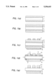
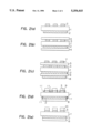
- the shape of the metal used has the following three types.
- solid metal plate metal plates 4, 5 (hereinafter referred to as "solid metal plate") involving at least a metal circuit pattern 9 and having an area wider than that as illustrated by FIGS. 1(b) and 2(b)
- a paste-like or foil-like brazing material involves at least a metal circuit pattern 9, and is disposed on a ceramic board in an area wider than that.
- the brazing material can be disposed on the whole surface of the ceramic board, and can also be disposed in the same pattern as the metal circuit pattern 9.
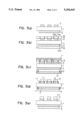
- Metal plates 12, 13 (hereinafter referred to as "half-etched metal plate") comprising a metal circuit part 13a and parts 12b, 13b other than the metal circuit part having a thickness smaller than the metal circuit part
- the parts (thinner parts) 12b, 13b other than the metal circuit are preferably formed by dissolving by chemical etching process, and a brazing material is preferably disposed in the same pattern as the metal circuit pattern 9.
- the etching resist can be coated by a simple and high productive method using a roll coater and the like.
- the etching resist can be coated on the whole surface of a ceramic board by screen printing.
- etching resist is not coated on the part (thinner part) other than the metal circuit of a half-etched metal plate, the metal circuit part and the part other the metal circuit can be easily separated from each other.
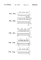
- Metal plates 14, 15 comprising a metal circuit part 15a and parts 14b, 15b other than the metal circuit in such a state as to be easily separated by applying mechanical force as illustrated by FIG. 4(b)
- a push back metal plate can be prepared, for example, in the following manner.
- a metal circuit part is pulled out from a metal plate and is inserted again to restore the original state.
- a groove is provided to the state just before a metal circuit part is slipped out.
- the major part of the groove is passed through to separate the major parts of the metal circuit part and the part other than the metal circuit.
- the thicknesses of the metal circuit part and the part other than the metal circuit may be the same or different from each other.
- the metal circuit parts may be formed by means of a press mold, a shaping machine, a milling cutter or the like, or by chemical etching.
- a brazing material should preferably be disposed in the same pattern as a metal circuit pattern, and the metal circuit pattern can be easily formed by bonding a push back metal plate with a ceramic board and then separating the metal part other than the metal circuit. An unnecessary brazing material protruded outside from the metal circuit pattern is removed by chemical liquor treatment.
- a metal circuit pattern is formed by bonding a metal plate with a ceramic board, coating an etching resist on the metal plate and then etching. When using a push back metal plate, this process is not necessary.
- Examples of the etching resist used in the present invention include an ultraviolet ray-curable type or heat-curable type resist.
- Examples of an etching solution include a ferric chloride solution, a cupric chloride solution, a sulfuric acid and a hydrogen peroxide solution when a metal plate is a copper plate or a copper alloy plate.
- a preferable etching solution is a ferric chloride solution or a cupric chloride solution.
- a ferric chloride solution is generally used.
- "Unnecessary brazing material” in the present invention means a brazing material present between metal circuit patterns.
- Such an unnecessary brazing material is a brazing material originally present between metal circuit patterns (this is produced when a brazing material is disposed on the whole surface of a ceramic board) or a brazing material protruded between metal circuit patterns when bonding a metal plate.
- the ingredients of the unnecessary brazing material include not only ingredients present at the time of preparing the brazing material but also a nitride layer produced by reaction of an active metal ingredient of the brazing material and ceramics or an alloy layer produced by reaction of metal and ceramics.
- Examples of a chemical liquor used in the present invention to remove the unnecessary brazing material include hydrofluoric acid alone, a mixed acid of hydrofluoric acid with an inorganic acid such as nitric acid, sulfuric acid or hydrochloric acid, aqua regia, a sodium hydroxide solution and a potassium hydroxide solution, and are appropriately selected depending on the ingredients of the unnecessary brazing material.
- a preferable chemical liquor is hydrofluoric acid alone or a mixed acid of hydrofluoric acid and hydrochloric acid.
- a preferable concentration is from 2 to 55% by weight
- a mixed acid preferably comprises form 2 to 40% by weight of hydrofluoric acid and from 1 to 15% by weight of an inorganic acid such as hydrochloric acid.
- the unnecessary brazing material is removed by dipping a bonded product of a metal plate and a ceramic board in the chemical liquor or by spraying the chemical liquor on the above bonded product like a shower.
- a chemical liquor may be used alone, or many kinds of chemical liquors may be used alternatively.
- the temperature of the chemical liquor is preferably raised to generally from 40° to 95° C. when used.
- the most preferable method comprises applying ultrasonic wave at the same time as the chemical liquor treatment and/or in the washing step using water, a solvent, an alkaline degreased liquor or the like after the chemical liquor treatment, thereby enabling the time required for removing unnecessary brazing material shorter.
- Ceramic board aluminum nitride board
- Brazing material paste Ag-Cu-Zr system Ag-Cu-Zr-TiH 2 system Ag-Cu-TiH 2 AlN system
- Method for removing unnecessary brazing material hydrofluoric acid or a mixed acid is used as a chemical liquor and ultrasonic vibration is applied.
- the reason why an aluminum nitride board is particularly preferable is that it has a high thermal conductivity and a thermal expansion coefficient similar to those of silicon, and the reason why a copper plate is particularly preferable, is that it has an excellent electrical conductivity.
- this brazing material is somewhat poor in the bonding strength of a copper plate and an aluminum nitride board, but has a satisfactory practical strength.
- the productivity is very high since the removability of the unnecessary brazing material with the above mentioned chemical liquor is remarkably excellent.
- the wetting property between a copper plate and a brazing material is also excellent.
- the amount of the Zr ingredient used is preferably from 4 to 35 parts by weight, more preferably from 10 to 30 parts by weight to 100 parts by weight in total of the Ag ingredient and the Cu ingredient.
- This brazing material provides both advantages at the same time, i.e. an advantage of having a good wetting property between a copper plate and a brazing material, which is the merit of Zr, and an advantage of having a good bonding strength between a copper plate and an aluminum nitride board, which is the merit of Ti.
- This brazing material provides a satisfactory bonding strength between a copper plate and an aluminum nitride board, and the protrusion of the brazing material paste between metal circuit patterns hardly occurs.
- TiH 2 is used in an amount of from 5 to 30 parts by weight and AlN is used in an amount of from 0.5 to 10 parts by weight. AlN is used preferably in proportion to the amount of TiH 2 .
- the Ag ingredient is from 60 to 85% by weight, and the Cu ingredient is from 40 to 15% by weight.
- the eutectic composition of 72% by weight of Ag ingredient and 28% by weight of Cu ingredient or its close composition is preferable.
- the present invention is illustrated with reference to the drawings taking a power semiconductor module board as an example.
- FIGS. 1 and 2 illustrate an example of using a solid metal plate as a metal plate
- FIG. 3 illustrates an example of using a half-etched metal plate
- FIG. 4 illustrating an example of using a push back metal plate.
- brazing materials 2 and 3 are disposed on a ceramic board 1.
- the brazing material is a paste
- examples of a disposing method include a screen printing method and a roll coater method, but the later method is preferable in respect of productivity when the paste is coated on the whole surface of the board.
- the brazing material is a foil
- the above-mentioned alloy foil or laminated product is disposed as it is.
- the other side of the ceramic board is coated with the brazing material 3 in substantially whole area (FIG. 1a), or in the same pattern as the metal circuit (hereinafter referred to as "bonding pattern A") or in partly the same pattern as a part of the metal circuit (hereinafter referred to as "bonding pattern B”) (FIG. 2a, FIG. 3a and FIG. 4a illustrate bonding pattern A).
- a solid metal plate 4 having an area sufficient to cover the brazing material i.e. having the same size or larger than the ceramic board, is disposed on the brazing material-disposed surface corresponding to substantially the whole area of the ceramic board.
- a solid metal plate 5 of the same size is disposed on the other side of the ceramic board to form a metal circuit 10 (FIG. 1b, FIG. 2b), but in the example of FIG. 2 it is not always necessary to use a solid metal plate but only to use a metal plate having an area sufficient to cover bonding pattern A or bonding pattern B or having an area larger than bonding pattern A or bonding pattern B.
- a copper plate used as a metal plate should preferably be a copper plate containing no oxygen.
- FIG. 3b illustrates the disposition of half-etched metal plates 12, 13, and FIG. 4b illustrates the disposition of push back metal plates 14, 15.
- processed metal plates such as a half-etched metal plate 12 and a push back metal plate 14 are disposed on the surface where the metal circuit 10 is not formed, but a solid metal plate may be used in place of these processed metal plates in the present invention.
- the etching resist 7 should accurately correspond to the disposed position of a brazing material (bonding pattern A), and it is necessary to pay attention for making this accurate correspondence.
- the bonding pattern A and the metal circuit are the same, but the present invention is not limited thereto.
- a metal circuit having a shape different from bonding pattern B and also having a non-bonded part can be easily prepared by forming an etching resist to involve bonding pattern B and also to cover a metal plate part where a brazing material is not disposed.
- the merit of forming the non-bonded part as mentioned above is that damages of a ceramic board caused by expansion-shrinkage of the metal part produced by heat cycle of electric conduction-suspension can be prevented by connecting an outer electrode with the non-bonded part when the outer electrode is connected with the metal circuit on the board.
- a metal plate in order to form a non-bonded part, a metal plate must be specially processed in such a manner as not to bring a ceramic board in contact with a part of a metal plate corresponding to the non-bonded part, and it is necessary to dispose the metal plate accurately on the specified position.
- such a step is not necessary.
- an etching resist 7 is preferably coated by a roll coater. Because a thinner part 13b other than a metal circuit is not coated even when the etching resist is coated on the whole surface of the half-etched metal plate by the roll coater, and therefore the thinner part can be removed easily, thus raising productivity. Also, when a solid metal plate is disposed on the other side where a metal circuit is not formed, it is preferable to coat an etching resist on the same surface by screen printing.
- This stage of the example of FIG. 1 is the state when unnecessary brazing materials 11 such as the originally disposed brazing material, its alloy layer and its nitride layer remain between metal circuit patterns 9.
- the essential feature of the present invention resides in this step.
- the ceramic boards obtained by the examples of FIGS. 2 to 3 have metal circuit patterns 9 at this stage, but sometimes have unnecessary brazing materials 11 protruded from metal circuit patterns 9 (FIG. 2d, FIG. 3d, FIG. 4d), which sometimes cause short-circuits.
- unnecessary brazing materials 11 particularly conductive ingredients such as a metal layer containing a small amount of an active metal ingredient of the upper layer and an alloy layer-nitride layer containing a large amount of an active metal ingredient of the lower layer, remain between metal circuit-patterns 9 (FIG. 1d), and therefore these must be removed to form a metal circuit 10.
- the treating time varies depending on the kind of the brazing materials and the type of a chemical liquor used.
- the treating time is from 5 to 20 minutes for Ag-Cu-Zr system brazing material, from 10 to 30 minutes for Ag-Cu-Zr-TiH 2 system brazing material and from 10 to 30 minutes for Ag-Cu-TiH 2 -AlN system brazing material.
- the present invention is further illustrated by the following Examples.
- brazing material pastes were prepared by mixing 72 parts of silver powder, 28 parts of copper powder, 4 parts, 20 parts or 35 parts of metal zirconium powder and 15 parts of terpinenol in weight ratio.
- Each of these pastes was coated on the whole surface of both sides of an aluminum nitride board of 60 mm ⁇ 30 mm ⁇ 0.65 mm t by a roll coater.
- the coated amount was 12.0 mg/cm 2 for the case of containing 4 parts of metal zirconium powder (Examples 1 and 2), 7.5 mg/cm 2 for the case of containing 20 parts of metal zirconium powder (Examples 3 and 4) and 5.5 mg/cm 2 for the case of containing 35 parts of metal zirconium powder (Examples 5 and 6) (FIG. 1a).
- thermosetting etching resist was coated on the copper plate of each of these bonded products (FIG. 1c), and an unnecessary part of the copper plate was removed by etching with a ferric chloride solution, then the etching resist being separated (FIG. 1d).
- the bonded products thus obtained still had unnecessary brazing materials remained between copper circuit patterns, and in order to remove the unnecessary brazing materials, five sheets each of the bonded products were treated with 10% hydrofluoric acid at 80° C. for 8 minutes in Example 1, for 12 minutes in Example 3 and for 14 minutes in Example 5.
- a ceramic circuit board was prepared in the same manner as in Example 1 by using a paste comprising 72 parts of silver powder, 28 parts of copper powder, metal zirconium powder and titanium hydride powder (ratios shown in Table 1) in weight ratio, bonding a solid copper plate with an aluminum nitride board, etching to prepare a metal circuit and removing a brazing material between patterns under the conditions shown in Table 1.
- a brazing paste was prepared by mixing 72 parts of silver powder, 28 parts of copper powder, titanium hydride powder and aluminum nitride powder in such a ratio as shown in Table 2 in weight ratio. This paste was coated on an aluminum nitride board by screen-printing in the same manner as in Example 1 in such a bonding pattern as shown in FIG. 2a. The amount of the paste coated is shown in Table 2.
- a copper plate of 60 mm ⁇ 30 mm ⁇ 0.30 mm t was disposed on both sides of the dried board in contact therewith, and was placed in a furnace.
- This sample was heated at 900° C. for 0.5 hour in a highly vacuumed atmosphere, and was cooled at a cooling rate of 3° C./min to produce a bonded product (FIG. 2b).
- a circuit pattern was formed on the copper plate of the bonded product by screen-printing a UV ray-curable etching resist in a circuit pattern, curing the printed resist (FIG. 2c), and etching in the same manner as in Example 1.
- a brazing material protruded from the periphery of the circuit pattern was removed by chemical liquor treatment under such conditions as shown in Table 2 to produce a ceramic circuit board.
- Table 14 The evaluation results are shown in Table 14.
- a brazing paste was prepared by mixing 72 parts of silver powder, 28 parts of copper powder, 9.3 parts of zirconium hydride powder and 15 parts of terpinenol.
- an aluminum nitride board and a copper plate were bonded by using this paste, and the bonded product was subjected to etching treatment and then chemical liquor treatment to produce a ceramic circuit board. Production conditions are shown in Table 3. The evaluation results are shown in Table 14.
- This Example was carried out in accordance with the steps of FIG. 2a to FIG. 2e.
- a brazing paste was prepared by mixing 72 parts of silver powder, 28 parts of copper powder, 19 parts of metal zirconium powder and 15 parts of terpinenol in weight ratio. This paste was coated on an aluminum nitride board (coated amount 10.0 mg/cm 2 ) in the same manner as in Example 12, and a solid copper plate (thickness 0.25 mm t ) was disposed thereon. The resultant product was subjected to heat treatment to produce a bonded product (bonding conditions: 940° C., 0.5 hour and cooling rate of 3° C./min). Thereafter, this bonded product was treated in the same manner as in Example 12 to produce a ceramic circuit board. The chemical liquor treatment was conducted with 30% hydrofluoric acid at 80° C. for 15 minutes. The evaluation results are shown in Table 14.
- a brazing paste was prepared by mixing 72 parts of silver powder, 28 parts of copper powder, zirconium powder, titanium powder, aluminum oxide powder and aluminum nitride powder in such ratios as shown in Table 4 in weight ratios.
- this paste and an aluminum nitride board, a ceramic circuit board using a copper plate as a metal circuit was produced in the same manner as in Example 12. The production conditions are shown in Table 4. The evaluation results are shown in Table 14.
- a paste was prepared by mixing 72 parts of silver powder, 28 parts of copper powder, and titanium hydride powder in such a ratio as shown in Table 5 in weight ratios.
- an aluminum nitride board, an aluminum oxide board and a copper board of 0.2 mm t ceramic circuit boards were produced in the same manner as in Example 1 (the paste was coated by screen-printing).
- the production conditions are shown in Table 5.
- the evaluation results are shown in Table 14.
- a brazing paste was prepared by mixing 15 parts by weight of terpinenol with 100 parts by weight of an alloy powder of silver, copper and titanium (composition: silver 72 parts, copper 28 parts and titanium 10 parts in weight ratios). This brazing paste was coated on an aluminum nitride board (Example 29) or an alumina board (Example 30) of 70 mm ⁇ 40 mm ⁇ 0.635 mm t in a bonding pattern by screen-printing (FIG. 4a).
- a push back copper plate having the same size as the board and having a thickness of 0.2 mm, the circuit part of which was struck by a press and returned to unite with the metal parts other than the circuit part, was disposed on the dried board in contact therewith in such a manner as to have the bonding pattern and the metal circuit pattern coincided, and the resultant product was heated at 880° C. for 0.5 hour in a highly vacuumed atmosphere to produce five sheets each of a bonded product (FIG. 4b).
- a metal circuit was formed by mechanically separating the parts other than the metal circuit from the bonded product (FIGS. 4c, d).
- a brazing material was protruded from the periphery of the metal circuit (FIG. 4d), and the protruded brazing material was removed with 10% hydrofluoric acid at 70° C. for 30 minutes in Example 29 and for 10 minutes in Example 30.
- the evaluation results of the ceramic circuit boards thus obtained are shown in Table 14.
- a brazing paste was prepared by mixing 100 parts by weight of an alloy powder of copper and zirconium (composition: silver 95 parts and zirconium 5 parts in weight ratios), 15 parts by weight of terpinenol and 1 part by weight of polymethylmethacrylate. This paste was coated respectively on an aluminum nitride board (Example 31) a mullite board (Example 32), an aluminum oxide board (Example 33) and a silicon nitride board (Example 34) by screen printing in a bonding pattern (the coated amount 7.0 mg/cm 2 ) (FIG. 3a).
- a half-etched copper plate having the same size as the board, which was previously modified by etching so as to have a metal circuit part of 0.3 mm t and a part other the metal circuit of 0.2 mm t was disposed on the dried board in contact therewith in such a manner as to have the paste part and the circuit part of the half-etched copper plate coincided, and the resultant product was heat-treated at 980° C. for 0.5 hour in a highly vacuumed atmosphere to produce a bonded product (FIG. 3b).
- a UV ray-curable etching resist was coated on the copper plate of the bonded product by a roll coater (FIG. 3c, the resist being deposited on the circuit part only), and the board thus coated was subjected to etching treatment in the same manner as in Example 1 to produce a metal circuit pattern.
- an unnecessary brazing material protruded from the metal circuit pattern was removed by treating with a mixed acid of 20% hydrofluoric acid and 10% nitric acid at 65° C. for 5 minutes while applying ultrasonic wave.
- a paste was prepared by mixing 100 parts by weight of an alloy powder of silver, copper and zirconium (alloy composition being shown in Table 7), 12 parts by weight of terpinenol and 1 part by weight of polyisobutyl methacrylate.
- a ceramic circuit board was produced in the same manner as in Example 1 by using this paste, an aluminum nitride board and a copper plate (thickness 0.2 mm). The production conditions are shown in Table 7. The evaluation results are shown in Table 14.
- This Example was carried out in accordance with the steps of FIG. 1a to FIG. 1e.
- a paste was prepared by mixing 100 parts by weight an alloy powder of nickel and titanium (alloy composition being shown in Table 8) and 15 parts by weight of terpinenol.
- a ceramic circuit board was produced in the same manner as in Example 1 by using this paste, an aluminum nitride board and a nickel plate (thickness 0.2 mm) (the paste was printed by screen-printing). The production conditions are shown in Table 8. The evaluation results are shown in Table 14.
- a paste was prepared by mixing 60 parts of nickel powder, 40 parts of titanium hydride powder and 12 parts of terpinenol in weight ratios.
- a ceramic circuit board was produced in the same manner as in Example 12 by using this paste, and an aluminum oxide board (Example 38) or a silicon nitride board (Example 39), and an Ni alloy plate (Ni: 80 wt %, Cu 20 wt %, thickness 0.35 mm) as a metal plate.
- the production conditions are shown in Table 9.
- the evaluation results are shown in Table 14.
- a bonded product was produced by disposing an alloy foil having the composition and thickness shown in Table 10 on the whole surface area of an aluminum nitride board of 65 mm ⁇ 45 mm ⁇ 0.635 mm t , laminating a solid copper plate of 0.25 mm t thereon and heat-treating at 920° C. for 0.5 hour in a highly vacuumed atmosphere.
- a ceramic circuit board was produced by disposing an alloy foil having the composition and thickness shown in Table 11 on an aluminum nitride board or an aluminum oxide board having the same shape as in Example 40 in a bonding pattern, laminating a push back copper plate of a thickness of 0.25 mm thereon and subjecting to the same steps as in Example 29.
- the production conditions are shown in Table 11.
- the evaluation results are shown in Table 14.
- a ceramic circuit board was produced by using an alloy foil and a metal plate shown in Table 12.
- the alloy foil was disposed on an aluminum nitride board in a bonding pattern.
- the production conditions are shown in Table 12.
- the evaluation results are shown in Table 14.
- a bonded product was produced by laminating firstly a zirconium foil and secondly an alloy foil of silver and copper (composition ratio: silver 72 parts and copper 28 parts in weight ratios) on the whole surface area of an aluminum nitride board of 60 mm ⁇ 40 mm ⁇ 0.65 mm t , disposing a copper plate of 0.3 mm t having the same shape as the laminated board and heat-treating at 940° C. for 0.3 hour in a highly vacuumed atmosphere.
- the thickness of each foil is shown in Table 13.
- a bonded product was produced by laminating firstly a titanium foil (thickness 2 ⁇ m) and secondly an alloy foil of silver and copper (the same composition as in Example 47, thickness 6 ⁇ m) on an aluminum nitride board (Example 49) or an alumina board (Example 50) in a bonding pattern, disposing a half-etched copper plate having the same size as the board, the circuit part of which has a thickness of 0.3 mm, on the laminated board in such a manner as to have the foil and the copper circuit part coincided, and heat-treating at 880° C. for 0.5 hour in a highly vacuumed atmosphere.
- Example 14 Thereafter, the bonded product was treated in the same manner as in Example 31 to form a metal circuit pattern, and a protruded brazing material was removed by treating with a mixed acid of 15% hydrofluoric acid and 20% hydrochloric acid at 70° C. for 30 minutes in Example 49 and for 5 minutes in Example 50.
- the evaluation results of the ceramic circuit board thus obtained are shown in Table 14.
Abstract
Description
                                  TABLE 1
__________________________________________________________________________
Mixed amount (parts)
                Coated
           Titanium
                amount
                     Bonding
Examples
     Zirconium
           hydride
                (mg/cm.sup.2)
                     condition
                            Chemical liquor treatment
__________________________________________________________________________
7    2     25   6.0  880° C.
                            Hydrofluoric acid
                                        →
                                          Hydrochloric acid
                     0.2 hr (70° C., 15%), ultrasonic
                                          (55° C., 10%)
                     Cooling rate
                            wave applied 10 minutes
                                          15 minutes
8    2     2    8.0  2° C./min
                            Hydrofluoric acid
                                        →
                                          Hydrochloric acid
                            (70° C., 15%), ultrasonic
                                          (55° C., 10%)
                            wave applied 5 minutes
                                          15 minutes
9    25    1    7.5         Hydrofluoric acid
                                        →
                                          Hydrochloric acid
                            (70° C., 5%), ultrasonic
                                          (55° C., 10%)
                            wave applied 5 minutes
                                          15 minutes
10   25    10   5.5         Hydrofluoric acid
                                        →
                                          Hydrochloric acid
                            (70° C., 15%), ultrasonic
                                          (55° C., 10%)
                            wave applied 10 minutes
                                          15 minutes
11   13    5    8.0         Hydrofluoric acid
                                        →
                                          Hydrochloric acid
                            (70° C., 15%), ultrasonic
                                          (55° C., 10%)
                            wave applied 5 minutes
                                          15 minutes
__________________________________________________________________________
 Note: When mixing a paste, 15 parts of terpinenol and 1 part of
 polyisobutylmethacrylate were added.
                                  TABLE 2
__________________________________________________________________________
Mixed amount (parts)
                Coated
     Titanium
          Aluminum
                amount
Examples
     hydride
          nitride
                (mg/cm.sup.2)
                     Chemical liquor treatment
__________________________________________________________________________
12   5    0.5   12.5 Hydrofluoric acid (65° C., 30%) 15 minutes
13   20   1     9.0  Hydrofluoric acid (65° C., 30%) 15 minutes
14   25   5     8.0  Mixed acid of hydrofluoric acid 25% and
                     hydrochloric acid 15% (65° C.) 20 minutes
15   30   10    10.5 Mixed acid of hydrofluoric acid 25% and
                     hydrochloric acid 15% (65° C.) 20
__________________________________________________________________________
                     minutes
 Note: When mixing a paste, 15 parts of terpinenol was added.
              TABLE 3
______________________________________
       Coated
       amount   Bonding    Chemical liquor
Examples
       (mg/cm.sup.2)
                condition  treatment
______________________________________
16     5.5      940° C.
                           Hydrofluoric acid (80° C.,
                0.5 hr     30%) 20 minutes
17     5.5      Cooling rate
                           Hydrofluoric acid (80° C.,
                3° C./min
                           30%) 10 minutes
18     7.5                 Hydrofluoric acid (80° C.,
                           30%) 20 minutes
19     7.5                 Hydrofluoric acid (80° C.,
                           30%) 10 minutes
______________________________________
                                  TABLE 4
__________________________________________________________________________
Mixed amount (parts)        Coated
                Aluminum
                      Aluminum
                            amount
                                 Bonding
Examples
     Zirconium
           Titanium
                oxide nitride
                            (mg/cm.sup.2)
                                 condition
                                        Chemical liquor
__________________________________________________________________________
                                        treatment
21   5     13   0.2   0     8.0  950° C.
                                        Hydrofluoric
                                               →
                                                 Sulfuric
                                 0.2 hr acid     acid
                                 Cooling rate
                                        (80° C.,
                                                 (70° C., 10%)
                                 3° C./min
                                        10 minutes
                                                 15 minutes
22   5     13   0     5     8.0         Hydrofluoric
                                               →
                                                 Sulfric
                                        acid     acid
                                        (80° C.,
                                                 (70° C., 10%)
                                        10 minutes
                                                 15 minutes
__________________________________________________________________________
 Note: A paste was modified by adding 12 parts of terpinenol and 0.5 part
 of polymethylmethacrylate.
                                  TABLE 5
__________________________________________________________________________
             Mixed amount
             of titanium
                     Coated
             hydride amount
                          Bonding
Examples
     Ceramic board
             (parts) (mg/cm.sup.2)
                          condition
                                 Chemical liquor treatment
__________________________________________________________________________
23   AlN     10      10.5 900° C.
                                 Hydrofluoric acid (80° C., 30%)
                                 8
                          0.5 hr minutes, ultrasonic wave applied
24   AlN     19      7.0  Cooling rate
                                 Hydrofluoric acid (80° C., 30%)
                                 12
                          2° C./min
                                 minutes, ultrasonic wave applied
25   Al.sub.2 O.sub.3
             5       6.0         Hydrofluoric acid (80° C., 30%)
                                 5
                                 minutes, ultrasonic wave applied
26   Al.sub.2 O.sub.3
             10      6.0         Hydrofluoric acid (80° C., 30%)
                                 5
                                 minutes, ultrasonic wave
__________________________________________________________________________
                                 applied
 Note: A paste was modified by adding 15 parts of terpinenol.
                                  TABLE 6
__________________________________________________________________________
          Coated
     Ceramic
          amount
               Bonding
Examples
     board
          (mg/cm.sup.2)
               condition
                      Chemical liquor treatment
__________________________________________________________________________
27   AlN  9.0  980° C.
                      Hydrofluoric acid
                                  →
                                    Ultrasonic wave applied
               0.5 hr (85° C., 10%) 5 minutes
                                    during washing with water
28   Al.sub.2 O.sub.3
          9.0  Cooling rate
                      Hydrofluoric acid (85° C., 10%) 5 minutes
               2° C./min
__________________________________________________________________________
                                  TABLE 7
__________________________________________________________________________
Composition of Alloy
                   Coated
(parts by weight)  amount
                        Bonding
Examples
     Silver
         Copper
             Zirconium
                   (mg/cm.sup.2)
                        condition
                               Chemical liquor treatment
__________________________________________________________________________
35   72  28  5     11.0 920° C.
                               Hydrofluoric acid
                                        →
                                          Ultrasonic wave
                        0.3 hr (80° C., 15%)
                                          applied during
                        Cooling rate
                               3 minutes  washing with
                        2° C./min  water
36   72  28  20    8.0         Hydrofluoric acid
                                        →
                                          Ultrasonic wave
                               (80° C., 15%)
                                          applied during
                               6 minutes  washing with
                                          water
__________________________________________________________________________
                                  TABLE 8
__________________________________________________________________________
Composition of Alloy
                Coated
(parts by weight)
                amount
                     Bonding
Examples
     Nickel
          Titanium
                (mg/cm.sup.2)
                     condition
                            Chemical liquor treatment
__________________________________________________________________________
37   60   40    7.0  1150° C.
                            Sodium hydroxide solution
                     0.5 hr (45° C., 20%) 5 minutes
                     Temperature-
                     descending
                     speed
                     2° C./min
__________________________________________________________________________
                                  TABLE 9
__________________________________________________________________________
             Coated
             amount
                  Bonding
Examples
     Ceramic board
             (mg/cm.sup.2)
                  condition
                         Chemical liquor treatment
__________________________________________________________________________
38   Al.sub.2 O.sub.3
             8.0  1180° C.
                         Potassium hydroxide solution
                  0.3 hr (50° C., 15%) 5 minutes
39   Si.sub.3 N.sub.4
             8.0  Temperature-
                         Potassium hydroxide solution
                  descending
                         (50° C., 15%) 5 minutes
                  speed
                  2° C./min
__________________________________________________________________________
                                  TABLE 10
__________________________________________________________________________
Composition of Alloy
                   Thickness of
(parts by weight)  alloy foil
Examples
     Silver
         Copper
             Zirconium
                   μm) Chemical liquor treatment
__________________________________________________________________________
40   72  28   5    10     Hydrofluoric acid →
                                     Ultrasonic wave
                          (80° C., 10%)
                                     applied during
                          4 minutes  washing with water
41   72  28  10    10     Hydrofluoric acid →
                                     Ultrasonic wave
                          (800° C., 10%)
                                     applied during
                          6 minutes  washing with water
42   72  28  30     9     Hydrofluoric acid →
                                     Ultrasonic wave
                          (800 C., 10%)
                                     applied during
                          7 minutes  washing with water
__________________________________________________________________________
                                  TABLE 11
__________________________________________________________________________
          Composition of Alloy
                        Thickness
Ceramic   (parts by weight)
                        of alloy
                              Bonding
Examples
     board
          Silver
              Copper
                  Titanium
                        foil (μm)
                              condition
                                     Chemical liquor treatment
__________________________________________________________________________
43   AlN  72  28  15    9     900° C.
                                     Hydrofluoric acid (70° C.,
                              0.2 hr 10%) 30 minutes
44   Al.sub.2 O.sub.3
          72  28   5    9     Temperature-
                                     Hydrofluoric acid (70° C.,
                              descending
                                     10%) 10 minutes
                              speed
                              2° C./min
__________________________________________________________________________
                                  TABLE 12
__________________________________________________________________________
           Composition of Alloy
                         Thickness
Metal      (parts by weight)
                         of alloy
                              Bonding
Examples
     plate Copper
               Nickel
                   Titanium
                         foil (μm)
                              condition
                                     Chemical liquor treatment
__________________________________________________________________________
45   Copper
           95   0   5    15   980° C.
                                     Sodium hydroxide solution
     alloy                    0.3 hr (45° C., 20%) 5 minutes
     plate                    Temperature-
     (Cu 80                   descending
     wt %, Ni                 speed
     20 wt %)                 2° C./min
46   Nickel
            0  60  40     9   1150° C.
                                     Aqua regia (55° C., 30%) 3
     alloy                    0.5 hr minutes
     Plate                    Temperature-
     (Ni 80                   desending
     wt %, Cu                 speed
     20 wt %)                 2° C./min
__________________________________________________________________________
              TABLE 13
______________________________________
             Thickness of
                        Thickness of
             zirconium foil
                        silver/copper
Examples     (μm)    alloy foil
______________________________________
47           2          11
48           4           7
______________________________________
TABLE 14
__________________________________________________________________________
Soldering material for bonding
Type of Coated
Form of
soldering
amount Peeling strength (1
soldering
material and
of sheet, 1 point, total
5
Ex-
Type of material
composition
paste points, kg/cm)
am-
Ceramic
Metal
and (parts by
(mg/ Aver-
Mini-
Maxi-
ples
board
plate
disposition
weight) cm.sup.2)
Chemical liquor treatment
age mum mum
__________________________________________________________________________
1 AlN Solid
Paste (mix-
Ag/Cu/Zr 12.0
Hydrofluoric acid (80° C.,
7.1 6.5 7.7
Cu ture) disposed
72/28/4 10%) 8 minutes
plate
on whole
surface
2 AlN Solid
Paste (mix-
Ag/Cu/Zr 12.0
Hydrofluoric acid →
Ultrasonic
7.2 6.4 7.9
Cu ture) disposed
72/28/4 (80° C., 10%)
wave applied
plate
on whole 4 minutes during washing
surface with water
3 AlN Solid
Paste (mix-
Ag/Cu/Zr 7.5 Hydrofluoric acid (80° C., 10%)
12 8.6 7.6 9.8
Cu ture) disposed
72/28/20 minutes
plate
on whole
surface
4 AlN Solid
Paste (mix-
Ag/Cu/Zr 7.5 Hydrofluoric acid →
Ultasonic
8.7 7.5 10.0
Cu ture) disposed
72/28/20 (80° C., 10%)
wave applied
plate
on whole 6 minutes during washing
surface with water
5 AlN Solid
Paste (mix-
Ag/Cu/Zr 5.5 Hydrofluoric acid (80° C., 10%)
14 7.8 6.9 9.0
Cu ture) disposed
72/28/35 minutes
plate
on whole
surface
6 AlN Solid
Paste (mix-
Ag/Cu/Zr 5.5 Hydrofluoric acid →
Ultrasonic
7.7 7.2 8.9
Cu ture) disposed
72/28/35 (80° C., 10%)
wave applied
plate
on whole 7 minutes during washing
surface with water
7 AlN Solid
Paste (mix-
Ag/Cu/Zr/TiH.sub.2
6.0 Hydrofluoric acid (70° C., 15%)
Ultra- 11.2
9.4 12.3
Cu ture) disposed
72/28/2/25 sonic wave applied 10 minutes →
plate
on whole Hydrochloric acid (55° C., 10%) 15
surface minutes
8 AlN Solid
Paste (mix-
Ag/Cu/Zr/TiH.sub.2
8.0 Hydrofluoric acid (70° C., 15%)
Ultra- 6.6 6.1 7.1
Cu ture) disposed
72/28/2/2 sonic wave applied 5 minutes →
plate
on whole Hydrochloric acid (55° C., 10%) 15
surface minutes
9 AlN Solid
Paste (mix-
Ag/Cu/Zr/TiH.sub.2
7.5 Hydrofluoric acid (70° C., 15%)
Ultra- 9.8 8.8 11.0
Cu ture) disposed
72/28/25/1 sonic wave applied 5 minutes →
plate
on whole Hydrochloric acid (55° C., 10%) 15
surface minutes
10 AlN Solid
Paste (mix-
Ag/Cu/Zr/TiH.sub.2
5.5 Hydrofluoric acid (70° C., 15%)
Ultra- 10.4
9.5 11.3
Cu ture) disposed
72/28/25/10 sonic wave applied 10 minutes →
plate
on whole Hydrochloric acid (55° C., 10%) 15
surface minutes
11 AlN Solid
Paste (mix-
Ag/Cu/Zr/TiH.sub.2
8.0 Hydrofluoric acid (70° C., 15%)
Ultra- 11.5
9.3 12.5
Cu ture) disposed
72/28/13/5 sonic wave applied 5 minutes →
plate
on whole Hydrochloric acid (55° C., 10%) 15
surface minutes
12 AlN Solid
Paste (mix-
Ag/Cu/TiH.sub.2 /
12.5
Hydrofluoric acid (65° C.,
7.6)
7.2 8.1
Cu ture) disposed
AlN 15 minutes
plate
in bonding
72/28/5/0.5
pattern
13 AlN Solid
Paste (mix-
Ag/Cu/TiH.sub.2 /
9.0 Hydrofluoric acid (65° C.,
11.4
10.7
12.2
Cu ture) disposed
AlN 15 minutes
plate
in bonding
72/28/20/1
pattern
14 AlN Solid
Paste (mix-
Ag/Cu/TiH.sub.2 /
8.0 Mixed acid of hydrofluoric acid
10.8
9.9 11.5
Cu ture) disposed
AlN and hydrochloric acid 15% (65° C.)
20
plate
in bonding
72/28/25/5 minutes
pattern
15 AlN Solid
Paste (mix-
Ag/Cu/TiH.sub.2 /
8.0 Mixed acid of hydrofluoric acid
8.9 8.5 9.4
Cu ture) disposed
AlN and hydrochloric acid 15% (65° C.)
20
plate
in bonding
72/28/30/10 minutes
pattern
16 AlN Solid
Paste (mix-
Ag/Cu/ZrH.sub.2
5.5 Hydrofluoric acid (80° C., 30%) 20
minutes 6.5 6.0 7.1
Cu ture) disposed
72/28/9.3
plate
on whole
surface
17 AlN Solid
Paste (mix-
Ag/Cu/ZrH.sub.2
5.5 Hydrofluoric acid (80° C., 30%) 10
minutes 7.0 6.4 7.5
Cu ture) disposed
72/28/9.3
plate
on whole
surface
18 AlN Solid
Paste (mix-
Ag/Cu/ZrH.sub.2
7.5 Hydrofluoric acid (80° C., 30%) 20
minutes 7.5 6.9 8.2
Cu ture) disposed
72/28/9.3
plate
on whole
surface
19 AlN Solid
Paste (mix-
Ag/Cu/ZrH.sub.2
7.5 Hydrofluoric acid (80° C., 30%) 10
minutes 8.1 7.3 8.6
Cu ture) disposed
72/28/9.3
plate
on whole
surface
20 AlN Solid
Paste (mix-
Ag/Cu/Zr 10.0
Hydrofluoric acid (80° C., 30%) 15
minutes 8.0 7.1 8.8
Cu ture) disposed
72/28/19
plate
in bonding
pattern
21 AlN Solid
Paste (mix-
Ag/Cu/Zr/Ti/
8.0 Hydrofluoric acid (80° C., 30%)
8.2 7.5 9.2
Cu ture) disposed
Al.sub.2 O.sub.3
minutes → sulfuric acid
(70° C. 10%)
plate
in bonding
72/28/5/13/0.2
15 minutes
pattern
22 AlN Solid
Paste (mix-
Ag/Cu/Zr/Ti/
8.0 Hydrofluoric acid (80° C., 30%)
8.4 7.9 9.6
Cu ture) disposed
AlN minutes → sulfuric acid
(70° C. 10%)
plate
in bonding
72/28/5/13/5 15 minutes
pattern
23 AlN Solid
Paste (mix-
Ag/Cu/TiH.sub.2
10.5
Hydrofluoric acid (80° C., 30%) 8
minutes 8.3 8.9 7.8
Cu ture) disposed
72/28/10 ultrasonic wave applied
plate
on whole
surface
24 AlN Solid
Paste (mix-
Ag/Cu/TiH.sub.2
7.0 Hydrofluoric acid (80° C., 30%)
11.8
10.8
13.0
Cu ture) disposed
72/28/19 minutes, ultrasonic wave applied
plate
on whole
surface
25 Al.sub.2 O.sub.3
Solid
Paste (mix-
Ag/Cu/TiH.sub.2
6.0 Hydrofluoric acid (80° C., 30%) 5
minutes, 12.0
10.5
14.1
Cu ture) disposed
72/28/5 ultrasonic wave applied
plate
on whole
surface
26 Al.sub.2 O.sub.3
Solid
Paste (mix-
Ag/Cu/TiH.sub.2
6.0 Hydrofluoric acid (80° C., 30%) 5
minutes, 9.2 8.0 10.3
Cu ture) disposed
72/28/10 ultrasonic wave applied
plate
on whole
surface
27 AlN Solid
Paste Cu/Ti 9.0 Hydrofluoric acid →
Ultrasonic
5.9 5.1 6.5
Cu (alloy)
95/5 (85° C., 10%)
wave applied
plate
disposed 5 minutes during washing
on whole with water
surface
28 Al.sub.2 O.sub.3
Solid
Paste Cu/Ti 9.0 Hydrofluoric acid (85° C., 10%) 5
minutes 7.0 6.1 8.0
Cu (alloy)
95/5
plate
disposed
on whole
surface
29 AlN Push
Paste Ag/Cu/Ti 6.0 Hydrofluoric acid (70° C., 10%)
6.1 5.5 7.0
back
(alloy)
72/28/10 minutes
Cu disposed
plate
in bonding
pattern
30 Al.sub.2 O.sub.3
Push
Paste Ag/Cu/Ti 6.0 Hydrofluoric acid (70° C., 10%)
9.3 8.1 10.5
back
(alloy)
72/28/10 minutes
Cu disposed
plate
in bonding
pattern
31 AlN Half-
Paste Cu/Zr 7.0 Mixed acid of hydrofluoric acid 20%
6.2 5.5 7.0
etched
(alloy)
95/5 nitric acid 10% (65° C.) 5
minutes,
Cu disposed ultrasonic wave applied
plate
in bonding
pattern
32 Mullite
Half-
Paste Cu/Zr 7.0 Mixed acid of hydrofluoric acid 20%
6.4 5.9 7.3
etched
(alloy)
95/5 nitric acid 10% (65° C.) 5
minutes,
Cu disposed ultrasonic wave applied
plate
in bonding
pattern
33 Al.sub.2 O.sub.3
Half-
Paste Cu/Zr 7.0 Mixed acid of hydrofluoric acid 20%
7.9 7.3 8.5
etched
(alloy)
95/5 nitric acid 10% (65° C.) 5
minutes,
Cu disposed ultrasonic wave applied
plate
in bonding
pattern
34 Si.sub.3 N.sub.4
Half-
Paste Cu/Zr 7.0 Mixed acid of hydrofluoric acid 20%
6.1 5.2 7.3
etched
(alloy)
95/5 nitric acid 10% (65° C.) 5 minutes
Cu disposed ultrasonic wave applied
plate
in bonding
pattern
35 AlN Solid
Paste Al/Cu/Zr 11.0
Hydrofluoric acid →
Ultrasonic
7.1 6.4 7.9
Cu (alloy)
72/28/5 (80° C., 15%)
wave applied
plate
disposed 3 minutes during washing
on whole with water
surface
36 AlN Solid
Paste Al/Cu/Zr 8.0 Hydrofluoric acid →
Ultrasonic
8.3 7.3 9.5
Cu (alloy)
72/28/20 (80° C., 15%)
wave applied
plate
disposed 6 minutes during washing
on whole with water
surface
37 AlN Solid
Paste Ni/Ti 7.0 NaOH (45° C., 20%) 5
6.1utes
5.3 7.2
Ni (alloy)
60/40
plate
disposed
in bonding
pattern
38 Al.sub.2 O.sub.3
Solid
Paste (mix-
Ni/TiH.sub.2
8.0 KOH (50° C., 15%) 5
6.0utes
5.1 6.8
Ni ture) disposed
60/40
plate
in bonding
pattern
39 Si.sub.3 N.sub.4
Solid
Paste (mix-
Ni/TiH.sub.2
8.0 KOH (50° C., 10%) 10
5.8utes
5.0 6.5
Ni ture) disposed
60/40
alloy
in bonding
plate
pattern
40 AlN Solid
Alloy foil
Ag/Cu/Zr 10 Hydrofluoric acid →
Ultrasonic
7.3 6.8 8.0
Cu disposed
72/28/5 (80° C., 10%)
wave applied
plate
on whole 4 minutes during washing
surface with water
41 AlN Solid
Alloy foil
Ag/Cu/Zr 10 Hydrofluoric acid →
Ultrasonic
8.0 7.5 8.6
Cu disposed
72/28/10 (80° C., 10%)
wave applied
plate
on whole 6 minutes during washing
surface with water
42 AlN Solid
Alloy foil
Ag/Cu/Zr 9 Hydrofluoric acid →
Ultrasonic
7.6 6.9 8.2
Cu disposed
72/28/30 (80° C., 10%)
wave applied
plate
on whole 7 minutes during washing
surface with water
43 AlN Push
Alloy foil
Ag/Cu/Ti 9 Hydrofluoric acid (70° C., 10%)
30 7.1 6.5 8.0
back
disposed
72/28/15 minutes
Cu in bonding
plate
pattern
44 Al.sub.2 O.sub.3
Push
Alloy foil
Ag/Cu/Ti 9 Hydrofluoric acid (70° C., 10%)
9.0 7.7 10.2
back
disposed
72/28/5 minutes
Cu in bonding
plate
pattern
45 AlN Solid
Alloy foil
Cu/Ti 15 NaOH (45° C., 20%) 5
5.9utes
6.5 5.0
cu disposed
95/5
alloy
in bonding
plate
pattern
46 AlN Solid
Alloy foil
Ni/Ti 9 Aqua regia (55° C., 30%) 3
5.8utes
6.3 5.2
Ni disposed
60/40
alloy
in bonding
plate
pattern
47 AlN Solid
Laminate
Ag/Cu/Zr Ag/ Hydrofluoric acid (80° C., 10%) 5
minutes, 8.1 7.6 8.5
Cu of Ag/Cu
-- Cu: ultrasonic wave applied
plate
alloy foil 11 μm,
and Zr foil Zr:
disposed 2 μm
on whole
surface
48 AlN Solid
Laminate
Ag/Cu/Zr Ag/ Hydrofluoric acid (80° C., 10%) 7
minutes, 7.7 7.1 8.8
Cu of Ag/Cu
-- Cu: ultrasonic wave applied
plate
alloy foil 7 μm,
and Zr foil Zr:
disposed 4 μm
on whole
surface
49 AlN Half-
Laminate
Ag/Cu/Ti Ag/ Mixed acid of hydrofluoric acid
7.0%)
6.6 7.9
etched
of Ag/Cu
-- Cu: and hydrochloric acid (20%) (70°
C.)
Cu alloy foil 6 μm
30 minutes
plate
and Ti foil Ti:
disposed 2 μm
on whole
surface
50 Al.sub.2 O.sub.3
Half-
Laminate
Ag/Cu/Ti Ag/ Mixed acid of hydrofluoric acid
9.0%)
7.7 10.0
etched
of Ag/Cu
-- Cu: and hydrochloric acid (20%) (70°
C.)
Cu alloy foil 6 μm,
5 minutes
plate
and Ti foil Ti:
disposed 2 μm
in bonding
pattern
__________________________________________________________________________
*It was not recognized that any soldering material ingredient remained
between patterns in any of the Examples.
Claims (25)
Priority Applications (1)
| Application Number | Priority Date | Filing Date | Title |
|---|---|---|---|
| US08/000,584 US5354415A (en) | 1990-04-16 | 1993-01-04 | Method for forming a ceramic circuit board |
Applications Claiming Priority (5)
| Application Number | Priority Date | Filing Date | Title |
|---|---|---|---|
| JP2-97523 | 1990-04-16 | ||
| JP9752390 | 1990-04-16 | ||
| PCT/JP1990/001502 WO1991016805A1 (en) | 1990-04-16 | 1990-11-16 | Ceramic circuit board |
| US77821191A | 1991-12-16 | 1991-12-16 | |
| US08/000,584 US5354415A (en) | 1990-04-16 | 1993-01-04 | Method for forming a ceramic circuit board |
Related Parent Applications (1)
| Application Number | Title | Priority Date | Filing Date |
|---|---|---|---|
| US77821191A Continuation | 1990-04-16 | 1991-12-16 |
Publications (1)
| Publication Number | Publication Date |
|---|---|
| US5354415A true US5354415A (en) | 1994-10-11 |
Family
ID=14194619
Family Applications (1)
| Application Number | Title | Priority Date | Filing Date |
|---|---|---|---|
| US08/000,584 Expired - Lifetime US5354415A (en) | 1990-04-16 | 1993-01-04 | Method for forming a ceramic circuit board |
Country Status (4)
| Country | Link |
|---|---|
| US (1) | US5354415A (en) |
| EP (1) | EP0480038B1 (en) |
| DE (1) | DE69031039T2 (en) |
| WO (1) | WO1991016805A1 (en) |
Cited By (43)
| Publication number | Priority date | Publication date | Assignee | Title |
|---|---|---|---|---|
| US5807626A (en) * | 1995-07-21 | 1998-09-15 | Kabushiki Kaisha Toshiba | Ceramic circuit board |
| EP0915512A2 (en) * | 1997-11-07 | 1999-05-12 | Denki Kagaku Kogyo Kabushiki Kaisha | Ceramic substrate having a metal circuit |
| US5998043A (en) * | 1996-02-05 | 1999-12-07 | Sumitomo Electric Industries, Ltd. | Member for semiconductor device using an aluminum nitride substrate material, and method of manufacturing the same |
| US6106960A (en) * | 1995-02-09 | 2000-08-22 | Ngk Insulators, Ltd. | Joined articles, corrosion-resistant joining materials and process for producing joined articles |
| US6221511B1 (en) * | 1997-03-12 | 2001-04-24 | Dowa Mining Co. Ltd. | Metal-ceramic composite substrates, producing methods thereof and brazing materials for use in such method |
| US6426154B1 (en) * | 1999-09-28 | 2002-07-30 | Kabushiki Kaisha Toshiba | Ceramic circuit board |
| EP1246514A2 (en) * | 2001-03-29 | 2002-10-02 | Ngk Insulators, Ltd. | Circuit board and method for producing the same |
| US6475401B1 (en) * | 1999-06-22 | 2002-11-05 | Jurgen Schulz-Harder | Process for the manufacture of substrates with textured metalizations and holding and fastening elements for use in this process |
| US6485816B2 (en) * | 2000-01-31 | 2002-11-26 | Ngk Insulators, Ltd. | Laminated radiation member, power semiconductor apparatus, and method for producing the same |
| EP1298970A2 (en) * | 2001-09-28 | 2003-04-02 | Dowa Mining Co., Ltd. | Method for producing metal/ceramic bonding circuit board |
| US20030102553A1 (en) * | 2001-02-22 | 2003-06-05 | Shuhei Ishikawa | Member for electronic circuit, method for manufacturing the member, and electronic part |
| US20040035693A1 (en) * | 2002-08-26 | 2004-02-26 | Shao-Pin Ru | Method for removing voids in a ceramic substrate |
| EP1408725A1 (en) * | 2001-08-09 | 2004-04-14 | Dowa Mining Co., Ltd. | Process for producing ceramic circuit boards |
| US20040112571A1 (en) * | 2002-11-01 | 2004-06-17 | Cooligy, Inc. | Method and apparatus for efficient vertical fluid delivery for cooling a heat producing device |
| US20040191558A1 (en) * | 2003-03-28 | 2004-09-30 | Ngk Insulators, Ltd. | Heat spreader module and method of manufacturing same |
| US20050227473A1 (en) * | 2004-03-24 | 2005-10-13 | Tosoh Corporation | Etching composition and method for etching a substrate |
| US20060108601A1 (en) * | 2004-11-25 | 2006-05-25 | Fuji Electric Holdings Co., Ltd. | Insulating substrate and semiconductor device |
| US20070058349A1 (en) * | 2005-09-09 | 2007-03-15 | Ngk Insulators, Ltd. | Heat spreader module and method of manufacturing same |
| US20070274047A1 (en) * | 2004-04-05 | 2007-11-29 | Mitsubishi Materials Corporation | Ai/Ain Joint Material, Base Plate For Power Module, Power Module, And Manufacturing Method Of Ai/Ain Joint Material |
| US20090000771A1 (en) * | 2007-05-02 | 2009-01-01 | James Horn | Micro-tube/multi-port counter flow radiator design for electronic cooling applications |
| US20100035024A1 (en) * | 2008-08-05 | 2010-02-11 | Cooligy Inc. | Bonded metal and ceramic plates for thermal management of optical and electronic devices |
| EP1965423A3 (en) * | 2007-02-28 | 2010-06-16 | Dowa Metaltech Co., Ltd. | Metal/ceramic bonding substrate and brazing filler metal for use therein |
| US20110123931A1 (en) * | 2009-11-20 | 2011-05-26 | Holy Stone Enterprise Co., Ltd. | High-precision ceramic substrate preparation process |
| US20110120969A1 (en) * | 2009-11-20 | 2011-05-26 | Holy Stone Enterprise Co., Ltd. | Process of manufacturing ceramic substrate |
| US20120119349A1 (en) * | 2009-07-24 | 2012-05-17 | Toshiba Materials Co., Ltd. | Insulation sheet made from silicon nitride, and semiconductor module structure using the same |
| US20120321805A1 (en) * | 2010-03-02 | 2012-12-20 | Tokuyama Corporation | Production method of metallized substrate |
| US8464781B2 (en) | 2002-11-01 | 2013-06-18 | Cooligy Inc. | Cooling systems incorporating heat exchangers and thermoelectric layers |
| US8602092B2 (en) | 2003-07-23 | 2013-12-10 | Cooligy, Inc. | Pump and fan control concepts in a cooling system |
| US20140338192A1 (en) * | 2011-12-23 | 2014-11-20 | Inktec Co., Ltd. | Method for manufacturing a metal printed circuit board |
| US20150208496A1 (en) * | 2012-02-01 | 2015-07-23 | Mitsubishi Materials Corporation | Power module substrate, power module substrate with heat sink, power module, method of manufacturing power module substrate, and copper member-bonding paste |
| EP2861046A4 (en) * | 2013-08-15 | 2015-08-05 | Hitachi Metals Ltd | Ceramic circuit board manufacturing method, and ceramic circuit board |
| CN104838488A (en) * | 2012-12-06 | 2015-08-12 | 三菱综合材料株式会社 | Substrate for power modules, substrate with heat sink for power modules, power module, method for producing substrate for power modules, paste for copper plate bonding, and method for producing bonded body |
| US20150284296A1 (en) * | 2012-11-20 | 2015-10-08 | Tokuyama Corporation | Metal/ceramic bonding substrate and method for producing same |
| US9297571B1 (en) | 2008-03-10 | 2016-03-29 | Liebert Corporation | Device and methodology for the removal of heat from an equipment rack by means of heat exchangers mounted to a door |
| US9301390B2 (en) | 2009-03-30 | 2016-03-29 | Tokuyama Corporation | Process for producing metallized substrate, and metallized substrate |
| EP2108190B1 (en) * | 2007-01-10 | 2017-12-06 | OSRAM GmbH | Electronic component module and method for production thereof |
| EP3370488A1 (en) * | 2017-03-03 | 2018-09-05 | Dowa Metaltech Co., Ltd. | Method for producing metal/ceramic circuit board |
| US20190002359A1 (en) * | 2015-12-22 | 2019-01-03 | Heraeus Deutschland GmbH & Co. KG | Thick-film paste mediated ceramics bonded with metal or metal hybrid foils |
| US20190132956A1 (en) * | 2016-06-23 | 2019-05-02 | Mitsubishi Materials Corporation | Method for manufacturing insulated circuit board, insulated circuit board, and thermoelectric conversion module |
| CN110993485A (en) * | 2019-11-27 | 2020-04-10 | 江苏富乐德半导体科技有限公司 | Surface passivation method of silicon nitride ceramic copper-clad substrate |
| CN114105668A (en) * | 2021-12-19 | 2022-03-01 | 辽宁伊菲科技股份有限公司 | Raw material preparation method and equipment for preventing brazing delamination of silicon nitride integrated circuit board |
| US20220192015A1 (en) * | 2019-03-29 | 2022-06-16 | Kyocera Corporation | Wiring board, electronic device package, and electronic device |
| US11393738B2 (en) * | 2016-01-22 | 2022-07-19 | Mitsubishi Materials Corporation | Bonded body, power module substrate, power module, method for manufacturing bonded body, and method for manufacturing power module substrate |
Families Citing this family (5)
| Publication number | Priority date | Publication date | Assignee | Title |
|---|---|---|---|---|
| JPH09181423A (en) * | 1990-04-16 | 1997-07-11 | Denki Kagaku Kogyo Kk | Ceramic circuit board |
| JP4394477B2 (en) * | 2003-03-27 | 2010-01-06 | Dowaホールディングス株式会社 | Method for producing metal / ceramic bonding substrate |
| JP6631333B2 (en) * | 2016-03-11 | 2020-01-15 | 三菱マテリアル株式会社 | Method for manufacturing power module substrate |
| DE102020111697A1 (en) * | 2020-04-29 | 2021-11-04 | Rogers Germany Gmbh | Carrier substrate and method for producing a carrier substrate |
| DE102020111700A1 (en) * | 2020-04-29 | 2021-11-04 | Rogers Germany Gmbh | Carrier substrate and method for producing a carrier substrate |
Citations (30)
| Publication number | Priority date | Publication date | Assignee | Title |
|---|---|---|---|---|
| JPS513101A (en) * | 1974-06-25 | 1976-01-12 | Sharp Kk | DENPASHA HEIYOBAN |
| JPS54103568A (en) * | 1978-01-31 | 1979-08-15 | Matsushita Electric Works Ltd | Method of forming electric circuit |
| JPS5541744A (en) * | 1978-09-19 | 1980-03-24 | Tokyo Shibaura Electric Co | Method of manufacturing printed circuit board |
| US4227039A (en) * | 1977-10-24 | 1980-10-07 | Asahi Kasei Kogyo Kabushiki Kaisha | Thin-film microcircuit board |
| JPS5750490A (en) * | 1980-09-11 | 1982-03-24 | Nippon Electric Co | Method of producing hybrid circuit board |
| US4435611A (en) * | 1980-03-24 | 1984-03-06 | Sony Corporation | Conductive paste |
| EP0115158A2 (en) * | 1982-12-23 | 1984-08-08 | Kabushiki Kaisha Toshiba | Substrate for semiconductor module |
| JPS59229892A (en) * | 1983-06-13 | 1984-12-24 | 株式会社東芝 | Method of producing printed board |
| EP0153618A2 (en) * | 1984-02-24 | 1985-09-04 | Kabushiki Kaisha Toshiba | Method for preparing highly heat-conductive substrate and copper wiring sheet usable in the same |
| JPS60195068A (en) * | 1984-03-16 | 1985-10-03 | 田中貴金属工業株式会社 | Ceramic bonding method |
| JPS6142192A (en) * | 1984-08-03 | 1986-02-28 | オ−ケ−プリント配線株式会社 | Method of producing ceramic substrate |
| JPS6182493A (en) * | 1984-09-29 | 1986-04-26 | 株式会社東芝 | Manufacture of ceramic circuit board |
| JPS61121489A (en) * | 1984-11-19 | 1986-06-09 | 株式会社東芝 | Cu wiring sheet for manufacture of substrate |
| JPS61158423A (en) * | 1984-12-28 | 1986-07-18 | Toyobo Co Ltd | Orienting film manufacturing method |
| US4647477A (en) * | 1984-12-07 | 1987-03-03 | Kollmorgen Technologies Corporation | Surface preparation of ceramic substrates for metallization |
| JPS62151581A (en) * | 1985-12-26 | 1987-07-06 | Toshiba Corp | Treating material for metallic surface |
| JPS62264689A (en) * | 1986-05-13 | 1987-11-17 | 同和鉱業株式会社 | Manufacture of metal-ceramics junction unit with circuit |
| US4712161A (en) * | 1985-03-25 | 1987-12-08 | Olin Corporation | Hybrid and multi-layer circuitry |
| JPS63160393A (en) * | 1986-12-24 | 1988-07-04 | ロ−ム株式会社 | Manufacture of circuit board |
| JPS63169348A (en) * | 1986-12-29 | 1988-07-13 | Teikoku Piston Ring Co Ltd | Amorphous alloy foil for jointing ceramics |
| JPS6424078A (en) * | 1987-07-17 | 1989-01-26 | Nippon Steel Corp | Method for joining ceramic to metal |
| JPS6442370A (en) * | 1987-08-08 | 1989-02-14 | Toshiba Corp | Method for joining ceramics and metal |
| JPS6454798A (en) * | 1987-08-26 | 1989-03-02 | Hitachi Ltd | Manufacture of ceramic substrate |
| JPH01313968A (en) * | 1988-06-13 | 1989-12-19 | Tanaka Kikinzoku Kogyo Kk | Lead pin for ceramic package |
| US5019187A (en) * | 1988-03-04 | 1991-05-28 | Kabushiki Kaisha Toshiba | Brazing paste for bonding metal and ceramic |
| US5025116A (en) * | 1989-01-27 | 1991-06-18 | Nippon Cmk Corp. | Printed wiring board having electromagnetic wave shielding layer |
| US5036167A (en) * | 1988-09-07 | 1991-07-30 | Toshiba Lighting & Technology Corporation | Board for hybrid integrated circuit |
| US5058799A (en) * | 1986-07-24 | 1991-10-22 | Zsamboky Kalman F | Metallized ceramic substrate and method therefor |
| US5110384A (en) * | 1989-04-21 | 1992-05-05 | E. I. Du Pont De Nemours And Company | Process for making electrically conductive patterns |
| US5240551A (en) * | 1990-10-05 | 1993-08-31 | Kabushiki Kaisha Toshiba | Method of manufacturing ceramic circuit board |
Family Cites Families (4)
| Publication number | Priority date | Publication date | Assignee | Title |
|---|---|---|---|---|
| JPS508179B1 (en) * | 1970-06-26 | 1975-04-02 | ||
| JPS5815955B2 (en) * | 1975-03-14 | 1983-03-28 | 三洋電機株式会社 | Concerns about the construction of the government |
| JPS61158423U (en) * | 1985-03-22 | 1986-10-01 | ||
| JPH01230290A (en) * | 1988-03-09 | 1989-09-13 | Mitsubishi Electric Corp | Forming method for thick film circuit |
-
1990
- 1990-11-16 DE DE69031039T patent/DE69031039T2/en not_active Expired - Fee Related
- 1990-11-16 EP EP90916807A patent/EP0480038B1/en not_active Expired - Lifetime
- 1990-11-16 WO PCT/JP1990/001502 patent/WO1991016805A1/en active IP Right Grant
-
1993
- 1993-01-04 US US08/000,584 patent/US5354415A/en not_active Expired - Lifetime
Patent Citations (30)
| Publication number | Priority date | Publication date | Assignee | Title |
|---|---|---|---|---|
| JPS513101A (en) * | 1974-06-25 | 1976-01-12 | Sharp Kk | DENPASHA HEIYOBAN |
| US4227039A (en) * | 1977-10-24 | 1980-10-07 | Asahi Kasei Kogyo Kabushiki Kaisha | Thin-film microcircuit board |
| JPS54103568A (en) * | 1978-01-31 | 1979-08-15 | Matsushita Electric Works Ltd | Method of forming electric circuit |
| JPS5541744A (en) * | 1978-09-19 | 1980-03-24 | Tokyo Shibaura Electric Co | Method of manufacturing printed circuit board |
| US4435611A (en) * | 1980-03-24 | 1984-03-06 | Sony Corporation | Conductive paste |
| JPS5750490A (en) * | 1980-09-11 | 1982-03-24 | Nippon Electric Co | Method of producing hybrid circuit board |
| EP0115158A2 (en) * | 1982-12-23 | 1984-08-08 | Kabushiki Kaisha Toshiba | Substrate for semiconductor module |
| JPS59229892A (en) * | 1983-06-13 | 1984-12-24 | 株式会社東芝 | Method of producing printed board |
| EP0153618A2 (en) * | 1984-02-24 | 1985-09-04 | Kabushiki Kaisha Toshiba | Method for preparing highly heat-conductive substrate and copper wiring sheet usable in the same |
| JPS60195068A (en) * | 1984-03-16 | 1985-10-03 | 田中貴金属工業株式会社 | Ceramic bonding method |
| JPS6142192A (en) * | 1984-08-03 | 1986-02-28 | オ−ケ−プリント配線株式会社 | Method of producing ceramic substrate |
| JPS6182493A (en) * | 1984-09-29 | 1986-04-26 | 株式会社東芝 | Manufacture of ceramic circuit board |
| JPS61121489A (en) * | 1984-11-19 | 1986-06-09 | 株式会社東芝 | Cu wiring sheet for manufacture of substrate |
| US4647477A (en) * | 1984-12-07 | 1987-03-03 | Kollmorgen Technologies Corporation | Surface preparation of ceramic substrates for metallization |
| JPS61158423A (en) * | 1984-12-28 | 1986-07-18 | Toyobo Co Ltd | Orienting film manufacturing method |
| US4712161A (en) * | 1985-03-25 | 1987-12-08 | Olin Corporation | Hybrid and multi-layer circuitry |
| JPS62151581A (en) * | 1985-12-26 | 1987-07-06 | Toshiba Corp | Treating material for metallic surface |
| JPS62264689A (en) * | 1986-05-13 | 1987-11-17 | 同和鉱業株式会社 | Manufacture of metal-ceramics junction unit with circuit |
| US5058799A (en) * | 1986-07-24 | 1991-10-22 | Zsamboky Kalman F | Metallized ceramic substrate and method therefor |
| JPS63160393A (en) * | 1986-12-24 | 1988-07-04 | ロ−ム株式会社 | Manufacture of circuit board |
| JPS63169348A (en) * | 1986-12-29 | 1988-07-13 | Teikoku Piston Ring Co Ltd | Amorphous alloy foil for jointing ceramics |
| JPS6424078A (en) * | 1987-07-17 | 1989-01-26 | Nippon Steel Corp | Method for joining ceramic to metal |
| JPS6442370A (en) * | 1987-08-08 | 1989-02-14 | Toshiba Corp | Method for joining ceramics and metal |
| JPS6454798A (en) * | 1987-08-26 | 1989-03-02 | Hitachi Ltd | Manufacture of ceramic substrate |
| US5019187A (en) * | 1988-03-04 | 1991-05-28 | Kabushiki Kaisha Toshiba | Brazing paste for bonding metal and ceramic |
| JPH01313968A (en) * | 1988-06-13 | 1989-12-19 | Tanaka Kikinzoku Kogyo Kk | Lead pin for ceramic package |
| US5036167A (en) * | 1988-09-07 | 1991-07-30 | Toshiba Lighting & Technology Corporation | Board for hybrid integrated circuit |
| US5025116A (en) * | 1989-01-27 | 1991-06-18 | Nippon Cmk Corp. | Printed wiring board having electromagnetic wave shielding layer |
| US5110384A (en) * | 1989-04-21 | 1992-05-05 | E. I. Du Pont De Nemours And Company | Process for making electrically conductive patterns |
| US5240551A (en) * | 1990-10-05 | 1993-08-31 | Kabushiki Kaisha Toshiba | Method of manufacturing ceramic circuit board |
Non-Patent Citations (2)
| Title |
|---|
| Patent Abstracts of Japan, vol. 13, No. 551 (E 857)(3899), Dec. 8, 1989, JP A 12 30 290, Sep. 13, 1989. * |
| Patent Abstracts of Japan, vol. 13, No. 551 (E-857)(3899), Dec. 8, 1989, JP-A-12 30 290, Sep. 13, 1989. |
Cited By (85)
| Publication number | Priority date | Publication date | Assignee | Title |
|---|---|---|---|---|
| US6106960A (en) * | 1995-02-09 | 2000-08-22 | Ngk Insulators, Ltd. | Joined articles, corrosion-resistant joining materials and process for producing joined articles |
| US5807626A (en) * | 1995-07-21 | 1998-09-15 | Kabushiki Kaisha Toshiba | Ceramic circuit board |
| US5998043A (en) * | 1996-02-05 | 1999-12-07 | Sumitomo Electric Industries, Ltd. | Member for semiconductor device using an aluminum nitride substrate material, and method of manufacturing the same |
| US6221511B1 (en) * | 1997-03-12 | 2001-04-24 | Dowa Mining Co. Ltd. | Metal-ceramic composite substrates, producing methods thereof and brazing materials for use in such method |
| US6354484B1 (en) * | 1997-03-12 | 2002-03-12 | Dowa Mining Co., Ltd. | Process for producing a metal-ceramic composite substrate |
| EP0915512A2 (en) * | 1997-11-07 | 1999-05-12 | Denki Kagaku Kogyo Kabushiki Kaisha | Ceramic substrate having a metal circuit |
| EP0915512A3 (en) * | 1997-11-07 | 2000-05-17 | Denki Kagaku Kogyo Kabushiki Kaisha | Ceramic substrate having a metal circuit |
| US6197435B1 (en) | 1997-11-07 | 2001-03-06 | Denki Kagaku Kogyo Kabushiki Kaisha | Substrate |
| US6475401B1 (en) * | 1999-06-22 | 2002-11-05 | Jurgen Schulz-Harder | Process for the manufacture of substrates with textured metalizations and holding and fastening elements for use in this process |
| US6426154B1 (en) * | 1999-09-28 | 2002-07-30 | Kabushiki Kaisha Toshiba | Ceramic circuit board |
| US20050263877A1 (en) * | 2000-01-31 | 2005-12-01 | Ngk Insulators, Ltd. | Laminated radiation member, power semiconductor apparatus, and method for producing the same |
| US7170186B2 (en) | 2000-01-31 | 2007-01-30 | Ngk Insulators, Ltd. | Laminated radiation member, power semiconductor apparatus, and method for producing the same |
| US6485816B2 (en) * | 2000-01-31 | 2002-11-26 | Ngk Insulators, Ltd. | Laminated radiation member, power semiconductor apparatus, and method for producing the same |
| US20030030141A1 (en) * | 2000-01-31 | 2003-02-13 | Ngk Insulators, Ltd. | Laminated radiation member, power semiconductor apparatus, and method for producing the same |
| US20030102553A1 (en) * | 2001-02-22 | 2003-06-05 | Shuhei Ishikawa | Member for electronic circuit, method for manufacturing the member, and electronic part |
| US6911728B2 (en) * | 2001-02-22 | 2005-06-28 | Ngk Insulators, Ltd. | Member for electronic circuit, method for manufacturing the member, and electronic part |
| EP1246514A3 (en) * | 2001-03-29 | 2004-09-29 | Ngk Insulators, Ltd. | Circuit board and method for producing the same |
| US7069645B2 (en) | 2001-03-29 | 2006-07-04 | Ngk Insulators, Ltd. | Method for producing a circuit board |
| US20060191707A1 (en) * | 2001-03-29 | 2006-08-31 | Ngk Insulators, Ltd. | Circuit board and method for producing the same |
| EP1246514A2 (en) * | 2001-03-29 | 2002-10-02 | Ngk Insulators, Ltd. | Circuit board and method for producing the same |
| US20020138973A1 (en) * | 2001-03-29 | 2002-10-03 | Ngk Insulators, Ltd. | Circuit board and method for producing the same |
| EP1408725A1 (en) * | 2001-08-09 | 2004-04-14 | Dowa Mining Co., Ltd. | Process for producing ceramic circuit boards |
| US20040069528A1 (en) * | 2001-08-09 | 2004-04-15 | Dowa Mining Co., Ltd. | Process for producing ceramic circuit boards |
| EP1298970A2 (en) * | 2001-09-28 | 2003-04-02 | Dowa Mining Co., Ltd. | Method for producing metal/ceramic bonding circuit board |
| EP1298970A3 (en) * | 2001-09-28 | 2004-10-20 | Dowa Mining Co., Ltd. | Method for producing metal/ceramic bonding circuit board |
| US20030066865A1 (en) * | 2001-09-28 | 2003-04-10 | Nobuyoshi Tsukaguchi | Method for producing metal/ceramic bonding circuit board |
| US6918529B2 (en) * | 2001-09-28 | 2005-07-19 | Dowa Mining Co., Ltd. | Method for producing metal/ceramic bonding circuit board |
| US6800211B2 (en) * | 2002-08-26 | 2004-10-05 | Tong Hsing Electric Industries Ltd. | Method for removing voids in a ceramic substrate |
| US20040035693A1 (en) * | 2002-08-26 | 2004-02-26 | Shao-Pin Ru | Method for removing voids in a ceramic substrate |
| US8464781B2 (en) | 2002-11-01 | 2013-06-18 | Cooligy Inc. | Cooling systems incorporating heat exchangers and thermoelectric layers |
| US20040112571A1 (en) * | 2002-11-01 | 2004-06-17 | Cooligy, Inc. | Method and apparatus for efficient vertical fluid delivery for cooling a heat producing device |
| US20040191558A1 (en) * | 2003-03-28 | 2004-09-30 | Ngk Insulators, Ltd. | Heat spreader module and method of manufacturing same |
| US7433187B2 (en) * | 2003-03-28 | 2008-10-07 | Ngk Insulators, Ltd. | Heat spreader module |
| US20080272180A1 (en) * | 2003-03-28 | 2008-11-06 | Ngk Insulators, Ltd. | Method of manufacturing heat spreader module |
| US8602092B2 (en) | 2003-07-23 | 2013-12-10 | Cooligy, Inc. | Pump and fan control concepts in a cooling system |
| US20050227473A1 (en) * | 2004-03-24 | 2005-10-13 | Tosoh Corporation | Etching composition and method for etching a substrate |
| US7532481B2 (en) * | 2004-04-05 | 2009-05-12 | Mitsubishi Materials Corporation | Al/AlN joint material, base plate for power module, power module, and manufacturing method of Al/AlN joint material |
| US20080248326A1 (en) * | 2004-04-05 | 2008-10-09 | Mitsubishi Materials Corporation | Ai/ain joint material, base plate for power module, power module, and manufacturing method of ai/ain joint material |
| US20070274047A1 (en) * | 2004-04-05 | 2007-11-29 | Mitsubishi Materials Corporation | Ai/Ain Joint Material, Base Plate For Power Module, Power Module, And Manufacturing Method Of Ai/Ain Joint Material |
| US20100230473A1 (en) * | 2004-04-05 | 2010-09-16 | Mitsubishi Materials Corporation | Al/AlN JOINT MATERIAL, BASE PLATE FOR POWER MODULE, POWER MODULE, AND MANUFACTURING METHOD OF Al/AlN JOINT MATERIAL |
| US8164909B2 (en) * | 2004-04-05 | 2012-04-24 | Mitsubishi Materials Corporation | Al/AlN joint material, base plate for power module, power module, and manufacturing method of Al/AlN joint material |
| US20060108601A1 (en) * | 2004-11-25 | 2006-05-25 | Fuji Electric Holdings Co., Ltd. | Insulating substrate and semiconductor device |
| US7256431B2 (en) * | 2004-11-25 | 2007-08-14 | Fuji Electric Holdings Co., Ltd. | Insulating substrate and semiconductor device having a thermally sprayed circuit pattern |
| CN1783473B (en) * | 2004-11-25 | 2011-02-23 | 富士电机系统株式会社 | Insulating substrate and semiconductor device |
| US7447032B2 (en) | 2005-09-09 | 2008-11-04 | Ngk Insulators, Ltd. | Heat spreader module and method of manufacturing same |
| US20070058349A1 (en) * | 2005-09-09 | 2007-03-15 | Ngk Insulators, Ltd. | Heat spreader module and method of manufacturing same |
| EP2108190B1 (en) * | 2007-01-10 | 2017-12-06 | OSRAM GmbH | Electronic component module and method for production thereof |
| EP1965423A3 (en) * | 2007-02-28 | 2010-06-16 | Dowa Metaltech Co., Ltd. | Metal/ceramic bonding substrate and brazing filler metal for use therein |
| US20090000771A1 (en) * | 2007-05-02 | 2009-01-01 | James Horn | Micro-tube/multi-port counter flow radiator design for electronic cooling applications |
| US9297571B1 (en) | 2008-03-10 | 2016-03-29 | Liebert Corporation | Device and methodology for the removal of heat from an equipment rack by means of heat exchangers mounted to a door |
| US8299604B2 (en) * | 2008-08-05 | 2012-10-30 | Cooligy Inc. | Bonded metal and ceramic plates for thermal management of optical and electronic devices |
| US20100035024A1 (en) * | 2008-08-05 | 2010-02-11 | Cooligy Inc. | Bonded metal and ceramic plates for thermal management of optical and electronic devices |
| US9301390B2 (en) | 2009-03-30 | 2016-03-29 | Tokuyama Corporation | Process for producing metallized substrate, and metallized substrate |
| US20150061107A1 (en) * | 2009-07-24 | 2015-03-05 | Kabushiki Kaisha Toshiba | Insulation sheet made from silicon nitride, and semiconductor module structure using the same |
| US20120119349A1 (en) * | 2009-07-24 | 2012-05-17 | Toshiba Materials Co., Ltd. | Insulation sheet made from silicon nitride, and semiconductor module structure using the same |
| US8916961B2 (en) * | 2009-07-24 | 2014-12-23 | Kabushiki Kaisha Toshiba | Insulation sheet made from silicon nitride, and semiconductor module structure using the same |
| US20110123931A1 (en) * | 2009-11-20 | 2011-05-26 | Holy Stone Enterprise Co., Ltd. | High-precision ceramic substrate preparation process |
| US20110120969A1 (en) * | 2009-11-20 | 2011-05-26 | Holy Stone Enterprise Co., Ltd. | Process of manufacturing ceramic substrate |
| US20120321805A1 (en) * | 2010-03-02 | 2012-12-20 | Tokuyama Corporation | Production method of metallized substrate |
| US9374893B2 (en) * | 2010-03-02 | 2016-06-21 | Tokuyama Corporation | Production method of metallized substrate |
| US10178773B2 (en) * | 2011-12-23 | 2019-01-08 | Inktec Co., Ltd. | Method for manufacturing a metal printed circuit board |
| US20140338192A1 (en) * | 2011-12-23 | 2014-11-20 | Inktec Co., Ltd. | Method for manufacturing a metal printed circuit board |
| US20150208496A1 (en) * | 2012-02-01 | 2015-07-23 | Mitsubishi Materials Corporation | Power module substrate, power module substrate with heat sink, power module, method of manufacturing power module substrate, and copper member-bonding paste |
| US10375825B2 (en) | 2012-02-01 | 2019-08-06 | Mitsubishi Materials Corporation | Power module substrate, power module substrate with heat sink, power module, method of manufacturing power module substrate, and copper member-bonding paste |
| US9504144B2 (en) * | 2012-02-01 | 2016-11-22 | Mitsubishi Materials Corporation | Power module substrate, power module substrate with heat sink, power module, method of manufacturing power module substrate, and copper member-bonding paste |
| US9944565B2 (en) * | 2012-11-20 | 2018-04-17 | Dowa Metaltech Co., Ltd. | Metal/ceramic bonding substrate and method for producing same |
| US20150284296A1 (en) * | 2012-11-20 | 2015-10-08 | Tokuyama Corporation | Metal/ceramic bonding substrate and method for producing same |
| EP2930744A4 (en) * | 2012-12-06 | 2016-11-02 | Mitsubishi Materials Corp | Substrate for power modules, substrate with heat sink for power modules, power module, method for producing substrate for power modules, paste for copper plate bonding, and method for producing bonded body |
| KR20150092150A (en) * | 2012-12-06 | 2015-08-12 | 미쓰비시 마테리알 가부시키가이샤 | Substrate for power modules, substrate with heat sink for power modules, power module, method for producing substrate for power modules, paste for copper plate bonding, and method for producing bonded body |
| US20150313011A1 (en) * | 2012-12-06 | 2015-10-29 | Mitsubishi Materials Corporation | Power module substrate, power module substrate with heat sink, power module, method of producing power module substrate, paste for copper sheet bonding, and method of producing bonded body |
| CN104838488A (en) * | 2012-12-06 | 2015-08-12 | 三菱综合材料株式会社 | Substrate for power modules, substrate with heat sink for power modules, power module, method for producing substrate for power modules, paste for copper plate bonding, and method for producing bonded body |
| US10057992B2 (en) | 2013-08-15 | 2018-08-21 | Hitachi Metals, Ltd. | Ceramic circuit substrate and its production method |
| EP2861046A4 (en) * | 2013-08-15 | 2015-08-05 | Hitachi Metals Ltd | Ceramic circuit board manufacturing method, and ceramic circuit board |
| US20190002359A1 (en) * | 2015-12-22 | 2019-01-03 | Heraeus Deutschland GmbH & Co. KG | Thick-film paste mediated ceramics bonded with metal or metal hybrid foils |
| US11393738B2 (en) * | 2016-01-22 | 2022-07-19 | Mitsubishi Materials Corporation | Bonded body, power module substrate, power module, method for manufacturing bonded body, and method for manufacturing power module substrate |
| US10798824B2 (en) * | 2016-06-23 | 2020-10-06 | Mitsubishi Materials Corporation | Method for manufacturing insulated circuit board, insulated circuit board, and thermoelectric conversion module |
| US20190132956A1 (en) * | 2016-06-23 | 2019-05-02 | Mitsubishi Materials Corporation | Method for manufacturing insulated circuit board, insulated circuit board, and thermoelectric conversion module |
| US20180255645A1 (en) * | 2017-03-03 | 2018-09-06 | Dowa Metaltech Co., Ltd. | Method for producing metal/ceramic circuit board |
| US10834823B2 (en) * | 2017-03-03 | 2020-11-10 | Dowa Metaltech Co., Ltd. | Producing metal/ceramic circuit board by removing residual silver |
| EP3370488A1 (en) * | 2017-03-03 | 2018-09-05 | Dowa Metaltech Co., Ltd. | Method for producing metal/ceramic circuit board |
| US20220192015A1 (en) * | 2019-03-29 | 2022-06-16 | Kyocera Corporation | Wiring board, electronic device package, and electronic device |
| US11882654B2 (en) * | 2019-03-29 | 2024-01-23 | Kyocera Corporation | Wiring board, electronic device package, and electronic device |
| CN110993485A (en) * | 2019-11-27 | 2020-04-10 | 江苏富乐德半导体科技有限公司 | Surface passivation method of silicon nitride ceramic copper-clad substrate |
| CN110993485B (en) * | 2019-11-27 | 2022-06-10 | 江苏富乐华半导体科技股份有限公司 | Surface passivation method of silicon nitride ceramic copper-clad substrate |
| CN114105668A (en) * | 2021-12-19 | 2022-03-01 | 辽宁伊菲科技股份有限公司 | Raw material preparation method and equipment for preventing brazing delamination of silicon nitride integrated circuit board |
Also Published As
| Publication number | Publication date |
|---|---|
| EP0480038A4 (en) | 1993-04-07 |
| EP0480038B1 (en) | 1997-07-09 |
| DE69031039T2 (en) | 1997-11-06 |
| DE69031039D1 (en) | 1997-08-14 |
| EP0480038A1 (en) | 1992-04-15 |
| WO1991016805A1 (en) | 1991-10-31 |
Similar Documents
| Publication | Publication Date | Title |
|---|---|---|
| US5354415A (en) | Method for forming a ceramic circuit board | |
| EP0115158B1 (en) | Substrate for semiconductor module | |
| KR100374379B1 (en) | Substrate | |
| JPH1075060A (en) | Method for manufacturing multi-layer glass/ceramic substrate | |
| JPH09181423A (en) | Ceramic circuit board | |
| JP2594475B2 (en) | Ceramic circuit board | |
| JP2023534163A (en) | Ceramic copper clad laminate and method for producing ceramic copper clad laminate | |
| JPH10154866A (en) | Production of ceramic circuit board | |
| US6013357A (en) | Power module circuit board and a process for the manufacture thereof | |
| JP4018264B2 (en) | Method for manufacturing aluminum-aluminum nitride insulating substrate | |
| JP3924479B2 (en) | Manufacturing method of ceramic circuit board | |
| JPH04322491A (en) | Manufacture of ceramic circuit board | |
| JP3353990B2 (en) | Circuit board manufacturing method | |
| JP3454331B2 (en) | Circuit board and method of manufacturing the same | |
| JP3190282B2 (en) | Circuit board manufacturing method | |
| JP4746431B2 (en) | Method for regenerating aluminum nitride substrate and circuit board using the same | |
| JPH10158073A (en) | Method for joining ceramic substrate with metal plate | |
| JP2594475C (en) | ||
| JP2001024296A (en) | Ceramic circuit board | |
| JPH06105822B2 (en) | Ceramics circuit board | |
| JP3708143B2 (en) | Manufacturing method of ceramic wiring board | |
| JP3460167B2 (en) | Method for manufacturing aluminum nitride circuit board having metal circuit | |
| JPH0936541A (en) | Manufacture of circuit board | |
| JP2986532B2 (en) | Manufacturing method of AlN / Cu clad substrate | |
| JPH04331781A (en) | Ceramics composite material |
Legal Events
| Date | Code | Title | Description |
|---|---|---|---|
| AS | Assignment |
Owner name: DENKI KAGAKU KOGYO KABUSHIKI KAISHA, JAPAN Free format text: ASSIGNMENT OF ASSIGNORS INTEREST.;ASSIGNORS:FUSHII, YASUHITO;NAKAMURA, MIYUKI;NAKAJIMA, YUKIHIKO;AND OTHERS;REEL/FRAME:006392/0305 Effective date: 19911018 |
|
| STCF | Information on status: patent grant |
Free format text: PATENTED CASE |
|
| FEPP | Fee payment procedure |
Free format text: PAYOR NUMBER ASSIGNED (ORIGINAL EVENT CODE: ASPN); ENTITY STATUS OF PATENT OWNER: LARGE ENTITY |
|
| CC | Certificate of correction | ||
| FPAY | Fee payment |
Year of fee payment: 4 |
|
| FPAY | Fee payment |
Year of fee payment: 8 |
|
| FPAY | Fee payment |
Year of fee payment: 12 |