US5347381A - Ferroelectric liquid crystal display device with molecules between hairpin and lightning defects following the lightning defects - Google Patents

Ferroelectric liquid crystal display device with molecules between hairpin and lightning defects following the lightning defects Download PDF

Info

Publication number
US5347381A
US5347381A US07/823,857 US82385792A US5347381A US 5347381 A US5347381 A US 5347381A US 82385792 A US82385792 A US 82385792A US 5347381 A US5347381 A US 5347381A
Authority
US
United States
Prior art keywords
liquid crystal
orientation
crystal composition
substrates
switching
Prior art date
Legal status (The legal status is an assumption and is not a legal conclusion. Google has not performed a legal analysis and makes no representation as to the accuracy of the status listed.)
Expired - Lifetime
Application number
US07/823,857
Inventor
Tokihiko Shinomiya
Tsugiko Taniguchi
Tomoaki Kuratate
Kenichi Nakagawa
Current Assignee (The listed assignees may be inaccurate. Google has not performed a legal analysis and makes no representation or warranty as to the accuracy of the list.)
Sharp Corp
Original Assignee
Sharp Corp
Priority date (The priority date is an assumption and is not a legal conclusion. Google has not performed a legal analysis and makes no representation as to the accuracy of the date listed.)
Filing date
Publication date
Family has litigation
First worldwide family litigation filed litigation Critical https://patents.darts-ip.com/?family=26342264&utm_source=google_patent&utm_medium=platform_link&utm_campaign=public_patent_search&patent=US5347381(A) "Global patent litigation dataset” by Darts-ip is licensed under a Creative Commons Attribution 4.0 International License.
Priority claimed from JP3007879A external-priority patent/JP2880807B2/en
Priority claimed from JP3239591A external-priority patent/JP2918343B2/en
Application filed by Sharp Corp filed Critical Sharp Corp
Assigned to SHARP KABUSHIKI KAISHA A CORPORATION OF JAPAN reassignment SHARP KABUSHIKI KAISHA A CORPORATION OF JAPAN ASSIGNMENT OF ASSIGNORS INTEREST. Assignors: KURATATE, TOMOAKI, NAKAGAWA, KENICHI, SHINOMIYA, TOKIHIKO, TANIGUCHI, TSUGIKO
Publication of US5347381A publication Critical patent/US5347381A/en
Application granted granted Critical
Publication of US5347381B1 publication Critical patent/US5347381B1/en
Anticipated expiration legal-status Critical
Expired - Lifetime legal-status Critical Current

Links

Images

Classifications

    • GPHYSICS
    • G02OPTICS
    • G02FOPTICAL DEVICES OR ARRANGEMENTS FOR THE CONTROL OF LIGHT BY MODIFICATION OF THE OPTICAL PROPERTIES OF THE MEDIA OF THE ELEMENTS INVOLVED THEREIN; NON-LINEAR OPTICS; FREQUENCY-CHANGING OF LIGHT; OPTICAL LOGIC ELEMENTS; OPTICAL ANALOGUE/DIGITAL CONVERTERS
    • G02F1/00Devices or arrangements for the control of the intensity, colour, phase, polarisation or direction of light arriving from an independent light source, e.g. switching, gating or modulating; Non-linear optics
    • G02F1/01Devices or arrangements for the control of the intensity, colour, phase, polarisation or direction of light arriving from an independent light source, e.g. switching, gating or modulating; Non-linear optics for the control of the intensity, phase, polarisation or colour 
    • G02F1/13Devices or arrangements for the control of the intensity, colour, phase, polarisation or direction of light arriving from an independent light source, e.g. switching, gating or modulating; Non-linear optics for the control of the intensity, phase, polarisation or colour  based on liquid crystals, e.g. single liquid crystal display cells
    • G02F1/137Devices or arrangements for the control of the intensity, colour, phase, polarisation or direction of light arriving from an independent light source, e.g. switching, gating or modulating; Non-linear optics for the control of the intensity, phase, polarisation or colour  based on liquid crystals, e.g. single liquid crystal display cells characterised by the electro-optical or magneto-optical effect, e.g. field-induced phase transition, orientation effect, guest-host interaction or dynamic scattering
    • G02F1/139Devices or arrangements for the control of the intensity, colour, phase, polarisation or direction of light arriving from an independent light source, e.g. switching, gating or modulating; Non-linear optics for the control of the intensity, phase, polarisation or colour  based on liquid crystals, e.g. single liquid crystal display cells characterised by the electro-optical or magneto-optical effect, e.g. field-induced phase transition, orientation effect, guest-host interaction or dynamic scattering based on orientation effects in which the liquid crystal remains transparent
    • G02F1/141Devices or arrangements for the control of the intensity, colour, phase, polarisation or direction of light arriving from an independent light source, e.g. switching, gating or modulating; Non-linear optics for the control of the intensity, phase, polarisation or colour  based on liquid crystals, e.g. single liquid crystal display cells characterised by the electro-optical or magneto-optical effect, e.g. field-induced phase transition, orientation effect, guest-host interaction or dynamic scattering based on orientation effects in which the liquid crystal remains transparent using ferroelectric liquid crystals
    • G02F1/1416Details of the smectic layer structure, e.g. bookshelf, chevron, C1 and C2
    • GPHYSICS
    • G02OPTICS
    • G02FOPTICAL DEVICES OR ARRANGEMENTS FOR THE CONTROL OF LIGHT BY MODIFICATION OF THE OPTICAL PROPERTIES OF THE MEDIA OF THE ELEMENTS INVOLVED THEREIN; NON-LINEAR OPTICS; FREQUENCY-CHANGING OF LIGHT; OPTICAL LOGIC ELEMENTS; OPTICAL ANALOGUE/DIGITAL CONVERTERS
    • G02F1/00Devices or arrangements for the control of the intensity, colour, phase, polarisation or direction of light arriving from an independent light source, e.g. switching, gating or modulating; Non-linear optics
    • G02F1/01Devices or arrangements for the control of the intensity, colour, phase, polarisation or direction of light arriving from an independent light source, e.g. switching, gating or modulating; Non-linear optics for the control of the intensity, phase, polarisation or colour 
    • G02F1/13Devices or arrangements for the control of the intensity, colour, phase, polarisation or direction of light arriving from an independent light source, e.g. switching, gating or modulating; Non-linear optics for the control of the intensity, phase, polarisation or colour  based on liquid crystals, e.g. single liquid crystal display cells
    • G02F1/133Constructional arrangements; Operation of liquid crystal cells; Circuit arrangements
    • G02F1/1333Constructional arrangements; Manufacturing methods
    • G02F1/1337Surface-induced orientation of the liquid crystal molecules, e.g. by alignment layers
    • G02F1/133711Surface-induced orientation of the liquid crystal molecules, e.g. by alignment layers by organic films, e.g. polymeric films
    • GPHYSICS
    • G02OPTICS
    • G02FOPTICAL DEVICES OR ARRANGEMENTS FOR THE CONTROL OF LIGHT BY MODIFICATION OF THE OPTICAL PROPERTIES OF THE MEDIA OF THE ELEMENTS INVOLVED THEREIN; NON-LINEAR OPTICS; FREQUENCY-CHANGING OF LIGHT; OPTICAL LOGIC ELEMENTS; OPTICAL ANALOGUE/DIGITAL CONVERTERS
    • G02F1/00Devices or arrangements for the control of the intensity, colour, phase, polarisation or direction of light arriving from an independent light source, e.g. switching, gating or modulating; Non-linear optics
    • G02F1/01Devices or arrangements for the control of the intensity, colour, phase, polarisation or direction of light arriving from an independent light source, e.g. switching, gating or modulating; Non-linear optics for the control of the intensity, phase, polarisation or colour 
    • G02F1/13Devices or arrangements for the control of the intensity, colour, phase, polarisation or direction of light arriving from an independent light source, e.g. switching, gating or modulating; Non-linear optics for the control of the intensity, phase, polarisation or colour  based on liquid crystals, e.g. single liquid crystal display cells
    • G02F1/133Constructional arrangements; Operation of liquid crystal cells; Circuit arrangements
    • G02F1/1333Constructional arrangements; Manufacturing methods
    • G02F1/1337Surface-induced orientation of the liquid crystal molecules, e.g. by alignment layers
    • G02F1/133746Surface-induced orientation of the liquid crystal molecules, e.g. by alignment layers for high pretilt angles, i.e. higher than 15 degrees

Landscapes

  • Physics & Mathematics (AREA)
  • Nonlinear Science (AREA)
  • Chemical & Material Sciences (AREA)
  • Crystallography & Structural Chemistry (AREA)
  • General Physics & Mathematics (AREA)
  • Optics & Photonics (AREA)
  • Mathematical Physics (AREA)
  • Liquid Crystal (AREA)

Abstract

A ferroelectric liquid crystal display device comprising upper and lower substrates arranged opposite each other, each provided with electrodes on their respective surface, an insulating film formed on the electrodes on each substrate, an orientation film formed on the insulating film and subjected to a uniaxial orientation treatment, the orientation film with the same orientation direction on each of the two substrates, a liquid crystal composition with a chiral smectic C phase injected between the two substrates, drive means for switching an optical axis of the liquid crystals in the liquid crystal composition by selectively applying a voltage to the electrodes, means for optically identifying the switching of the optical axis, in which when the drive means is operated, the liquid crystal composition can reverse its molecular direction near the substrate and show a chevron structure which bends in a dogleg shape as a layer structure when it shows the chiral smectic C phase wherein a bending direction of the dogleg shape is toward an inside of an area surrounded by a lightening defect produced by a direction of the uniaxial orientation treatment of the orientation film and a hairpin defect produced therebehind or an outside of an area surrounded by a hairpin defect produced by a direction of the uniaxial orientation treatment and a lightening defect produced therebehind, and a pretilt angle θp of the liquid crystal composition to the orientation film is between 8° and 35°.

Description

BACKGROUND OF THE INVENTION
1. Field of the Invention
The present invention relates to a liquid crystal display device where a ferroelectric liquid crystal is employed.
2. Description of the Related Art
As a liquid crystal display device employed with a nematic liquid crystal, a typical prior art includes a twisted nematic (TN) type liquid crystal display device, and a supertwisted birefringence effect (SBE) type liquid crystal display device.
However, such a twisted nematic type liquid crystal display device has a drawback that a sufficient contrast cannot be achieved because a drive margin has become narrower as a driving mechanism is multiplexed. The supertwisted birefringence effect type liquid crystal display device with a large twisted angle, which is an improved TN type liquid crystal display device, has also drawbacks that a great capacity of display causes a reduction of a contrast and a reduction of response velocity.
Then, as an improvement over such conventional liquid crystal devices employed with a nematic liquid crystal, N. A. Clark and Lagerwall proposed in 1980 a liquid crystal display device employed with a chiral smectic-C liquid crystal, or a ferroelectric liquid crystal (see Japenese Unexamined Patent Publication 56-107216 and U.S. Pat. No. 4,367,924).
The liquid crystal display device is that which utilizes a rotation force for matching the spontaneous polarization of the ferroelectric liquid crystal for a polarity of the electric field, unlike the above-mentioned liquid crystal display device which utilizes dielectric anisotropy of liquid crystal molecules to use a electric field effect. Features of this type of liquid crystal device include bistable, memory storage, quick response, and so forth. Specifically, when the ferroelectric liquid crystal is injected into a cell with thinner cell gap, an interface affects the ferroelectric liquid crystal to untie its spiral structure, and eventually, the ferroelectric liquid crystal assumes bistable because both areas where liquid crystal molecules tilt by an angle θ related to a smectic layer normal line to be stable and areas where they tilt by -θ in the reverse direction to be stable exist mingled with one another. Applying voltage to the ferroelectric liquid crystal within the cell, the liquid crystal molecules and their respective direction of the spontaneous polarization can be completely uniform, and thus, switching a polarity of the applied voltage allows an orientation of the liquid crystal molecule to switch from one state to another, in other words, a switching operation can be provided.
With such a switching operation, birefringent light varies in the ferroelectric liquid crystal within the cell, and therefore, the cell sandwiched between two polarizers can control a light transmission. Even if the voltage application is interrupted, the orientation of the liquid crystal molecules is retained in state of voltage before the interruption of voltage application because of an orientation adjusting force of the interface, so that a memory effect can also be attained. As to a time required for the switching operation, since the spontaneous polarization of the liquid crystal and the electric field directly interact with each other, a quick response of a required time of 1/1000 or less can be obtained compared with the TN type liquid crystal display device, thereby the device becomes available for a quick display.
Then, by utilizing the feature of the ferroelectric liquid crystal such as a memory effect and quick response, attempts have been made to construct a high resolution liquid crystal display device with a large number of scanning lines in accordance with a multiplex driving system.
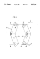
However, there were several disadvantages in the Clark-Lagerwall type liquid crystal display device. In its first model, it was presumed that the smectic-C phase has a layer structure named "bookshelf type" where layers lie vertical on a substrate as shown in FIG. 9. However, when a cell is created in accordance with a conventional orientation method such as rubbing and the like, the resultant switching phenomenon and optical characteristic are deviated from a prospective view a great deal, and it is observed that the practical switching operation is completely different from that in the proposed model.
As one of factors, the layer structure was analyzed using an X-ray small angle scattering method and it is found that the layer structure is that named "chevron" and having a dogleg shape [see Phys. Rev. Lett., 59, p. 2658 (1987) by T. P. Rieker, N. A. Clark et al.]. Another point different from the first model is reported that the cell assumes a twisted orientation where molecules are twisted in upper and lower substrates as well as a uniform orientation where the direction of the spontaneous polarization and liquid crystal molecules are oriented in a uniform direction [J. Phys. (France), 45, p. 143 (1984) by M. Glogarova and J. pavel].
Especially, a ferroelectric liquid crystal element having its orientation defined by rubbing has a strong adjusting force in its interface, and therefore, it is found that the element has a twisted orientation. With such an orientation, in general, no effective difference in optical molecule axis in switching between two states cannot be observed, and it is found that no high contrast characteristic can obtained. To eliminate such drawbacks, there have been presented several systems to attain a layer structure model first proposed by Clark et al., and one of them is reported that the model is created by SiO slanting vacuum evaporation, where with addition of a relatively high pre-tilt to a substrate interface, a layer structure having a tilt is attained without bends of layers.
As a second method, technology is proposed in which a layer structure is changed into a bookshelf structure by applying an alternating electric field of greater voltage to a cell with a bending structure [12th Liquid Crystal Discussion (in Nagoya) 1F16 (1986) by Satoh et al.], and according to the reports, both of the above two methods attained a high contrast characteristic. However, the above-mentioned slanting vacuum evaporation has a great problem in a stage of production that a technology of keeping a uniform deposition angle is not so simple and that the procedure includes a process performed under near vacuum. Moreover, as to a method of applying an electric field, it is difficult to uniformly change the layer structure, and many of preparation cells change back to chevron structure with time, and in other words, the method still stays in an experimental stage.
Accordingly, it is an object of the present invention to provide a liquid crystal display device of high contrast property despite its chevron structure.
SUMMARY OF THE INVENTION
The present invention provides a ferroelectric liquid crystal display device comprising:
upper and lower substrates arranged opposite to each other, each being provided with electrodes on their respective surface,
an insulating film formed on the electrodes on each of the substrates,
an orientation film formed on the insulating film and subjected to a uniaxial orientation treatment, the orientation film with the same orientation direction on each of the two substrates being oppositely arranged,
a liquid crystal composition with a chiral smectic C phase injected between the two substrates,
drive means for switching an optical axis of the liquid crystals in the liquid crystal composition by selectively applying a voltage to the electrodes,
means for optically identifying the switching of the optical axis,
in which when the drive means is operated, the liquid crystal composition can reverse its molecular direction near the substrate and show a chevron structure which bends in a dogleg shape as a layer structure when it shows the chiral smectic C phase wherein a bending direction of the dogleg shape is toward an inside of an area surrounded by a lightening defect produced by a direction of the uniaxial orientation treatment of the orientation film and a hairpin defect produced therebehind or an outside of an area surrounded by a hairpin defect produced by a direction of the uniaxial orientation treatment and a lightening defect produced therebehind, and a pretilt angle θp of the liquid crystal composition to the orientation film is between 8° and 35°.
Preferably, the orientation film is formed by an organic polymer film, and is formed through the uniaxial orientation treatment by rubbing.
BRIEF DESCRIPTION OF THE DRAWINGS
FIG. 1 is a sectional view showing a liquid crystal display device of an embodiment according to the present invention;
FIG. 2 is a schematic view showing a layer structure of a chiral smectic-C phase in the embodiment;
FIG. 3 is a schematic view showing C1 orientation and C2 orientation in the embodiment;
FIG. 4 is a diagram showing a rubbing treatment in the embodiment;
FIG. 5 is a diagram showing C-directors of C1 and C2 orientations in the embodiment;
FIG. 6 is a schematic view showing liquid crystal molecules in an interface of a substrate in the embodiment;
FIG. 7 is a schematic view showing a layer structure of a chiral smectic-C phase and an arrangement of the liquid crystal molecules in the embodiment;
FIG. 8 is a wave form diagram showing a bipolar pulse application state in the embodiment;
FIG. 9 is a schematic view showing a layer structure of a smectic-C phase in a conventional embodiment;
FIG. 10 is a schematic view showing another layer structure of a smectic-C phase in the conventional embodiment;
FIG. 11 is a graph showing relations between a rate of a memory angle θM to a tilt angle θ and the tilt angle θ in the embodiment of the liquid crystal display device according to the present invention and a comparison embodiment; and
FIG. 12 is a graph showing relations between a rate of a memory angle θM to a tilt angle θ and the tilt angle θ in another embodiment of the liquid crystal display device.
DESCRIPTION OF THE PREFERRED EMBODIMENTS
The present invention will be described in detail in conjunction with embodiments shown in the accompanying drawings. The present invention should not be limited to the description.
In general, it is known that a layer structure of a chiral smectic-C phase of a liquid crystal composition is a structure where layers bend in a dogleg shape. The cause of such a structure is that intervals among layers in a liquid crystal phase (generally, a smectic-A phase) on the side higher in temperature than the chiral smectic-C phase becomes smaller because liquid crystal molecules tilt when the liquid crystal phase varies to the chiral smectic-C phase while molecules near an interface of the substrate does not easily move to keep intervals among molecules in the phase on the side of higher temperature, and therefore, the layer intervals must be shortened without changing the molecule intervals in the interface, and the layers bend. However, the bends of the layers are caused in two directions (17, 18) as shown in FIG. 2, and this causes two different orientations. Then, orientation defects named zig-zag defects are caused in the position of the boundary between the layers bending in the different directions.
As shown in FIG. 2, two sorts of defects are found in the zig-zag defects depending upon the directions of the bends of the layers. Depending upon shapes, one of the defects, 15, is named lightning defects and the other 16 is named hairpin defects, and the direction of the bends of the layers can be assumed through the inspection of the shapes [Jpn. J. Appl. Phys., 28, p. 50 (1988)].
In the present invention, the bending structure is utilized, and the description about it will be discussed below. When the direction of the orientation treatment is the same in both the upper and lower substrates, there are two different orientation states depending upon whether the direction of the bends of the layers is the same as the direction of the orientation treatment or the former is reversed to the latter. The relations are shown in FIG. 3.
Circular cones shown in FIG. 3 represent orbits along which liquid crystal molecules move in switching, where liquid crystal tilts by tilt angle 26 related to a layer normal line 25. Arrow 19 denotes a direction of the rubbing. Regarding to the relations, as discussed in Japanese Unexamined Patent Publication 1-158415, a definition of a case where an axis of the rubbing and a direction of the bends of the layers are reversed to each other as shown in FIG. 3-23 is Chevron 1 (C1 orientation) while a definition of a case where the former and the latter are identical in direction as shown in FIG. 4-24 is Chevron 2 (C2 orientation). Like definitions designate the corresponding phenomena herein.
The C1 and C2 orientations show almost equivalent orientation states when there is made no pre-tilt of liquid crystal molecules in the substrate interface. However, when the single orientation treatment such as the rubbing treatment is performed, a pre-tilt angle 22 of the liquid crystal molecules is caused in the direction as shown in FIG. 4. As the pre-tilt is made greater, a difference in orientation state of the liquid crystal molecules between the C1 and C2 becomes gradually more conspicuous, and with the pre-tilt angle of 2° or more, the difference in orientation state becomes sufficiently conspicuous. The difference in orientation state is shown in FIG. 5.
Referring to FIGS. 5a, 5b and FIGS. 5c, 5d, states of molecules in memory states of the C1 and C2 orientations when the molecules in the substrate interface cannot easily move are illustrated with a presentation of C directors. The liquid crystal molecules are in a twisted state in the upper and lower substrates, and therefore, the C1 orientation in this case is defined as Chevron 1 Twist (C1Tw) orientation while the C2 orientation is defined as Chevron 2 Twist (C2Tw) orientation. The switching when an electric field is applied arises between "a" and "b", and "c" and "d". At this time, the switching in memory state arises only in a joint portion 14 of the chevron structure.
An arrangement of the molecules in the interfaces of the upper and lower substrates will be discussed referring to FIG. 3. An n director 20 makes a great twist in the C1Tw orientation while it makes a small twist in the C2Tw orientation. Assuming now that deflecting plates are disposed orthogonal to each other in upper and lower portions in a cell and the cell is rotated within them, there is no space for extinction in the C1Tw orientation while there is a space for extinction in the C2Tw orientation, and the C2Tw orientation can attain a better contrast characteristic, producing a darker display, than the C1Tw orientation (see Japanese Unexamined Patent Publication 1-158415). Meanwhile, allowing for the case where the molecules near the interface can move more easily and the interface reversal is consequently caused, the situation varies.
Referring to FIGS. 5e, 5f and FIGS. 5g, 5h, situations of molecules in memory states of the C1 and C2 orientations when the interface reversal is caused are illustrated. The twist of the liquid crystal molecules in the upper and lower substrates is untied, and therefore, the molecules are uniformly aligned. A definition of the C1 orientation in this case is Chevron 1 Uniform (C1U) orientation while a definition of the C2 orientation is Chevron 2 uniform (C2U) orientation. The switching when an electric field is applied arises between "e" and "f", and "g" and "h", respectively. In the C1U orientation in this situation, the twist of the molecules in the upper and lower substrate of the two memory states is untied. Moreover, since an angle of an optical axis between two memory states (memory angle θM) becomes larger, extinction in orthogonal nicols can be performed. In addition to that, when the optical axis is switched into the other memory state by setting a cell in an extinction point and applying voltage thereto, the optical axis angle moves a great deal, and therefore, a large light variation can be obtained. However, in the C2U orientation, even if the inversion of the molecules close to the interface is caused, a variation in the optical axis cannot be made a great deal between the first and second memory states as will be recognized in FIG. 5. Thus, it will be recognized that the C1U orientation brings about a higher contrast. Thus, with regard to the contrast characteristic, the following relations can be established: ##STR1##
While the C1U orientation is positively employed in this embodiment, especially in the case of the switching where the interface reversal such as a uniform orientation is utilized, the movement of the bulk of liquid crystal and the movement of the liquid crystal close to the interface are independent of each other; usually, a tendency is observed that the bulk of molecules can easily move while the molecules close to the interface do not easily move, and therefore, the switching with the interface reversal is liable to be very slow. However, it should be also possible that the switching of the inversion of the molecule in the substrate interface is performed a small voltage as possible and a narrow pulse width as possible depending upon the way of a control of the state of the interface.
FIG. 6 is a schematic diagram showing the liquid crystal molecules close to the substrate interface. In general, the liquid crystal molecules likely move with a variation in volume as small as possible against an electric field from the outside, and it is assumed that the molecules move on a cone-shaped orbit as shown in FIG. 6 to perform the switching without changing intervals of layers of the smectic-C. Thus, the molecules cannot make a perfect cone-shaped orbit because of an obstacle of the substrates near the substrate interfaces. Then, in the interface, a spontaneous polarization which the liquid crystal itself has is attracted or repulsed toward or from the substrate by an electric field 28 generated by a contact of the liquid crystal with the orientation film.
The liquid crystal molecules is laid under a constraint 31 of an anchor ring. Although the relation in force between them has not been clarified yet, the contact electric field and the constraint of the anchor ring can be reduced and the molecules take the cone-shaped orbit by keeping the molecules away from the substrates to cause the interface reversal more easily. Thus, it is found that the pre-tilt angle may be increased to cause the interface reversal phenomenon more easily. Experimentally, the reversal in the interface cannot be so often observed until the pre-tilt angle θP reaches 8° and above, but as the pre-tilt angle becomes larger, a switching time necessary for the interface reversal becomes shorter. However, as shown in FIG. 7, when the pre-tilt angle θP attains 35° and above, the direction of the normal line of the smectic layers comes to be perpendicular to the substrates, and accordingly, the orientation turns to the state where an ordinary switching cannot be performed. Thus, it is found that such a large pre-tilt angle is not good.
In the present invention, various liquid crystals are employed to find a corn angle (2θ) in the CIU orientation and a varied angle (memory angle θM) of the optical axis in the memory state, and it is recognized that they have relations with the pre-tilt angle θP made by the substrate and the liquid crystal molecules. Specifically, θM /2θ≈0.5 is satisfied when θP <θ while θM /2θ=1.0 is satisfied when θP >θ, or θM /2θ takes a value dispersed from 0.5 to 1.0 when θP ≈θ. Thus, selecting materials and the like so that the requirement θP ≧θ may be satisfied, an effective variation in the optical axis in the memory state can be attained, and a high contrast characteristic can be obtained.
Now described is a way how to distinguish an orientation state from the other. As to the distinguishing of the C1 from the C2, the direction of the bends of the layers can be assumed in accordance with the shapes of the zig-zag defects developed from spacers and flaws within the cell. Specifically, there are two sorts of shapes of the defects: a lightning type and a hairpin tupe. Usually, those two defects are connected to each other and closed, and the directions of the bends of the layers are different between an inside area surrounded by the defects and the outside (see FIG. 2), and thereby the direction of the rubbing and the direction of the bends of the layers can be assumed. The direction of the rubbing corresponds to the direction of the pre-tilt having the relations as shown in FIG. 4.
As to a discrimination method whether it is a twist orientation or a uniform orientation, there are judgment criterion according to the following two points:
1. When a microscopic observation is made to the cell to which a chopping wave is being applied, a reversed domain may be observed. At this time, a domain reversal (called "ship-shaped domain") caused by the shift of an internal disclination developed in a joint of a chevron is caused indifferent whether the cell assumes a twist orientation or a uniform orientation. Then, if one or more other domain reversal is observed beside the above-mentioned reversal, the reversal is a reversal in the interface, and it can be judged that the cell have experienced a uniform state in the switching.
2. This is the case where the optical axis angle between the two stable states (states where no voltage is applied) in the memory state is 40% or over of an angle of a displacement of the optical axis which is found by applying a sufficient electric field (approximately ±10 V) to the cell. In an ordinary twist orientation, a value at about 30% level can be barely attained.
EXAMPLE 1
FIG. 1 is a diagram showing a liquid crystal display device according to the present invention in section. Referring to FIG. 1, a plurality of transparent electrodes 2a having 300 to 5000 Å, or preferably, 1000 to 3000 Å thickness are disposed in stripes in parallel with each other on a glass substrate 1a. An electrode protecting film 3a of SiO2 having 300 to 5000 Å, or preferably 500 to 2000 Å thickness is formed by spattering upon them, and an orientation film 4a is formed further thereon by a spin coater. After that, a uniaxial orientation treatment through the rubbing where cloth of a rayon family is employed is practiced to form a substrate 9. On the other hand, in the similar conditions, a plurality of transparent electrodes 2b are disposed in stripes in parallel with each other on the other glass substrate 1b, and an orientation film 4b is formed through an electrode protecting film 3b upon them. After that, the uniaxial orientation treatment is practiced through the rubbing to form a substrate 10.
Then, the substrates 9 and 10 are stuck to each other by a seal 6 of epoxy resin via silica spacers 5 which makes intervals of 1.5 μm therebetween so that the respective orientation films 4a and 4b may be opposite to each other, the transparent electrodes 2a and 2b may be orthogonal to each other, and the rubbings may be almost identical in direction. A liquid crystal 7 (CS-1014 manufactured by Chisso Petrochemical Co., Ltd.) having a chiral smectic-C phase is heated and injected from an inlet between the substrates 9 and 10 according to a vacuum injection method, and thereafter the inlet is sealed by a UV hardened resin 8 to make a liquid crystal cell 11.
Furthermore, deflecting plates 12a and 12b are disposed orthogonal to a deflection axis in the top and bottom of the cell, and a deflection axis of one of the deflecting plates is almost aligned to one of optical axes of the liquid crystal of the cell to complete a liquid crystal display device. The orientation films 4a and 4b in the above mentioned embodiment includes nine kinds of orientation films having different values of the pre-tilt angle, thereby nine kinds of cells A to I are made. Another cell having about 20 μm thickness is made where the configuration is similar to the above and the directions of the rubbings are reversed but parallel to each other, and E-8 liquid crystal manufactured by Merk Company is injected. Then, the pre-tilt angle of liquid crystal molecules in the nematic phase is measured by a magnetic field capacity method. The liquid crystal different from the liquid crystal injected in the above is used because the liquid crystal having a chiral smectic-C phase has its molecules twisted in a cholesteric phase, and therefore, an accurate tilt angle cannot be measured.
Although it is generally known that a pre-tilt angle somewhat depends upon a liquid crystal material, most materials except special materials such as perfluoroalkyl develop pre-tilt angles with a dispersion of about 1 to 2, and hence, the substitute liquid crystal is used for the measurement. Table 1 below lists orientation films and respective measurements of pre-tilt angles.
              TABLE 1                                                     
______________________________________                                    
Cell No.                                                                  
        Orientation Films (Company)                                       
                             Pre-tilt Angle                               
______________________________________                                    
A       PSI-7355 (Chisso)    6                                            
B       PSI-7356 (Chisso)    6.5                                          
C       PSI-7354 (Chisso)    8                                            
D       LQ-1800 (Hitachi Chemical Ind.)                                   
                             8                                            
E       PSI-A-005 (Chisso)   13                                           
F       PSI-A-006 (Chisso)   13                                           
G       PSI-A-009 (Chisso)   15                                           
H       PSI-X-S130 (Chisso)  17                                           
I       RN-715 (Nissann Chemical)                                         
                             35                                           
______________________________________                                    
 Chisso: Chisso Petrochemical Co., Ltd.                                   
Then, a bipolar pulse of ±10 V 500 μsec as shown in FIG. 8 (the switching pulse has a pulse width approximately twice as fast as the switching speed (about 250 μsec) between the twist orientations, measured in the cell without an interface reversal) is applied to the cell to switch an optical axis so as to find in an area assuming the C1 orientation whether the switching arises between the uniform orientations. Table 2 below shows rates of the area assuming the C1U orientation and the results of the switching.
              TABLE 2                                                     
______________________________________                                    
A        X               10%                                              
B        X               10%                                              
C        X               30%                                              
D        Δ         35%                                              
E        O               90%                                              
F        O               90%                                              
G        O               95% or above                                     
H        O               95% or above                                     
I        X                0% (at 25° C.)                           
______________________________________                                    
 O The switching between the uniform orientations can be performed.       
 Δ Partially can be performed.                                      
 X The switching between the uniform orientations cannot be performed.    
As can be seen in Table 1, as the pre-tilt angle becomes large, especially as it reaches 8° and above, the switching can be performed. In a cell I where the pre-tilt angle attains 35° or above, the normal line of the smectic layer lies orthogonal to the substrates, the cell 1 assumes no C1 and C2 orientations at all and loses the switching function. When the pre-tilt is small, the cell easily assumes the C1Tw or C2 orientation, and it is recognized a great pre-tilt angle is effective in creating the C1U orientation.
In this way, the cells E, F, G and H can attain the C1U orientation over almost all the surface and are available for a quick switching. Moreover, two optical axes angles are made larger, and the contrast ratio between the two memory states can attain 40 or over.
EXAMPLE 2
A liquid crystal display device is manufactured in a configuration similar to the embodiment 1 (see FIG. 1). Ester mixed liquid crystals and pyrimidine mixed liquid crystals, which have a chiral smectic-C phase shown in Table 3, are mixed at rates shown in Table 4 into liquid crystal composites (2A to 2N in Table 4). As with the liquid crystals 2A to 2N, LC1 to BDH859 are mixed at rates in Table 4 (Table 4 reads 100 wt % from LC1 to BDH859), and thereafter, CH to TCNQ are added to the mixtures (amounts of the additive CH to TCNQ are represented in the rates to the total weight of the liquid crystals 2A to 2N).
These liquid crystal composites, while being heated, are injected from an inlet between the substrates 9 and 10 by a vacuum injection method, and then, the inlet is sealed by acrylic family UV hardened resin 8 to make a liquid crystal cell 11. Tilt angles of the liquid crystal composites are shown in Table 5.
                                  TABLE 3                                 
__________________________________________________________________________
LC1                                                                       
      ##STR2##                                                            
LC2                                                                       
      ##STR3##                                                            
LC3                                                                       
      ##STR4##                                                            
LC4                                                                       
      ##STR5##                                                            
LC5                                                                       
      ##STR6##                                                            
LC6                                                                       
      ##STR7##                                                            
LC7                                                                       
      ##STR8##                                                            
LC8                                                                       
      ##STR9##                                                            
LC9                                                                       
      ##STR10##                                                           
LC10                                                                      
      ##STR11##                                                           
LC11                                                                      
      ##STR12##                                                           
LC12                                                                      
      ##STR13##                                                           
LC13                                                                      
      ##STR14##                                                           
LC14                                                                      
      ##STR15##                                                           
LC15                                                                      
      ##STR16##                                                           
LC16                                                                      
      ##STR17##                                                           
LC17                                                                      
      ##STR18##                                                           
LC18                                                                      
      ##STR19##                     2M4: 2METHYLBUTHYL                    
LC19                                                                      
      ##STR20##                                                           
CH2                                                                       
      ##STR21##                                                           
CH1                                                                       
      ##STR22##                                                           
FA1                                                                       
      ##STR23##                                                           
TCNQ TETRACYANOQUINODIMETHANE                                             
BDH859                                                                    
     LIQUID CRYSTAL COMPOUNDS                                             
     (PRODUCT OF BDH Co.)                                                 
__________________________________________________________________________
                                  TABLE 4                                 
__________________________________________________________________________
Sheet 1                                                                   
  2A      2B 2C 2D 2E                                                       
                   2F  2G 2H                                              
                            2I 2J 2K  2L  2M 2N                           
__________________________________________________________________________
LC 1                      10                                              
LC 2                      5                                               
LC 3       15    15    15 17   15            15                           
LC 4       15    15    15 11   15            15                           
LC 5       25    25    25      25            25                           
LC 6       15    15    15 13   15            15                           
LC 7                      44                                              
LC 8       15    15    15      15            15                           
LC 9       10    10    10      10            10                           
LC 10      5      5    5       5             5                            
LC 11   15.3  15.3          15.3          15.3                            
LC 12   9.9   9.9           9.9           9.9                             
LC 13   15.1  15.1          15.1          15.1                            
LC 14   9.8   9.8           9.8           9.8                             
LC 15   1.49  1.49          1.49          1.49                            
LC 16   10    10            10            10                              
LC 17   9.8   9.8           9.8           9.8                             
LC 18   7.7   7.7           7.7           7.7                             
LC 19   7.5   7.5           7.5           7.5                             
BDH 859                                                                   
     100           100            100 100                                 
CH 1  2 0.2                                                               
           0.2                                                            
              2   2                                                       
                   0.2 0.2  2  2  0.2 2   0.2                             
                                             0.2                          
CH 2                      2                                               
FA 1       0.09                                                           
              0.09 0.09        0.09   0.09                                
                                          0.09                            
TCNQ    0.47  0.47 0.48                                                   
                       0.51    0.47                                       
(wt %)                                                                    
__________________________________________________________________________
              TABLE 5                                                     
______________________________________                                    
Liquid Crystal                                                            
            Tilt Angle θ                                            
                         Main Components                                  
______________________________________                                    
2A          22.3° Pyrimidine Mixed LC                              
2B          10.3° Ester Mixed LC                                   
2C          18.0° Pyrimidine Mixed LC                              
2D          12.7° Ester Mixed LC                                   
2E          18.1° Pyrimidine Mixed LC                              
2F          14.6° Pyrimidine Mixed LC                              
2G           7.1° Pyrimidine Mixed LC                              
2H          13.5° Pyrimidine Mixed LC                              
2I          14.1° Ester Mixed LC                                   
2J          14.5° Pyrimidine Mixed LC                              
2K          16.7° Pyrimidine Mixed LC                              
2L          22.4° Pyrimidine Mixed LC                              
2M          11.8° Ester Mixed LC                                   
2N           7.1° Pyrimidine Mixed LC                              
______________________________________                                    
Moreover, the deflecting panels 12a and 12b are disposed almost orthogonal to a deflecting axis in the top and bottom cells, and a deflecting axis of one of the deflecting panels is almost aligned to an optical axis of one of the liquid crystals of the cell to complete a liquid crystal display device. As the liquid crystal 7, as mentioned hereinafter, liquid crystals shown in 2B, 2D, 2F and 2G in Table 5 are those which satisfy the relation of pre-tilt angle θP ≧tilt angle θ, and are applied to the embodiments of the liquid crystal display device according to the present invention.
Another cell having about 20 μm thickness is made where the configuration is similar to the above and the directions of the rubbings are reversed but parallel to each other, and E-8 liquid crystal manufactured by Merk Company is injected. Then, the pre-tilt angle of liquid crystal molecules in the nematic phase is measured by a magnetic field capacity method. As a result, the pre-tilt angle θP is 12 to 15 in the orientation film PSI-A-2001. FIG. 11 is a graph in which the vertical axis shows a rate θM /2θ of a liquid crystal cone angle 2θ to a memory angle θM while the lateral axis shows the pre-tilt angle θP, and those factors about the liquid crystals 2A to 2G are plotted.
As can be seen in FIG. 11, when the cell assumes the C1U orientation, a value of θP >2θ when θP >θ with a boundary of θP ≈θ equals almost 1.0, and an effective optical axis angle can be obtained. However, it will be found that a value of θM /2θ when θP <θ is usually equal to about 0.5. In other words, in the liquid crystals 2G and 2B, θP >θ is satisfied and the memory angle θM corresponds to a value about twice as large as the tilt angle θ, while in the liquid crystals 2D and 2F, θP =θ is satisfied and the memory angle θM corresponds to a value about twice as large as the tilt angle θ, and thus, in either case, a value close to the optical axis angle (maximum optical axis angle) between the two states accomplished during the optimum switching operation can be obtained. On the contrary, in the liquid crystals 2A, 2C and 2E, θp<θ is satisfied, the memory angle θM merely takes a value almost equal to the tilt angle θ, and thus, merely a value close to almost the half of the optical axis angle between the two states accomplished during the optimum switching operation can be obtained.
Then, the case of θp <<θ will be described. Of the above mentioned components, PSI-XS-014 (polyimide amide) manufactured by Chisso Petrochemical Co., Ltd. is substituted for the orientation films 4a and 4b, and is similarly processed into a cell. Then, a plurality of liquid crystals (2I to 2N in Table 4) different in tilt angle are injected into the cell to make a liquid crystal cell.
Another cell having about 20 μm thickness is made where the configuration is similar to the above and the directions of the rubbings are reversed but parallel to each other, and E-8 liquid crystal manufactured by Merk Company is injected. Then, the pre-tilt angle of liquid crystal molecules in the nematic phase is measured by a magnetic field capacity method. As a result, the pre-tilt angle θp is 1° to 2° in the orientation film PSI-X-SO141. FIG. 12 is a graph in which the vertical axis shows a rate θM /2 θ of a liquid crystal cone angle 2θ to a memory angle θM in the case of the orientation film of PSI-X-S014 while the lateral axis shows the pre-tilt angle θp, and those factors about the liquid crystals 2I to 2N are plotted. In FIG. 12, the C1U orientation, C1Tw orientation, and C2Tw orientation are designated by O blots, x blots, and □ blots, respectively.
As can be seen in FIG. 12, when the cell assumes the C1U orientation, a value of θM /2θ when θp <<θ is equal merely to almost 0.5, and in other words, a value almost the half of the optical axis angle between the two states accomplished during the optimum switching operation can merely be obtained. While liquid crystals of the C1Tw orientation and C2Tw orientation in the event of θp <<θ are also plotted for reference, in this case, merely a value of θM /2 θ corresponds to almost 1/3, and it will be recognized that this is almost 35% of the optical axis angle between the two states accomplished during the optimum switching operation.
As the embodiment according to the present invention, an example where polyimide is employed with orientations of the liquid crystals 2B, 2D, 2F and 2G has been described, but other embodiments of various combinations of well-known liquid crystal materials, orientation film materials and orientation treatments can be in the scope of the present invention.
As has been described, in the liquid crystal display device according to the present invention, although it has a chevron structure, an optical axis angle between two states of liquid crystals during the switching operation can take a value almost close to the optical axis angle between the two states of the liquid crystal accomplished during the optimum switching operation, that is, it can take a value almost twice as large as a tilt angle of the liquid crystal. Thus, the switching operation which is a effective development of a feature of the liquid crystal can be implemented, and this is useful for providing a liquid crystal display device with a good contrast characteristic and for enhancing a utility of a ferroelectric liquid crystal display device. Moreover, setting a greater pre-tilt angle, an interface reversal phenomenon can be easily caused, and a switching time necessary for the interface reversal can be shortened.

Claims (4)

What is claimed is:
1. A ferroelectric liquid crystal device comprising:
upper and lower substrates, each being provided with electrodes on their respective surfaces, the substrates arranged with the electrode provided surfaces opposing each other
an insulating film formed on the electrodes on each of the substrates,
an orientation film formed on the insulating film and subjected to a uniaxial orientation treatment, the orientation film on each of the two substrates being arranged, wherein the orientation directions are the same,
a liquid crystal composition with a chiral smectic C phase injected between the two substrates,
drive means for switching an optical axis of the liquid crystals in the liquid crystal composition by selectively applying a voltage to the electrodes,
means for optically identifying the switching of the optical axis, in which when the drive means is operated, the liquid crystal composition can reverse its molecular direction near the substrate and show a chevron structure which bends in a dogleg shape as a layer structure when it shows the chiral smectic C phase wherein molecules of the liquid crystal composition that are arrayed in a field between a lightning defect and a hairpin defect appear to follow the lightning defect and to oppose a direction of the uniaxial orientation treatment and wherein a pretilt angle θp of the liquid crystal composition to the orientation film is between 8° and 35°.
2. A device according to claim 1, wherein the pretilt angle θp is equal to or over a tilt angle θ of a liquid crystal composition used.
3. A device according to claim 1 or 2, wherein said orientation film is an organic polymer film.
4. A device according to claim 1, wherein the uniaxial orientation treatment for the orientation film is rubbing.
US07823857 1991-01-25 1992-01-22 Ferroelectric liquid crystal display device with molecules between hairpin and lightning defects following the lightning defects Expired - Lifetime US5347381B1 (en)

Applications Claiming Priority (4)

Application Number Priority Date Filing Date Title
JP3-007879 1991-01-25
JP3007879A JP2880807B2 (en) 1991-01-25 1991-01-25 Liquid crystal display
JP3-032395 1991-01-31
JP3239591A JP2918343B2 (en) 1991-01-31 1991-01-31 Ferroelectric liquid crystal display

Publications (2)

Publication Number Publication Date
US5347381A true US5347381A (en) 1994-09-13
US5347381B1 US5347381B1 (en) 1997-07-01

Family

ID=26342264

Family Applications (1)

Application Number Title Priority Date Filing Date
US07823857 Expired - Lifetime US5347381B1 (en) 1991-01-25 1992-01-22 Ferroelectric liquid crystal display device with molecules between hairpin and lightning defects following the lightning defects

Country Status (4)

Country Link
US (1) US5347381B1 (en)
EP (1) EP0496628B1 (en)
KR (1) KR960011146B1 (en)
DE (1) DE69221646T2 (en)

Cited By (16)

* Cited by examiner, † Cited by third party
Publication number Priority date Publication date Assignee Title
US5404237A (en) * 1992-04-28 1995-04-04 Katsuse; Hirofumi Ferroelectric liquid crystal display having c2u alignment and the rewriting voltage<non-rewriting voltage
US5481387A (en) * 1990-03-02 1996-01-02 Canon Kabushiki Kaisha Chiral smectic liquid crystal element having uniform high temperature alignment and α≧8 degrees
US5557435A (en) * 1992-01-28 1996-09-17 Canon Kabushiki Kaisha Liquid crystal device and display apparatus
US5633740A (en) * 1993-05-10 1997-05-27 Canon Kabushiki Kaisha Chiral smectic liquid crystal device having at least one orientation film divided into regions with different uniaxial aligning treatment
US5644371A (en) * 1994-07-25 1997-07-01 Sharp Kabushiki Kaisha Liquid crystal display device and method for producing the same
US5646704A (en) * 1989-10-26 1997-07-08 Canon Kabushiki Kaisha Chiral smectic liquid crystal device having predetermined pre-tilt angle and intersection angle
US6083574A (en) * 1997-07-31 2000-07-04 Canon Kabushiki Kaisha Aligning method of liquid crystal, process for producing liquid crystal device, and liquid crystal device produced by the process
US6128064A (en) * 1999-07-14 2000-10-03 Canon Kabushiki Kaisha Liquid crystal device and liquid crystal display apparatus
US6195147B1 (en) 1997-08-01 2001-02-27 Canon Kabushiki Kaisha Liquid crystal substrate with optical modulation region having different alignment control forces
US6344840B1 (en) 1998-01-13 2002-02-05 Canon Kabushiki Kaisha Plasma-addressed liquid crystal display device
US6436490B1 (en) * 1999-04-30 2002-08-20 Sony Corporation Monostable ferroelectric liquid crystal display apparatus
US20030063057A1 (en) * 2001-09-28 2003-04-03 Akira Sakaigawa Liquid-crystal display device
US20040075082A1 (en) * 1999-08-31 2004-04-22 Canon Kabushiki Kaisha Single-crystalline film and process for production thereof
SG103908A1 (en) * 2002-04-09 2004-05-26 Toshiba Kk Apparatus and method for accessing a disk containing an alternate sector
US20050231803A1 (en) * 2003-10-17 2005-10-20 Handerek Vincent A Retroreflective devices and systems
CN112513699A (en) * 2018-08-02 2021-03-16 住友化学株式会社 Optical film

Families Citing this family (1)

* Cited by examiner, † Cited by third party
Publication number Priority date Publication date Assignee Title
GB9301051D0 (en) * 1993-01-20 1993-03-10 Marconi Gec Ltd Liquid crystal devices

Citations (13)

* Cited by examiner, † Cited by third party
Publication number Priority date Publication date Assignee Title
US4775225A (en) * 1985-05-16 1988-10-04 Canon Kabushiki Kaisha Liquid crystal device having pillar spacers with small base periphery width in direction perpendicular to orientation treatment
EP0307959A2 (en) * 1987-09-17 1989-03-22 Canon Kabushiki Kaisha Ferroelectric smectic liquid crystal device
US5005953A (en) * 1987-10-06 1991-04-09 Canon Kabushiki Kaisha High contrast liquid crystal element
EP0424944A2 (en) * 1989-10-26 1991-05-02 Canon Kabushiki Kaisha Ferroelectric liquid crystal device
EP0444705A2 (en) * 1990-03-02 1991-09-04 Canon Kabushiki Kaisha Liquid crystal element and liquid crystal apparatus using the same
US5046822A (en) * 1989-09-01 1991-09-10 Canon Kabushiki Kaisha Liquid crystal device
US5124827A (en) * 1990-01-31 1992-06-23 Stc Plc Ferroelectric liquid crystal cells
US5138473A (en) * 1987-07-20 1992-08-11 Commissariat A L'energie Atomique Ferroelectric liquid crystal screen with localized zigzag defects and opacified electrodes in the non-switchable area of the screen and processes for obtaining spacers and treating said screen
US5151804A (en) * 1989-06-12 1992-09-29 U.S. Philips Corporation Ferroelectric liquid crystal display having a spread of angles for grayscale and method of manufacture
US5164852A (en) * 1986-12-16 1992-11-17 Semiconductor Energy Laboratory Co., Ltd. Method of orientating a ferroelectric liquid crystal layer by AC electric field
US5182662A (en) * 1989-12-01 1993-01-26 Canon Kabushiki Kaisha Liquid crystal device
US5200848A (en) * 1987-09-17 1993-04-06 Canon Kabushiki Kaisha Ferroelectric smectic liquid crystal device
US5204766A (en) * 1991-03-28 1993-04-20 Canon Kabushiki Kaisha Ferroelectric liquid crystal cell with particulate adhesive density higher near side

Patent Citations (15)

* Cited by examiner, † Cited by third party
Publication number Priority date Publication date Assignee Title
US4775225A (en) * 1985-05-16 1988-10-04 Canon Kabushiki Kaisha Liquid crystal device having pillar spacers with small base periphery width in direction perpendicular to orientation treatment
US5164852A (en) * 1986-12-16 1992-11-17 Semiconductor Energy Laboratory Co., Ltd. Method of orientating a ferroelectric liquid crystal layer by AC electric field
US5138473A (en) * 1987-07-20 1992-08-11 Commissariat A L'energie Atomique Ferroelectric liquid crystal screen with localized zigzag defects and opacified electrodes in the non-switchable area of the screen and processes for obtaining spacers and treating said screen
EP0307959A2 (en) * 1987-09-17 1989-03-22 Canon Kabushiki Kaisha Ferroelectric smectic liquid crystal device
US4932758A (en) * 1987-09-17 1990-06-12 Canon Kabushiki Kaisha Ferroelectric smectic liquid crystal device having a bistable alignment state providing two stable orientation states
US5200848A (en) * 1987-09-17 1993-04-06 Canon Kabushiki Kaisha Ferroelectric smectic liquid crystal device
US5005953A (en) * 1987-10-06 1991-04-09 Canon Kabushiki Kaisha High contrast liquid crystal element
US5151804A (en) * 1989-06-12 1992-09-29 U.S. Philips Corporation Ferroelectric liquid crystal display having a spread of angles for grayscale and method of manufacture
US5046822A (en) * 1989-09-01 1991-09-10 Canon Kabushiki Kaisha Liquid crystal device
EP0424944A2 (en) * 1989-10-26 1991-05-02 Canon Kabushiki Kaisha Ferroelectric liquid crystal device
US5182662A (en) * 1989-12-01 1993-01-26 Canon Kabushiki Kaisha Liquid crystal device
US5124827A (en) * 1990-01-31 1992-06-23 Stc Plc Ferroelectric liquid crystal cells
EP0444705A2 (en) * 1990-03-02 1991-09-04 Canon Kabushiki Kaisha Liquid crystal element and liquid crystal apparatus using the same
US5189536A (en) * 1990-03-02 1993-02-23 Canon Kabushiki Kaisha Ferroelectric liquid crystal element having uniform high temperature alignment
US5204766A (en) * 1991-03-28 1993-04-20 Canon Kabushiki Kaisha Ferroelectric liquid crystal cell with particulate adhesive density higher near side

Non-Patent Citations (4)

* Cited by examiner, † Cited by third party
Title
Kanbe et al., "High Resolution, Large Area FLC Display With High Graphic Performance", Ferroelectrics, vol. 114, (1991), pp. 3-26.
Kanbe et al., High Resolution, Large Area FLC Display With High Graphic Performance , Ferroelectrics, vol. 114, (1991), pp. 3 26. *
Koden et al., "The States of Surface-Stabilized Ferrolectric Liquid Crystal With High-Pretilt Aligning Film", Japanese Journal of Applied Physics, vol. 30, No. 10B (Oct. 1991), pp. L1823-L1825.
Koden et al., The States of Surface Stabilized Ferrolectric Liquid Crystal With High Pretilt Aligning Film , Japanese Journal of Applied Physics, vol. 30, No. 10B (Oct. 1991), pp. L1823 L1825. *

Cited By (24)

* Cited by examiner, † Cited by third party
Publication number Priority date Publication date Assignee Title
US5646704A (en) * 1989-10-26 1997-07-08 Canon Kabushiki Kaisha Chiral smectic liquid crystal device having predetermined pre-tilt angle and intersection angle
US6456349B1 (en) 1990-03-02 2002-09-24 Canon Kabushiki Kaisha Liquid crystal element and liquid crystal apparatus using the same
US5481387A (en) * 1990-03-02 1996-01-02 Canon Kabushiki Kaisha Chiral smectic liquid crystal element having uniform high temperature alignment and α≧8 degrees
US5557435A (en) * 1992-01-28 1996-09-17 Canon Kabushiki Kaisha Liquid crystal device and display apparatus
US5404237A (en) * 1992-04-28 1995-04-04 Katsuse; Hirofumi Ferroelectric liquid crystal display having c2u alignment and the rewriting voltage<non-rewriting voltage
US5633740A (en) * 1993-05-10 1997-05-27 Canon Kabushiki Kaisha Chiral smectic liquid crystal device having at least one orientation film divided into regions with different uniaxial aligning treatment
US5644371A (en) * 1994-07-25 1997-07-01 Sharp Kabushiki Kaisha Liquid crystal display device and method for producing the same
US6083574A (en) * 1997-07-31 2000-07-04 Canon Kabushiki Kaisha Aligning method of liquid crystal, process for producing liquid crystal device, and liquid crystal device produced by the process
US6195147B1 (en) 1997-08-01 2001-02-27 Canon Kabushiki Kaisha Liquid crystal substrate with optical modulation region having different alignment control forces
US6344840B1 (en) 1998-01-13 2002-02-05 Canon Kabushiki Kaisha Plasma-addressed liquid crystal display device
US6573879B2 (en) 1998-01-13 2003-06-03 Canon Kabushiki Kaisha Plasma-addressed liquid crystal display device
US6436490B1 (en) * 1999-04-30 2002-08-20 Sony Corporation Monostable ferroelectric liquid crystal display apparatus
US6128064A (en) * 1999-07-14 2000-10-03 Canon Kabushiki Kaisha Liquid crystal device and liquid crystal display apparatus
US6982104B2 (en) 1999-08-31 2006-01-03 Canon Kabushiki Kaisha Single-crystalline film and process for production thereof
US20040075082A1 (en) * 1999-08-31 2004-04-22 Canon Kabushiki Kaisha Single-crystalline film and process for production thereof
US7153551B2 (en) 1999-08-31 2006-12-26 Canon Kabushiki Kaisha Single-crystalline film and process for production thereof
US6794533B1 (en) 1999-08-31 2004-09-21 Canon Kabushiki Kaisha Single-crystalline film and process for production thereof
US20060159863A1 (en) * 1999-08-31 2006-07-20 Canon Kabushiki Kaisha Single-crystalline film and process for production thereof
US20030063057A1 (en) * 2001-09-28 2003-04-03 Akira Sakaigawa Liquid-crystal display device
US6963322B2 (en) * 2001-09-28 2005-11-08 Sony Corporation Liquid-crystal display device
SG103908A1 (en) * 2002-04-09 2004-05-26 Toshiba Kk Apparatus and method for accessing a disk containing an alternate sector
US20050231803A1 (en) * 2003-10-17 2005-10-20 Handerek Vincent A Retroreflective devices and systems
CN112513699A (en) * 2018-08-02 2021-03-16 住友化学株式会社 Optical film
CN112513699B (en) * 2018-08-02 2022-09-13 住友化学株式会社 Optical film

Also Published As

Publication number Publication date
EP0496628B1 (en) 1997-08-20
EP0496628A2 (en) 1992-07-29
KR920015153A (en) 1992-08-26
DE69221646D1 (en) 1997-09-25
US5347381B1 (en) 1997-07-01
DE69221646T2 (en) 1998-03-12
KR960011146B1 (en) 1996-08-21
EP0496628A3 (en) 1992-12-23

Similar Documents

Publication Publication Date Title
US5347381A (en) Ferroelectric liquid crystal display device with molecules between hairpin and lightning defects following the lightning defects
JP2982330B2 (en) Liquid crystal display device
KR101100585B1 (en) Liquid crystal display device
US5790223A (en) Ferroelectric liquid crystal device and treatment method therefor
US6310677B1 (en) Liquid crystal device and liquid crystal display apparatus having a chevron structure in monostable alignment
EP0539991B1 (en) Liquid crystal device and display apparatus
US5646754A (en) Ferroelectric liquid crystal display device including a ferroelectric liquid crystal material capable of exhibiting the smectic A phase and the chiral smectic C phase
US5568295A (en) Chiral smetic LCD with small pretilt angle, substrate rubbed in two opposing directions, and no cholesteric phase or tilt angle &gt; the pretilt plus inclination angles
Oh-e et al. X-ray studies on layer structure and bistability in ferroelectric liquid crystals
US5523128A (en) Liquid crystal display device
US5537237A (en) Chiral smectic C liquid crystal display with a chevron structure and δθ equal to 0.9 to 1.0 at 25° C.
US5550664A (en) Liquid crystal display device
US5016989A (en) Liquid crystal element with improved contrast and brightness
US5956010A (en) Liquid crystal apparatus and driving method
JP2880807B2 (en) Liquid crystal display
JP2918343B2 (en) Ferroelectric liquid crystal display
JP3000504B2 (en) Liquid crystal element
US5726725A (en) Liquid crystal device and process for production thereof with polyimide alignment film rubbed and then baked
US5844653A (en) Liquid crystal mixture
Takatoh et al. Application of FLC/AFLC materials to active‐matrix devices
KR0161377B1 (en) Ferroelectric liquid crystal display element
JP2994854B2 (en) Liquid crystal composition and liquid crystal device using the same
JP3091091B2 (en) Liquid crystal display device
JPS6238421A (en) Liquid crystal display element
WO2011161663A1 (en) Liquid crystal display devices

Legal Events

Date Code Title Description
AS Assignment

Owner name: SHARP KABUSHIKI KAISHA A CORPORATION OF JAPAN

Free format text: ASSIGNMENT OF ASSIGNORS INTEREST.;ASSIGNORS:SHINOMIYA, TOKIHIKO;TANIGUCHI, TSUGIKO;KURATATE, TOMOAKI;AND OTHERS;REEL/FRAME:005992/0403

Effective date: 19920114

STCF Information on status: patent grant

Free format text: PATENTED CASE

FEPP Fee payment procedure

Free format text: PAYOR NUMBER ASSIGNED (ORIGINAL EVENT CODE: ASPN); ENTITY STATUS OF PATENT OWNER: LARGE ENTITY

B1 Reexamination certificate first reexamination
FPAY Fee payment

Year of fee payment: 4

DI Adverse decision in interference

Effective date: 20000414

DI Adverse decision in interference

Effective date: 20000414

DI Adverse decision in interference

Effective date: 20000414

FPAY Fee payment

Year of fee payment: 8

FPAY Fee payment

Year of fee payment: 12