US5345574A - Memory card having controller providing adjustable refresh to a plurality of DRAMs - Google Patents

Memory card having controller providing adjustable refresh to a plurality of DRAMs Download PDF

Info

Publication number
US5345574A
US5345574A US07/708,730 US70873091A US5345574A US 5345574 A US5345574 A US 5345574A US 70873091 A US70873091 A US 70873091A US 5345574 A US5345574 A US 5345574A
Authority
US
United States
Prior art keywords
refresh
random access
access memory
address
dynamic random
Prior art date
Legal status (The legal status is an assumption and is not a legal conclusion. Google has not performed a legal analysis and makes no representation as to the accuracy of the status listed.)
Expired - Lifetime
Application number
US07/708,730
Inventor
Noriaki Sakurada
Fujikazu Sugimoto
Ichiro Kobayashi
Current Assignee (The listed assignees may be inaccurate. Google has not performed a legal analysis and makes no representation or warranty as to the accuracy of the list.)
Seiko Epson Corp
Original Assignee
Seiko Epson Corp
Priority date (The priority date is an assumption and is not a legal conclusion. Google has not performed a legal analysis and makes no representation as to the accuracy of the date listed.)
Filing date
Publication date
Application filed by Seiko Epson Corp filed Critical Seiko Epson Corp
Assigned to SEIKO EPSON CORPORATION, A CORPORATION OF JAPAN reassignment SEIKO EPSON CORPORATION, A CORPORATION OF JAPAN ASSIGNMENT OF ASSIGNORS INTEREST. Assignors: KOBAYASHI, ICHIRO, SAKURADA, NORIAKI, SUGIMOTO, FUJIKAZU
Application granted granted Critical
Publication of US5345574A publication Critical patent/US5345574A/en
Anticipated expiration legal-status Critical
Expired - Lifetime legal-status Critical Current

Links

Images

Classifications

    • GPHYSICS
    • G11INFORMATION STORAGE
    • G11CSTATIC STORES
    • G11C11/00Digital stores characterised by the use of particular electric or magnetic storage elements; Storage elements therefor
    • G11C11/21Digital stores characterised by the use of particular electric or magnetic storage elements; Storage elements therefor using electric elements
    • G11C11/34Digital stores characterised by the use of particular electric or magnetic storage elements; Storage elements therefor using electric elements using semiconductor devices
    • G11C11/40Digital stores characterised by the use of particular electric or magnetic storage elements; Storage elements therefor using electric elements using semiconductor devices using transistors
    • G11C11/401Digital stores characterised by the use of particular electric or magnetic storage elements; Storage elements therefor using electric elements using semiconductor devices using transistors forming cells needing refreshing or charge regeneration, i.e. dynamic cells
    • G11C11/406Management or control of the refreshing or charge-regeneration cycles

Definitions

  • the invention relates generally to computer semiconductor memory cards based on dynamic random access memory (DRAM) devices and which consequently involve DRAM refresh operations, and in particular this invention relates to devices and methods that provide for refreshing of the DRAM devices on plug-in boards in an automatic way that is self-contained on the memory card and optimum for whatever type of DRAM devices are being used.
  • DRAM dynamic random access memory
  • DRAMs for main memory and for expansion board memory are conventional in personal computer systems.
  • DRAM-type memories need outside stimulus to "refresh" their individual memory cells periodically is well-known to those skilled in the art. See, “DRAM Refresh Modes," Motorola Semiconductor Application Note AN987, Motorola Memory Data, rev. 6, 1990, pp.13-2 to 13-3.
  • DRAMs have also traditionally only been offered in 16, 18, or 20-pin DIP packages and do not have enough pins to directly address the million or so bits of information inside. So the addresses have been traditionally multiplexed onto an address bus to reduce the number of address pins in the order of 50%. The outside interface to the DRAM must then split system addresses in half and send then along the same bus.
  • FIG. 10 illustrates a common prior art interfacing of a computer with DRAM.
  • a central processing unit (CPU) 100 sends a plurality of signals to a DRAM interface 101 which, in turn, modifies these signals and applies them to DRAM 102.
  • the CPU 100 signals include address 100a, read control (RD) 100b, write control (WR) 100c, memory request (MRQ) 100d, and refresh control (RFSH) 100e.
  • Databus 100f exchanges data bidirectionally and directly between CPU 100 and DRAM 102.
  • CPU 100 must issue periodic DRAM refresh cycles so that data at addresses within DRAM 102 do not spoil. Normal data transfers are suspended during such refresh cycles. The required period of refresh cycles depends on the actual type of DRAM device being employed in DRAM 102.
  • DRAM interface 101 provides row address strobe (RAS) 101a, column address strobe (CAS) 10lb, and multiplexed addresses 101c, 101d, and 101e.
  • DRAM interface circuit 101 outputs RAS 101a, CAS 10lb and address signals 101c, 101d and 101e, based on the particular states of address 100a and control signals RD 100b, WR 100c, and MRQ 100d.
  • RAS 101a, CAS 10lb and addresses 101c, 101d and 101e are periodically output in a sequence to DRAM 102 to retain data stored in the DRAM 102. (DRAM memory cells will be refreshed if simply addressed.)
  • FIG. 11 shows a generalized timing that is applicable to the circuit of FIG. 10.
  • CPU outputs address 100a, MRQ 100d goes low, and either RD 100b or WR 100c go low.
  • DRAM interface circuit 101 multiplexes the original address onto addresses 101c, 101d and 101e, and coordinates RAS 101a and CAS 10lb to indicate to DRAM 102 whether the address lines currently have the row or the column half of the complete address. (Note how the negative going edges of RAS 101a and CAS 10lb are skewed slightly in time.) Data is exchanged between CPU 100 (data to DRAM 102 if a write, data from DRAM 102 if a read cycle) over databus 100f with addresses in DRAM 102.
  • a refresh generator (e.g., a software program) is built into CPU 100 that outputs refresh signal (RFSH) 100e to DRAM interface circuit 101, along with an appropriate address signal 100a and MRQ 100d.
  • DRAM interface circuit 101 outputs RAS 101a, CAS 10l b, and address 101c, 101d and 101e in order to refresh DRAM 102 and thereby retain the data stored at the various addresses in DRAM 102.
  • the refresh operation need not be output by the CPU at completely arbitrary times. It is often preferable to output a refresh cycle at prescribed times, such as after fetching an instruction from memory.
  • Memory cards are a convenient way for users to add more memory to computer systems. Such cards can be plugged into sockets universally provided standard on most popular systems. Some of these prior art memory cards do not initiate their own refresh cycles. Such memory cards include only the equivalent function of DRAM 102.
  • the individual timing of refresh signals often differs, depending on the CPU being used. For practical reasons, no CPU can always supply an optimum refresh signal to every kind of DRAM-equipped memory card, because the needs of the DRAMs themselves differ, especially when comparing larger and smaller DRAMs.
  • Common refresh periods are 8, 16, 32, and 64 milliseconds. So if any of these four could be used, a prior art memory card would have to refresh every eight milliseconds to ensure that the memory is properly refreshed.
  • Other prior art systems always follow a read or write operation by a refresh operation, as a result, the overall access time of the memory card is stretched out.
  • a memory card is needed that can automatically refresh itself with an optimum refresh period, and one able to separate data transfers from refresh operations. Such a memory card would shorten access times and improve interoperability and reliability.
  • a memory card comprises means to generate RAS-before-CAS data access control signal timing and CAS-before-RAS refresh control signal timing, adjustable means to periodically request the means to generate to switch momentarily to refresh control timing, status indication means to inform the computer system a refresh cycle is in progress, a plurality of DRAM devices able to support CAS-before-RAS refresh cycles and in communication with the means to generate, and such that the periodic refresh request occurs at intervals optimum for the DRAM devices and is independent of any refresh requests generated by the computer system.
  • An advantage of the present invention is that a variety of DRAMs can be used, and whatever type is used can have the refresh period adjusted to suit its optimum interval.
  • FIG. 1 is a block diagram of a memory card, according to a first embodiment of the present invention
  • FIG. 2 is a timing chart of the various waveforms present at the first through the "n th " outputs of the counter in FIG. 1;
  • FIG. 3 is a block diagram of a memory card that is an example of a second embodiment of the present invention.
  • FIG. 4 is a timing chart showing the relationships between status register contents, card edge transfers, and DRAM access activity for the memory card of FIG. 3;
  • FIG. 5 is a block diagram of a memory card that is an example of a third embodiment of the present invention.
  • FIG. 6 is a timing chart showing the relationships between status register contents, card edge transfers, and DRAM access activity for the memory card of FIG. 5;
  • FIG. 7 is a block diagram of a memory card that is an example of a fourth embodiment of the present invention.
  • FIG. 8 is a timing chart showing the relationships between status register contents, card edge transfers, and DRAM access activity for the memory card of FIG. 7;
  • FIG. 9 is a timing chart showing access of a prior art DRAM by the CPU.
  • FIG. 10 is a block diagram of a memory card of the prior art.
  • FIG. 11 is a timing chart showing access of the DRAM by the CPU in FIG. 10.
  • FIG. 1 is a block diagram of a first embodiment memory card 14 of the present invention.
  • Memory card 14 comprises an oscillator 1, a counter 3, a selection means 4, a comparator 5 that outputs a refresh signal 6, a refresh controller 7, and a plurality of DRAMs 102.
  • the memory card 14 has self-generated refresh capability.
  • Oscillator 1 provides basic timing at a frequency "f o ".
  • a crystal oscillator set to 300 KHz has been found to be satisfactory. (Highly accurate 300 KHz crystals are inexpensive and widely available, they are used, for example in watches.)
  • the counter 3, selection means 4, and comparator 5 are able to produce selectable digital output periods of 8, 16, 32, and 64 milliseconds, using the oscillator 1 output as a reference.
  • Refresh controller 7 comprises the circuits necessary to initiate a burst refresh of all the row addresses in DRAMs 102 using CAS-before-RAS refresh cycles each 8, 16, 32, or 64 milliseconds.
  • DRAMs 102 for purposes of this discussion only, can be assumed to be 256K bit types organized as 64K by four bits. Twelve such devices will easily form into a memory array of 192K by 16.
  • Counter 3, containing individual flip-flops 2, together with selection means 4, comparator 5, and refresh controller 7 can, for example, all be integrated into a single ASIC chip that has an external crystal to support oscillator 1 and a number of external jumpers connected to option programming pins to support selection means 4.
  • Address 100a can be input to card 14 as a straight unmultiplexed 24 bit address, or it can be multiplexed in an I/O bus fashion on databus 100f.
  • a card enable signal 10 comprises, in an exemplary embodiment, a card enable, an output enable, a pair of card address signals, and a ready (RDY).
  • Read control 100b and write control 100c can be separate controls, as shown in FIG. 1, or can be reduced to a signal write enable (WE) used in conjunction with card enable (CE) and output enable (OE).
  • Refresh controller 7 must output CAS and RAS signals that follow normal RAS-before-CAS timing for data read/write and CAS-before-RAS timing to initiate each row refresh.
  • DRAMs such as type HM514256
  • write enable (WE) and output enable (OE) must also be output by controller 7 to DRAMs 102.
  • Addresses 100a are multiplexed by controller 7 onto the nine or more multiplexed addresses that must be input to DRAMs 102 that represent the column and row addresses. For such DRAM types, there will be 512 rows that need to be periodically refreshed.
  • DRAM Refresh Modes Motorola Semiconductor Application Note AN987, Motorola Memory Data, rev. 6, 1990, p.13-2.
  • FIG. 2 shows how the successive flip-flops 2 of counter 3 divide down the clock from oscillator 1. If the clock was 300 KHz to begin with, counter 3 must divide by 2400 to yield an output squarewave having a period of eight milliseconds. For a period of sixteen milliseconds, the division is 4800, and for 32 and 64 milliseconds, the divisions are 9600 and 19,200, respectively. As shown, the output "n" has a duty cycle of 50%. Refresh will occur only during the high level output. There will be 2400 ticks of the clock from oscillator 1 during this time, and a simple divide by four will provide 600 ticks per refresh burst period, or one tick every 13.3 microseconds.
  • FIG. 3 provides greater detail on the ASIC memory controller chip suggested above, it is referred to here as a second embodiment of the present invention.
  • DRAM 102 is equivalent to that described in the previous embodiment, and therefore uses the same element numbering.
  • Address 21 and databus 23 can be separate, as shown in FIG. 3, but I/O pins can be saved if, for example, a 24-bit address were multiplexed in three bytes over the databus 23 and held in addressable latches controlled by control input 22.
  • Control input 22 comprises RD, WR, and CE (read, write, and card enable). Additional chip or card address lines and a decoder can alternatively be added to support multiplexing the address 21 onto the databus 23.
  • Multiplexed nine-bit addresses are supplied to DRAMs 102 by data transfer control generator 24 working in conjunction with address MUX 25.
  • the addresses are timed to coincide with RAS and CAS and such coordination is conventional.
  • the refresh status of the memory controller can be determined by the CPU by addressing register 32 and by then inspecting a bit corresponding to signal 36.
  • data MUX 33 connects databus 23 to register 32.
  • the refresh of DRAM 102 is paced by oscillator 26.
  • Control MUX 28 will periodically shift front inputting normal RAS-before-CAS timed signals from data transfer control generator 24 to CAS-before-RAS timing from refresh control generator 27. How often refresh cycles are injected is controlled by counter 29, comparator 30, and refresh period adjustment means 31.
  • a refresh selection signal 36 will switch control MUX 28 every 8, 16, 32, or 64 milliseconds, for a duration of 4, 8, 16, or 32 milliseconds, respectively. Other durations and periods are possible, and may be preferable, and will depend in part on the particular types of devices being used for DRAMs 102.
  • FIG. 4 shows how a CPU can determine with a read of register 32 the refresh status to see if data is available (signal 36 low).
  • the status is unknown, several register read cycles 51 are made until the status returns an indication that a data read/write cycle is available. As soon as that happens, a window of opportunity opens up that will last for a predeterminable time duration, and the CPU can read data in a burst without further checking the refresh status. At the end of the opportunity, the CPU has to begin looping on the register status bit to wait for the next refresh cycle to finish.
  • Register read cycles 51 are repeated until the fact that data is again available is indicated by register 32.
  • the DRAM 102 cycles that correspond to the above are shown aligned in time with the card accesses by the external CPU.
  • Refresh operation cycles 61 are shown in burst mode.
  • refresh cycles 61 will just be equal in number to the number of rows in DRAM 102 and bursts will be spaced apart at near the maximum time allowed by the particular DRAM devices being used.
  • distributed, hidden, and write-with-CAS-before-RAS refresh timing can be used in the present invention.
  • FIG. 5 A third embodiment of the present invention is shown in FIG. 5 and is configured as a memory card similar to the first and second embodiments described above and in FIG. 3.
  • FIG. 6 is a corresponding timing chart, and is similar to FIG. 4.
  • FIG. 5 differs from FIG. 3 in that a delay module 38 has been added between comparator 30 and control MUX 28.
  • the effect of data transfer enable 36 on MUX 28 is skewed by delay 38. So even if the contents returned by register 32 are positive, control 34 will not be switched off until after a delay that effectively stretches the data transfer period. Immediately afterwards, refresh operations are executed automatically and the contents of register 32 will show the memory card to be ready for data transfers.
  • FIG. 7 is a block diagram of a fourth embodiment memory card.
  • FIG. 8 is a detailed block diagram of interface 71 (FIG. 7).
  • DRAM 102 is equivalent to the above embodiments.
  • An OSC 70 has a quartz crystal and outputs a fixed period clock.
  • An interface 71 controls DRAM 102 with address and control signals referenced to OSC 70 and a master external to the memory card.
  • a refresh requestor 71a divides the signal from OSC 70 and periodically outputs a refresh signal (REF) to initiate a refresh cycle in corresponding DRAM 102 on memory card 72.
  • a decoder 7lb outputs a RAS and a CAS based on the address, card enable (CE) and data transfer signals (WR, RD) from outside the memory card.
  • a dummy-cycle status indication 71c detects whether or not a RD signal together with a particular address signal from the external CPU are, in fact, indicating dummy-cycles (defined as reads of reserved, special addresses).
  • a refresh inhibitor 71d disables the RAS and CAS output from decoder 7lb from reaching DRAM 102 when a dummy-cycle is detected.
  • a refresh signal from refresh requestor 71a is based on dummy-cycle status indication signal detected by dummy-cycle detector 71c.
  • An address generator 71e generates a memory address based on REF signal, RAS and CAS output, without being inhibited by refresh inhibitor 71d and address signal from external CPU. The outputs of address generator 71e float (standby condition) during dummy-cycles because they are not needed by DRAM 102.
  • the external CPU outputs a dummy-cycle signal to interface 71 before accessing (data transfer) memory card 72.
  • detector 71c of interface 71 detects the dummy-cycle signal and signals refresh inhibitor 71d. Refresh requests from requestor 71a and RAS and CAS from decoder are disabled. The dummy-cycle causes address generator 71e to float its outputs.
  • interface 71 can do a data transfer with DRAM 102 after a fixed standby period has elapsed. Otherwise, a refresh request from refresh generator and RAS/CAS from decoder 7lb are output. DRAM 102 is thereby refreshed.
  • interface 71 gives precedence to refresh operation; i.e., any signal other than a dummy-cycle signal does not effect refresh operation.
  • An external CPU outputs a dummy signal to the interface circuit 40 of the memory card 41 before accessing (in a read or write data transfer operation) the memory card 41.
  • the dummy detection circuit 71c of the interface circuit 40 detects the dummy signal and the detected signal is input to the refresh inhibit circuit 71d, which immediately begins inhibiting the refresh signal generated from the refresh generation circuit 71a together with the RAS signal and CAS signal from the RAS, CAS generation circuit.
  • the address signal from the address generation circuit 71e goes to a floating condition.
  • the detection signal from the dummy detection circuit 71c is temporarily output to the refresh inhibit circuit 71d and address generation circuit 71e.
  • the interface circuit 71 executes read-write operation of the DRAM 102.
  • an oscillation source is included in the memory card and refresh operation is preformed automatically, and therefore no refresh signals need to be received from outside the memory card. Also, since the timing of the refresh signal need not be considered in the interface with main unit, when the memory card is used with the interface of a different unit, read-write operation is performed according to the read-write signal from the main unit while giving precedence to the refresh operation in the memory card, whereby a memory card with broad applicability is achieved.
  • the read-write period and refresh period are separated in the memory card and posted externally, and therefore the memory card need only be accessed during the read-write period, thus eliminating access during the refresh period and shortening the access time of the memory card. Also, since the memory card performs refresh operation by itself, a memory card with broad applicability to various models is achieved.
  • the memory card is temporarily set to a standby mode by the input of a dummy signal from outside the memory card, and read-write operation from outside the memory card or refresh operation by the memory card itself is performed after the standby condition has elapsed, whereby refresh operation by the memory card itself and read-write operation from outside the memory card are prevented from conflicting and the memory card can be accessed with greater efficiency.

Abstract

A dynamic access random access card is provided with a dynamic random access memory and a source for generating a plurality of reference clock pulses. A control circuit generates refresh operations of the dynamic access memory in response to the plurality of reference clock pulses generated by the source, the initiation of the refresh operations being independent of any external refresh request. The refresh operations are interrupted and the dynamic random access memory is set to a standby condition upon detection of a predetermined external signal, thereby permitting read/write operations of the dynamic random access memory.

Description

BACKGROUND OF THE INVENTION
The invention relates generally to computer semiconductor memory cards based on dynamic random access memory (DRAM) devices and which consequently involve DRAM refresh operations, and in particular this invention relates to devices and methods that provide for refreshing of the DRAM devices on plug-in boards in an automatic way that is self-contained on the memory card and optimum for whatever type of DRAM devices are being used.
The use of DRAMs for main memory and for expansion board memory is conventional in personal computer systems. The fact that DRAM-type memories need outside stimulus to "refresh" their individual memory cells periodically is well-known to those skilled in the art. See, "DRAM Refresh Modes," Motorola Semiconductor Application Note AN987, Motorola Memory Data, rev. 6, 1990, pp.13-2 to 13-3. DRAMs have also traditionally only been offered in 16, 18, or 20-pin DIP packages and do not have enough pins to directly address the million or so bits of information inside. So the addresses have been traditionally multiplexed onto an address bus to reduce the number of address pins in the order of 50%. The outside interface to the DRAM must then split system addresses in half and send then along the same bus. Half those addresses are strobed into DRAM registers with a "RAS" signal and the other half with a "CAS" signal. The RAS and CAS must be generated by the DRAM interface circuitry. But even though external DRAM interface and refresh circuitry typically adds cost and inserts refresh cycles that can interfere with and slow down system access, DRAM memories nevertheless compare very favorably with other types of devices on many different scores.
FIG. 10 illustrates a common prior art interfacing of a computer with DRAM. A central processing unit (CPU) 100 sends a plurality of signals to a DRAM interface 101 which, in turn, modifies these signals and applies them to DRAM 102. The CPU 100 signals include address 100a, read control (RD) 100b, write control (WR) 100c, memory request (MRQ) 100d, and refresh control (RFSH) 100e. Databus 100f exchanges data bidirectionally and directly between CPU 100 and DRAM 102. CPU 100 must issue periodic DRAM refresh cycles so that data at addresses within DRAM 102 do not spoil. Normal data transfers are suspended during such refresh cycles. The required period of refresh cycles depends on the actual type of DRAM device being employed in DRAM 102.
DRAM interface 101 provides row address strobe (RAS) 101a, column address strobe (CAS) 10lb, and multiplexed addresses 101c, 101d, and 101e. DRAM interface circuit 101 outputs RAS 101a, CAS 10lb and address signals 101c, 101d and 101e, based on the particular states of address 100a and control signals RD 100b, WR 100c, and MRQ 100d. (The control signals are all low true, as is the custom in such designs, but the signal names are not shown as RD, WR, MRQ, etc., for the sake of simplicity.) During refresh operations, RAS 101a, CAS 10lb and addresses 101c, 101d and 101e are periodically output in a sequence to DRAM 102 to retain data stored in the DRAM 102. (DRAM memory cells will be refreshed if simply addressed.)
FIG. 11 shows a generalized timing that is applicable to the circuit of FIG. 10. To access DRAM 102, CPU outputs address 100a, MRQ 100d goes low, and either RD 100b or WR 100c go low. DRAM interface circuit 101 multiplexes the original address onto addresses 101c, 101d and 101e, and coordinates RAS 101a and CAS 10lb to indicate to DRAM 102 whether the address lines currently have the row or the column half of the complete address. (Note how the negative going edges of RAS 101a and CAS 10lb are skewed slightly in time.) Data is exchanged between CPU 100 (data to DRAM 102 if a write, data from DRAM 102 if a read cycle) over databus 100f with addresses in DRAM 102. A refresh generator (e.g., a software program) is built into CPU 100 that outputs refresh signal (RFSH) 100e to DRAM interface circuit 101, along with an appropriate address signal 100a and MRQ 100d. DRAM interface circuit 101 outputs RAS 101a, CAS 10l b, and address 101c, 101d and 101e in order to refresh DRAM 102 and thereby retain the data stored at the various addresses in DRAM 102. The refresh operation need not be output by the CPU at completely arbitrary times. It is often preferable to output a refresh cycle at prescribed times, such as after fetching an instruction from memory.
Memory cards are a convenient way for users to add more memory to computer systems. Such cards can be plugged into sockets universally provided standard on most popular systems. Some of these prior art memory cards do not initiate their own refresh cycles. Such memory cards include only the equivalent function of DRAM 102. The individual timing of refresh signals often differs, depending on the CPU being used. For practical reasons, no CPU can always supply an optimum refresh signal to every kind of DRAM-equipped memory card, because the needs of the DRAMs themselves differ, especially when comparing larger and smaller DRAMs. Common refresh periods are 8, 16, 32, and 64 milliseconds. So if any of these four could be used, a prior art memory card would have to refresh every eight milliseconds to ensure that the memory is properly refreshed. Other prior art systems always follow a read or write operation by a refresh operation, as a result, the overall access time of the memory card is stretched out.
A memory card is needed that can automatically refresh itself with an optimum refresh period, and one able to separate data transfers from refresh operations. Such a memory card would shorten access times and improve interoperability and reliability.
SUMMARY OF THE INVENTION
According to the present invention, a memory card comprises means to generate RAS-before-CAS data access control signal timing and CAS-before-RAS refresh control signal timing, adjustable means to periodically request the means to generate to switch momentarily to refresh control timing, status indication means to inform the computer system a refresh cycle is in progress, a plurality of DRAM devices able to support CAS-before-RAS refresh cycles and in communication with the means to generate, and such that the periodic refresh request occurs at intervals optimum for the DRAM devices and is independent of any refresh requests generated by the computer system.
An advantage of the present invention is that a variety of DRAMs can be used, and whatever type is used can have the refresh period adjusted to suit its optimum interval.
Other objects and attainments together with a fuller understanding of the invention will become apparent and appreciated to those skilled in the art by referring to the following description and claims taken in conjunction with the accompanying drawings.
BRIEF DESCRIPTION OF THE DRAWINGS
FIG. 1 is a block diagram of a memory card, according to a first embodiment of the present invention;
FIG. 2 is a timing chart of the various waveforms present at the first through the "nth " outputs of the counter in FIG. 1;
FIG. 3 is a block diagram of a memory card that is an example of a second embodiment of the present invention;
FIG. 4 is a timing chart showing the relationships between status register contents, card edge transfers, and DRAM access activity for the memory card of FIG. 3;
FIG. 5 is a block diagram of a memory card that is an example of a third embodiment of the present invention;
FIG. 6 is a timing chart showing the relationships between status register contents, card edge transfers, and DRAM access activity for the memory card of FIG. 5;
FIG. 7 is a block diagram of a memory card that is an example of a fourth embodiment of the present invention;
FIG. 8 is a timing chart showing the relationships between status register contents, card edge transfers, and DRAM access activity for the memory card of FIG. 7;
FIG. 9 is a timing chart showing access of a prior art DRAM by the CPU;
FIG. 10 is a block diagram of a memory card of the prior art; and
FIG. 11 is a timing chart showing access of the DRAM by the CPU in FIG. 10.
DESCRIPTION OF THE PREFERRED EMBODIMENTS
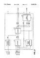
FIG. 1 is a block diagram of a first embodiment memory card 14 of the present invention. Memory card 14 comprises an oscillator 1, a counter 3, a selection means 4, a comparator 5 that outputs a refresh signal 6, a refresh controller 7, and a plurality of DRAMs 102. The memory card 14 has self-generated refresh capability. Oscillator 1 provides basic timing at a frequency "fo ". A crystal oscillator set to 300 KHz has been found to be satisfactory. (Highly accurate 300 KHz crystals are inexpensive and widely available, they are used, for example in watches.) The counter 3, selection means 4, and comparator 5 are able to produce selectable digital output periods of 8, 16, 32, and 64 milliseconds, using the oscillator 1 output as a reference. Other selectable periods could be used, but these periods match the most common refresh periods of the popular DRAM chips currently available. Refresh controller 7 comprises the circuits necessary to initiate a burst refresh of all the row addresses in DRAMs 102 using CAS-before-RAS refresh cycles each 8, 16, 32, or 64 milliseconds. DRAMs 102, for purposes of this discussion only, can be assumed to be 256K bit types organized as 64K by four bits. Twelve such devices will easily form into a memory array of 192K by 16. Counter 3, containing individual flip-flops 2, together with selection means 4, comparator 5, and refresh controller 7 can, for example, all be integrated into a single ASIC chip that has an external crystal to support oscillator 1 and a number of external jumpers connected to option programming pins to support selection means 4. Address 100a can be input to card 14 as a straight unmultiplexed 24 bit address, or it can be multiplexed in an I/O bus fashion on databus 100f. A card enable signal 10 comprises, in an exemplary embodiment, a card enable, an output enable, a pair of card address signals, and a ready (RDY). Read control 100b and write control 100c can be separate controls, as shown in FIG. 1, or can be reduced to a signal write enable (WE) used in conjunction with card enable (CE) and output enable (OE). Refresh controller 7 must output CAS and RAS signals that follow normal RAS-before-CAS timing for data read/write and CAS-before-RAS timing to initiate each row refresh. If DRAMs, such as type HM514256 are used, write enable (WE) and output enable (OE) must also be output by controller 7 to DRAMs 102. Addresses 100a are multiplexed by controller 7 onto the nine or more multiplexed addresses that must be input to DRAMs 102 that represent the column and row addresses. For such DRAM types, there will be 512 rows that need to be periodically refreshed.
The refresh of DRAMs 102 can be done in either a single burst of 512 consecutive refresh cycles (one cycle per row) every 8, 16, 32, or 64 milliseconds, or distributed over time (e,g., eight milliseconds over 512 rows=15.6 microseconds per row), or some combination of these two extremes. ("DRAM Refresh Modes," Motorola Semiconductor Application Note AN987, Motorola Memory Data, rev. 6, 1990, p.13-2.)
FIG. 2 shows how the successive flip-flops 2 of counter 3 divide down the clock from oscillator 1. If the clock was 300 KHz to begin with, counter 3 must divide by 2400 to yield an output squarewave having a period of eight milliseconds. For a period of sixteen milliseconds, the division is 4800, and for 32 and 64 milliseconds, the divisions are 9600 and 19,200, respectively. As shown, the output "n" has a duty cycle of 50%. Refresh will occur only during the high level output. There will be 2400 ticks of the clock from oscillator 1 during this time, and a simple divide by four will provide 600 ticks per refresh burst period, or one tick every 13.3 microseconds. Since 512 rows are contained in a typical DRAM 102, then 600 will be more than enough cycles in a burst to guarantee that all rows are refreshed in an eight millisecond period. While the output "n" of counter 3 is high, signal 6 will be high, and memory card 14 will not be available for data read/writes since it is busy with refresh. By changing counter 3, selection means 4, and comparator 5, a refresh signal 6 can be produced that has a duty cycle less that 50%, and thus will make memory card 14 more available for data transfers.
FIG. 3 provides greater detail on the ASIC memory controller chip suggested above, it is referred to here as a second embodiment of the present invention. DRAM 102 is equivalent to that described in the previous embodiment, and therefore uses the same element numbering. Address 21 and databus 23 can be separate, as shown in FIG. 3, but I/O pins can be saved if, for example, a 24-bit address were multiplexed in three bytes over the databus 23 and held in addressable latches controlled by control input 22. Control input 22 comprises RD, WR, and CE (read, write, and card enable). Additional chip or card address lines and a decoder can alternatively be added to support multiplexing the address 21 onto the databus 23. Multiplexed nine-bit addresses (typical) are supplied to DRAMs 102 by data transfer control generator 24 working in conjunction with address MUX 25. The addresses are timed to coincide with RAS and CAS and such coordination is conventional. The refresh status of the memory controller can be determined by the CPU by addressing register 32 and by then inspecting a bit corresponding to signal 36. When register 32 is properly addressed, data MUX 33 connects databus 23 to register 32. The refresh of DRAM 102 is paced by oscillator 26. Control MUX 28 will periodically shift front inputting normal RAS-before-CAS timed signals from data transfer control generator 24 to CAS-before-RAS timing from refresh control generator 27. How often refresh cycles are injected is controlled by counter 29, comparator 30, and refresh period adjustment means 31. The overall function and purpose is described above in conjunction with counter 3, selection means 4, and comparator 5. A refresh selection signal 36 will switch control MUX 28 every 8, 16, 32, or 64 milliseconds, for a duration of 4, 8, 16, or 32 milliseconds, respectively. Other durations and periods are possible, and may be preferable, and will depend in part on the particular types of devices being used for DRAMs 102.
FIG. 4 shows how a CPU can determine with a read of register 32 the refresh status to see if data is available (signal 36 low). When the status is unknown, several register read cycles 51 are made until the status returns an indication that a data read/write cycle is available. As soon as that happens, a window of opportunity opens up that will last for a predeterminable time duration, and the CPU can read data in a burst without further checking the refresh status. At the end of the opportunity, the CPU has to begin looping on the register status bit to wait for the next refresh cycle to finish. Register read cycles 51 are repeated until the fact that data is again available is indicated by register 32. The DRAM 102 cycles that correspond to the above are shown aligned in time with the card accesses by the external CPU. Refresh operation cycles 61 are shown in burst mode. Preferably, refresh cycles 61 will just be equal in number to the number of rows in DRAM 102 and bursts will be spaced apart at near the maximum time allowed by the particular DRAM devices being used. Alternatively, distributed, hidden, and write-with-CAS-before-RAS refresh timing can be used in the present invention.
A third embodiment of the present invention is shown in FIG. 5 and is configured as a memory card similar to the first and second embodiments described above and in FIG. 3. FIG. 6 is a corresponding timing chart, and is similar to FIG. 4. FIG. 5 differs from FIG. 3 in that a delay module 38 has been added between comparator 30 and control MUX 28. The effect of data transfer enable 36 on MUX 28 is skewed by delay 38. So even if the contents returned by register 32 are positive, control 34 will not be switched off until after a delay that effectively stretches the data transfer period. Immediately afterwards, refresh operations are executed automatically and the contents of register 32 will show the memory card to be ready for data transfers.
FIG. 7 is a block diagram of a fourth embodiment memory card. FIG. 8 is a detailed block diagram of interface 71 (FIG. 7). DRAM 102 is equivalent to the above embodiments. An OSC 70 has a quartz crystal and outputs a fixed period clock. An interface 71 controls DRAM 102 with address and control signals referenced to OSC 70 and a master external to the memory card. A refresh requestor 71a divides the signal from OSC 70 and periodically outputs a refresh signal (REF) to initiate a refresh cycle in corresponding DRAM 102 on memory card 72. A decoder 7lb outputs a RAS and a CAS based on the address, card enable (CE) and data transfer signals (WR, RD) from outside the memory card. A dummy-cycle status indication 71c detects whether or not a RD signal together with a particular address signal from the external CPU are, in fact, indicating dummy-cycles (defined as reads of reserved, special addresses). A refresh inhibitor 71d disables the RAS and CAS output from decoder 7lb from reaching DRAM 102 when a dummy-cycle is detected. A refresh signal from refresh requestor 71a is based on dummy-cycle status indication signal detected by dummy-cycle detector 71c. An address generator 71e generates a memory address based on REF signal, RAS and CAS output, without being inhibited by refresh inhibitor 71d and address signal from external CPU. The outputs of address generator 71e float (standby condition) during dummy-cycles because they are not needed by DRAM 102.
In FIG. 7, the external CPU outputs a dummy-cycle signal to interface 71 before accessing (data transfer) memory card 72. So detector 71c of interface 71 detects the dummy-cycle signal and signals refresh inhibitor 71d. Refresh requests from requestor 71a and RAS and CAS from decoder are disabled. The dummy-cycle causes address generator 71e to float its outputs. When CE signal 42 and either RD 100b or WR 100c are received from external CPU, interface 71 can do a data transfer with DRAM 102 after a fixed standby period has elapsed. Otherwise, a refresh request from refresh generator and RAS/CAS from decoder 7lb are output. DRAM 102 is thereby refreshed. When CE signal 42, address signal and RD 100b, or CE signal 42, address signal and WR 100c from external CPU are input to interface 71 during refresh operation, then interface 71 gives precedence to refresh operation; i.e., any signal other than a dummy-cycle signal does not effect refresh operation. An external CPU outputs a dummy signal to the interface circuit 40 of the memory card 41 before accessing (in a read or write data transfer operation) the memory card 41. The dummy detection circuit 71c of the interface circuit 40 detects the dummy signal and the detected signal is input to the refresh inhibit circuit 71d, which immediately begins inhibiting the refresh signal generated from the refresh generation circuit 71a together with the RAS signal and CAS signal from the RAS, CAS generation circuit. When the detection signal from the dummy detection circuit 71c is input to the address generation circuit 71e, the address signal from the address generation circuit 71e goes to a floating condition. The detection signal from the dummy detection circuit 71c is temporarily output to the refresh inhibit circuit 71d and address generation circuit 71e. When the CE signal 42 and RD signal 100b or WR signal 100c from the external CPU are input to the interface circuit 71 after a fixed period in the standby condition has elapsed, then the interface circuit 71 executes read-write operation of the DRAM 102. When the CE signal 42, address signal and RD signal 100b, or CE signal 42, address signal and WR signal 100c from the external CPU are not input, then the refresh signal from the refresh generation circuit and the RAS signal and CAS signal from the RAS, CAS generation circuit 7lb are output to the DRAM 102 and the DRAM 102 is refreshed. When the CE signal 42, address signal and RD signal 100b, or CE signal 42, address signal and WR signal 100c from the external CPU are input to the interface circuit 71 during refresh operation, then the interface circuit 71 gives precedence to the refresh operation; i.e., any signal other than a dummy signal does not effect refresh operation.
As described above, by means of the invention, an oscillation source is included in the memory card and refresh operation is preformed automatically, and therefore no refresh signals need to be received from outside the memory card. Also, since the timing of the refresh signal need not be considered in the interface with main unit, when the memory card is used with the interface of a different unit, read-write operation is performed according to the read-write signal from the main unit while giving precedence to the refresh operation in the memory card, whereby a memory card with broad applicability is achieved.
In addition, the read-write period and refresh period are separated in the memory card and posted externally, and therefore the memory card need only be accessed during the read-write period, thus eliminating access during the refresh period and shortening the access time of the memory card. Also, since the memory card performs refresh operation by itself, a memory card with broad applicability to various models is achieved.
Further, by delaying the read-write period in the memory card so it extends into the refresh period, read-write operation can be performed during that delay time, thus increasing the utility of the memory card.
The memory card is temporarily set to a standby mode by the input of a dummy signal from outside the memory card, and read-write operation from outside the memory card or refresh operation by the memory card itself is performed after the standby condition has elapsed, whereby refresh operation by the memory card itself and read-write operation from outside the memory card are prevented from conflicting and the memory card can be accessed with greater efficiency.
While present invention has been described in conjunction with several specific embodiments, it is evident to those skilled in art that many further alternatives, modifications and variations will be apparent in light of forgoing description. Thus, present invention described herein is intended to embrace all such alternatives, modifications, applications and variations that may fall within spirit and scope of appended claims.

Claims (6)

What is claimed is:
1. A memory card comprising:
means for generating a reference clock having a predetermined reference clock period;
a dynamic random access memory;
refresh generation means for automatically initiating periodic refresh operations of said dynamic random access memory at a predetermined frequency independent of any externally applied refresh requests, the automatic initiation commencing each integer number "n" of the predetermined reference clock period;
means for generating dynamic random access memory row-address-strobe-before-column-address-strobe timing signals and multiplexed addresses in response to address and control signals indicating data transfer requests from an external central processing unit, wherein the means for generating dynamic random access memory row-address-strobe-before-column-address-strobe timing and multiplexed addresses comprises a first multiplexer for generating the multiplexed addresses;
means for selecting the integer number "n" such that the predetermined frequency of the dynamic random access memory refresh operations by said refresh generation means is adjustable,
wherein the refresh generation means comprises a counter for counting a number of pulses of the reference clock, a comparison means for comparing the counted number of pulses to the integer number "n" received from the means for selecting, and a second multiplexer for switching said dynamic random access memory between row-address-strobe-before-column-address-strobe timing and column-address-strobe-before-row-address-strobe timing when the count of the pulses counted by said counter is equal to the number "n"; and
status indication means for indicating to the external central process unit when said refresh generation means is refreshing said dynamic random access memory.
2. The memory card of claim 1, wherein
said refresh generation means further comprises means for setting a status bit indicating that said refresh generation means is refreshing said dynamic random access memory; and
wherein said status indication means provides the indication to the external CPU in response to the status bit set by said refresh generation means.
3. The memory card of claim 2, further comprising:
delay means for inserting a delay switching of said second multiplexer such that a time available for data transfer operations is extended.
4. The memory card of claim 1, wherein said status indication means comprising a third multiplexer so that the external central processing unit selectively performs one of reading/writing data to said dynamic random access memory and reading an indication from said status indication means.
5. A dynamic random access memory card comprising:
dynamic random access memory requiring periodic refreshing to maintain stored data therein; and
an application specific integrated circuit dynamic random access memory controller comprising,
an input/output bus port for selectively inputting data to said dynamic random access memory from an external central processing unit and for outputting data from said dynamic random access memory to the external central processing unit,
a multiplexed address output port and coordinated row-address-strobe and column-address-strobe controls for interfacing with said dynamic random access memory,
an oscillator means for generating a clock signal,
means for burst refreshing said dynamic random access memory with column-address-strobe-before-row-address-strobe control timing signals at a predetermined frequency in accordance the clock signal generated by said oscillator means,
means for externally adjusting the predetermined frequency of the burst refreshing by said means for burst refreshing, and
means for providing a status of the burst refreshing of said dynamic random access memory by said means for burst refreshing to the external central processing unit, wherein:
the clock signal generated by said oscillator means has a frequency of about 300 KHz; and
the predetermined frequency of burst refresh cycles adjusted by said means for adjusting is selectable from one of 8, 16, 32, and 64 milliseconds.
6. The dynamic random access memory card of claim 5, wherein said oscillator means comprises a crystal-controlled oscillator having connections for a crystal arranged externally to said memory controller.
US07/708,730 1990-05-15 1991-05-15 Memory card having controller providing adjustable refresh to a plurality of DRAMs Expired - Lifetime US5345574A (en)

Applications Claiming Priority (10)

Application Number Priority Date Filing Date Title
JP12475390 1990-05-15
JP12614390 1990-05-16
JP13322390 1990-05-23
JP2-138974 1990-05-29
JP2-124753 1990-05-29
JP2-126143 1990-05-29
JP13897490 1990-05-29
JP2-133223 1990-05-29
JP3-80169 1991-04-12
JP08016991A JP3225531B2 (en) 1990-05-15 1991-04-12 Memory card

Publications (1)

Publication Number Publication Date
US5345574A true US5345574A (en) 1994-09-06

Family

ID=27524848

Family Applications (1)

Application Number Title Priority Date Filing Date
US07/708,730 Expired - Lifetime US5345574A (en) 1990-05-15 1991-05-15 Memory card having controller providing adjustable refresh to a plurality of DRAMs

Country Status (2)

Country Link
US (1) US5345574A (en)
JP (1) JP3225531B2 (en)

Cited By (22)

* Cited by examiner, † Cited by third party
Publication number Priority date Publication date Assignee Title
US5446695A (en) * 1994-03-22 1995-08-29 International Business Machines Corporation Memory device with programmable self-refreshing and testing methods therefore
US5557577A (en) * 1995-05-01 1996-09-17 Apple Computer, Inc. System and method for performing wake-up operations to a memory
US5557578A (en) * 1995-05-01 1996-09-17 Apple Computer, Inc. Dynamic memory refresh controller and method
US5613094A (en) * 1994-10-17 1997-03-18 Smart Modular Technologies Method and apparatus for enabling an assembly of non-standard memory components to emulate a standard memory module
US5638529A (en) * 1992-08-24 1997-06-10 Intel Corporation Variable refresh intervals for system devices including setting the refresh interval to zero
US5643533A (en) * 1995-05-12 1997-07-01 Fishman; Yoram Method of packaged goods sterilization
US5689677A (en) * 1995-06-05 1997-11-18 Macmillan; David C. Circuit for enhancing performance of a computer for personal use
US5796668A (en) * 1995-09-06 1998-08-18 Samsung Electronics Co., Ltd. Integrated circuit memory devices having reduced write cycle times and related methods
US5822753A (en) * 1992-10-01 1998-10-13 Hudson Soft Co., Ltd. Information processing system with a memory control unit for refreshing a memory
US5881314A (en) * 1995-10-30 1999-03-09 Samsung Electronics Co., Ltd. Memory control circuit and method for a CD-ROM driving system
US5907857A (en) * 1997-04-07 1999-05-25 Opti, Inc. Refresh-ahead and burst refresh preemption technique for managing DRAM in computer system
US5933381A (en) * 1997-09-25 1999-08-03 Mitsubishi Denki Kabushiki Kaisha Semiconductor integrated circuit having DRAM mounted on semiconductor chip
US6038622A (en) * 1993-09-29 2000-03-14 Texas Instruments Incorporated Peripheral access with synchronization feature
US6286120B1 (en) * 1994-09-01 2001-09-04 Teradyne, Inc. Memory architecture for automatic test equipment using vector module table
US6618314B1 (en) 2002-03-04 2003-09-09 Cypress Semiconductor Corp. Method and architecture for reducing the power consumption for memory devices in refresh operations
US6697910B2 (en) * 2001-05-28 2004-02-24 Renesos Technology Corp. Semiconductor memory device having refresh circuit
US20040044841A1 (en) * 2002-08-29 2004-03-04 Gilton Terry L. Software refreshed memory device and method
US20040184337A1 (en) * 2003-02-13 2004-09-23 Andreas Jakobs Memory module having a plurality of integrated memory components
US20070030746A1 (en) * 2005-08-04 2007-02-08 Best Scott C Memory device testing to support address-differentiated refresh rates
US20080080296A1 (en) * 2006-08-11 2008-04-03 Lee Hong-Jun Wordline driving circuit and method for semiconductor memory
CN1716442B (en) * 2004-06-29 2011-04-06 富士通半导体股份有限公司 Memory device with modified refreshing operation
US20220180946A1 (en) * 2019-09-02 2022-06-09 SK Hynix Inc. Memory controller and operating method thereof

Citations (23)

* Cited by examiner, † Cited by third party
Publication number Priority date Publication date Assignee Title
US4393477A (en) * 1979-12-11 1983-07-12 Nippon Electric Co., Ltd. Temperature responsive refresh control circuit
US4631701A (en) * 1983-10-31 1986-12-23 Ncr Corporation Dynamic random access memory refresh control system
US4725945A (en) * 1984-09-18 1988-02-16 International Business Machines Corp. Distributed cache in dynamic rams
US4796232A (en) * 1987-10-20 1989-01-03 Contel Corporation Dual port memory controller
EP0338528A2 (en) * 1988-04-19 1989-10-25 Kabushiki Kaisha Toshiba Semiconductor memory
EP0352768A2 (en) * 1988-07-26 1990-01-31 Kabushiki Kaisha Toshiba Semiconductor memory
US4901283A (en) * 1988-01-22 1990-02-13 International Computers Limited Dynamic random-access memory system with power-up and power-down refresh circuits
US4933907A (en) * 1987-12-03 1990-06-12 Mitsubishi Denki Kabushiki Kaisha Dynamic random access memory device and operating method therefor
US4943960A (en) * 1988-07-19 1990-07-24 Mitsubishi Denki Kabushiki Kaisha Self-refreshing of dynamic random access memory device and operating method therefor
US4958322A (en) * 1988-07-06 1990-09-18 Mitsubishi Denki Kabushiki Kaisha Semiconductor pseudo memory module
US4967397A (en) * 1989-05-15 1990-10-30 Unisys Corporation Dynamic RAM controller
US4977537A (en) * 1988-09-23 1990-12-11 Dallas Semiconductor Corporation Dram nonvolatizer
US4984209A (en) * 1987-10-30 1991-01-08 Zenith Data Systems Corporation Burst refresh of dynamic random access memory for personal computers
US4985868A (en) * 1986-08-27 1991-01-15 Fujitsu Limited Dynamic random access memory having improved refresh timing
US4989183A (en) * 1988-08-31 1991-01-29 Mitsubishi Denki Kabushiki Kaisha Semiconductor memory device improved for externally designating operation mode
US5122988A (en) * 1989-09-21 1992-06-16 Schlumberger Tecnologies, Inc. Data stream smoothing using a FIFO memory
US5146592A (en) * 1987-09-14 1992-09-08 Visual Information Technologies, Inc. High speed image processing computer with overlapping windows-div
US5148535A (en) * 1989-08-31 1992-09-15 Tandy Corporation Non-bus request refresh system for shortening refresh timing
US5153856A (en) * 1989-02-10 1992-10-06 Tokyo Electric Co., Ltd. DRAM controller
US5172341A (en) * 1990-01-19 1992-12-15 Dallas Semiconductor Corporation Serial dram controller with multi generation interface
US5179667A (en) * 1988-09-14 1993-01-12 Silicon Graphics, Inc. Synchronized DRAM control apparatus using two different clock rates
US5195182A (en) * 1989-04-03 1993-03-16 Eastman Kodak Company Frame buffer architecture for storing sequential data in alternating memory banks
US5197026A (en) * 1989-04-13 1993-03-23 Microchip Technology Incorporated Transparent EEPROM backup of DRAM memories

Patent Citations (23)

* Cited by examiner, † Cited by third party
Publication number Priority date Publication date Assignee Title
US4393477A (en) * 1979-12-11 1983-07-12 Nippon Electric Co., Ltd. Temperature responsive refresh control circuit
US4631701A (en) * 1983-10-31 1986-12-23 Ncr Corporation Dynamic random access memory refresh control system
US4725945A (en) * 1984-09-18 1988-02-16 International Business Machines Corp. Distributed cache in dynamic rams
US4985868A (en) * 1986-08-27 1991-01-15 Fujitsu Limited Dynamic random access memory having improved refresh timing
US5146592A (en) * 1987-09-14 1992-09-08 Visual Information Technologies, Inc. High speed image processing computer with overlapping windows-div
US4796232A (en) * 1987-10-20 1989-01-03 Contel Corporation Dual port memory controller
US4984209A (en) * 1987-10-30 1991-01-08 Zenith Data Systems Corporation Burst refresh of dynamic random access memory for personal computers
US4933907A (en) * 1987-12-03 1990-06-12 Mitsubishi Denki Kabushiki Kaisha Dynamic random access memory device and operating method therefor
US4901283A (en) * 1988-01-22 1990-02-13 International Computers Limited Dynamic random-access memory system with power-up and power-down refresh circuits
EP0338528A2 (en) * 1988-04-19 1989-10-25 Kabushiki Kaisha Toshiba Semiconductor memory
US4958322A (en) * 1988-07-06 1990-09-18 Mitsubishi Denki Kabushiki Kaisha Semiconductor pseudo memory module
US4943960A (en) * 1988-07-19 1990-07-24 Mitsubishi Denki Kabushiki Kaisha Self-refreshing of dynamic random access memory device and operating method therefor
EP0352768A2 (en) * 1988-07-26 1990-01-31 Kabushiki Kaisha Toshiba Semiconductor memory
US4989183A (en) * 1988-08-31 1991-01-29 Mitsubishi Denki Kabushiki Kaisha Semiconductor memory device improved for externally designating operation mode
US5179667A (en) * 1988-09-14 1993-01-12 Silicon Graphics, Inc. Synchronized DRAM control apparatus using two different clock rates
US4977537A (en) * 1988-09-23 1990-12-11 Dallas Semiconductor Corporation Dram nonvolatizer
US5153856A (en) * 1989-02-10 1992-10-06 Tokyo Electric Co., Ltd. DRAM controller
US5195182A (en) * 1989-04-03 1993-03-16 Eastman Kodak Company Frame buffer architecture for storing sequential data in alternating memory banks
US5197026A (en) * 1989-04-13 1993-03-23 Microchip Technology Incorporated Transparent EEPROM backup of DRAM memories
US4967397A (en) * 1989-05-15 1990-10-30 Unisys Corporation Dynamic RAM controller
US5148535A (en) * 1989-08-31 1992-09-15 Tandy Corporation Non-bus request refresh system for shortening refresh timing
US5122988A (en) * 1989-09-21 1992-06-16 Schlumberger Tecnologies, Inc. Data stream smoothing using a FIFO memory
US5172341A (en) * 1990-01-19 1992-12-15 Dallas Semiconductor Corporation Serial dram controller with multi generation interface

Non-Patent Citations (2)

* Cited by examiner, † Cited by third party
Title
Motorola, Semiconductor Application Note, AN987 Entitled "DRAM Refresh Modes," Memory Device Data, DL113/D, Rev. 1991, pp. 10-6 to 10-7.
Motorola, Semiconductor Application Note, AN987 Entitled DRAM Refresh Modes, Memory Device Data, DL113/D, Rev. 1991, pp. 10 6 to 10 7. *

Cited By (32)

* Cited by examiner, † Cited by third party
Publication number Priority date Publication date Assignee Title
US5638529A (en) * 1992-08-24 1997-06-10 Intel Corporation Variable refresh intervals for system devices including setting the refresh interval to zero
US5822753A (en) * 1992-10-01 1998-10-13 Hudson Soft Co., Ltd. Information processing system with a memory control unit for refreshing a memory
US6065132A (en) * 1992-10-01 2000-05-16 Hudson Soft Co., Ltd. Information processing system having a CPU for controlling access timings of separate memory and I/O buses
US6038622A (en) * 1993-09-29 2000-03-14 Texas Instruments Incorporated Peripheral access with synchronization feature
US5446695A (en) * 1994-03-22 1995-08-29 International Business Machines Corporation Memory device with programmable self-refreshing and testing methods therefore
US6286120B1 (en) * 1994-09-01 2001-09-04 Teradyne, Inc. Memory architecture for automatic test equipment using vector module table
US5613094A (en) * 1994-10-17 1997-03-18 Smart Modular Technologies Method and apparatus for enabling an assembly of non-standard memory components to emulate a standard memory module
US5557577A (en) * 1995-05-01 1996-09-17 Apple Computer, Inc. System and method for performing wake-up operations to a memory
US5557578A (en) * 1995-05-01 1996-09-17 Apple Computer, Inc. Dynamic memory refresh controller and method
US5643533A (en) * 1995-05-12 1997-07-01 Fishman; Yoram Method of packaged goods sterilization
US5689677A (en) * 1995-06-05 1997-11-18 Macmillan; David C. Circuit for enhancing performance of a computer for personal use
US5796668A (en) * 1995-09-06 1998-08-18 Samsung Electronics Co., Ltd. Integrated circuit memory devices having reduced write cycle times and related methods
US5881314A (en) * 1995-10-30 1999-03-09 Samsung Electronics Co., Ltd. Memory control circuit and method for a CD-ROM driving system
US5907857A (en) * 1997-04-07 1999-05-25 Opti, Inc. Refresh-ahead and burst refresh preemption technique for managing DRAM in computer system
US5933381A (en) * 1997-09-25 1999-08-03 Mitsubishi Denki Kabushiki Kaisha Semiconductor integrated circuit having DRAM mounted on semiconductor chip
US6697910B2 (en) * 2001-05-28 2004-02-24 Renesos Technology Corp. Semiconductor memory device having refresh circuit
US7057960B1 (en) 2002-03-04 2006-06-06 Cypress Semiconductor Corp. Method and architecture for reducing the power consumption for memory devices in refresh operations
US6618314B1 (en) 2002-03-04 2003-09-09 Cypress Semiconductor Corp. Method and architecture for reducing the power consumption for memory devices in refresh operations
US7768861B2 (en) 2002-08-29 2010-08-03 Micron Technology, Inc. Software refreshed memory device and method
US7564731B2 (en) 2002-08-29 2009-07-21 Micron Technology, Inc. Software refreshed memory device and method
US7010644B2 (en) * 2002-08-29 2006-03-07 Micron Technology, Inc. Software refreshed memory device and method
US7307908B2 (en) 2002-08-29 2007-12-11 Micron Technology, Inc. Software refreshed memory device and method
US7944768B2 (en) 2002-08-29 2011-05-17 Micron Technology, Inc. Software refreshed memory device and method
US20040044841A1 (en) * 2002-08-29 2004-03-04 Gilton Terry L. Software refreshed memory device and method
US20040184337A1 (en) * 2003-02-13 2004-09-23 Andreas Jakobs Memory module having a plurality of integrated memory components
US7120077B2 (en) * 2003-02-13 2006-10-10 Infineon Technologies Ag Memory module having a plurality of integrated memory components
CN1716442B (en) * 2004-06-29 2011-04-06 富士通半导体股份有限公司 Memory device with modified refreshing operation
US20070030746A1 (en) * 2005-08-04 2007-02-08 Best Scott C Memory device testing to support address-differentiated refresh rates
US7444577B2 (en) * 2005-08-04 2008-10-28 Rambus Inc. Memory device testing to support address-differentiated refresh rates
US7561488B2 (en) * 2006-08-11 2009-07-14 Samsung Electronics Co., Ltd. Wordline driving circuit and method for semiconductor memory
US20080080296A1 (en) * 2006-08-11 2008-04-03 Lee Hong-Jun Wordline driving circuit and method for semiconductor memory
US20220180946A1 (en) * 2019-09-02 2022-06-09 SK Hynix Inc. Memory controller and operating method thereof

Also Published As

Publication number Publication date
JPH04219692A (en) 1992-08-10
JP3225531B2 (en) 2001-11-05

Similar Documents

Publication Publication Date Title
US5345574A (en) Memory card having controller providing adjustable refresh to a plurality of DRAMs
US5572722A (en) Time skewing arrangement for operating random access memory in synchronism with a data processor
JP2534757B2 (en) Refresh circuit
US7953921B2 (en) Directed auto-refresh synchronization
US5159676A (en) Semi-smart DRAM controller IC to provide a pseudo-cache mode of operation using standard page mode draws
KR0176422B1 (en) Page-in, burst-out fifo
US5598374A (en) Pipeland address memories, and systems and methods using the same
US4691303A (en) Refresh system for multi-bank semiconductor memory
EP0245882A2 (en) Data processing system including dynamic random access memory controller with multiple independent control channels
EP1524671A3 (en) Clock suspending circuitry
KR920008594A (en) Data processing system that dynamically sets the timing of the dynamic memory system
EP1816569A3 (en) Integrated circuit I/O using a high performance bus interface
JPH0660640A (en) Semiconductor memory device
KR0142795B1 (en) Dram refresh circuit
US5682498A (en) Computer system with dual ported memory controller and concurrent memory refresh
EP0590967B1 (en) Wait-state control in an information processing system bus
KR890001311B1 (en) Refresh generator system for a dynamic memory
US4328566A (en) Dynamic memory refresh system with additional refresh cycles
KR100274704B1 (en) Memory card
JPH10111829A (en) Memory system
US6073203A (en) Method for the continuous readout of a data sequence from a memory
KR0121776B1 (en) Self-refreshing unit in synchronous dynamic ram
KR20010035775A (en) Apparatus and method for auto-detecting DRAM configuration
JPS6049421A (en) Generating system of timing pulse
JPH05107314A (en) Ic testing device

Legal Events

Date Code Title Description
AS Assignment

Owner name: SEIKO EPSON CORPORATION, A CORPORATION OF JAPAN, J

Free format text: ASSIGNMENT OF ASSIGNORS INTEREST.;ASSIGNORS:SAKURADA, NORIAKI;SUGIMOTO, FUJIKAZU;KOBAYASHI, ICHIRO;REEL/FRAME:005776/0346

Effective date: 19910619

STCF Information on status: patent grant

Free format text: PATENTED CASE

FEPP Fee payment procedure

Free format text: PAYOR NUMBER ASSIGNED (ORIGINAL EVENT CODE: ASPN); ENTITY STATUS OF PATENT OWNER: LARGE ENTITY

CC Certificate of correction
FPAY Fee payment

Year of fee payment: 4

FPAY Fee payment

Year of fee payment: 8

FPAY Fee payment

Year of fee payment: 12